Embed Size (px)
Citation preview
146 IEEE JOURNAL ON EMERGING AND SELECTED TOPICS IN CIRCUITS AND SYSTEMS, VOL. 8, NO. 1, MARCH 2018
DIDACTIC: A Data-Intelligent Digital-to-AnalogConverter with a Trainable Integrated Circuit
using MemristorsLoai Danial , Nicolás Wainstein , Shraga Kraus, and Shahar Kvatinsky, Member, IEEE
Abstract— In an increasingly data-diverse world, in which dataare interactively transferred at high rates, there is an ever-growing demand for high-precision data converters. In this paper,we propose a novel digital-to-analog converter (DAC) configu-ration that is calibrated using an artificial intelligence neuralnetwork technique. The proposed technique is demonstrated onan adaptive and self-calibrated binary-weighted DAC that canbe configured on-chip in real time. We design a reconfigurable4-bit DAC with a memristor-based neural network. This circuituses an online supervised machine learning algorithm called“binary-weighted time-varying gradient descent.” This algorithmfits multiple full-scale voltage ranges and sampling frequenciesby iterative synaptic adjustments, while inherently providingmismatch calibration and noise tolerance. Theoretical analysis,as well as simulation results, show the efficiency and robustnessof the training algorithm in reconfiguration, self-calibration, anddesensitization, leading to a significant improvement in DACaccuracy: 0.12 LSB in terms of integral non-linearity, 0.11 LSBin terms of differential non-linearity, and 3.63 bits in terms ofeffective number of bits. The findings constitute a promisingmilestone toward scalable data-driven converters using deepneural networks.
Index Terms— Adaptive systems, calibration, converters,memristors, neuromorphic computing, reconfigurable architec-tures, supervised learning.
I. INTRODUCTION
THE digital-to-analog converter (DAC) is a ubiquitouscomponent that exists in every data-driven acquisition
system and mixed-signal circuit. DACs are the link betweenthe digital domain of signal processing and the real-world ofanalog transducers [1]. In modern VLSI circuit design, powerconsumption awareness and reliable computation constraintshave rigorously paved the way towards hybrid analog–digitaldesign methodologies. A key role of an efficient hybrid frame-work is a fast, robust, and ultra-low-energy DAC. Achievingboth high resolution and speed is, however, challenging due
Manuscript received May 14, 2017; revised September 9, 2017; acceptedNovember 9, 2017. Date of publication December 6, 2017; date of currentversion April 3, 2018. This work was supported in part by the Israeli Planningand Budgeting Committee Fellowship, in part by the Viterbi Fellowshipat the Technion Computer Engineering Center, and in part by EU COSTAction IC1401. This paper was recommended by Guest Editor J.-S. Seo.(Corresponding author: Loai Danial.)
L. Danial, N. Wainstein, and S. Kvatinsky are with the Andrew andErna Viterbi Faculty of Electrical Engineering, Technion–Israel Institute ofTechnology, Haifa 3200003, Israel (e-mail: [email protected]).
S. Kraus is with PLSense Ltd., Yokneam 2066724, Israel.Color versions of one or more of the figures in this paper are available
online at http://ieeexplore.ieee.org.Digital Object Identifier 10.1109/JETCAS.2017.2780251
to the effect of timing errors, jitters, and parasitic capac-itance. Furthermore, the real limiter of achieving accurateCMOS-based data converters is device mismatches due tomanufacturing process variations along the continuous tech-nology scaling. These imperfections are poorly handled bycurrent techniques due to their tremendous overhead. Thistrade-off between performance and reliability is a major bot-tleneck in data converter design, leading to special purposedesigns and sophisticated custom techniques for specific appli-cations [2], [3].
This paper investigates innovative approaches for digital-to-analog conversion by artificial intelligence (AI) techniques.A novel approach to design a generic, high-precision, high-speed, and energy-efficient DAC using artificial neural net-works (ANNs) and neuromorphic computing [4] is proposed.The immense computational power of neuromorphic chipswill encourage the interpolation of emergent collective char-acteristics into DAC design. Parallelism, simplicity, fault tol-erance, and energy-efficiency are just a few examples ofproperties that would enhance conventional DAC circuits.Notably, the trainable, adaptive, and self-repairing capabilitiesof machine learning algorithms are considered novel intelligentfeatures for next-generation DACs. These features, based ononline predictions and cognitive decisions, will enable DACsto be self-reconfiguring, self-calibrating, and noise tolerant,utilizing the massive amount of correlated data to adapt toreal-time variations and the running application specifications.
In the proposed ANN circuit, the promising technologyof memristors is used to design synapses for the realizationof artificial neural systems [5]. The small footprint, analogstorage properties, low energy consumption, and non-volatilitycharacteristics of memristors potentially offer brain-like den-sity in integrated technologies for ANNs [6]. We leverage theuse of memristors as synapses in a high-speed and ultra-low-power DAC [7] to achieve high precision, and a cost-effectivereconfigurable, versatile, single-channel architecture.
The proposed binary-weighted DAC, which we termDIDACTIC, consists of an adaptive single-layer neural net-work, based on hybrid CMOS-memristor mixed-signal circuitdesign. The conductance of the memristors can be adjustedon-chip by a gradient descent training algorithm [8], [9].The algorithm is capable of using different full-scale analogteaching signals and sampling frequencies to flexibly adjustthe memristors’ conductance online for general purpose DACs.The proposed DAC is also capable of self-calibrating device
2156-3357 © 2017 IEEE. Personal use is permitted, but republication/redistribution requires IEEE permission.See http://www.ieee.org/publications_standards/publications/rights/index.html for more information.
DANIAL et al.: DIDACTIC: DATA-INTELLIGENT DIGITAL-TO-ANALOG CONVERTER WITH A TRAINABLE INTEGRATED CIRCUIT 147
mismatches and process variations. As a result, it alleviatesnon-linear distortions, tolerates noise, improves the effectivenumber of bits (ENOB), and achieves almost ideal staticfigures of merit, i.e., integral and differential non-linearity(INL and DNL, respectively), with approximately zero leastsignificant bits (LSB).
The rest of this paper is organized as follows. In Section II,background on memristors and online gradient descent trainingis given. In Section III, DIDACTIC architecture, trainingalgorithms, circuit design, and mechanisms of a four-bit DACare described. In Section IV, the circuit operation and learningcapability are evaluated, demonstrating a reconfigurable andself-calibrated DAC with online binary-weighted time-varyinggradient descent training. In Section V, comparison, design-trade-offs and large-scale architectures are discussed. Thepaper is concluded in Section VI.
II. BACKGROUND
In this section, we present basic background informationon the building blocks of this paper: a binary-weightedDAC, memristors, and the online gradient descent learningalgorithm. We emphasize their correlated characteristics tosimplify the understanding of the proposed device.
A. Binary-Weighted DAC
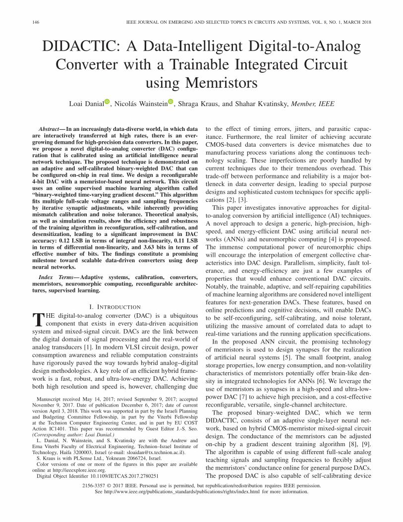
The simplest type of DAC uses a binary-weighted architec-ture [1], where N (number of bits) binary-weighted distributedelements (e.g., current sources, resistors, or capacitors) arecombined to provide a discrete analog output with finiteresolution. The binary-weighted DAC is based on a simpleand intuitive concept that utilizes the fundamental rule-of-thumb binary to decimal basis transformation. The directconversion feature can be exploited for high-speed applica-tions [1] because it uses a minimal number of conventionalcomponents and small die area. This DAC topology relies onthe working principle of the inverting summing operationalamplifier circuit, as shown in Fig. 1. Hence, the output voltageis the inverted sum of the input voltages, weighted by theratio between the feedback resistor and the series resistancefor each input. Digital inputs follow full-scale voltages, whichmeans that logical ‘1’ is equivalent to VD D, and similarly,logical ‘0’ is equivalent to 0 V. The LSB input is connectedto the highest resistance value, which equals the feedbackresistance R. Accordingly, the MSB input is connected to thelowest resistance value R/2N−1. The other bits are correspond-ingly determined in a binary-weighted fashion. The resultingdiscrete voltage of the amplifier output is
Vout = − 1
2N
N−1∑
i=0
2i Vi , (1)
where the minus sign is a result of the inverting operationalamplifier, and Vi is the digital voltage input of a bit withindex i , after it has been attenuated by 2N , which is a normal-ization factor that fits the full-scale voltage. The output voltageis proportional to the binary value of the word VN−1 . . . V0.
Despite the simplicity of the binary-weighted DAC concept,critical practical shortcomings have hindered its realization.
Fig. 1. Binary-weighted resistors based DAC.
The variability of the resistors, which defines the ratio betweenthe MSB and LSB coefficients (dynamic range), is enormousand grows exponentially with the number of resolution bits,making accurate matching very difficult, and overwhelminga huge asymmetric area with power starved resistors, e.g.,for N bits the ratio equals 2N−1. Furthermore, maintainingaccurate resistance values over a wide range is problematic.In advanced submicron CMOS fabrication technologies, it ischallenging to manufacture resistors over a wide resistancerange and preserve an accurate ratio, especially in the presenceof temperature variations. Process imperfections degrade theconversion precision and increase the vulnerability to mis-match errors, as listed in Table III in terms of INL, DNL,and ENOB.
Therefore, practical limitations, scalability drawbacks, andreal-time variations are making the analog output Vout , deter-mined by (1), non-deterministic and pushing binary-weightedDACs out of the band of interest of both high-speed andhigh-precision applications. Tremendous efforts have beeninvested in developing novel techniques using CMOS toeliminate mismatch errors; such techniques include self-calibration [10] or current steering [11]. Alternative architec-tures, e.g., fully/partially segmented DACs, have emerged toachieve better accuracy and robustness [11].
B. Memristors
The memristor was originally proposed in 1971 byChua [12] as the missing fourth fundamental passive circuitelement. Memristors are two-terminal analog passive deviceswith varying resistance, which changes according to a timeintegral of the current flowing through the device, or alter-natively, the integrated voltage across the device. Memristorsare non-volatile by definition, and in their physical realization,they are usually fabricated in the back-end-of-line (BEOL)of the CMOS process using only a few masks [13]. Therelatively small size of physical memristors enables the inte-gration of memory with computing elements, allowing com-pact, dense, and efficient parallel architecture for a varietyof applications such as memory [14], analog circuits [15],logic design [16], machine learning algorithms [17] andANNs [8]. The activation-dependent dynamics of memristorsmake them a promising feature for registering and updatingsynaptic weights. Thus, it is attractive to integrate memristors
148 IEEE JOURNAL ON EMERGING AND SELECTED TOPICS IN CIRCUITS AND SYSTEMS, VOL. 8, NO. 1, MARCH 2018
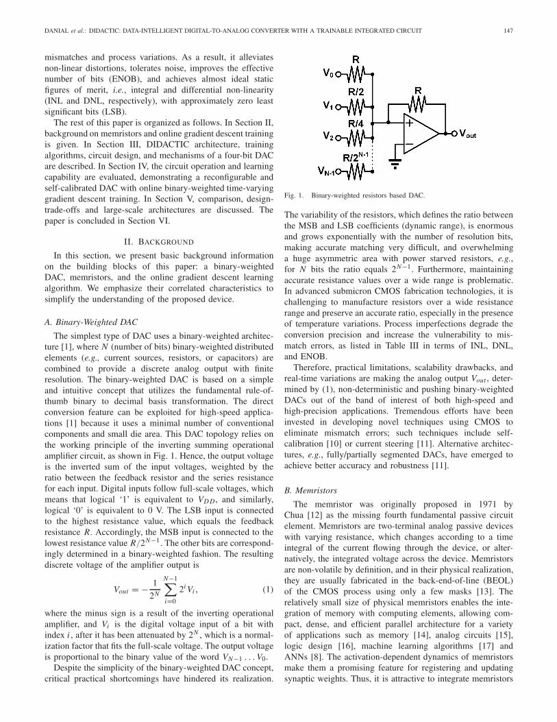
Fig. 2. Flow of the online binary-weighted time-varying gradient descent training algorithm, which updates the weights according to the error function.
as weighted elements in binary-weighted DACs [7] to achievehigh energy-efficiency and scalability. In previous work [8], weproposed the following small signal analysis model of mem-ristors, which perfectly describes the memory state derivationof synaptic weights:
i(t) = G (s(t)) v(t), (2)ds(t)
dt= f (v(t), s(t)), (3)
where s is a general state variable that evolves accordingto a function of voltage f . Eq. (2) is Ohm’s law for atime-varying conductance G. Thus, the memristor enables anefficient design of trainable neural networks in hardware [8].The VTEAM model [18] is used in this paper to accuratelymodel the non-linear memristive behaviors in our design andevaluation.
C. Online Gradient Descent Algorithm
The field of machine learning (ML) is dedicated to the studyand implementation of systems that can learn from data, andevolve their cognitive ability to make crucial decisions basedon a training phase. ANNs and neuromorphic computing arewell-established infrastructures that apply brain-inspired learn-ing rules to interpolate novel computational abilities [4], e.g.,adaptation and self-repair, beyond the conventional paradigm.In previous work [8], we analyzed a simple neural networktopology (perceptron), comprising a single layer of binaryinputs Vi , synapses W i (decimal weights), and a single neuron.The neuron is considered the de facto neuroprocessing elementthat performs the following dot product of inputs and weights,
A =N−1∑
i=0
Wi Vi , (4)
where A is an analog result of the digital inputs’ weightedsum. From this stage, both deterministic and non-deterministicequivalence between (1) and (4) are derived. Thus, the discretevoltage of the DAC output as defined in (1) can be seenas a special case of a single-layer ANN, and (4) could beadjusted, using AI learning methods, to behave as a binary-weighted DAC with intrinsic variations. To the best of our
knowledge, no neural based DAC has been developed in thepast. We exploit the neural network’s intelligent properties toachieve an adaptive DAC that is trained online by an MLalgorithm.
Assume a learning system that operates on K discrete trials,with N digital inputs V (k)
i , actual discrete output A(k) as in (4),and desired labeled output (i.e., teaching signal) t(k). Theweight W i is tuned to minimize the following mean squareerror (MSE) of the DAC through the training phase
E = 1
2
K∑
k=1
(A(k) − t(k)
)2. (5)
A reasonable iterative update rule for minimizing (5) (i.e.,updating W , where initially W is arbitrarily chosen) is thefollowing online stochastic gradient descent iteration,
�W (k)i = −η
∂ E
∂W (k)i
⇒ �W (k)i = −η
∂ E
∂ A(k)· ∂ A(k)
∂Wi
⇒ �W (k)i = −η
(A(k) − t(k)
)V (k)
i , (6)
where η is the learning rate, a small positive constant,and during each iteration k, a single empirical sample ofthe digital input voltage V (k), is chosen randomly. Thislearning algorithm, called Adaline or LMS [19], is widelyused in adaptive signal processing and control systems [20].Note that (6) is a local update rule, i.e., the change insynaptic weight Wi depends only on the related componentsA(k), t(k), and V (k)
i . This local update, which is ubiquitous inANN training and ML algorithms, enables a massively parallelacceleration. The training phase continues until the MSE isless than Ethreshold , a small predefined constant thresholdthat quantifies the learning accuracy. Due to the periodicitycharacteristic of the data used in digital-to-analog conversion,the convergence time scale is inversely proportional to thebit significance degree. For example, if the digital inputs arerandomly generated, then the expectation of their correspond-ing teaching analog label will be in the middle of the analogdynamic range. The MSB, which divides the data range intotwo different sections, will begin its adjustment proceduretowards the error gradient descent. In the same way, other
DANIAL et al.: DIDACTIC: DATA-INTELLIGENT DIGITAL-TO-ANALOG CONVERTER WITH A TRAINABLE INTEGRATED CIRCUIT 149
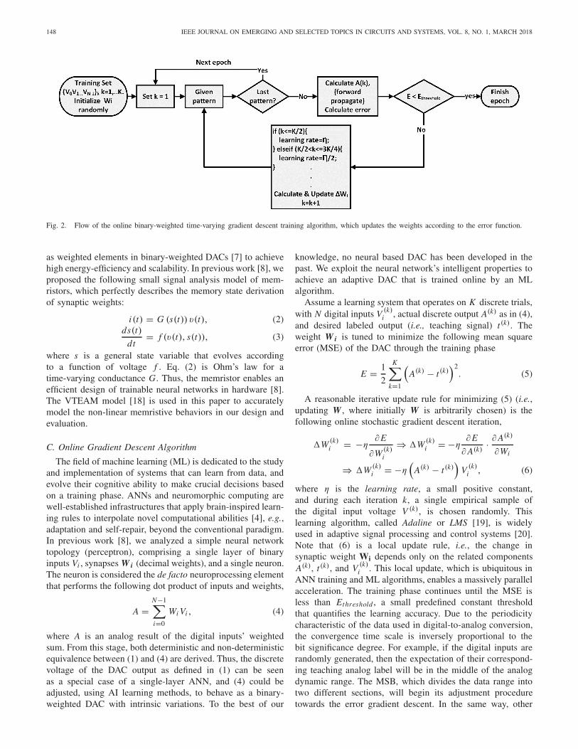
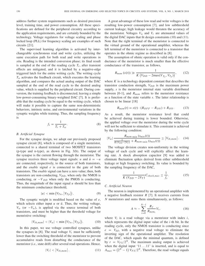
Fig. 3. (a) Schematic of a four-bit adaptive DAC based on a single layer ANN and binary-weighted synapses, trained online by a supervised learningalgorithm executed by the feedback. (b) Schematic of the memristive synapse. (c) Feedback circuit for the gradient descent learning algorithm. (d) Schematicof the PWM circuit [9] that generates fixed amplitude pulses with a time width proportional to the subtraction product between the real and teaching signals.
bits will gradually begin their adjustment procedure later, afterthey converge to their relevant sections. Therefore, the trainingdynamics of less significant bits is complex and requires moretime to be captured. Hence, the convergence time expectationis also binary-weighted distributed.
The LSB, which represents the most precise quantum,requires the longest resolution match and the lengthiest train-ing time to converge. While the MSB can quickly achievea stable value, the LSB may still present oscillations, thuscontinuously changing the collective error function in (5).Concurrently, the MSB will be disturbed and swing backand forth recursively in a deadlock around a fixed point.This problem is aggravated in the presence of noise andvariations, and ameliorated by using smaller learning rates.Hence, we propose a slightly modified update rule to guaranteea global minimum of the error, and to fine-tune the weightsproportionally to their significance degree. We call the mod-ified rule the binary-weighted time-varying gradient descentlearning rule, expressed as
�W (k)i = −η(t)
(A(k) − t(k)
)· V (k)
i , (7)
where η(t) is a time-varying learning rate, decreasing in abinary-weighted manner along with the training time, as shownin Fig. 2. The expression for η(t) is
η(t) =
⎧⎪⎪⎪⎪⎪⎪⎨
⎪⎪⎪⎪⎪⎪⎩
η i f k ≤ K/2
η/2 i f K/2 < k ≤ 3K/4
. . .
η/2N−1 i f (2N−1 − 1) · K/2N−1 < k ≤ (2N − 1)
·K/2N .
This learning rule utilizes the convergence time accelerationand the decaying learning rate to reduce bit fluctuations arounda fixed point. In Section IV, we show that this learning ruleis better than (6) in terms of training time duration, accuracy,and robustness to learning rate non-uniformity.
III. NEURAL NETWORK DAC ARCHITECTURE
In this section, we present DIDACTIC, our proposed DACarchitecture. We begin with a system overview, followed by thecircuit design. Finally, the learning algorithm implementationis presented.
A. System Overview
We leverage the conceptual simplicity, parallelism level, andminimum die size of the binary-weighted DAC architectureby implementing online gradient descent in hardware, thusachieving a reconfigurable, accurate, adaptive, and scalableDAC that can be used for high-speed, high-precision, and cost-effective applications. In Fig. 3(a), the proposed architecturefor a four-bit neural network DAC is shown. As mentioned,the device is based on memristive synapses that collectivelyintegrate through the operational amplifier, and a feedbackcircuit that regulates the value of the weights in real timeaccording to (7). The architecture is composed of four synapseunits, one neuron unit, and a synchronous training unit.
Depending on the characteristics and requirements of theapplication, a set of system parameters is determined. First,the sampling frequency fs , which specifies the DAC speed,is determined, followed by the number of resolution bits N ,which specifies the accuracy of the converter, and then thefull-scale voltage VF S , which specifies the DAC input dynamicrange. Dynamic specifications concerning the learning rate aretaken into consideration during the training phase, in order to
150 IEEE JOURNAL ON EMERGING AND SELECTED TOPICS IN CIRCUITS AND SYSTEMS, VOL. 8, NO. 1, MARCH 2018
address further system requirements such as desired precisionlevel, training time, and power consumption. All these speci-fications are defined for the peripheral circuitry according tothe application requirements, and are certainly bounded by thetechnology. Voltage regulators for voltage scaling and phaselocked loop (PLL) for frequency scaling are examples of suchcircuits [21].
The supervised learning algorithm is activated by inter-changeable synchronous read and write cycles, utilizing thesame execution path for both read and write operations insitu. Reading is the intended conversion phase; its final resultis sampled at the end of the reading cycle Tr , after transienteffects are mitigated, and it is latched by a negative-edgetriggered latch for the entire writing cycle. The writing cycleTw activates the feedback circuit, which executes the learningalgorithm, and compares the actual analog output of the DACsampled at the end of the read cycle to the desired analogvalue, which is supplied by the peripheral circuit. During con-version, the training feedback is disconnected, leaving a simplelow-power-consuming binary-weighted DAC [7]. It is prefer-able that the reading cycle be equal to the writing cycle, whichwill make it possible to capture the same non-deterministicbehaviors, intrinsic noise, and environmental variations in thesynaptic weights while training. Thus, the sampling frequencyis
fs = 1
Tr + Tw. (8)
B. Artificial Synapse
For the synapse design, we adopt our previously proposedsynapse circuit [8], which is composed of a single memristor,connected to a shared terminal of two MOSFET transistors(p-type and n-type), as shown in Fig. 3(b). The output ofthe synapse is the current flowing through the memristor. Thesynapse receives three voltage input signals: u and u = −uare connected, respectively, to the source of both transistors,and the enable signal e is connected to the gate of bothtransistors. The enable signal can have a zero value; then, bothtransistors are non-conducting, VD D, when only the NMOS isconducting, or −V D D when only the PMOS is conducting.Thus, the magnitude of the input signal u should be less thanthe minimum conductance threshold,
|u| < min(VT n,
∣∣VT p∣∣) . (9)
The synaptic weight is modified based on the value of e,which selects either input u or u. Thus, the writing voltage,Vw (or −Vw), is applied via the source terminal of bothtransistors, and must be higher than the threshold voltage formemristive switching:
|Vth,mem | < |Vw| < min(VT n,
∣∣VT p∣∣). (10)
In this paper, we use voltage controlled synapses, unlikethe synapses in [8]. The read voltage Vr must be sufficientlylower than the switching threshold of the memristor to preventaccumulative reads from disturbing the conductance of thememristor (i.e., state drift) after several read operations. Hence,
|Vr | <∣∣Vth,mem
∣∣ . (11)
A great advantage of these low read and write voltages is theresulting low-power consumption [7], and low subthresholdcurrent leakage; high leakage would threaten the accuracy ofthe memristor. Voltages Vw and Vr are attenuated values ofthe digital DAC inputs that fit design constraints (10) and (11).Note that the right terminal of the memristor is connected tothe virtual ground of the operational amplifier, whereas theleft terminal of the memristor is connected to a transistor thatoperates in the ohmic regime as described in [8].
The assumption of ohmic operation is valid only if the con-ductance of the memristor is much smaller than the effectiveconductance of the transistor, as follows,
Rmem (s(t)) � 1
K(VD D − 2max(V Tn , VTp)
) , (12)
where K is a technology dependent constant that describes thetransistor conduction strength, VD D is the maximum powersupply, s is the memristor internal state variable distributedbetween [0-1], and Rmem refers to the memristor resistanceas a function of the state variable s. The latter relationship ischosen to be linear [18]
Rmem(t) = s(t) · (RO F F − RO N ) + RO N . (13)
As a result, the memristor resistance level that couldbe achieved during training is lower bounded. Otherwise,the applied voltage over the memristor during the write cyclewill not be sufficient to stimulate it. This constraint is achievedby the following condition:
|Vw| Rmem ,min (smin(t))1
K (VDD−2VT ) + Rmem ,min (smin(t))≥ ∣∣Vth,mem
∣∣ . (14)
The voltage division creates non-uniformity in the writingvoltage of each cycle and will explicitly affect the learn-ing rate. A shock absorption capacitor [9] was added toeliminate fluctuation spikes derived from either subthresholdleakage or high frequency switching. Its value is bounded bythe sampling frequency of the DAC,
1
K (VD D − 2VT )Cshock,max ≤ 1
fs. (15)
C. Artificial Neuron
The neuron is implemented by an operational amplifier witha negative feedback resistor R [7]. It receives currents fromN memristors and sums them simultaneously, as follows:
A ≈ −N−1∑
i=0
R f
Rmemi
Vi , (16)
where Vi is a read voltage via a memristor with index i ,which represents the digital input value of the i -th bit. In thereading cycle, only the NMOS transistor is conducting sincee = Vdd , with a negative read voltage to eliminate theinverting sign of the operational amplifier. The resolutionof the DAC, which equals the minimal quantum, is definedby r = VF S/2N . The maximum analog output is achievedwhen the digital input ‘11 . . .11’ is inserted, and is equal toAmax = (
2N − 1)
VF S/2N . Therefore, the read voltage equals
DANIAL et al.: DIDACTIC: DATA-INTELLIGENT DIGITAL-TO-ANALOG CONVERTER WITH A TRAINABLE INTEGRATED CIRCUIT 151
TABLE I
CIRCUIT PARAMETERS
Vr = r = VF S/2N , and it should obey the constraints in (11).Based on this read voltage, bounds on the number of resolutionbits that the DAC could hold were formalized. From (11),we extract the minimal number of resolution bits,
Nmin ≥⌈
log2
(VF S
min(VTn , VTp
))⌉
, (17)
where the maximal number of resolution bits is boundedby the binary-weighted levels within the dynamic range ofthe memristor, Nmax ≤ log2
(ROF FRON
). Because of the serial
transistor resistance, however, it is undesirable to use sur-rounding levels. Doing so decreases the number of bits bylog2
⌈1
RON K (VDD−2VT )
⌉, which is approximated to be zero in
our case because RO N � 1/K (VD D − 2VT ). Additionally,in the case of smaller full-scale voltage, some levels shouldbe reserved. For example, if the full-scale voltage is half ofthe maximum power supply VF S = V D D/2, then the high-est binary-weighted level should be reserved. Doing so willdecrease the effective number of bits by
⌈log2
(VDD
VFs,min
)⌉. The
maximum number of bits that the proposed DAC could convertis up to
Nmax ≤ log2
(RO F F
RO N
)− log2
⌈1
RON K (VD D − 2VT )
⌉
−⌈
log2
(VD D
VFs,min
)⌉. (18)
In this case, if the minimal full-scale voltage is VF S = V D D/2,then the number of bits that could be converted by a DAC withthe device parameters listed in Table I is at most four.
In the same context, the feedback resistor is upper-boundedby the minimal full-scale voltage and the highest resistance ofthe memristor,
R f ≤ RO F F VF S
VD D, (19)
when considering bi-directional variations of the trainingabove and below the fixed resistance level, respectively. Thesevariations are evaluated as ±10% of the nominal value.
D. Feedback Training Unit
The feedback circuit is the main component for the exe-cution of the binary-weighted time-varying gradient descentalgorithm, which precisely regulates the synaptic adaptationprocedure. Our aim is to design (7) in hardware and implementbasic subtraction and multiplication operations. The subtrac-tion discrete voltage product (namely, the error) is pulsemodulated by a pulse-width modulator (PWM) with timewidth linearly proportional to the error and ±VD D, 0 V pulselevels. As illustrated in Fig. 3(c), the PWM product is applied,via the feedback loop, to the synapse as an enable signal.The PWM [9], as shown in Fig. 3(d), is controlled by aclock that determines the maximum width of the productpulse. If sign (A − T ) ≥ 0, then the NMOS is conductingand the subtraction amplitude is compared to a positive rampwith full-scale voltage and clock cycle time width. Otherwise,the PMOS is conducting and the subtraction amplitude iscompared to a negative ramp with full-scale voltage and clockcycle time width. As implied in (7), the learning rate is timevarying. This is achieved by controlling the PWM with clockswith binary-weighted frequency multiples.
Therefore, the multiplication is invoked as an AND logicgate and controlled by the modulated enable signal, whereasthe attenuated digital input is connected via the source of thesynapse. The input is attenuated to obey the constraint in (10),as specified in Table I. The learning rate is a key factor of theadaptation performance: it depends on the circuit parameterslisted in Table I, and on the write voltage, pulse-time width,feedback resistor, present state, and memristor device physicalproperties. The learning rate is
η(t) = �R
R= (RO F F − RO N )�s(t)
R f, (20)
152 IEEE JOURNAL ON EMERGING AND SELECTED TOPICS IN CIRCUITS AND SYSTEMS, VOL. 8, NO. 1, MARCH 2018
where �s is the change in the memristor internal state, and isdefined as in the VTEAM model,
�s =Tw∫
0
Kon/of f
(VW
Von/of f− 1
)αon/o f f
· f (s)dt, (21)
where Kon/of f , and αon/of f are constants that describe thestate evolution rate and its nonlinearity, respectively, Von/of f
are voltage thresholds, and f (s) is a window function thatadds nonlinearity and state dependency during state evolution.These parameters are fitted to the Pt/HfOx/Hf/TiN RRAMdevice with a buffer layer [22], with a high-to-low resistancestate ratio of ∼50 and low forming, set and reset voltages.
IV. EVALUATION
In this section, the proposed four-bit DAC design is dis-cussed and evaluated in a SPICE simulation using a 0.18μ mCMOS process and the VTEAM memristor model [18]. First,the learning algorithm is evaluated in terms of mean squareerror (MSE) and training time. Then, a static evaluation ofthe circuit is described, and finally the dynamic evaluationis presented. The proposed DAC has been tested in bothideal and non-ideal cases. The circuit parameters, architecturalspecifications, and design constraints are listed in Table I.
A. Ideal Case
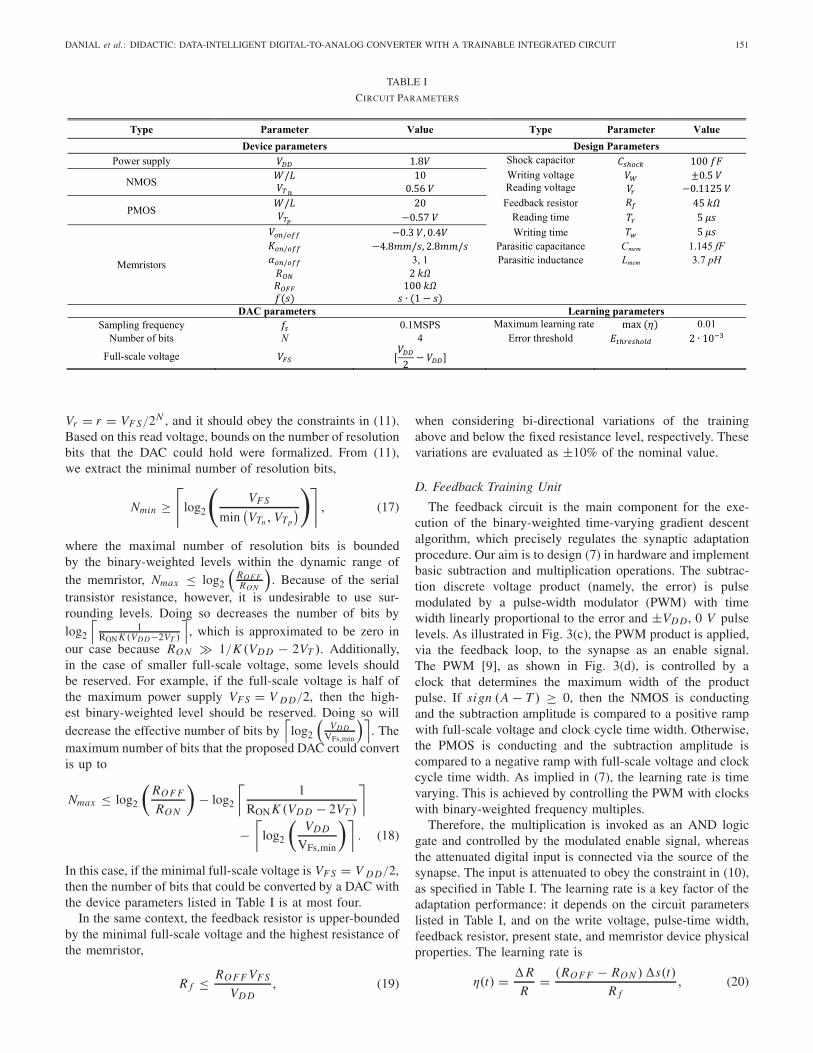
The basic deterministic functionality of the four-bit DACis demonstrated while being trained by the online gradientdescent algorithm. Figure 4(a) shows the synapse resistivevalue where two sawtooth training datasets with differentfull-scale voltage ranges (VD D, and VD D/2) are applied suc-cessively in real time. It can be observed that the networkconverges from a random initial state to a steady state oncethe error determined by (5) is lower than Ethreshold , after∼2000 training samples. Furthermore, it can be observed thatwhen the full-scale voltage changes to VD D/2, the systemconverges to a new steady state that quantizes 0.9V full-scale. In each case, the network is successfully reconfiguredto operate under different specifications, as shown by differentbinary-weighted synaptic values in Fig. 4(a).
The DAC is next evaluated in terms of accuracy and trainingtime, as illustrated in Fig. 4(b–d). The static evaluation inresponse to the DC ramp signal at three different time stampsis shown in Fig. 4(b) for (I) the initial state before training,(II) coarse-grained training (i.e., where the error is slightlyhigher than Ethreshold), and (III) fine-grained training (i.e.,where the error is low enough and the DAC response convergesto the final, desired state). The teaching staircase in Fig. 4(b)is the same DC ramp input that statically evaluates the DACat the three given time stamps. Therefore, the differencesbetween two adjacent digital input codes within the actualDAC output are the differential non-linearity (DNL), andsimilarly, the total voltage differences between the actual DACoutput and the desired staircase for each digital input code arethe integral non-linearity (INL). Results of the DNL and INLare shown, respectively, in Fig. 4(c) and 4(d).
Fig. 4. (a) Binary-weighted synaptic adaptation during the training phasefor the 1.8V full-scale output voltage range. Immediately, synapses aretrained for the 0.9V full-scale output voltage range and shown in real time.(b) Comparison between the teaching dataset and the actual neural discreteanalog DAC output at three different time stamps during the training; anidentical staircase is achieved after the training is complete. (c) Differentialand (d) integral non-linearities of the DAC at three different time stamps inresponse to the DC input voltage ramp.
As shown in Fig. 4(c–d), before the training state the DAC iscompletely non-linear and non-monotonic, with several miss-ing codes. Thus, the maximum difference between the discrete
DANIAL et al.: DIDACTIC: DATA-INTELLIGENT DIGITAL-TO-ANALOG CONVERTER WITH A TRAINABLE INTEGRATED CIRCUIT 153
analog output and the ideal staircase, and the maximum dif-ference between two adjacent analog levels, are considerablyhigh: INL ≈ −32 LSB, and DNL ≈ −13 LSB. At the secondtime stamp (2ms ∼ 200 samples), however, the DAC performsbetter and appears monotonic but not sufficiently accurate(INL ≈ −1 LSB, DNL ≈ −1 LSB). After the training iscomplete (20ms), the DAC is fully calibrated: INL ≈ 0 LSB,and DNL ≈ 0 LSB. The fact that the DNL and INL are almostideal proves that the training algorithm achieves maximumperformance. The DAC also showed robustness when it wassimulated with a randomly generated training dataset.
The improvements in static figures of merit significantlyaffect the dynamic figures of merit. The ENOB is a functionof signal-to-noise and distortion ratio, whereas the distortionsare a result of the DAC’s non-linearity. If the DAC is non-linear (e.g., INL, DNL �=0), then harmonic distortion spurs willappear in the dynamic response, degrading the ENOB [1].Therefore, improving the INL and DNL by learning andcalibration techniques alleviates distortions and improves theENOB, improving the precision of the DAC. To evaluate theENOB, the DAC is dynamically evaluated and analyzed inresponse to a sine input with 40 k H z frequency, which meetsthe Nyquist condition: finput ≤ fs/2. The achieved ENOBin the ideal case is 3.71, which is almost ideal consideringthe intrinsic quantization error. All the extracted performancemetrics are summarized in Table III.
B. Non-Ideal Case
Usually, analog domains suffer from reduced robustnessand vulnerability to noise and variations in comparison totheir digital counterparts. DACs are being continuously pushedtowards their performance limits as technology scales downand system specifications become more challenging. Whiledevice mismatch and process imperfections in modern DACscan be compensated for by calibration mechanisms [10], noisecan irreparably degrade performance and is less straightfor-ward to capture at design time. Several analysis methodshave been established to estimate noise sources and theirimpact on the performance [23], [24]. All these mechanismsare specific and technology dependent, requiring exhaustivecharacterization, massive validation, and relatively long devel-opment time-to-market. Adaptive intelligent systems motivatedby machine learning algorithms are, however, inherently robustto noise, which is a key element in the set of problemsthey are designed to solve. This suggests that the effectsof intrinsic noise on the performance of the analog circuitare relatively small. Therefore, online training algorithms arenot exclusive to reconfiguration, but can also be used forself-calibration, adaptation, and noise tolerance with genericstandard methodology [8].
For this reason, a crude estimation of the magnitude ofnoise and variability has been extracted from [8], [23]–[30]and characterized as listed in Table II:
1. The process variation parameters for the memristor arepessimistically chosen, with a coefficient of variation(CV = standard deviation/mean ∼10%) to cover widereliability margins [8]. The variability in the parameters
TABLE II
CIRCUIT VARIATIONS & NOISE
of the memristors is equivalent either to correspondingchanges in the synaptic weights or to the learning rateη. In Fig. 5, we show that the proposed binary-weightedtime-varying gradient descent training algorithm is ableto tolerate such process variations over time. The vari-ability in the transistor parameters can also dramaticallyaffect the learning performance; thus, transistor parame-ters such as VW , W/L, and VT in Table I are chosen toguarantee a global optimal solution even in such extremescenarios.
2. Noise sources include intrinsic thermal noise comingfrom the feedback resistor, memristor, and transistor [8],as well as pulse-width modulation noise, input referrednoise [23], training label fluctuations as a result of sup-plier converter quantization noise [27], and frequency-dependent noise sources, which are quantified andestimated [28].
3. Frequency-dependent variations capture the parasiticcapacitance and inductance of the memristor [29] andmodel it by a varying impedance as a function ofthe frequency. In addition, �R degradation [30] alongswitching cycles as a result of oxide defects and deviceaging is considered.
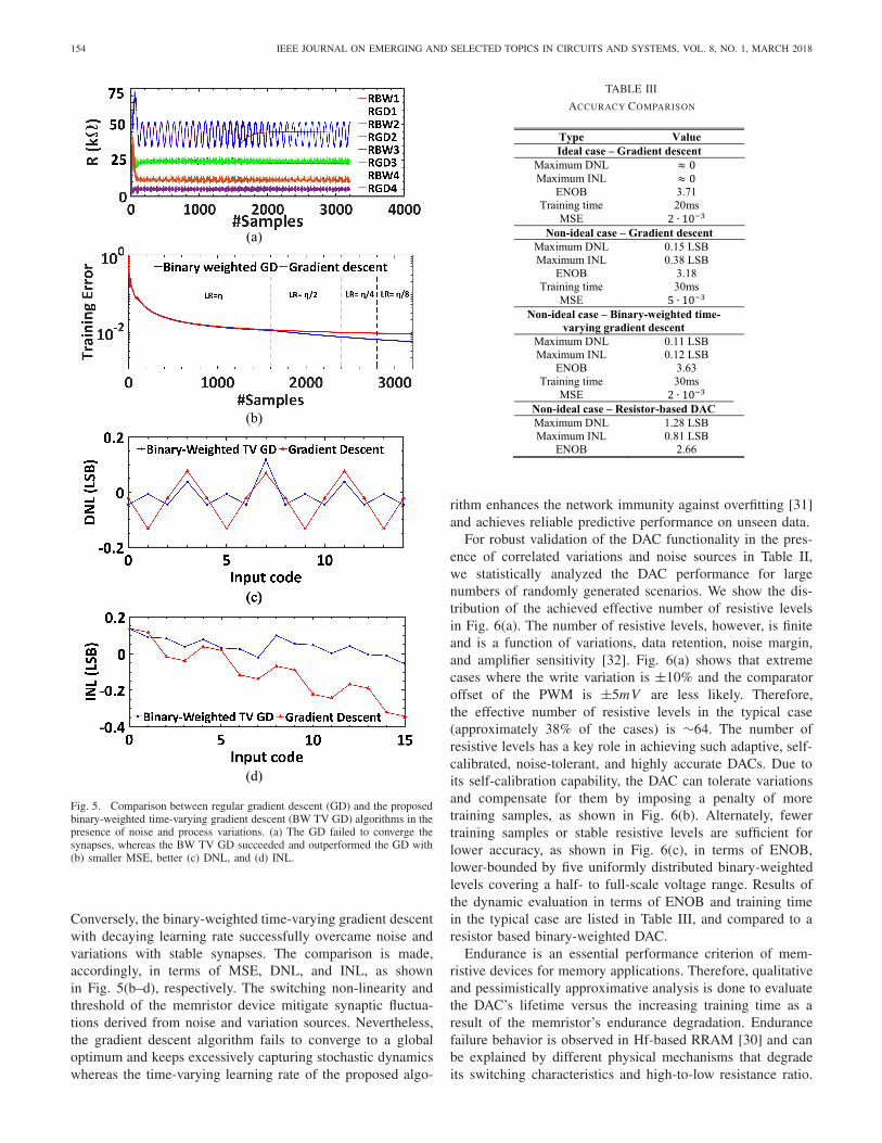
While process variations determine the convergence timeand accuracy, noise can cause the network to deviate from theoptimum weights with destructive oscillations. In Fig. 5(a),the training processes for both gradient descent and thebinary-weighted time-varying gradient descent with decayinglearning rate are shown. Observe that the regular gradientdescent, which succeeded in stabilizing the synapses withoutthe presence of noise, now fails to stabilize the synapses.
154 IEEE JOURNAL ON EMERGING AND SELECTED TOPICS IN CIRCUITS AND SYSTEMS, VOL. 8, NO. 1, MARCH 2018
Fig. 5. Comparison between regular gradient descent (GD) and the proposedbinary-weighted time-varying gradient descent (BW TV GD) algorithms in thepresence of noise and process variations. (a) The GD failed to converge thesynapses, whereas the BW TV GD succeeded and outperformed the GD with(b) smaller MSE, better (c) DNL, and (d) INL.
Conversely, the binary-weighted time-varying gradient descentwith decaying learning rate successfully overcame noise andvariations with stable synapses. The comparison is made,accordingly, in terms of MSE, DNL, and INL, as shownin Fig. 5(b–d), respectively. The switching non-linearity andthreshold of the memristor device mitigate synaptic fluctua-tions derived from noise and variation sources. Nevertheless,the gradient descent algorithm fails to converge to a globaloptimum and keeps excessively capturing stochastic dynamicswhereas the time-varying learning rate of the proposed algo-
TABLE III
ACCURACY COMPARISON
rithm enhances the network immunity against overfitting [31]and achieves reliable predictive performance on unseen data.
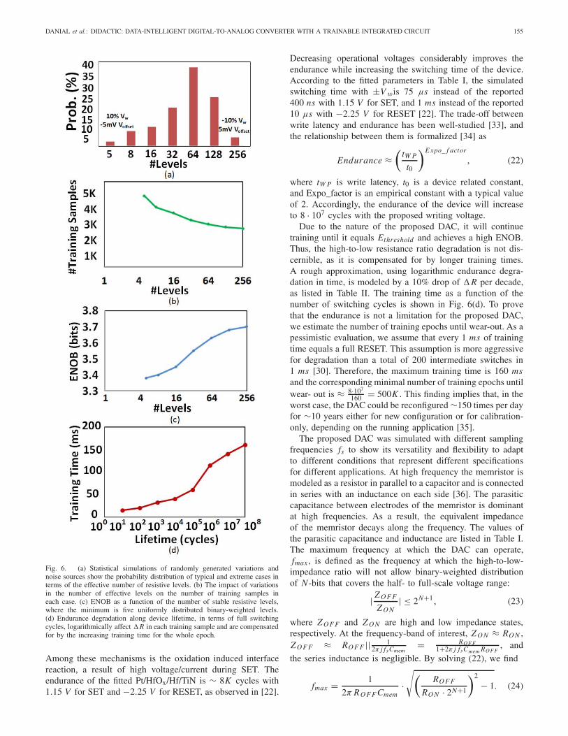
For robust validation of the DAC functionality in the pres-ence of correlated variations and noise sources in Table II,we statistically analyzed the DAC performance for largenumbers of randomly generated scenarios. We show the dis-tribution of the achieved effective number of resistive levelsin Fig. 6(a). The number of resistive levels, however, is finiteand is a function of variations, data retention, noise margin,and amplifier sensitivity [32]. Fig. 6(a) shows that extremecases where the write variation is ±10% and the comparatoroffset of the PWM is ±5mV are less likely. Therefore,the effective number of resistive levels in the typical case(approximately 38% of the cases) is ∼64. The number ofresistive levels has a key role in achieving such adaptive, self-calibrated, noise-tolerant, and highly accurate DACs. Due toits self-calibration capability, the DAC can tolerate variationsand compensate for them by imposing a penalty of moretraining samples, as shown in Fig. 6(b). Alternately, fewertraining samples or stable resistive levels are sufficient forlower accuracy, as shown in Fig. 6(c), in terms of ENOB,lower-bounded by five uniformly distributed binary-weightedlevels covering a half- to full-scale voltage range. Results ofthe dynamic evaluation in terms of ENOB and training timein the typical case are listed in Table III, and compared to aresistor based binary-weighted DAC.
Endurance is an essential performance criterion of mem-ristive devices for memory applications. Therefore, qualitativeand pessimistically approximative analysis is done to evaluatethe DAC’s lifetime versus the increasing training time as aresult of the memristor’s endurance degradation. Endurancefailure behavior is observed in Hf-based RRAM [30] and canbe explained by different physical mechanisms that degradeits switching characteristics and high-to-low resistance ratio.
DANIAL et al.: DIDACTIC: DATA-INTELLIGENT DIGITAL-TO-ANALOG CONVERTER WITH A TRAINABLE INTEGRATED CIRCUIT 155
Fig. 6. (a) Statistical simulations of randomly generated variations andnoise sources show the probability distribution of typical and extreme cases interms of the effective number of resistive levels. (b) The impact of variationsin the number of effective levels on the number of training samples ineach case. (c) ENOB as a function of the number of stable resistive levels,where the minimum is five uniformly distributed binary-weighted levels.(d) Endurance degradation along device lifetime, in terms of full switchingcycles, logarithmically affect �R in each training sample and are compensatedfor by the increasing training time for the whole epoch.
Among these mechanisms is the oxidation induced interfacereaction, a result of high voltage/current during SET. Theendurance of the fitted Pt/HfOx/Hf/TiN is ∼ 8K cycles with1.15 V for SET and −2.25 V for RESET, as observed in [22].
Decreasing operational voltages considerably improves theendurance while increasing the switching time of the device.According to the fitted parameters in Table I, the simulatedswitching time with ±V wis 75 μs instead of the reported400 ns with 1.15 V for SET, and 1 ms instead of the reported10 μs with −2.25 V for RESET [22]. The trade-off betweenwrite latency and endurance has been well-studied [33], andthe relationship between them is formalized [34] as
Endurance ≈(
tW P
t0
)Expo_ f actor
, (22)
where tW P is write latency, t0 is a device related constant,and Expo_factor is an empirical constant with a typical valueof 2. Accordingly, the endurance of the device will increaseto 8 · 107 cycles with the proposed writing voltage.
Due to the nature of the proposed DAC, it will continuetraining until it equals Ethreshold and achieves a high ENOB.Thus, the high-to-low resistance ratio degradation is not dis-cernible, as it is compensated for by longer training times.A rough approximation, using logarithmic endurance degra-dation in time, is modeled by a 10% drop of �R per decade,as listed in Table II. The training time as a function of thenumber of switching cycles is shown in Fig. 6(d). To provethat the endurance is not a limitation for the proposed DAC,we estimate the number of training epochs until wear-out. As apessimistic evaluation, we assume that every 1 ms of trainingtime equals a full RESET. This assumption is more aggressivefor degradation than a total of 200 intermediate switches in1 ms [30]. Therefore, the maximum training time is 160 msand the corresponding minimal number of training epochs untilwear- out is ≈ 8·107
160 = 500K . This finding implies that, in theworst case, the DAC could be reconfigured ∼150 times per dayfor ∼10 years either for new configuration or for calibration-only, depending on the running application [35].
The proposed DAC was simulated with different samplingfrequencies fs to show its versatility and flexibility to adaptto different conditions that represent different specificationsfor different applications. At high frequency the memristor ismodeled as a resistor in parallel to a capacitor and is connectedin series with an inductance on each side [36]. The parasiticcapacitance between electrodes of the memristor is dominantat high frequencies. As a result, the equivalent impedanceof the memristor decays along the frequency. The values ofthe parasitic capacitance and inductance are listed in Table I.The maximum frequency at which the DAC can operate,fmax , is defined as the frequency at which the high-to-low-impedance ratio will not allow binary-weighted distributionof N-bits that covers the half- to full-scale voltage range:
| Z O F F
Z O N| ≤ 2N+1, (23)
where Z O F F and Z O N are high and low impedance states,respectively. At the frequency-band of interest, Z O N ≈ RO N ,Z O F F ≈ RO F F || 1
2π j fsCmem= ROF F
1+2π j fsCmem ROF F, and
the series inductance is negligible. By solving (22), we find
fmax = 1
2π RO F F Cmem·√(
RO F F
RO N · 2N+1
)2
− 1. (24)
156 IEEE JOURNAL ON EMERGING AND SELECTED TOPICS IN CIRCUITS AND SYSTEMS, VOL. 8, NO. 1, MARCH 2018
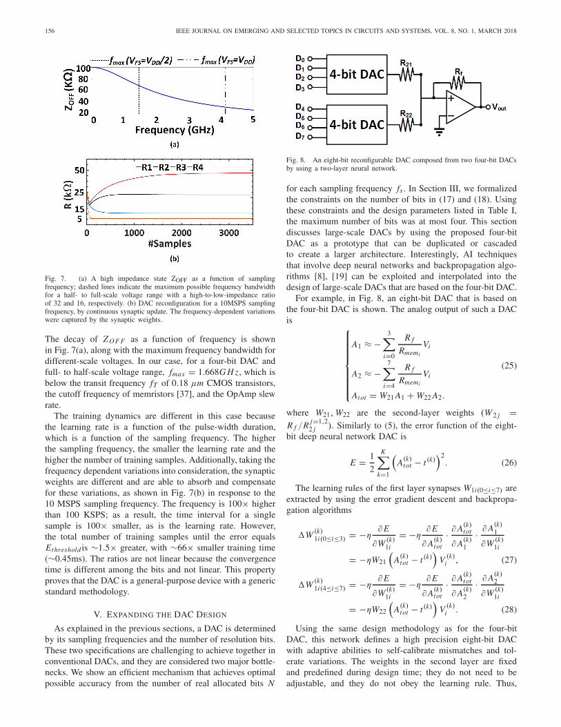
Fig. 7. (a) A high impedance state ZOFF as a function of samplingfrequency; dashed lines indicate the maximum possible frequency bandwidthfor a half- to full-scale voltage range with a high-to-low-impedance ratioof 32 and 16, respectively. (b) DAC reconfiguration for a 10MSPS samplingfrequency, by continuous synaptic update. The frequency-dependent variationswere captured by the synaptic weights.
The decay of Z O F F as a function of frequency is shownin Fig. 7(a), along with the maximum frequency bandwidth fordifferent-scale voltages. In our case, for a four-bit DAC andfull- to half-scale voltage range, fmax = 1.668G H z, which isbelow the transit frequency fT of 0.18 μm CMOS transistors,the cutoff frequency of memristors [37], and the OpAmp slewrate.
The training dynamics are different in this case becausethe learning rate is a function of the pulse-width duration,which is a function of the sampling frequency. The higherthe sampling frequency, the smaller the learning rate and thehigher the number of training samples. Additionally, taking thefrequency dependent variations into consideration, the synapticweights are different and are able to absorb and compensatefor these variations, as shown in Fig. 7(b) in response to the10 MSPS sampling frequency. The frequency is 100× higherthan 100 KSPS; as a result, the time interval for a singlesample is 100× smaller, as is the learning rate. However,the total number of training samples until the error equalsEthreshold is ∼1.5× greater, with ∼66× smaller training time(∼0.45ms). The ratios are not linear because the convergencetime is different among the bits and not linear. This propertyproves that the DAC is a general-purpose device with a genericstandard methodology.
V. EXPANDING THE DAC DESIGN
As explained in the previous sections, a DAC is determinedby its sampling frequencies and the number of resolution bits.These two specifications are challenging to achieve together inconventional DACs, and they are considered two major bottle-necks. We show an efficient mechanism that achieves optimalpossible accuracy from the number of real allocated bits N
Fig. 8. An eight-bit reconfigurable DAC composed from two four-bit DACsby using a two-layer neural network.
for each sampling frequency fs . In Section III, we formalizedthe constraints on the number of bits in (17) and (18). Usingthese constraints and the design parameters listed in Table I,the maximum number of bits was at most four. This sectiondiscusses large-scale DACs by using the proposed four-bitDAC as a prototype that can be duplicated or cascadedto create a larger architecture. Interestingly, AI techniquesthat involve deep neural networks and backpropagation algo-rithms [8], [19] can be exploited and interpolated into thedesign of large-scale DACs that are based on the four-bit DAC.
For example, in Fig. 8, an eight-bit DAC that is based onthe four-bit DAC is shown. The analog output of such a DACis
⎧⎪⎪⎪⎪⎪⎪⎪⎨
⎪⎪⎪⎪⎪⎪⎪⎩
A1 ≈ −3∑
i=0
R f
Rmemi
Vi
A2 ≈ −7∑
i=4
R f
Rmemi
Vi
Atot = W21 A1 + W22 A2.
(25)
where W21, W22 are the second-layer weights (W 2 j =R f /R j=1,2
2 j ). Similarly to (5), the error function of the eight-bit deep neural network DAC is
E = 1
2
K∑
k=1
(A(k)
tot − t(k))2
. (26)
The learning rules of the first layer synapses W1i(0≤i≤7) areextracted by using the error gradient descent and backpropa-gation algorithms
�W (k)1i(0≤i≤3) = −η
∂ E
∂W (k)1i
= −η∂ E
∂ A(k)tot
· ∂ A(k)tot
∂ A(k)1
· ∂ A(k)1
∂W (k)1i
= −ηW21
(A(k)
tot − t(k))
V (k)i , (27)
�W (k)1i(4≤i≤7) = −η
∂ E
∂W (k)1i
= −η∂ E
∂ A(k)tot
· ∂ A(k)tot
∂ A(k)2
· ∂ A(k)2
∂W (k)1i
= −ηW22
(A(k)
tot − t(k))
V (k)i . (28)
Using the same design methodology as for the four-bitDAC, this network defines a high precision eight-bit DACwith adaptive abilities to self-calibrate mismatches and tol-erate variations. The weights in the second layer are fixedand predefined during design time; they do not need to beadjustable, and they do not obey the learning rule. Thus,
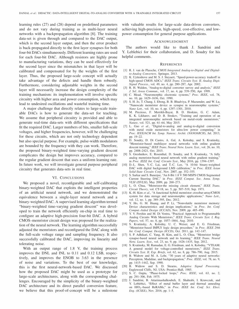
DANIAL et al.: DIDACTIC: DATA-INTELLIGENT DIGITAL-TO-ANALOG CONVERTER WITH A TRAINABLE INTEGRATED CIRCUIT 157
learning rules (27) and (28) depend on predefined parametersand do not vary during training as in multi-layer neuralnetworks with a backpropagation algorithm [8]. The trainingdata-set is given through and compared to the DAC output,which is the second layer output, and then the error productis back-propagated directly to the first layer synapses for bothfour-bit DACs simultaneously. Different learning rates are usedfor each four-bit DAC. Although resistors are highly proneto manufacturing variations, they can be used effectively forthe second layer since the mismatches in that layer will becalibrated and compensated for by the weights of the firstlayer. Thus, the proposed large-scale concept will actuallytake advantage of the defects and handle them robustly.Furthermore, considering adjustable weights in the secondlayer will necessarily increase the design complexity of thetraining mechanism: its implementation will involve specificcircuitry with higher area and power consumption, which maylead to undesired oscillations and wasteful training time.
A major challenge that directly relates to large-scale train-able DACs is how to generate the data-set for teaching.We assume that peripheral circuitry is provided and able togenerate real-time data-sets with different specifications thatfit the required DAC. Larger numbers of bits, smaller full-scalevoltages, and higher frequencies, however, will be challengingfor these circuits, which are not only technology dependentbut also special purpose. For example, pulse-width modulatorsare bounded by the frequency with they can work. Therefore,the proposed binary-weighted time-varying gradient descentcomplicates the design but improves accuracy, compared tothe regular gradient descent that uses a uniform learning rate.In future work, we will investigate general purpose peripheralcircuitry that generates data-sets in real time.
VI. CONCLUSIONS
We proposed a novel, reconfigurable and self-calibratingbinary-weighted DAC that exploits the intelligent propertiesof an artificial neural network, and we demonstrated theequivalence between a single-layer neural network and abinary-weighted DAC. A supervised learning algorithm termed“binary-weighted time-varying gradient descent” was devel-oped to train the network efficiently on-chip in real time toconfigure an adaptive high-precision four-bit DAC. A hybridCMOS–memristor circuit design was proposed for the realiza-tion of the neural network. The learning algorithm successfullyadjusted the memristors and reconfigured the DAC along withthe full-scale voltage range and sampling frequency. It alsosuccessfully calibrated the DAC, improving its linearity andtolerating noise.
With an output range of 1.8 V, the training processimproves the DNL and INL to 0.11 and 0.12 LSB, respec-tively, and improves the ENOB to 3.63 in the presenceof noise and variations. To the best of our knowledge,this is the first neural-network-based DAC. We discussedhow the proposed DAC might be used as a prototype forlarge-scale architectures, along with the corresponding chal-lenges. Encouraged by the simplicity of the binary-weightedDAC architecture and its direct parallel conversion feature,we believe that this proof-of-concept will be a milestone
with valuable results for large-scale data-driven converters,achieving high-precision, high-speed, cost-effective, and low-power consumption for general purpose applications.
ACKNOWLEDGMENT
The authors would like to thank J. Sandrini andY. Leblebici for their collaboration, and D. Soudry for hishelpful comments.
REFERENCES
[1] R. J. van de Plassche, CMOS Integrated Analog-to-Digital and Digital-to-Analog Converters. Springer, 2013.
[2] K. Uyttenhove and M. S. J. Steyaert, “Speed-power-accuracy tradeoff inhigh-speed CMOS ADCs,” IEEE Trans. Circuits Syst. II, Analog Digit.Signal Process., vol. 49, no. 4, pp. 280–287, Apr. 2002.
[3] R. H. Walden, “Analog-to-digital converter survey and analysis,” IEEEJ. Sel. Areas Commun., vol. 17, no. 4, pp. 539–550, Apr. 1999.
[4] C. Mead, “Neuromorphic electronic systems,” Proc. IEEE, vol. 78,no. 10, pp. 1629–1636, Oct. 1990.
[5] S. H. Jo, T. Chang, I. Ebong, B. B. Bhadviya, P. Mazumder, and W. Lu,“Nanoscale memristor device as synapse in neuromorphic systems,”Nano Lett., vol. 10, no. 4, pp. 1297–1301, 2010.
[6] M. Prezioso, F. Merrikh-Bayat, B. D. Hoskins, G. C. Adam,K. K. Likharev, and D. B. Strukov, “Training and operation of anintegrated neuromorphic network based on metal-oxide memristors,”Nature, vol. 521, pp. 61–64, May 2015.
[7] L. Gao et al., “Digital-to-analog and analog-to-digital conversionwith metal oxide memristors for ultra-low power computing,” inProc. IEEE/ACM Int. Symp. Nanosc. Archit. (NANOARCH), Jul. 2013,pp. 19–22.
[8] D. Soudry, D. Di Castro, A. Gal, A. Kolodny, and S. Kvatinsky,“Memristor-based multilayer neural networks with online gradientdescent training,” IEEE Trans. Neural Netw. Learn. Syst., vol. 26, no. 10,pp. 2408–2421, Oct. 2015.
[9] S. Greshnikov, E. Rosenthal, D. Soudry, and S. Kvatinsky, “A fullyanalog memristor-based neural network with online gradient training,”in Proc. IEEE Int. Conf. Circuits Syst., May 2016, pp. 1394–1397.
[10] D.-L. Shen, Y.-C. Lai, and T.-C. Lee, “A 10-bit binary-weightedDAC with digital background LMS calibration,” in Proc. IEEE AsianSolid-State Circuits Conf., Nov. 2007, pp. 352–355.
[11] S. Sarkar and S. Banerjee, “An 8-Bit 1.8 V 500 MSPS CMOS SegmentedCurrent Steering DAC,” in Proc. IEEE Comput. Soc. Annu. Symp.VLSI (ISVLSI), May 2009, pp. 268–273.
[12] L. O. Chua, “Memristor-the missing circuit element,” IEEE Trans.Circuit Theory, vol. CT-18, no. 5, pp. 507–519, Sep. 1971.
[13] K.-H. Kim et al., “A functional hybrid memristor crossbar-array/CMOSsystem for data storage and neuromorphic applications,” Nano Lett.,vol. 12, no. 1, pp. 389–395, Dec. 2012.
[14] Y. Ho, G. M. Huang, and P. Li, “Nonvolatile memristor memory:Device characteristics and design implications,” in Proc. Int. Conf.Comput.-Aided Design (ICCAD), Nov. 2009, pp. 485–490.
[15] Y. V. Pershin and M. Di Ventra, “Practical Approach to ProgrammableAnalog Circuits With Memristors,” IEEE Trans. Circuits Syst. I, Reg.Papers, vol. 57, no. 8, pp. 1857–1864, Aug. 2010.
[16] S. Kvatinsky, A. Kolodny, U. C. Weiser, and E. G. Friedman,“Memristor-based IMPLY logic design procedure,” in Proc. IEEE 29thInt. Conf. Comput. Design (ICCD), Oct. 2011, pp. 142–147.
[17] S. P. Adhikari, C. Yang, H. Kim, and L. O. Chua, “Memristor bridgesynapse-based neural network and its learning,” IEEE Trans. NeuralNetw. Learn. Syst., vol. 23, no. 9, pp. 1426–1435, Sep. 2012.
[18] S. Kvatinsky, M. Ramadan, E. G. Friedman, and A. Kolodny, “VTEAM:A general model for voltage-controlled memristors,” IEEE Trans.Circuits Syst. II, Exp. Briefs, vol. 62, no. 8, pp. 786–790, Aug. 2015.
[19] B. Widrow and M. A. Lehr, “30 years of adaptive neural networks:Perceptron, Madaline, and backpropagation,” Proc. IEEE, vol. 78, no. 9,pp. 1415–1442, Sep. 1990.
[20] B. Widrow and S. D. Stearns, Adaptive Signal Processing.Englewood Cliffs, NJ, USA: Prentice-Hall, 1985.
[21] S. C. Gupta, “Phase-locked loops,” Proc. IEEE, vol. 63, no. 2,pp. 291–306, Feb. 1975.
[22] J. Sandrini, B. Attarimashalkoubeh, E. Shahrabi, I. Krawczuk, andY. Leblebici, “Effect of metal buffer layer and thermal annealingon HfOx -based ReRAMs,” in Proc. IEEE Int. Conf. Sci. Elect.Eng. (ICSEE), Nov. 2016, pp. 1–5.
158 IEEE JOURNAL ON EMERGING AND SELECTED TOPICS IN CIRCUITS AND SYSTEMS, VOL. 8, NO. 1, MARCH 2018
[23] P. Nuzzo, F. De Bernardinis, P. Terreni, and G. Van der Plas, “Noiseanalysis of regenerative comparators for reconfigurable ADC archi-tectures,” IEEE Trans. Circuits Syst. I, Reg. Papers, vol. 55, no. 6,pp. 1441–1454, Jul. 2008.
[24] T. Sepke, P. Holloway, C. G. Sodini, and H.-S. Lee, “Noise analysis forcomparator-based circuits,” IEEE Trans. Circuits Syst. I, Reg. Papers,vol. 56, no. 3, pp. 541–553, Mar. 2009.
[25] D. Niu, Y. Chen, C. Xu, and Y. Xie, “Impact of process variations onemerging memristor,” in Proc. 47th Design Autom. Conf. (DAC), vol. 10.Jun. 2010, pp. 877–882.
[26] M. Hu, H. Li, Y. Chen, X. Wang, and R. E. Pino, “Geometry variationsanalysis of TiO2 thin-film and spintronic memristors,” in Proc. IEEE16th Asia South Pacific Design Autom. Conf., Jan. 2011, pp. 25–30.
[27] R. M. Gray, “Quantization noise spectra,” IEEE Trans. Inf. Theory,vol. 36, no. 6, pp. 1220–1244, Nov. 1990.
[28] Y. Nemirovsky, D. Corcos, I. Brouk, A. Nemirovsky, and S. Chaudhry,“1/f noise in advanced CMOS transistors,” IEEE Instrum. Meas. Mag.,vol. 14, no. 1, pp. 14–22, Feb. 2011.
[29] A. C. Torrezan, J. P. Strachan, G. Medeiros-Ribeiro, and R. S. Williams,“Sub-nanosecond switching of a tantalum oxide memristor,”Nanotechnology, vol. 22, no. 48, p. 485203, Nov. 2011.
[30] B. Chen et al., “Physical mechanisms of endurance degradation inTMO-RRAM,” in IEDM Tech. Dig., Dec. 2011, pp. 12.3.1–12.3.4.
[31] T. Dietterich, “Overfitting and undercomputing in machine learning,”ACM Comput. Surv., vol. 27, no. 3, pp. 326–327, Sep. 1995.
[32] H. Kim, M. P. Sah, C. Yang, and L. O. Chua, “Memristor-basedmultilevel memory,” in Proc. 12th Int. Workshop Cellular Nanosc. Netw.Appl. (CNNA), Feb. 2010, pp. 1–6.
[33] D. B. Strukov, “Endurance-write-speed tradeoffs in nonvolatile memo-ries,” Appl. Phys. A, Solids Surf., vol. 122, no. 4, p. 302, Apr. 2016.
[34] L. Zhang, B. Neely, D. Franklin, D. Strukov, Y. Xie, and F. T. Chong,“Mellow writes: Extending lifetime in resistive memories through selec-tive slow write backs,” in Proc. ACM/IEEE 43rd Annu. Int. Symp.Comput. Archit. (ISCA), Jun. 2016, pp. 519–531.
[35] A. J. Gines, E. J. Peralias, and A. Rueda, “A survey on digitalbackground calibration of ADCs,” in Proc. Eur. Conf. Circuit TheoryDesign, Aug. 2009, pp. 101–104.
[36] N. Wainstein and S. Kvatinsky, “An RF memristor model and memristivesingle-pole double-throw switches,” in Proc. IEEE Int. Symp. CircuitsSyst., May 2017, pp. 1–4.
[37] S. Pi, M. Ghadiri-Sadrabadi, J. C. Bardin, and Q. Xia, “Nanoscale mem-ristive radiofrequency switches,” Nature Commun., vol. 6, Jun. 2015,Art. no. 7519.
Loai Danial received the B.Sc. degree in electricalengineering from the Technion–Israel Institute ofTechnology in 2014, where he is currently pursuingthe Ph.D. degree with the Andrew and Erna ViterbiFaculty of Electrical Engineering. From 2013 to2016, he was with IBM Laboratories as a HardwareResearch Student. His current research combinesthe interdisciplinary interests of data converters,machine learning, biology, and mixed-signal systemsusing emerging memory devices. He received the2017 Hershel Rich Technion Innovation Award and
the Israeli Planning and Budgeting Committee Fellowship.
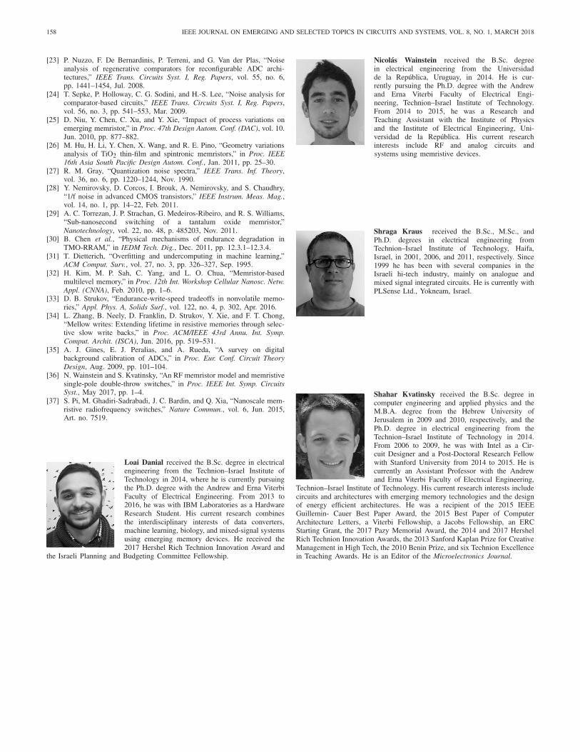
Nicolás Wainstein received the B.Sc. degreein electrical engineering from the Universidadde la República, Uruguay, in 2014. He is cur-rently pursuing the Ph.D. degree with the Andrewand Erna Viterbi Faculty of Electrical Engi-neering, Technion–Israel Institute of Technology.From 2014 to 2015, he was a Research andTeaching Assistant with the Institute of Physicsand the Institute of Electrical Engineering, Uni-versidad de la República. His current researchinterests include RF and analog circuits andsystems using memristive devices.
Shraga Kraus received the B.Sc., M.Sc., andPh.D. degrees in electrical engineering fromTechnion–Israel Institute of Technology, Haifa,Israel, in 2001, 2006, and 2011, respectively. Since1999 he has been with several companies in theIsraeli hi-tech industry, mainly on analogue andmixed signal integrated circuits. He is currently withPLSense Ltd., Yokneam, Israel.
Shahar Kvatinsky received the B.Sc. degree incomputer engineering and applied physics and theM.B.A. degree from the Hebrew University ofJerusalem in 2009 and 2010, respectively, and thePh.D. degree in electrical engineering from theTechnion–Israel Institute of Technology in 2014.From 2006 to 2009, he was with Intel as a Cir-cuit Designer and a Post-Doctoral Research Fellowwith Stanford University from 2014 to 2015. He iscurrently an Assistant Professor with the Andrewand Erna Viterbi Faculty of Electrical Engineering,
Technion–Israel Institute of Technology. His current research interests includecircuits and architectures with emerging memory technologies and the designof energy efficient architectures. He was a recipient of the 2015 IEEEGuillemin- Cauer Best Paper Award, the 2015 Best Paper of ComputerArchitecture Letters, a Viterbi Fellowship, a Jacobs Fellowship, an ERCStarting Grant, the 2017 Pazy Memorial Award, the 2014 and 2017 HershelRich Technion Innovation Awards, the 2013 Sanford Kaplan Prize for CreativeManagement in High Tech, the 2010 Benin Prize, and six Technion Excellencein Teaching Awards. He is an Editor of the Microelectronics Journal.

![DNL – Geography – London: A Global City - Freeaubel.free.fr/DNL/1re/LESSON_London_A_Global_City/LESSON_Londo… · 1/13 DNL – Geography – London: A Global City [CA v1.5] Summary](https://img.pdfslide.net/doc/110x75/5aa1a4f77f8b9aa0108c2368/dnl-geography-london-a-global-city-113-dnl-geography-london.jpg)