Embed Size (px)
Citation preview

//integras/b&h/Eer/Final_06-09-02/eerc015
15 Microprocessors
MIEEE
15.1 Introduction 15/3
15.2.1 15/5
15.3 15/6
15.4 15/8 15.4.1
15/8 15.4.2 15/9 15.4.3 15/9 15.5.4 15/10 15.4.5 15/11 15.4.6 15/11 15.4.7 Interrupts 15/13 15.4.8 Input/output 15/13 15.4.9 15/14
15.5 15/14 15.5.1 15/14 15.5.2 15/15 15.5.3 15/16 15.5.4 15/16 15.5.5 15/17
15.6 15/17 15.6.1 Selection 15/17 15.6.2 Repetition 15/18
15.7 15/19 15.7.1 15/19 15.7.2
15/19 15.7.3 15/20
15.8 15/21 15.8.1 15/21 15.8.2 15/21 15.8.3 15/22 15.8.4 15/23 15.8.5
15/23
15.9 15/23 15.9.1 15/23 15.9.2 15/24
D J Holding BSc(Eng), PhD, CEng, FIEE, MBCS,
Aston University
Contents
15.2 Structured design of programmable logic systems 15/3 Design for test
Microprogrammable systems
Programmable systems The logic design of a digital computer system Processor architecture Central processing unit Control and timing unit Arithmetic logic unit Memory unit
Microprocessors
Processor instruction sets Types of instruction Data objects and data types Instruction formats Addressing data objects Addressing program code
Program structures
Reduced instruction set computers (RISC) The reduced instruction set concept The reduced instruction set (RISC) processor Instruction pipelines
Software design Program development Assembly languages High-level languages Real-time processes Embedded real-time operating systems (RTOS)
Embedded systems Embedded processors System on chip (SoC) design

//integras/b&h/Eer/Final_06-09-02/eerc015

//integras/b&h/Eer/Final_06-09-02/eerc015
Introduction 15/3
15.1 Introduction
Digital systems are used to process discrete elements of information. They are built from digital electronic circuits that process discrete electrical signals using simple logic and arithmetic operations. A digital electronic system can also be used to hold or store discrete elements of information and this gives the system a memory capability. The ability to store information or data and to process the data by logical or arithmetic operations is central to the design of nearly all digital information-processing systems including digital computers. The function of a digital system is deter-mined by the sequence of operations that are performed on the information or data being processed. A digital system can be classified by the way in which its sequence of oper-ations is implemented.
A digital system is considered to be hardwired if the sequence of operations is governed by the physical intercon-nection of the digital processing elements. For example, in hardwired logic systems the physical interconnections of the elements govern the routes by which data flows between the processing elements and thus the sequence of processing operations performed on the data. Conventionally, a hard-wired system is considered to be inflexible because the design is specific to a particular processing function: if the pro-cessing function is changed, then the processing elements and their interconnections have to be altered.
The flexibility of hardwired systems has been much improved by the introduction of programmable (i.e. config-urable) logic devices such as Programmable Logic Arrays (PLAs) and Field Programmable Gate Arrays (FPGAs) that can be programmed or configured to implement an application-specific digital signal processing function. Flexibility has been improved further with the introduction of re-programmable (i.e. re-configurable) devices that can be reprogrammed easily during fast-prototype system devel-opment, and can be reprogrammed after a product has been deployed to provide enhanced features or performance. Progress in this area has been rapid and the latest genera-tion of re-programmable FPGA device can be configured with a wide variety of communication interfaces. This opens the possibility of using advanced communication technology, such as the Internet, to re-program or re-configure a remote hardwired system.
A digital system is considered to be genuinely program-mable if a prescriptive program of instructions (i.e. soft-ware) can be used to control the data-processing function of the system. This type of system usually incorporates a general-purpose processing element which is programmed to implement a specific function in a predetermined way. The coded instructions are normally stored in the memory part of the system and the program forms an integral part of the system. The ability to define the function of the digital system by programming introduces considerable flex-ibility into the system because the programming operation can take place after the general-purpose digital elements have been designed. It also means that identical hardware designs can be used in a number of different applications, the system being tailored to the individual tasks by the applica-tions program. A wide range of simple f unction ixed-fprogrammable systems, such as sequencers and micro-programmed controllers, are used as controllers in embedded electronic systems. In this type of application the sequence of instructions is usually held in read-only memory (i.e. firmware) which increases the robustness of the system.
The digital computer is a very important class of stored program system. The computer or microprocessor is distin-guished by the fact that its processing function depends on
both the prescriptive sequence of coded instructions and the value of the data being processed. In effect, the program prescribes a number of possible sequences of operations and the conditions under which they may be carried out. The computer, under program control, assesses the data and determines which specific sequence of instruction is to be executed. It is the ability of the computer to take into account the value of the data being processed, when taking decisions about the type of processing to be performed, which makes the computer such a significant and powerful information-processing device.
All three forms of digital electronic system find wide-spread application. Traditionally hardwired logic has been used extensively to provide the control and interface logic for more complex digital components such as micropro-cessors and other very large scale integration (VLSI) devices. It is also used in the design of high-speed signal processing circuits for FPGA implementation. Increasingly, hardwired logic is used to provide the interface circuits between the main functional components within a complex FPGA. Where flexibility is required, it is common to use reconfigur-able systems particularly in more complex applications.
Programmable systems are used in an extremely large range of applications. The simpler fixed-function program-mable systems are often used in repetitive tasks such as input scanning and data acquisition. They are also used in mass-produced products and as components of larger sys-tems such as telephony equipment. However, the continu-ally increasing computational power of the microprocessor and its derivatives, such as digital signal processing (DSP) devices or powerful reduced instruction set (RISC) proces-sors, has led to many of these applications being designed using fully programmable digital systems. In addition, commercial off-the-shelf (COTS) microprocessors are com-monly used in both stand-alone and embedded systems. Such systems are providing economic solutions to design problems in an increasingly wide range of application.
The increase in size of VLSI logic circuits has led to a new generation of reconfigurable devices that are large enough to contain a complete digital processing system within a chip, called System on Chip (SoC) devices. An SoC device can be configured to include an embedded digital RISC processor, memory, communication interfaces, clock man-agement, application-specific digital signal processing (hardwired logic functions), and appropriate internal inter-faces and data buses. This allows the designer to partition a design into those parts that will be implemented as software executing on the embedded processor and those parts that will be implemented in hardware as high-speed application-specific logic circuits. This design approach, known as co-design or co-ware, has the significant advantage that established and high-performance parts of the design can be committed to application-specific hardware, and more adventurous parts of the design or low-speed functions can be committed to easily changed software. This minimises risk, facilitates time-to-market which gives competitive advantage, and provides a good path to post-deployment upgrades of the system's capabilities and performance.
15.2 Structured design of programmable logic systems
The design of an application-specific digital system typically involves the so-called `top-down' approach and starts from a specification which includes a statement of the problem and the identification of the principal functional parts of
//integras/b&h/Eer/Final_06-09-02/eerc015
15/4 Microprocessors
the system. This can be elaborated as an architectural speci-fication which identifies the major components of the data or signal processing system and a control specification which describes an algorithm or procedure for the func-tional control of the processing system.
Traditionally a systems-level design approach is adopted and the design is developed through a structured process of elaboration and refinement. During this process, the data-or signal-processing specification is translated into a set of digital signal processing modules or circuits. Similarly, the control algorithm is depicted as a finite state machine (FSM) and is translated into a sequential logic circuit that generates the sequence of control signals which coordinate and synchronise the signal processing modules. In large designs the process of design refinement through analysis and decomposition can be applied repeatedly to form a hierarchy of functional descriptions. The process of decom-position is conventionally terminated when the granularity of the description matches that of commonly used digital electronic building blocks such as arithmetic circuits and memory elements, or sets of logic gates. However, modern programmable devices, such as complex programmable logic devices (CPLDs) and FPGAs, have complex internal structures that are purpose designed for the efficient imple-mentation of large functional units such as multipliers or ALUs. Therefore, it is often counter-productive to elabo-rate a design down to gate level without taking into account the logic structure of the target device. Figure 15.1 shows the general organisation of a system
designed using such an approach. It comprises external inputs and outputs, the controlled circuit which performs the data or signal processing, the controller which governs its behaviour, and internal signal paths which transfer con-dition or status information from the controlled circuit to the controller and control signals generated by the control-ler to the controlled circuit. The FSM controller is a simple sequential circuit that comprises: a state register which stores the current value of the state variables, combina-tional logic for generating the next value of the state vari-ables, a clock signal which synchronises the transition from the current state to the next state, and combinational logic for generating the value of the outputs (which are either a function of the current state or a function of the inputs and the current state).
Structured design techniques are well suited to computer-aided design (CAD) or electronic design automation (EDA) procedures. In particular, the hierarchical decomposition techniques used during the design phase have a one-to-one correspondence with the hierarchical CAD techniques used in traditional schematic diagram-based approaches to the capture, simulation, layout and routing, implementation, test and validation of complex circuit designs. Increasingly CAD tools provide high level specification capture facilities, such as graphical state machine (FSM) editors, to help capture design features in a tangible and user friendly manner.
The trend is to write the system specification using either a formal notation, or a programming language such as C or concurrent extensions of C, or a hardware descrip-tion language (HDL) such as VHDL or Verilog. These notations provide constructs that facilitate the description of complex logic systems or algorithms and an underlying mathematical structure that can be used to reason about the behaviour of the systems. The use of such abstract or high-level notations has been found to facilitate design by allowing the designer to focus attention on the functional aspects of the design without the need to bind the design to a particular implementation technology. This is supported by modern CAD tools that allow high-level behavioural specifications to be simulated to verify the function of the system (i.e. using symbolic simulation) before the high level description is compiled (i.e. synthesised) into a logic circuit. It is conventional to use the high-level description language to describe both the design (or unit-under-test) and a test-bench (test sequence generator and response analyser). Thus the highest level in the design hierarchy comprises both the design and a test-bench.
Design synthesis CAD tools are commonly used to trans-late high-level behavioural digital systems specifications into logic circuits. The synthesis process is not easy, and modern synthesis tools typically use artificial intelligence techniques and employ deep knowledge of the architecture of the FPGA in order to synthesise sensible, efficient and fast logic circuits. Once synthesised, the design can be incorporated into the conventional logic design process of post-synthesis simulation, routing, implementation, test and validation.
Conditional External (immediate) inputs
State outputs
FSM controller
outputs
Clock
Controlled circuit
Controlled circuit outputs
Figure 15.1 General organisation of a structured digital design

//integras/b&h/Eer/Final_06-09-02/eerc015
Structured design of programmable logic systems 15/5
15.2.1 Design for test
It is normally a principal design requirement that the circuit should be testable. In most structured design methods the derivation of the functional specification goes hand-in-hand with the specification of tests to verify that the designed circuit functions as intended. The problem of testing a cir-cuit is made more difficult when it is implemented as an ASIC because the limited number of pins on the integrated circuit restricts access to test points in the circuit. In parti-cular, the constraint that test inputs must be applied via the external input pins limits the controllability of internal parts of the circuit under test. Similarly, the constraint that the response of the circuit must be observed using the output pins limits the ability to observe the state of internal parts of the circuit under test. For testability, it is necessary to ensure that the accessible or primary inputs can drive each node of the circuit (the property of controllability) and that each node can be observed from the accessible or primary outputs (the property of observability).
Combinational logic is tested by applying a set of test patterns to the inputs of the circuit, measuring the circuit's response at its outputs, and comparing its response with its predefined fault-free function. In order to test a testable circuit, it is necessary to generate a set of inputs (test vectors) which can be applied to the primary inputs and drive each node of the circuit. Observability problems may arise if redundant logic to added to a circuit to provide hazard cover.
External Inputs A B
CLK / TCK
2:1 MUX1
0DQ
DQ 2:1 0
Scan In
Scan out
TDO
TDI
TMS D-type
D-type
Logic
NX0
NX1
State outputs
Conditional output logic
State output logic
outputs
Current States
X1 X0
MUX1
X1
Next State Next States
Clock
The problem of testing sequential logic is considerably more complex because the state of a sequential circuit is a function of both the current inputs and the previous state of the circuit. To reduce the problem of testing such circuits, it is desirable to open the feedback paths (which are essential to sequential behaviour) and thus change the problem to one of testing the constituent next-state and state-output combinational logic. This requires the introduction of addi-tional gates to inhibit the feedback paths, to allow the asser-tion of test states, to ensure the direct control of the clock, and to allow the observation of the next-state variables. This approach tests the combinational components and memory elements but does not provide a full-speed test of the actual sequential circuit and additional tests are required to ensure that the circuit is free of race hazards.
In the case of structured designs, a primary concern is the test of the controller which coordinates and synchronises the data or signal processing modules. In a typical FSM, the function of the controller is clearly defined by the con-trol algorithm and the finite state machine controller is rela-tively easily tested once the feedback loops of the sequential part of the circuit are opened. Furthermore, the state regis-ter can easily be reconfigured in the test mode to form a shift register for the entry of test data and the capture of test results. This is shown in Figure 15.2 for a controller with two state variables; the test mode select signal TMS causes the reconfiguration of the D-type state register to form a test vector shift register (shown in bold). This tech-nique, which is known as scan path testing, can be applied
Conditional
State register
Figure 15.2 Scan-path design for an FSM controller

//integras/b&h/Eer/Final_06-09-02/eerc015
15/6 Microprocessors
to a wide range of circuit and there are many variations of the theme, such as random scan and level sensitive scan techniques.
In general, significant increases in controllability and observability can be obtained if serial input and output techniques are used to load test data into an ASIC and remove capture response data from the ASIC. This can be achieved by incorporating a general-purpose shift register with serial-load/parallel-out, and parallel-load/serial-out facilities within the ASIC. In a typical test, the ASIC circuit would be put into test mode and the test stimuli or vector would be serial loaded into the shift register. The ASIC would then be switched into normal mode and the test
tdata present at the parallel output of the shif register would be allowed to excite the circuit. When the response had stabilised, observation data would be latched into the shift register using the parallel-load facility. The ASIC would then be put into test mode and the response would be output using the serial-output facility of the shift register. Clearly, the additional test circuits must be built into the ASIC as part of the design. This method requires up to five pins on the integrated circuit to be dedicated for test pur-poses: test mode select (TMS), serial test data in (TDI), serial test data out (TDO), direct control of the relevant clock circuits (TCK), and a reset (TRST). The use of such signals is consistent with the JTAG/IEEE standard 1149.1 which provides a framework for test at board and chip test level, primarily using the Boundary Scan technique that is commonly provided as a built-in component of modern VLSI and ASIC devices.
15.3 Microprogrammable systems
A typical digital system's design can be decomposed into a set of signal or data processing elements and a set of Finite State Machines (FSMs) which coordinate and control the signal- or data-flow and processing. To do this, the FSM controllers monitor any necessary signals (such as inputs or status signals) and generate the control signals necessary to coordinate, synchronise and control the signal- or data-processing elements. It follows that the FSMs form a crucial part of such designs, and a variety of structured design methods have been devised for capturing and synthesising the FSM controllers. These include traditional algorithmic state machine or ASM design methods, and state-transition diagram methods that allow direct synthesis of the design from Mealy or Moore diagrams. In addition, many HDL synthesis tools include program analysis tools that are designed to detect FSM-like structures and specifically synthesise FSM components. A key point in all these design methods is the assignment of a unique binary coding to each state of the system and the design of a bespoke finite state machine to generate the required state sequences and state outputs.
The need for bespoke hardware can be removed by designing a general-purpose controller (or finite state machine) which can be `programmed' to produce the neces-sary control functions. To accommodate such an approach, a simple FSM can be reduced to a networks of states, state outputs, and single-qualifier decisions by replacing any conditional or immediate outputs by state outputs and by inserting additional states where necessary to ensure that only one qualifier is associated with each decision. A unique state identifier is then assigned to each state according to a normal binary count (as far as possible) so that the state-machine design can then be implemented using a counter,
with appropriate controls, instead of with a state register and combinational next state logic. The modified FSM can then be reduced to a set of `instructions' by identifying commonly occurring structures and their associated counter control logic as follows:
(1) Sequence of states: increment counter unconditional (IUC).
(2) Decision: increment or branch conditional (IBC). (3) Wait until condition: hold or increment conditional
(HIC). (4) Branch unconditional: branch unconditional (BUC). (5) Loop forever: hold unconditional (HUC).
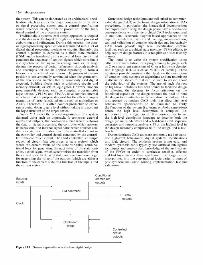
The counter is normally controlled using two control lines, `counter enable' (CE) and `counter load' (LD). On the next clock, the counter is incremented if CE is asserted or a branch address is loaded into the counter if LD is asserted. Thus, the counter control logic necessary for each construct or primitive instruction defined above can be readily determined. The use of mnemonics (such as IUC, HIC etc.) to represent commonly occurring structures allows the FSM to be replaced by a list of primitive sym-bolic `instructions'. Each instruction will define the present state identifier or location count, the mnemonic describing the control operation to be performed on the counter, the identity of any qualifier, the name or value of any branch address, and the name or value of the state outputs. A typ-ical instruction format is shown in Figure 15.3.
A suitable processing architecture for the above primitive instructions is shown in Figure 15.4. The state register is implemented with a controlled counter and, as only one instruction is needed per state, the input and output logic is efficiently implemented in ROM. The relevant input (or qualifier) for each state is chosen by addressing a multi-plexer. Before the contents of the ROM (or RAM) can be defined, each instruction must be assigned a binary code or `opcode' and each input must be assigned a MUX address. The instruction decoder is needed to translate the instruc-tions into suitable control signals for the counter. In the case of conditional instructions, the counter control signals depend on both the instruction type and the qualifier or `flag'.
Thus, each instruction stored in ROM comprises an opcode, the binary MUX address for the input qualifier, the binary branch-location address, and the binary values of the state outputs. This form of instruction is known as a microinstruction. The function of the controller can be changed by simply altering the microinstructions, and this process is known as microprogramming. Microprogramming is tedious and error prone and software development tools such as assembly language generators are often used to allow programming using symbolic notations.
In practice, a number of proprietary microprogrammable controllers have been developed. They are often equipped with a primitive stack to allow a limited procedure or sub-routine facility. This requires additional instructions such as `call procedure' or `branch to procedure' and `return from procedure' and mechanisms to increment the current counter (or ROM address) and save the incremented address in the stack, to load the procedure start address or value into
Figure 15.3 Microinstruction format
//integras/b&h/Eer/Final_06-09-02/eerc015
Microprogrammable systems 15/7
Figure 15.4 Simple microprogrammable architecture
Figure 15.5 Microprogrammable controller
//integras/b&h/Eer/Final_06-09-02/eerc015
15/8 Microprocessors
the counter, and to retrieve the address from the stack and load it into the counter. An external load facility for the counter may also be provided so that the controller can be used in conjunction with another processor. This gives the architecture shown in Figure 15.5. Such processors often have regularised instruction sets and well-developed tools for software development including simulation and emula-tion facilities.
Since a microprogrammed controller is a relatively simple circuit; designers have often taken the opportunity to incorporate a data processing capability into the design. Significantly, such microprogrammed `processors' often incorporate a specialised, very high performance, arithmetic processor. Typical examples include high performance floating-point arithmetic processors, and digital signal processing devices (which include a high-speed multiplier and accumulator for implementing the repetitive add-and-multiply operations found in digital filtering algorithms). Microprogrammed controllers are readily available as stand alone devices, or as pre-prepared HDL scripts, known as `intellectual property (IP) cores', that can be embedding within an HDL design and synthesised for an FPGA target.
15.4 Programmable systems
A programmable system, such as a microprocessor or com-puter, comprises a general-purpose processing unit which processes data or digital signals. The processing operations performed are specified by a computer program, which con-sists of a set of logical instructions stored in the computer memory.
A programmable system will comprise digital electronic circuits to:
(1) input signals or data from external circuits or systems; (2) move or transfer the data within the system; (3) store the data before, during and after processing; (4) process the data by logic, arithmetic or bit manipulation
operations; (5) output the processed data to external circuits or systems.
Each of these operations can be performed by an appro-priate configuration of combinational and sequential logic circuits including memory elements. In practice, program-mable systems comprise a general-purpose logic design which can be configured to perform a wide range of opera-tions. The hardware is controlled by a program or sequence of instruction codes which define the operations necessary to implement a particular processing function. The instruc-tion codes are normally stored in the memory part of the system and the function of the system can be changed simply by altering the stored program. This type of system can be considered to be composed of two parts: the hardware which is basically independent of the application and the software which defines the application function. Since the hardware part of such a system is invariant, it can be pro-duced economically as a standard design or device.
There are basically two types of general-purpose pro-grammable system. The fixed function programmable machine is a limited form of programmable system which is constrained to perform a prescribed and fixed sequence of instructions. This type of system does not have the capability under software control to select between two alternative sequences of instruction. A fixed function programmable machine is therefore forced to execute a
fixed sequence of instructions in all circumstances and is properly regarded as a programmed machine rather than a computer. The application function of such a system can be altered only by reprogramming the system. These systems can be used in any applications in which the processing function does not depend on the nature or value of the data being processed.
The digital computer is the most powerful and flexible form of programmable system. A program of instructions which are executed in sequence again defines its function, but in the case of the computer the program may specify alternative sequences of instructions and the conditions under which they can be executed. For example, conditional expressions and alternative sequences are implicit in high-level programming constructs such as `if condition-true then . . .', `repeat . . . until condition-true', and `while condi-tion-true do . . . '. Special hardware is required to carry out this type of operation and a computer is equipped with a logic circuit, known as a status register, which is used to store information about the status of the processor after it has executed an instruction. When a program is executed, each conditional expression is evaluated (using the actual values of the data variables) and the resulting values of the bits or flags in the status register are used to identify which alternative sequence of instructions is to be executed next. Thus, the order of processing may be modified according to the result of the instruction. It is this mechanism which allows a program to take into account the nature of the information being processed.
In effect, the computer can be programmed to take a decision about the future courses of action that it may take, based on the actual value of the data being processed. It is this facility which characterises a proper computing system and which makes the computer such a powerful data pro-cessing system. Such systems are providing economic solutions to digital signal and data processing problems in an increasingly wide range of applications.
15.4.1 The logic design of a digital computer system
A digital computer system can be considered to be com-posed of two logic structures. The first is associated with the flow, storage and processing of data and consists of the data input and output subsystems, the data highways used to move or transfer data within the system, the memory which is used to store the data, and the arithmetic logic unit which is used to process the data. The function of the processor is prescribed by a program of instructions held in memory. The second structure is responsible for controlling the fetching of instructions from memory and for ensuring that they are executed in the correct sequence. It also governs the detailed execution of each instruction and con-trols the data-flow and data-processing elements so that they perform the required processing operation.
The control structure consists of the memory which is used to store the program code and mechanisms for identi-fying the location of the next instruction, for fetching and decoding the instruction, and for identifying the location of any inputs or stored data which form the operands in a processing operation. It controls all aspects of the execution of the instruction including fetching operand data and, when necessary, taking into account the status of the pre-vious programming operation. It also identifies the destina-tion location of any resultand data generated by the processing operation and stores the resultand or generates an output.
The data-processing and program-control structures are heavily interconnected and often share common hardware.

//integras/b&h/Eer/Final_06-09-02/eerc015
Figure 15.6 Processor architecture
In particular, the program code and the data being processed are usually stored in an identical binary format. It is usual for code and data to be stored in separate areas or segments within a common memory unit.
15.4.2 Processor architecture
Computers and microprocessors are general-purpose programmable systems which perform sequential proces-sing operations. Classically, they are constructed using gen-eral-purpose functional units such as a central processing unit or CPU, a memory unit, and an input/output subsys-tem, as shown in Figure 15.6.
The CPU is the heart of the computer, it contains the control and timing unit (CTU) which controls the pro-grammed operation of the system and the arithmetic logic unit (ALU) which processes the data. An external clock
Programmable systems 15/9
provides the timing pulses or reference signals required by the CTU. The CPU also contains a number of important registers such as the program-counter which points to the next instruction, the instruction register which holds the current instruction, and the status register or flag register which stores the status information about the result of the previous instruction executed by the CPU.
The memory unit provides storage for program code and data. The code and data are always considered to be separate entities although they may share physical memory. (Some processor designs enforce the conceptual separation of code and data by providing separate memories for code and data.) The memory is arranged into words which con-sist of several binary digits, typically 8, 16 or 32 bits. Each word can be individually addressed and operated on by the computer.
The input/output subsystem of a computer provides the interface to external circuits or systems. Data may be passed in and out of the computer via serial or parallel interfaces. The input/output system is used to input program code, to input data for processing, and to output results. It also pro-vides the means of communication with the operator via a man-machine or human-computer interface (MMI or HCI). The processing power of the computer can only be used if the input/output subsystems allow efficient communication between the user or application and the processing system.
Many computer systems are configured around one or more general-purpose data highways. They typically con-sists of a common bus structure of address, data and control lines and are used to communicate to all devices external to the CPU including memory, input/output systems and backing stores. The simple bus-orientated architecture illu-strated in Figure 15.7 provides ease of access to the control, address and data highways which are used to interface any logical system to the CPU. Bus-oriented architectures are used in many designs to provide a flexible and easily expanded computer system.
15.4.3 Central processing unit
The CPU contains the CTU which coordinates, synchro-nises and controls the fetching of instructions from memory and the execution of the instructions. The execution of an instruction will typically involve fetching operand data from memory, processing the data in the ALU, and storing the result in memory. The CPU also contains at least the minimum set of internal registers necessary for the execu-tion of a program. These include the program-counter
Figure 15.7 Bus-orientated system architecture

//integras/b&h/Eer/Final_06-09-02/eerc015
15/10 Microprocessors
register, the instruction register, the data memory reference registers, and the CPU data registers.
15.4.3.1 Program-counter register
This holds the address of the memory location containing the next instruction to be executed. It is the programmer's responsibility to initialise the program-counter correctly, so that it points to the first instruction in the program. During program execution, the program-counter is automatically incremented by the CTU to point to the next instruction. In this way the CPU is forced to execute instructions in strict sequence. However, some instructions are provided which modify the contents of the program-counter. For example, unconditional jump, branch, or `go-to' instructions simply overwrite or modify the contents of the program-counter to effect a branch to another instruction. Similarly, conditional jump or branch instructions modify the con-tents of the program-counter if a particular condition is satisfied. This feature allows the program sequence to be modified if a specified condition is detected in the data being processed e.g. if the result of the previous instruction was negative.
15.4.3.2 Instruction register
This register holds the current instruction so that it can be decoded and input to the control and timing unit. Specifically, the instruction register holds the opcode which defines the type of instruction. Depending on the type of instruction, it may also hold immediate operand data or the addresses of operands and the address of the resultand. Since operand data and addresses comprise many bits, they are commonly held in temporary registers which can be considered as extensions to the instruction register. The contents of the instruction register can not be overwritten by the ALU, nor can they be accessed by a programmer.
15.4.3.3 Status register
This comprises a number of discrete status bits or flags and holds status data about the result of the previous instruction executed by the ALU. The data are used when computing `decisions', such as selecting one of two possible future courses of action. Processors actually compute decisions of this type in two stages. In the first stage the ALU computes the condition which governs the decision; the Boolean result (yes/no or true/false) is held in the status register. In the second stage, this result is used as a qualifier in a condi-tional operation, such as a conditional branch or jump, such that the value of the qualifier is used to choose the appropriate future sequence of instructions. It is the respon-sibility of the programmer (or compiler writer) to ensure the correct and consistent use of the status register throughout the two-stage process of computing a decision.
15.4.3.4 Data memory reference pointers
These registers hold the addresses of the operands and resultand and are loaded during the instruction `fetch'. They are used to access data objects during the execution phase of the instruction cycle and should be capable of accommodating the various addressing modes associated with the complex data types used in high-level program-ming languages. Therefore, it is perhaps more accurate to think of a data memory reference pointer as a mechanism which generates the address of a data object. The number of
address registers available in a CPU is an important feature of computer architecture. Ideally, separate pointers or mech-anisms are required for each operand and the resultand.
15.4.3.5 CPU data registers
These hold operands and resultand data during the execu-tion of a program. Again, microprocessors differ, particu-larly in the internal storage provided in the form of CPU data registers. However, most processors have an accumu-lator register into which the ALU will automatically load the resultand of a processing operation. Many modern microprocessors have a larger number of CPU data regis-ters which can operate as accumulators in complex arith-metic and logic operations.
Those parts of a processor which are of direct interest to a programmer are shown in the programmer's model which describes only those registers within the CPU which can be accessed by the programmer. Figure 15.8 shows the pro-grammer's model of a typical microprocessor system.
15.5.4 Control and timing unit
The basic operation of a computer or microprocessor is governed by the control and timing unit (CTU) which gen-erates the signals necessary to coordinate, synchronise and control the movement and processing of all information within the system. A simple external clock usually drives the unit, and this provides a time-reference signal from which the CTU generates the timing and control signals for the various logic subsystems in the computer. Modern high-performance processors may include a separate clock management subsystem which generates multi-phase timing sequences for use by the CTU.
The control and timing unit is responsible for controlling the main operational cycle of the processor which is known as the `instruction cycle'. The instruction cycle can be split
Figure 15.8 Programmer's model

//integras/b&h/Eer/Final_06-09-02/eerc015
into two distinct phases, the instruction fetch and the execu-tion of the instruction. During the instruction fetch the address of the next instruction is obtained from the pro-gram-counter mechanism and transferred to the memory address register (MAR). A memory reference operation is then performed on the code part or code segment of memory to read the opcode which is the first part of an instruc-tion. The opcode data are transferred via the memory buffer register (MBR) to the instruction register where it is decoded and then input to the CTU. The program-counter is then updated to point to the next part of the instruction or to the next instruction.
The opcode identifies any further memory reference operations which are required to complete the instruction `fetch'. The control unit uses the updated program counter to make reference to successive addresses in the code part of memory to fetch any further parts of the instruction, such as immediate data values or the addresses of the operands and the address of the resultand. This information is transferred to various temporary registers in the CPU for use during the `execute' cycle. At the end of the instruction `fetch', the CPU will contain all the information it requires to control the execution of the instruction and the program-counter will be pointing to the next instruction to be fetched (assum-ing that the execution cycle does not compute a new pro-gram-counter address). The various logic units used during the instruction `fetch' cycle are shown in Figure 15.9 in which the memory and input/output discriminator M/IO is used to distinguish between memory reference operations and any operations involving peripheral systems which may use the same address and data bus.
The opcode also defines the sequence of operations neces-sary to execute the instruction. During the execution part of the instruction cycle the control and timing unit will synchronise the transfer of data within the system and control the operation of the ALU. The control unit will access oper-and data by transferring the operand addresses from the temporary registers to the memory address register to perform memory reference operations. In practice, many processors have a complex data reference pointer which will compute the address of the data object using not only
Figure 15.9 Instruction `fetch' logic structure
Programmable systems 15/11
the temporary register but also base or segment registers, offset registers, and index registers according to the addressing mode specified in the instruction. If the computer has a memory-to-memory architecture, then operand data can be transferred direct from immediate access memory to the arithmetic logic unit and resultands can be returned direct to storage in immediate access memory. However, if the computer has a register-to-register architecture, then the operand data is normally transferred to a CPU register before being processed by the arithmetic logic unit and resultand data is held in the accumulator or transferred to another CPU register. The register-to-register architecture has distinct performance advantages, particularly when used with a multiple-instruction pipeline CTU, as in mod-ern reduced instruction set (RISC) processors.
15.4.5 Arithmetic logic unit
The actual data processing operations are performed by the ALU, which is a general-purpose logic system and can normally perform logical, arithmetic and bit manipulation operations. The ALU operates under the control of the control and timing unit and its function is defined by the current instruction held in the instruction register. The ALU can perform both monadic (single operand) and dyadic (two operand) operations and, therefore, has two input data paths. It generates status information in the status register and has an output data path for the resultand. Depending on the architecture of the processor, the oper-and data inputs may be from either immediate access mem-ory registers or CPU data registers. The resultand is usually output to a special register, known as the accumulator, which is normally a multi-function register which can parti-cipate fully in the processing operations. In some systems the accumulator is used to store one of the operands before a processing operation and is subsequently used to store the resultand. This technique removes the need to have two operand registers and may increase the operational speed of the processor. However, the need to minimise the number of CPU registers is no longer a major design objective and many modern microprocessors have a number of CPU regis-ters of advanced design which can act as operand registers or accumulators.
The ALU also contains the status register which is also known as a flag register or condition-code register. This regis-ter consists of a number of flip flops (flags) whose state reflects the result or state of the processing element at the end of the previous processing operation. This is illustrated in Figure 15.10 which shows in schematic form the structure of a typical ALU and the other logical systems associated with the execution part of the instruction cycle.
15.4.6 Memory unit
The memory unit provides storage for program code and data. Computers commonly use two types of memory, fast immediate-access memory and backing store memory, which have different roles and functions.
The immediate-access memory is considered to be the primary memory unit of a computer, it is used to store program code and the data associated with the program so that it may be readily accessed during the execution of the program. Read only memory (ROM) devices may be used to store information which does not alter, such as program code or constant data, and random-access read-write memory (RAM) devices are used to store data which may be altered, such as the value of variables. The immediate

//integras/b&h/Eer/Final_06-09-02/eerc015
15/12 Microprocessors
Figure 15.10 Instruction `execution' logic structure
access memory is normally constructed using semiconduc-tor memory devices. Typically, large memories are built using dynamic RAM memory devices which provide `high-density' storage at relatively low cost.
The immediate-access memory is normally limited in size by the computer architecture. For example, simple micro-processors may have a 16-bit memory address and this limits the size of the immediate-access memory to 64k registers or elements. While a 64 k �( 8-bit memory is often sufficient for embedded applications such as dedicated control systems, larger memories are often required to support general-purpose applications software. Typically, modern microprocessors use 32-bit effective memory addressing and commonly have a 128 M byte or 256 M byte memory which is sufficient to run modern operating systems and
applications software. However, the performance of memory-intensive applications, such as image processing, computer aided design (CAD), and interactive computer games, may benefit from larger memories. Therefore, more advanced microprocessors have the capability to physically address 1 G or more of memory.
Many computers have facilities for using an area of mem-ory as a stack. This is a block of RAM memory which is used on a last-in/first-out (LIFO) basis for storing context information, such as the values of the program-counter, status register, and other CPU registers, or for storing data such as the parameters passed to subroutines. This facility is particularly useful for storing addresses and register con-tents during subroutine operations or during the context switches which take place following an interrupt.
//integras/b&h/Eer/Final_06-09-02/eerc015
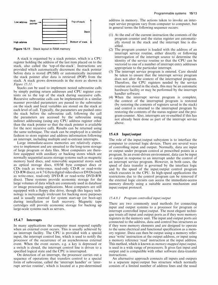
Figure 15.11 Stack layout in RAM memory
A stack is organised by a stack pointer, which is a CPU register holding the address of the last item placed on to the stack, also called the `top-of-the-stack'. Instructions are provided which automatically decrement the stack pointer before data is stored (PUSH) or automatically increment the stack pointer after data is retrieved (POP) from the stack. A stack grows downwards in the store as shown in Figure 15.11.
Stacks can be used to implement nested subroutine calls by simply putting return addresses and CPU register con-tents on to the top of the stack during successive calls. Recursive subroutine calls can be implemented in a similar manner provided parameters are passed to the subroutine on the stack and local variables are stored on the stack at each level of call. Typically, the parameters are pushed onto the stack before the subroutine call; following the call the parameters are accessed by the subroutine using indirect addressing (using any CPU address register other than the stack pointer so that the stack pointer is available for the next recursive call). Results can be returned using the same technique. The stack can be employed in a similar fashion to store register and address information following an interrupt, including multiple and re-entrant interrupts.
Large immediate-access memories are relatively expen-sive to implement and are unsuited to the long-term storage of large program or data files. Most computers are there-fore equipped with auxiliary or backing stores which are normally sequential access storage systems such as magnetic memory hard discs, and removable sequential stores such as optical storage discs, 650 M byte compact discs or CDs (such as write-once, read-only CD-R or read-write CD-RW discs), or 4.7 G byte digital video discs or DVDs (such as write-once, read-only DVD-R or read-write DVD-RW discs). These systems provide economic storage for the large volumes of data which are commonly used in database or image processing applications. Most computers are still equipped with a floppy disc drive, though this legacy tech-nology is increasingly irrelevant for backing store purposes and is usually reserved for system start-up (or boot-up) during installation or fault recovery. Magnetic tape cartridges still provide economic storage for backing up large-scale systems such as servers.
15.4.7 Interrupts
In many applications the computer must respond rapidly when an external event occurs. This is usually achieved by an interrupt facility. The CPU is provided with a special input, the interrupt control line, which is used to notify the processor of the occurrence of an asynchronous external event. When the event occurs, e.g. a key is depressed or a switch is closed, the interrupt control line is driven to a specified logical state and the CPU is interrupted.
On detection of an interrupt, the processor carries out a sequence of operations that transfers control to a special form of subroutine, called the `interrupt handler' or `inter-rupt service routine', which is located at a pre-determined
Programmable systems 15/13
address in memory. The actions taken to invoke an inter-rupt service program vary from computer to computer, but in general terms the following sequence occurs:
(1) At the end of the current instruction the contents of the program counter and the status register are automatic-ally stored in the stack and the interrupt line is dis-abled.
(2) The program counter is loaded with the address of an interrupt service routine, either directly or following interrogation of the interrupt source to determine the identity of the service routine so that the CPU can be vectored to one of a number of interrupt entry addresses appropriate to the particular interrupt.
(3) The interrupt service program is entered. Care should be taken to ensure that the interrupt service program does not alter the context of the interrupted program. Therefore, the CPU registers needed by the service routine are stored in the stack, this may be an automatic hardware facility or may be performed by the interrupt handler software.
(4) When the interrupt service program is complete, the context of the interrupted program is restored (by restoring the contents of registers saved in the stack) and control is returned to the interrupted program by restoring the contents of the status register and the pro-gram-counter. Also, interrupts are re-enabled if this has not already been done as part of the interrupt service above.
15.4.8 Input/output
The role of the input/output subsystem is to interface the computer to external logic devices. There are several ways of controlling input and output. Normally, data are input or output under program control at prescribed points in a program. In an event-driven environment, data can be input or output in response to an interrupt under the control of an interrupt service program. However, in both cases, the speed of data transfer is governed by the interface logic and by the speed of the input/output control program which executes in the CPU. In high-speed applications the restrictions due to the control program can be removed if the external logic circuits can access the immediate-access memory directly using a suitable access mechanism and input/output protocol.
15.4.8.1 Program controlled input/output
There are two commonly used methods for connecting input and output systems to a processor for program or interrupt controlled input/output. The most elegant techni-que treats all input and output ports as if they were memory registers in the memory unit. The input and output ports are connected to the address, data and control bus structures as if they were memory elements and are designed to operate to the same electrical and functional specification as a mem-ory register. Data can then be output using a memory refer-ence `write' instruction at the output address, or input using a memory reference `read' instruction at the input address. This method, which is known as memory-mapped input/output, is used in a wide range of processors. It gives fast input and output and is compatible with other software data-transfer instructions.
An alternative approach connects all inputs and outputs to a separate input/output bus structure which normally consists of a limited number of address lines and the usual

//integras/b&h/Eer/Final_06-09-02/eerc015
15/14 Microprocessors
control signals. In bus-orientated systems a subset of the memory address lines is used and an additional memory or input/output discriminator signal (M0/IO) is used to gener-ate unambiguous addresses. Input/output-mapped input/ output is not compatible with memory reference operations and special instructions such as IN or OUT are often used to distinguish this mode of operation.
Serial communications are usually interfaced using a universal asynchronous receiver and transmitter device (USART) which contains a serial-to-parallel receiver buffer, a parallel-to-serial transmitter buffer, a mode control regis-ter, and a status register which indicates valid communica-tions. The data, control, and status register are accessed using either memory-mapped or input±output mapped techniques according to the architecture of the processor.
15.4.8.2 Interrupt-driven input/output
An interrupt can be used to force a processor to suspend its current task and execute an interrupt service program, as described in Section 15.4.7. Interrupt driven input/output is implemented by connecting the control logic of the exter-nal device to an interrupt line so that the device can demand the CPU's attention. Following the generation of an inter-rupt, the CPU is forced to respond immediately and execute a program which services the input or output requirements of the interrupting device. Interrupt-driven input/output maximises the utilisation of the external device, but causes suspension of the current task. Interrupt-driven input/out-put is commonly used to interface intermittent inputs such as keyboards. However, in some embedded applications it is undesirable to interrupt an executing task, and the preferred approach is to regularly inspect (or poll) an external device for the availability of an input.
15.4.8.3 Direct memory access
The use of direct memory access (DMA) allows an external device to transmit data directly into the computer memory without involving the CPU. The CPU is provided with con-trol facilities which allow the DMA controller (external to the CPU) to gain control of the CPU data bus. The DMA controller must provide a memory address, the data, and bus control signals to effect a data transfer. The DMA con-troller then transfers data directly over the bus to or from the memory. DMA transfers are commonly used to send blocks of data, rather than individual items of data, between backing stores or peripheral devices and memory. The controller contains a counter to increment the memory address and count the number of transfers made within the data block. The DMA process is also referred to as cycle-stealing, since it proceeds simultaneously with program execution, the only effect being that the instruction execu-tion time is increased by the number of memory cycles used when a transfer is in progress.
The relative merits of DMA over other means of input/ output is that it is fast, uses the minimum amount of computer time per data word transferred and operates autonomously. The loss of instruction execution time is not usually significant unless a very large number of devices are under DMA control. The major disadvantage of DMA is that the computer program is not explicitly aware of changes in data or the completion of a DMA transfer and it is usually necessary to make the DMA controller invoke an interrupt to inform the CPU that a data block transfer is complete.
15.4.9 Microprocessors
Advances in microelectronics and computing science have provided the technologies necessary to construct the com-plete central processing unit of a computer on a single inte-grated circuit; this device was called a microprocessor. The microprocessor, which was developed in 1971, realised a step change in the cost, performance, power consumption and reliability of a minimum computer system. Further advances in VLSI design led to the development of integrated circuits containing both the CPU and the memory unit; the so-called single chip computer. In effect, these advances had resulted in the miniaturisation of the computer.
The microprocessor can also be viewed as an advanced programmable logic device. Special microprocessors and other advanced programmable systems have been devel-oped to carry out specific computational functions. These processors are often designed to work in conjunction with a general CPU and are known as co-processors. A number of devices such as fast floating-point arithmetic units, com-munication or local area network co-processors, and multi-media units such as audio processors and graphics and video display generators, are available and can be used in the design of powerful processor architectures. To prevent such high-bandwidth processing elements making signifi-cant demands on immediate-access memory, they are often provided with separate application-specific memories as in the case of video display subsystems. A typical system archi-tecture of this type is shown in Figure 15.12 which illustrates the use of programmable systems including microprocessors in the design of an advanced information processing system.
15.5 Processor instruction sets
Most general-purpose computers or microprocessors are designed to execute sequences of instructions or more com-plex programs of instructions which prescribe the actions necessary to input, store, and process data, and output com-puted results. The instruction set of a processor defines the machine code operations, which the processor can perform. However, the range of instructions available with a particu-lar processor depends to a considerable extent on the design objectives of the particular manufacturer. The range and capability of the instruction set provided may have a con-siderable influence on the choice of a computer for a parti-cular application task.
15.5.1 Types of instruction
Although there is no standardisation of computer instruc-tions, most processors provide primitive operations or instructions for the following.
15.5.1.1 Program flow control
The sequence in which instructions are executed is defined implicitly by the program which comprises an ordered list of instructions held in successive memory locations. Unconditional branch or jump instructions can be used to jump to a program in another part of memory. Also, repeti-tive or loop structures can be formed by jumping back to an instruction which has already been processed. However, the true power of a programmable system is provided by conditional instructions. The flags in the status register can be used as qualifiers for conditional branches, either on their own, as in `branch if zero', or in combinations as in `branch if greater than' or `branch if less than or equal'.

//integras/b&h/Eer/Final_06-09-02/eerc015
Processor instruction sets 15/15
Immediate access Backing memory stores Peripherals
CPU M controller
co-processorco-processor
Disc controller
LAN co-processorco-processor
Bus timing and control
controller emory
Video display Arithmetic Audio
Serial and parallel port
Multimedia display systems
Figure 15.12 A multiprocessor system architecture
When computing decisions (selecting between alternative sequences of code) conditional branch or jump instructions are used to determine whether to continue the present sequence or jump to the start of an alternative sequence. Similarly, conditional jumps can be used to form condi-tional exits from repetitive structures.
Although most processors are unable to implement directly the flow control constructs found in high-level pro-gramming languages, the implicit sequence, unconditional branch and conditional branch instructions form the primi-tives from which constructs such as `if-then-else', `while-do', and `repeat-until' can be formed.
15.5.1.2 Data-flow including input and output
Data-transfer instructions, such as MOVE, can be used to input external data to a CPU data register or an immediate-access memory register, to transfer data between such regis-ters, and to output data from such registers to the outside world. Although these instructions do not necessarily make use of the ALU and may not alter the status register, they can be classed as data processing instructions in the sense that they assign values to the variables (registers).
15.5.1.3 Data-processing instructions involving the ALU
Most processors provide a range of arithmetic instructions including addition, subtraction, multiplication and division. These instructions are used in mathematical applications including the data `sorting' operations used in data base applications. Simple processors often implement these operations using two's complement integer arithmetic. More complex algorithms involving floating point arith-metic can be programmed using these primitive operations. However, these programs often make intensive use of the processor and are relatively slow and it is common to enhance the performance of such processors by adding arithmetic co-processors. More advanced processors have
System control, address and data bus
Communication networks
powerful built-in arithmetic capabilities including floating point arithmetic units.
Most processors can also implement logic operations such as NOT, AND, OR, and EXCLUSIVE OR (XOR) which are implemented `bit-wise' by performing the opera-tion simultaneously on each corresponding pair of bits in the operands. These operations are used to perform the `compare' or `find' operations used in database applica-tions. Many processors can also implement shift/rotate instructions which involve moving all the bits in a computer word either to the right or the left. There are several pos-sible form of shift, such as arithmetic and logical shifts and logical rotations. (Few conventional high-level languages give direct access to primitives for physical bit-level mani-pulation.)
15.5.1.4 Machine control
These instructions control the mode of operation of the processor. Many machine control instructions, such as START/RESTART, HALT, STOP have a profound influ-ence on the behaviour of the processor. Similarly, in event driven systems, machine control instructions such as INTERRUPT ENABLE/DISABLE and interrupt priority control instructions affect the ability of the processor to respond to external stimuli. Therefore, some processors classify certain machine control instructions as `privileged instructions' which can only be used if the processor is in a special `systems' or `supervisor' mode that is used by systems programmers. (Few conventional high-level programming languages give direct access to machine-level primitives for machine or interrupt control.)
15.5.2 Data objects and data types
At machine level textual, numerical and logical information is represented by codes of binary digits and the processor in not able to infer the context of any particular binary data

//integras/b&h/Eer/Final_06-09-02/eerc015
15/16 Microprocessors
object. Thus, the concept of data typing, in the high-level sense, does not exist at machine level.
A processor handles such data in terms of the contents of registers. Thus low-level primitive instructions transfer and process data by reference to the architecture and registers of the processor, such as input/output device registers, CPU data registers and/or accumulators, and immediate-access memory registers. Data typing at machine level is restricted to specifying the length of a data object. Most low-level assembly languages provide assembler directives which allow the programmer to declare data objects by length, assign symbolic names (identifiers) to the objects, and provide initialising values for variables. When an assembly language source program is translated into machine code, the assembler enforces the data-type rules on the usage of the declared data objects and allocates storage space at machine level for all data objects.
Although limiting, low-level data types provide the build-ing blocks for accommodating (storing and processing) the more complex data types normally associated with high-level programming languages. However, the efficient use of high-level data types also depends on the availability of suit-able addressing mechanisms for accessing data objects.
15.5.3 Instruction formats
Each computer instruction is stored in memory as binary numbers and can be considered to comprise a number of fields:
(1) Operation code (op-code): this part of the instruction identifies the type of operation which is to be performed (such as `add' or `jump'), the number and addressing mode of the operands, and the addressing mode of the resultand (if any).
(2) Operand field: this specifies either an immediate data value (if immediate addressing) or the address of the operand on which the instruction operation is to be performed. The processor's data memory reference mechanism will use the address information in conjunc-tion with the addressing mode to compute the effective address (physical address) of the operand.
(3) Resultand field: this specifies the address of the result-and (corresponding to the addressing mode used). In some processors, the resultand address is, by default, the same as that of one of the operands, and when the instruction is executed the resultand overwrites the operand concerned.
The format of a typical instruction, such as ADD, for a memory-to-memory architecture processor in which the operands and resultands reside in immediate access memory is shown in Figure 15.13. This type of instruction format has the potential to generate multi-word instructions. For example, a 16-bit microprocessor may have a 16-bit op-code and either a 16, 20, 24 or 32 bit memory addressing capability. The resulting instruction would be long and the corresponding instruction fetch would require many memory reference operations, which is inefficient. Many CPU archi-tectures force the resultand to overwrite one of the oper-ands, this gives some gain in efficiency since the resultand address is, implicitly, the same as one of the operands. The format of a typical instruction of this type is shown in Figure 15.14.
In practice, many processors have a register-to-register architecture where the operands and resultands are stored in CPU data registers, which being few in number can be
Figure 15.13 Instruction formatÐexplicit resultand
Figure 15.14 Instruction formatÐimplicit resultand
addressed using very short direct addresses. This gives some gain in efficiency, although separate MOVE instruc-tions are required to load data from memory into the CPU registers (the LOAD operations) and to return results to memory (the STORE operation). The so-called LOAD-STORE architecture, or register-to-register architecture processor, is the default architecture for modern reduced instruction set (RISC) processors. These processors commonly have a CPU register file comprising 32 general-purpose 32-bits registers that can act as source registers for operands and accumulators for resultands.
15.5.4 Addressing data objects
During the execution of an instruction, operands are fetched from the addresses indicated in the operand field of the instruction, and resultands are returned to the address shown in the resultand field of the instruction. A number of different methods of addressing operands have been devel-oped. These address modes are used to introduce flexibility by decoupling the logical address from the physical address, to extend the address range of the memory that can be accessed from an instruction, and to provide support at a primitive level for the addressing mechanisms required in advanced data structures. The data-memory reference sys-tem is used to generate the physical address of a data object from knowledge of the addressing mode and the values in the operand field of the instruction and any associated address registers.
The address modes commonly encountered for accessing operands are as follows.
15.5.4.1 Immediate addressing
In this mode, the actual value of the operand is included in the instruction, i.e. the operand address field is a literal. This allows rapid access to the operand, but the value of the operand is fixed by the program code. The operand may be a data object, such as an integer constant, or an address object. Typically, it is used to load small integer constants into a register. (To avoid repeatedly using immediate addressing to load the commonly used value zero into CPU registers, many RISC processors have one CPU `register' permanently hardwired to the value zero.)
15.5.4.2 Direct addressing
In this mode the value in the operand address field is the address of the operand. There are two main variants of direct addressing. In CPU register direct addressing the address of the CPU register is given, as an explicit value,

//integras/b&h/Eer/Final_06-09-02/eerc015
in the address field of the instruction. Since most CPUs have a small number of CPU registers, the address field is restricted and this allows single word instructions. CPU Register direct addressing is fast because the instruction is short and the operands are already held in the CPU. It is used extensively in register-to-register architecture proces-sors, including RISC processors. In memory direct address-ing the immediate access memory address of the operand is given, as an explicit value, in the address field of the instruction. In limited-word-length computers this means that only a small area of memory can be assessed directly. Also, this addressing mode is inflexible because the address is embedded in the program code. It is commonly used to access address constants, such as input/output ports.
15.5.4.3 Indirect addressing
In this mode, the operand field of the instruction identifies an address register (usually a CPU register) which holds the address of the operand. The address register must be initial-ised before use. In effect, the address-register acts as a `pointer' to the operand. This removes the need for the instruction to specify the absolute address, which introduces flexibility. It also allows the operand to be accessed by a one-word instruction. If the address register has accumula-tor capabilities and can participate in arithmetic operations, then the indirect address or pointer can be manipulated to give access to complex data structures. For example, the indirect address could be incremented during successive passes through a loop of instructions.
Some processors have special mechanisms which allow an indirect register to be decremented or incremented immedi-ately before use (e.g. pre-decrement) or immediately follow-ing use (e.g. post-increment). Such pointers can be used as stack pointers which are automatically updated to point to the `top-of-stack' following a PUSH or POP operation.
15.5.4.4 Indexed addressing
Indexing is used to address sequential data structures. The effective address of a data object in the structure is formed from the sum of two components; the address of (the start of) the data structure and the index or offset of the object relative to the start of the structure. The data-memory refer-ence mechanism computes the effective address as the instruction is executed.
Indexed addressing is normally implemented using two CPU registers. An address-register is used (as in indirect addressing) to point to the start of the data structure (the address of the first object the structure) and a second regis-ter, known as the index register, holds the offset address of the data object. The index register usually has an accumula-tor capability such that the index can be readily modified or incremented. Modern processors often have a number of address registers which can be used as pointers to data structures and a number of index registers. An indexed addressing instruction for such a processor would specify both the pointer and index register.
15.5.4.5 Base and (relative) offset addressing
In this system of addressing, an address register is used as a `base pointer' and points to the segment of memory allo-cated to the data associated with a program. All references to data objects are made relative to the base address. The data memory reference mechanism automatically adds the
Program structures 15/17
base address of data segment when calculating the effective address of a data object. Thus, in this system, direct addresses, indirect address, and indexed addresses are assumed to be relative to the base address. Thus all relative addresses associated with the operand data can be calcu-lated when the program is compiled or assembled and do not require further alteration when the program is located. This has the significant advantage that, as far as references to data objects are concerned, the data segment can be relocated easily because the executable program code remains unchanged and only the value of the base pointer has to be altered.
15.5.5 Addressing program code
The program-counter points to the location of the current instruction and is incremented as each instruction is executed in sequence. However, the value in the program-counter is overwritten during unconditional and con-ditional branch or jump instructions. In effect, the operand of branch and jump instructions may modify the value of the program counter. Branch and jump instructions employ a variety of addressing modes:
15.5.5.1 Direct addressing
The value in the operand field of the instruction is the desti-nation address of the branch or jump.
15.5.5.2 Indirect addressing
The operand field of the instruction identifies an address-register which holds the destination address of the branch or jump.
15.5.5.3 Relative addressing
The value in the operand field is interpreted as a positive or negative binary number which is added to the current con-tents of the program-counter to determine the destination address of the branch or jump. This is usually quite efficient because most destination addresses will be fairly close to the instruction being executed. Since the offset of the relative address is independent of the location of the code, the offset can be determined as a constant when the program is assembled or compiled and does not need to be altered when the program is located. This has the significant advan-tage that, as far as references to code locations are concerned, the executable program code can be relocated and only the initial value of the program counter has to be changed.
15.6 Program structures
Certain program structures occur so frequently in program design that it is worth looking at methods for implementing them both at high-level and at assembly or machine level. The implementations use both unconditional and condi-tional jumps.
15.6.1 Selection
The `if-then-else' selective construct is used to select between two alternative instructions (or processes). This high-level

//integras/b&h/Eer/Final_06-09-02/eerc015
15/18 Microprocessors
construct specifies the alternative processes and the condi-tions under which they can be executed, for example:
if x > 0 then P1 else P2;
The decision part of this construct is implemented at machine level by two distinct instructions:
(1) the evaluation of the conditional expression, which must be a relational operation that returns a Boolean result. When this is computed, the result is reflected by the setting or resetting of one or more flags in the ALU status register.
(2) the conditional branch which uses the relevant flags in the status register as operands. When the conditional branch instruction is executed it passes program flow control to the selected process (i.e. if the condition is true then branch to P1 else continue with P2). Note that in the low level implementation an unconditional branch instruction has to be inserted at the end of the `else process' P2 to allow both alternative processes to be stored in sequential memory, as shown in Figure 15.15.
15.6.2 Repetition
Consider a process which must be executed several times. If the number of iterations is known, then a `for' loop would be indicated; otherwise the loop structure could be imple-mented using either as a `while . . . do' or a `repeat . . . until' construct. The `repeat . . . until' construct should be used if the process is to be executed at least once, otherwise the `while . . . do' construct, which allows the possibility of an exit before the process is executed, should be used. Since both the `for' and `repeat . . . until' constructs can be derived from the `while . . . do' construct, the `while . . . do' construct is
the primitive and is found in all high-level sequential and concurrent programming languages.
15.6.2.1 `Repeat-until' construct
This repetitive construct allows a process to be executed at least once. The number of times the process is executed depends on a value of a control variable, for example:
count : �(number; repeat
P1 until count <& 0 do ;
where the process P1 must update the loop control variable, as in:
count : �(count �1;
Implementation of the `repeat-until' construct at low-level requires an explicit loop control mechanism, with initi-alisation and termination phases. The `repeat-until' construct tests the exit condition at the end of the loop as shown in Figure 15.16.
15.6.2.2 `While-do' construct
This construct provides for a process not to be executed, or to be executed one or more times. The number of times the process is executed depends on a value of a control variable, for example:
count : �(number; while count >&�(0 do
P1;
Figure 15.15 `If-then-else' construct Figure 15.16 `Repeat-until' construct

//integras/b&h/Eer/Final_06-09-02/eerc015
Figure 15.17 `While-do' construct
where the process P1 must update the loop control variable, as in:
count : �(count �1;
Implementation of the `while-do' construct at low-level requires an explicit loop control mechanism, with initial-isation and termination phases. The terminating condition must be evaluated at the start of the loop. The general form of the `while-do' construct is shown in Figure 15.17.
15.7 Reduced instruction set computers (RISC)
15.7.1 The reduced instruction set concept
The evolution in processor design during the 1980s and early 1990s led to increasingly complex processor architec-tures. The emerging 32-bit architectures accommodated a good range of data types and a wide range of instruction types and addressing modes. In addition, the flexible instructions often allowed the user a free choice of the addressing mode for the operands which resulted in many permutations of (variable-length) instructions. Such pro-cessors were characterised by the complexity of their instruction sets, the complex sequences necessary to `fetch' the variable-length instructions, and the complex and very large instruction-decode logic. These processors were known as complex instruction set computers (CISC) processors.
Analysis of the actual use of these processors showed that the instruction set complexity often exceeded the needs of
Reduced instruction set computers (RISC) 15/19
many applications. Many users simply preferred to use a familiar and well understood subset of the data types, addressing modes, and instructions. In addition, it was found that common programming constructs, such as con-ditional expressions, were often formed using simple rela-tional operations, such as `equals' and simple and short constants, such as `zero'. Similarly, program branches often had a short relative offset that could be accommo-dated using short (16-bit) relative addressing. This led to the notion of developing high-performance processors with a reduced set of appropriate instructions.
15.7.2 The reduced instruction set (RISC) processor
The reduced instruction set computer (RISC) processor has a relatively simple register-to-register architecture which focuses on a CPU register file of, say, 32 general purpose 32-bit registers. Each register may hold data or addresses and can provide source operands and/or act as an accumu-lator for resultands. Since data can not be transferred directly between immediate-access memory and the ALU, simple data transfer (LOAD) instructions are used to trans-fer operand data from immediate-access memory to CPU registers so that it can be processed subsequently by the ALU. Similarly, simple data transfer (STORE) instructions must be used to transfer result data from CPU registers to immediate-access memory. Thus, if X, Y, and Z are stored in immediate-access memory, the high level expression X: �(Y �Z must be implemented using four separate instructions.
R1: �(Y LOAD operation, load CPU register R1 with Y from memory
R2 �(Z LOAD operation, load CPU register R2 with Z from memory
R3 �(R1 �R2 ALU operation, write into CPU register R3 sum R1 �R2
X: �(R3 STORE operation, store CPU register R1 as X in memory.
The apparent disadvantage of using four low-level instruc-tions to implement one higher-level memory-to-memory instruction is partially offset by the simple format of the RISC instructions. Register-to-register architecture pro-cessors have relatively short instructions since there is at most only one immediate-access memory reference opera-tion (to load or store an operand) per instruction. This leads to the notion of using fixed-length instructions. A typical 32-bit RISC processor with 32 CPU registers will use a 32-bit fixed length instruction with, say, a 6-bit op-code, 5-bit direct addressing of CPU registers, and relative (base and offset) addressing of immediate-access memory using 16-bit relative addresses or immediate data. Thus LOAD and STORE instructions may consist of the 6-bit op-code, a 5-bit CPU register address for the operand or resultand, and an immediate-access memory address comprising a 5-bit base (register) address and a 16-bit rela-tive offset. Similarly, an ALU instruction may comprise the 6-bit op-code, and either three 5-bit CPU register addresses (plus scope for instruction extensions), or two 5-bit CPU register addresses and a 16-bit immediate-data object. The use of a 32-bit instruction, which can be `fetched' in a single memory reference operation, results in a fast instruction cycle and much simplified instruction decoder logic. The performance of RISC processors is further enhanced by the use of multi-stage instruction-pipelines.

//integras/b&h/Eer/Final_06-09-02/eerc015
15/20 Microprocessors
Counter Unit
Immediate-access data
CPU Register file
ALU
address calculation
Immediate-access
ALU status flags
Register
Op-code
Program
memory
Branch instruction memory
1ST STAGE 2ND STAGE 3RD STAGE 4TH STAGE 5TH STAGE
Instruction Buffer
Op-code, Op code, - Op code, - Op code, -operand or operands, Load operand Store operand resultand operand or or ALU resultand, or ALU resultand, addresses, resultand operand or operand or or immediate data address, resultand address resultand address or address or immediate data
or addess
Figure 15.18 Simplified instruction pipeline
15.7.3 Instruction pipelines
The conventional instruction `fetch' and `execute' cycle imposes speed constraints on a processor. The primary pro-blem is the time taken to access immediate-access memory, both to `fetch' the instruction and to read operands during LOAD instructions, or to write operands during STORE instructions. In each case the processor ALU is idle (not processing data) while the memory reference operation is taking place. This limitation can be overcome, to a large extent, by the notion of pipelining.
The basic idea of pipelining is to partition the processor into autonomous operational or functional units that can operate concurrently, (such as instruction `fetch' from immediate-access memory, program counter update, CPU register-file read, ALU operation, write operation on immediate-access data memory, read operation on immedi-ate-access memory read, CPU register-file write). Typically, this allows the process of `fetching', decoding and executing an instruction to be split into the following stages.
(1) Instruction `fetch' and program counter update. (2) Operand read from CPU register file. (3) ALU operation or effective address calculation (for
LOAD and STORE). (4) Immediate-access data memory read (for LOAD)
or write (for STORE). (5) Resultand (ALU operations) or operand (for LOAD)
write to CPU register file.
In effect, the traditional instruction register is replaced by a pipeline of instruction buffers each of which store the infor-mation (opcode, CPU register addresses, memory reference address, operands, resultands, ALU status) necessary to carry out subsequent phases of the instruction cycle for each instruction, Figure 15.18. Thus, such a pipeline will normally contain five sequential instructions, and each stage of the pipeline will have the information and resources required to autonomously implement its stage of the instruction cycle. In addition, each stage includes at most
one immediate-access memory reference operation, thus allowing fast (average) instruction throughput.
In practice, the pipeline speed-up is restricted by physical resource constraints (resource hazards) and temporal data access constraints (data hazards). For example, if the instruction memory and data memory share the same address and data bus (as in von Neumann architecture pro-cessors), then an immediate-access data memory reference operation for an instruction in stage (4) of the above pipe-line can not take place concurrently with the instruction `fetch' operation for a successor instruction in stage (1) of the pipeline, and a resource hazard occurs. This results in the need to stall the pipeline (with respect to the successor instructions) until the data buses are free. This problem can be overcome at some cost by adding resources, such as sepa-rate instruction and data memories (as in Havard architec-ture processors). Data hazards typically occur when an instruction attempts to use the results of a preceding instruction, but due to pipelining the results are unavailable. For example, the results of the preceding instruction in the pipeline may still be being computed or may not have been written back into the CPU register file at the point at which they are required as operands by the successor instruction. Such problems can be solved either by invoking pipeline stalls or by designing additional fast-track data paths which make results available direct from the ALU. Data hazards may occur in sequences of data processing opera-tions, or in flow control operations when branches may be conditional on data generated by previous instructions.
A related problem affecting the performance of pipelined processors arises when computing decisions, such as IF-THEN-ELSE constructs, that involve alternative sequences. The instruction pipeline usually operates on the assumption that the instructions form a natural sequence, and no allowance is made for the presence of alternative sequences. Consequently, when the condition governing the branch-decision is computed (in stage (4) of the above pipeline), presumed-sequence instructions are already being processed in stages (1), (2) and (3) of the pipeline. If the
//integras/b&h/Eer/Final_06-09-02/eerc015
Software design 15/21
branch is taken, the presumed-sequence instructions have to be deleted (or `flushed') from the pipeline and the `branch-taken' instructions `fetched' and processed.
Modern RISC processors use many techniques to over-come these performance restrictions. Multi-stage pipelines may be used (up to 20 stages) to maximise concurrency. Multiple pipelines may be used to accommodate both of the alternative sequences for a decision, and this removes the delay associated with flushing and re-filling a pipeline. Persistent data (regularly used data objects) may be main-tained in the CPU register file to reduce the need for multiple LOAD and STORE operations. First and second level high-speed access cache memories may be used for instructions and data to overcome the delay associated with accessing immediate-access memory. In all cases, the processor design process involves compromise between performance, com-plexity and cost. General purpose microprocessors and workstations often seek to maximise performance. Alternatively, in embedded applications, performance and complexity are often costly in terms of silicon area or `real estate'. In an interesting development, proprietary embedded RISC processors are now available in a range of variants so that the designer can choose the level of perfor-mance, complexity, word length, and silicon area.
15.8 Software design
The process of software development involves turning the specification of the task to be performed into a program in a form which the processor can directly execute. The start-ing point for the design of such a system is the derivation of the system requirements specification. The specification should state what the system should do in a formal and precise manner. However, the requirements specification should not state how the task should be carried out or how it should be implemented.
The design procedure is normally a `top-down' approach in which the requirements specification is translated into a design by a process of elaboration. The description of what the system should do is elaborated until the description comprises a set of easily implemented activities. In most design methods, the formal system specification will be ana-lysed and decomposed on a functional basis. Careful con-sideration should be given to determining when to take decisions that bind or constrain the design, such as the choice of programming notation or processing architecture.
The design procedure often consists of a compromise between taking an early decision to map the problem onto a known implementation, such as a particular high-perfor-mance architecture, or delaying such decisions to retain the freedom of choice in design and implementation. It is desir-able that the process of analysis is not subject to imple-mentation constraints before the analysis has revealed the characteristics of the problem. This is particularly import-ant if the designer is to exploit fully the advantages that can be obtained by using modern programming notations and processing hardware.
In applications which involve safety functions or have implications for safety, the system must perform in a reli-able and safe manner. Ideally, the designer should prove the correctness of the design and the design should be trans-lated into an implementation using proven translators. Finally, the implementation should be verified to show that it is fit for its intended use. However, current formal proof techniques require high levels of skill; they are also lengthy and are not efficient for complex systems.
15.8.1 Program development
The design and development of the computer programs or software is not a trivial task. Even a relatively simple pro-gram can have a sophisticated logical structure. Large soft-ware systems can have considerable complexity and special software engineering and management techniques have been developed to ensure that such systems can be designed and developed to the required quality within a specified time-scale and budget. The methods place considerable emphasis on the need to document relevant aspects of a system design including the test phase, they also address the important problem of maintaining a system throughout its lifecycle. They also provide a range of computer-aided software engineering tools to support the design activity.
Good software design techniques, such as structured programming, are used to produce readable, reliable and understandable programs. A restricted set of programming constructs or processes is allowed: sequential processes, selection, and repetition (see Section 15.6). Each such pro-cess has a single input and output and can be readily docu-mented, tested and understood. Complex processes can be decomposed into a hierarchy of simpler sub-processes, each of which can be declared as subprograms or procedures to hide unnecessary detail. This improves the legibility of a program and helps the problem of managing complexity.
The structured programming approach leads naturally to a modular approach to program construction. The program is divided into modules, each comprising separate code and data. The data within any module is local to that module and communication between the modules has to be declared and is strictly controlled. This limits the interaction between modules and helps prevent error migration. It also encourages the documentation of module interfaces and inter-module actions; an understanding of this is essential when a program is modified.
15.8.2 Assembly languages
Programming languages may be either high-level and oriented to the solution of a particular class of problems, or low-level and oriented towards the architecture of a particular machine.
Assembly-language allows the designer to program in terms of the machine instructions that a specific processor can perform. Since binary machine-code instructions are difficult to understand directly, assembly-language pro-grams are expressed in a symbolic notation. There is a one-to-one correspondence between each assembly-language instruction and a machine-code instruction.
Assembly-language programs have to be written in terms of the specific processor's instruction set and architecture, such as its CPU registers, memory locations, and input/out-put device registers. Also, memory storage has to be allo-cated explicitly for data objects using primitive data types. Assembly-language uses mnemonics for each machine level instruction. The mnemonics are usually specific to one pro-cessor or a family of processors and are chosen such that the function of the instruction is fairly obvious (e.g. ADD, SUB, MOV, etc.). In addition, the user has to define sym-bolic names for data objects such as variables (memory addresses), data constants, and labels (code locations).
The low-level code is translated into machine-code by a simple process of transliteration, this is usually carried out by a program known as an assembler. The assembler checks the syntax and usage of each of the instructions in the source text (the `source code'), and produces cross-refer-ences for any jump, branch, or data access instructions.
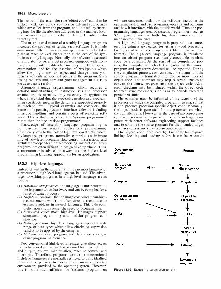
//integras/b&h/Eer/Final_06-09-02/eerc015
15/22 Microprocessors
The output of the assembler (the `object code') can then be `linked' with any library routines or external subroutines which are called from the program, and `located' by insert-ing into the file the absolute addresses of the memory loca-tions where the program code and data will loaded in the target system.
The unstructured nature of assembly-language programs increases the problem of testing such software. It is made even more difficult because testing conventionally takes place at machine level, rather than at the level of the sym-bolic assembly language. Normally, the software is executed on simulator, or on a target processor equipped with moni-tor program, with facilities for memory and CPU register examination, and for the insertion of breakpoints which allow the programmer to inspect and change memory or register contents at specified points in the program. Such testing requires skill, care and good management if it is to produce usable results.
Assembly-language programming, which requires a detailed understanding of instruction sets and processor architecture, is normally only necessary in applications where it is critical that the processing models and program-ming constructs used in the design are supported properly at machine level. Typical examples are compilers, the kernels of operating systems, interface software including interrupt handling, and certain aspects of real-time soft-ware. This is the province of the `systems programmer' rather than the `applications programmer'.
Knowledge of assembly language programming is not essential for general applications programming. Specifically, due to the lack of high-level constructs, assem-bly-language programs normally comprise an intimate mix of low-level program flow-control instructions and architecture-dependent data-processing instructions. Such programs are often difficult to design or comprehend. Thus, a programmer is advised to always use the highest level programming language appropriate for an application.
15.8.3 High-level languages
Instead of writing the programs in the assembly language of a processor, a high-level language can be used. The advan-tages to writing programs in a high-level language are as follows:
(1) Hardware independence: the language is independent of the implementation hardware and can be compiled for a range of target processor.
(2) High-level notation: the language comprises unambigu-ous statements which are often close to those used to express problems in natural language. This aids com-prehension and increases the speed of programming.
(3) Structured code: most high-level languages support structured programming and modular program con-struction.
(4) Data types: most high level languages support a wide range of data types which allow checks on expression validity to be applied by the compiler.
(5) Maintenance: clear program and data structures give easier program maintenance.
Few conventional high-level languages give direct access to machine-level primitives that are used for physical input and output, bit-level manipulation, machine control, and interrupts. Therefore, programs written in conventional high-level languages are normally restricted to using idealised input and output (e.g. to files) and are run in a protected environment provided by the operating system. However, this is not always sufficient for `systems' programmers
who are concerned with how the software, including the operating system and user programs, operates and performs and how it interfaces with the outside world. Thus, the pro-gramming languages used by systems programmers, such as `C', typically include both high-level constructs and machine-level primitives.
A high-level language program is prepared as a source text file using a text editor (or using a word processing facility capable of producing a text file in the required format). The high-level language program is translated into an object program (i.e. nearly executable machine code) by a compiler. At the start of the compilation pro-cess, the compiler will check the syntax of the source program and any errors detected will be reported. During the compilation process, each construct or statement in the source program is translated into one or more lines of object code. The compiler may require several passes to convert the source program into the object code. Also, error checking may be included within the object code to detect run-time errors, such as array bounds exceeding predefined limits.
The compiler must be informed of the identity of the processor on which the compiled program is to run, so that it can produce processor-specific object code. Normally, the object code is generated for the processor on which the compiler runs. However, in the case of microprocessor systems, it is common to prepare programs on larger com-puters with better software engineering support facilities and to compile the source program for the intended target processor (this is known as cross-compilation).
The object code produced by the compiler requires linking, locating and loading before it can be executed,
Figure 15.19 Stages in program development

//integras/b&h/Eer/Final_06-09-02/eerc015
Embedded systems 15/23
as shown in Figure 15.19. The linker resolves all external references in the object code, such as references to library subroutines or other program modules held as object files, and combines all these modules into a single executable program. It also locates the program by adjusting the addresses all data memory references (variables) and code location references (labels) to the values of locations at which the code and data will be loaded. (In the case of relocatable code and data, it simply calculates the correct base addresses.) Finally, the linked object modules are loaded into memory at a defined location by the loader ready for execution. (For ease of communication, the object program is often downline loaded into the target processor in HEX form, and converted into binary by the loader during the loading process.) When the program is loaded, it is resident in memory in the target machine ready for execution.
15.8.4 Real-time processes
Many engineering systems, such as embedded computer real-time systems, are required to maintain synchronism with an asynchronous external system, or to respond to stimuli from such a system, within a finite and specified delay. In real-time programming there is a primary need for a mechanism for handling the concept of time. Real-time sequential programming languages include an addi-tional primitive construct that allows the formal inclusion of time.
An application is said to be `time-critical' if it must per-form activities and produce responses at times dictated by an external environment. Typically in real-time control, a precise time-window is specified during which sensors must be sampled, a satisfactory control response computed, and output values sent to actuators. This schedule may re-occur periodically, or be initiated at irregular intervals by stimuli from the external system. Failure to perform the required functions in time is a fault; this may lead to system failure and may be hazardous.
The software for a time-critical application will comprise processes that must be properly synchronised with each other and with the external system. Synchronism with the external system is usually imposed by a `real-time clock' driven schedule; these times will not be dictated by the optimum use of computing resources. To ensure that com-ponent processes do not overrun, it is common to place (critical) timing requirements on software execution and to provide a `time-out' mechanism to warn of timing violations.
It is conventional to monitor the performance of a time-critical application process. Traditionally, this is done using a real-time time-lapse counter built as an external circuit. The counter is preset to trip after a pre-determined time and is initiated to run concurrently with the time-critical process. The first process to complete causes the other to abort. The mechanism is known as a `watch-dog' timer.
If the application process has been properly designed, it will produce results well before the maximum allowed time and the `watch-dog' timer will be aborted. The expiry of a `watch-dog' timer or `trip' indicates the presence of a fault (which may be a software design fault or a transient or permanent malfunction of the system) and appropriate fault recovery activities should be invoked. It is therefore necessary to set the pre-determined trip period to somewhat less than the time-critical time so that fault recovery can take place and the system can still provide a timely and satisfactory response.
15.8.5 Embedded real-time operating systems (RTOS)
A number of proprietary real-time operating systems (RTOS) are available for use in embedded microprocessor systems. These operating systems typically provide input/ output handling, deterministic real-time task scheduling, watchdog facilities, and default behaviour under fault conditions. They are also characterised by having modest memory requirements. Significantly, these operating systems are targeted at a range of processors including conventional microprocessors, commercial off-the-shelf (COTS) micro-computers, embedded controllers (microprocessors with built-in analogue and digital signal acquisition and output generation), and the more recently introduced system-on-chip (SoC) systems with on-chip embedded processors.
15.9 Embedded systems
Many products have computers, microprocessors, or micro-controllers hidden or embedded within them. Some devices, such as digital organisers or personal digital assistants (PDAs), resemble small computers and the user may be pro-vided with limited programming facilities for the embedded processor. In the case of other products, such as video games machines or consoles, it is fairly obvious that the device contains embedded processors and video display gen-erators, even though the user is given little or no facility for programming the device. A much wider range of products contains embedded processors that are hidden or invisible to the user. For example embedded processors are commonly found in the following: cellular or mobile telephones, automobile electronics (such as engine manage-ment, braking systems, active suspension, intelligent sensing for lights or windscreen wipers, navigation systems, and both in-car and in-seat entertainment systems), office auto-mation products (such as faxes, scanners, printers, copiers or duplicators, multimedia display projectors, computer network switches), domestic appliances (such as washing machines, dishwashers, tumble driers, cookers or ovens, microwave cookers, food blenders and processors, weigh scales, and vacuum cleaners), home entertainment units (such as radios, televisions, satellite receivers, digital set-top boxes, video cassette recorders, digital video disc (DVD) players, and hi-fi units), photographic equipment (such as film and digital cameras, analogue and digital video cameras) and personal or `wearable' electronics (such as portable radios and CD players, MP3 players, watches, and fitness monitors). The trend is to increase significantly the sophistication of such systems, including user adapta-tion or personalisation, and to increase very significantly the data handling and processing requirements of the embedded processor. This is leading to the development of extremely powerful processors that are designed specifi-cally for embedded applications, including small battery-powered products.
15.9.1 Embedded processors
The designer of embedded systems can choose from a wide range of processors. Classical microcontrollers, with integrated analogue inputs and outputs, are often used in control applications for domestic appliances or automotive systems. Specialist microcontrollers have been developed for applications such as electric motor control, or servo control. Traditional microprocessors or RISC processors may be used as stand alone devices within a more complex design.

//integras/b&h/Eer/Final_06-09-02/eerc015
15/24 Microprocessors
Increasingly, the trend is to minimise the number of com-ponents in an embedded system. Traditionally, conventional microprocessors tend to be poorly suited to integration within, say, an FPGA since they are relatively complex and are not scalable (i.e. smaller versions can not be readily generated), although these constraints may become less important as the size of FPGAs increase. RISC processors are much better suited to integration because they have powerful ALUs, small instruction sets and instruction decoders, and are scalable in terms of word-length, concurrent resource, instruction pipe-line, and clock speed. Embedded RISC processors are readily available as intellectual property (IP) cores.
Traditionally, IP cores have taken the form of hardware description language (HDL) software macros, which a designer incorporates within an application-specific design. However, the performance of such IP cores is layout depend-ent, and very careful design is necessary to achieve good speeds. Therefore, the preferred method of deriving high-performance designs is to use a proprietary `hard' IP core that provides guaranteed performance (i.e. an IP core that has been pre-mapped into a fixed and full-tested hardware layout on the intended FPGA target). The second advan-tage of using proprietary `hard' IP core RISC processors is that they are usually fully supported by proprietary embedded real-time operating system (RTOS) software and software tools for writing applications (such as editors and compilers). Thus the embedded systems design approach typically involves:
(1) Determining the application's processing requirements and selecting a proprietary `hard' IP RISC processor of appropriate performance, complexity, word length, and silicon area.
(2) Selecting a proprietary embedded RTOS that supports the processor.
(3) Developing application-specific software for software-implemented functions.
(4) Developing digital designs for any hardware-implemen-ted functions and interfaces.
Reconfigurable FPGA
15.9.2 System on chip (SoC) design
The increase in size of VLSI logic circuits has led to a new generation of reconfigurable FPGA devices that provide a platform for `hard' IP cores and are large enough to contain a complete high-performance digital processing system within a chip. These FPGAs are commonly called System on Chip (SoC) devices. An SoC device can be configured to include both `hard' and `soft' IP cores, plus user-designed digital circuits, Figure 15.20. At the heart of most SoC designs are an embedded proprietary RISC processor and a block of RAM memory (for the software that runs on the processor). This allows the designer to partition a design into those parts that will be implemented as software executing on the embedded processor (under an appropriate embedded RTOS) and those parts that will be implemented in hardware as high-speed application-specific logic circuits. This design approach, known as co-design or co-ware, has the significant advantage that established and high-perfor-mance parts of the design can be committed to application-specific hardware, and more adventurous parts of the design or low-speed functions can be committed to easily changed software.
The high-performance hardware implemented applica-tion-specific logic circuits may make extensive use of both `hard'- and `soft'- IP cores. In particular, SoC devices commonly provide co-processor support for digital signal processing, typically using a proprietary `hard' IP digital signal processor (DSP). Alternatively, specific algorithms may be implemented using either `hard'- or `soft'- IP digital signal processing circuits. Similarly, signal acquisition may be facilitated using mixed-signal (digital/analogue) com-ponents such as analogue-to-digital (A/D) or digital-to-analogue (D/A) convertors. The problem of interfacing such major components is eased by the on-chip provision of advanced data highways or buses, standardised bus interfaces (for the major components such as the RISC/ DSP processors and the memory), sophisticated clock generators, and a clock management unit.
System control, address and data bus with standardised interfaces
‘Hard’-IP RISC processor
‘Hard’-IP DSP management
and test subsystem
‘Soft’-IP digital circuits
‘Hard’-IP High-speed input/output
Memory Clock
Configuration Mixed-signal
Communication Analogue Configuration networks, input/output and test data peripherals and displays
Figure 15.20 Typical system-on-chip (SoC) configuration
//integras/b&h/Eer/Final_06-09-02/eerc015
Embedded systems 15/25
External interfacing is facilitated by the use of `hard' IP cores that support a wide range of high-bandwidth interface standards (for high-speed serial and parallel interfaces, including either system- or source-synchronous parallel interfaces). This is an area of on-going development, and both the SoC vendors and third-party IP providers are developing IP cores to support the ever widening range of communications protocols and interface standards found in the embedded systems market.
Modern SoC devices and the co-design approach, (invol-ving embedded RTOS software, `soft'- and `hard'-IP cores, and bespoke digital design), provides a manageable and flexible route to embedded systems design. It may also change the relative roles of the hardware and software
designer in the development of SoC designs. The reconfi-gurable SoC devices can be deployed in a wide range of applications and the common-platform nature of the devices helps avoid the non-recurring costs associated with fully bespoke designs. The extensive use of `hard'- and `soft'-IP from SoC vendors and third party suppliers mini-mises risk and facilitates time-to-market which gives com-petitive advantage. However, it also involves entering into IP license arrangements for both product development and deployment. It will be interesting to see whether the rapidly decreasing SoC product design cycles are complemented by corresponding decreases in the time, complexity, and cost of negotiating multi-party IP license agreements.

//integras/b&h/Eer/Final_06-09-02/eerc015