Embed Size (px)
Citation preview
16
Accurate LDMOS Model Extraction using DC, CV and Small Signal S Parameters
Measurements for Reliability Issues
Mouna Chetibi-Riah1, Mohamed Masmoudi1, Hichame Maanane 2, Jérôme Marcon1, Karine Mourgues1, Mohamed Ketata1 and Philippe Eudeline2
1University of Rouen 2THALES AIR SYSTEMS
France
1. Introduction
It is well recognized that excellent power performance and linearity can be achieved at low cost using Laterally Diffused Metal-Oxide-Semiconductor (LDMOS) field effect transistor. In fact, it is the preferred technology for base station applications as well as many other RF and microwave applications (Wood et al., 2006). But system’s availability and reliability are important parameters in terms of ownership cost for the customer. That’s the reason why a precise knowledge of the device’s degradation mechanisms and lifetime is of paramount importance. Thus modelling and reliability study of the LDMOS technologies are being increasingly used by the power amplifier design community. Numerous applications for power integrated circuits are emerging, which needs to operate at high temperatures. In the radar field, a crucial issue to tackle with is the reliability of RF LDMOS subjected to RF pulses with high drain-source DC bias for maximum output power under wide temperature range (Maanane et al., 2006). Those requirements raise the stress (thermal, electrical and RF power) applied to the transistors and have a direct impact on their lifetime. A deep understanding of this impact is necessary for better device and radar module reliability assessment. Moreover, a study has been engaged to elaborate new methods for RF power device reliability investigations under pulsed RADAR conditions (Maanane et al., 2004). In this chapter, we present an innovative reliability bench designed and implemented in our laboratory by (Maanane et al., 2004). It is specifically dedicated to high RF power device lifetime tests under pulse conditions for radar application and able to keep track of RF powers, voltages and temperatures whose values correspond to stress operating conditions. It clearly appears the need to track electrical parameters that lead to modifications of both the device RF performances and the critical electrical parameters with time (Poole & Walshak, 1974, Sirenza Microdevices, 2002). In this work, we will go step by step through the individual characterization issues and develop the model parameters extraction strategies which will provide the base for accurate device modelling. A commercial RF LDMOS transistor has been chosen for RF life-tests and a complete device electric characterization, I-V, C-V and S parameters, before and after test ageing has been
www.intechopen.com
Micro Electronic and Mechanical Systems
246
conducted. RF LDMOS modelling and parameters extraction are performed before and after life test in order to have a better insight on impact of the stress tests. With this intention, a refinement to the electro-thermal MET LDMOS model is presented, including the inductances in series as parasitic components in the extrinsic circuit. A methodology for the accurate extraction of model parameters is developed. The LDMOS model is compared to DC and small signal measurements. It is shown that the DC and RF performances of the device model closely match the measured data. The extracted non-linear model will be used as a reliability tool in order to correlate RF LDMOS electrical parameter drifts with any kind of degradation phenomenon, after different life-tests (DC and/or RF life-tests). Thus, a whole review of critical electrical parameters of the device is exposed and analysed. All the electrical parameters (POUT, IDSS, CRSS, RDSON, ft, fmax, Gmax, etc.) drifts after accelerated ageing tests have been shown and discussed. RF-figures of merit such as ft, fmax and power gain of RF LDMOS show significant vulnerability to the self heating and hot-carrier effects. This study clearly explains the physical degradation mechanism occurred during RF life-tests, by means of 2D ATLAS-SILVACO simulations. According to the measurement and simulation results analysis, an observation can be made. At low temperature, the drift of significant parameters is more important. Finally, we have clearly demonstrate that N-LDMOS degradation mechanism, therefore, is self-heating effect and hot carrier generated interface states (traps) and trapped electrons, which results in a build-up of negative charge at Si/SiO2 interface. Last but not least, more interface states (i.e. important build-up of negative charge) are created at low temperature due to a located maximum impact ionisation rate at the gate edge (drain side). This is the reason why the electrical degradations are so high at low temperature.
2. Innovative reliability bench
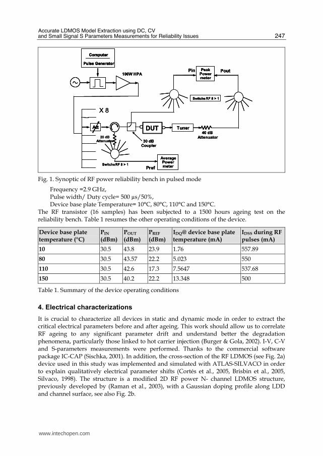
An innovative reliability bench designed to apply both electrical and thermal stress (Fig.1) has been implemented. The bench capacity has been limited to eight devices to be tested simultaneously for the simplicity of use. The bench is divided in three modules (Maanane et al., 2004):
• a microwave module,
• a control/command module driven by PC,
• one thermal module for each device (Peltier or high temperature module). Peltier and high temperature modules give us the capability to cool or heat each device independently for optimal temperature regulation and maximum flexibility.
3. Life-test conditions
Life-tests are run under RF conditions using different temperature settings and a high drain-source voltage in order to get more power from the device for radar applications. The applied drain voltage is 10% higher than the one applied on dedicated radar bipolar devices having same breakdown voltage (75 Vmin). In fact, the real RF LDMOS device breakdown voltage has been measured to be about 87 V. This justifies the applied drain-source voltage value (44 V). The discrete RF device is a commercial 10 W telecom dedicated transistor with a gate length equal to 0.8 µm and that operates in class-B at saturation. The parameters set for the tests are as following:
www.intechopen.com
Accurate LDMOS Model Extraction using DC, CV and Small Signal S Parameters Measurements for Reliability Issues
247
Computer
Pulse Generator
Pref
Pin
Tuner40 dB
Attenuator
DUT
Average Power meter
Peak Power meter
Pout
Att
X 8
SwitchsRF 8 > 1
20 dB Attenuator 30 dB
Coupler
SwitchsRF 8 > 1
100W HPA
Computer
Pulse Generator
Pref
Pin
Tuner40 dB
Attenuator
DUT
Average Power meter
Peak Power meter
Pout
Att
X 8
SwitchsRF 8 > 1
20 dB Attenuator 30 dB
Coupler
SwitchsRF 8 > 1
100W HPA
Computer
Pulse Generator
Computer
Pulse Generator
Pref
Pin
Tuner40 dB
Attenuator
DUT
Average Power meter
Peak Power meter
Pout
AttAtt
X 8
SwitchsRF 8 > 1
20 dB Attenuator 30 dB
Coupler
SwitchsRF 8 > 1
100W HPA
Fig. 1. Synoptic of RF power reliability bench in pulsed mode
Frequency =2.9 GHz, Pulse width/ Duty cycle= 500 µs/50%, Device base plate Temperature= 10°C, 80°C, 110°C and 150°C.
The RF transistor (16 samples) has been subjected to a 1500 hours ageing test on the reliability bench. Table 1 resumes the other operating conditions of the device.
Device base plate temperature (°C)
PIN (dBm)
POUT (dBm)
PREF (dBm)
IDQ@ device base plate temperature (mA)
IDSS during RF pulses (mA)
10 30.5 43.8 23.9 1.76 557.89
80 30.5 43.57 22.2 5.023 550
110 30.5 42.6 17.3 7.5647 537.68
150 30.5 40.2 22.2 13.348 500
Table 1. Summary of the device operating conditions
4. Electrical characterizations
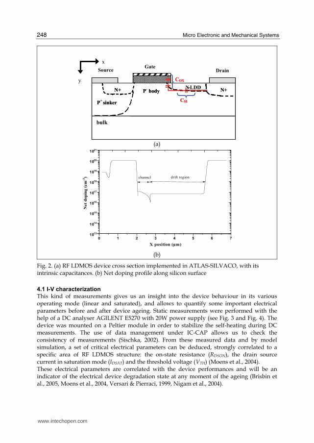
It is crucial to characterize all devices in static and dynamic mode in order to extract the critical electrical parameters before and after ageing. This work should allow us to correlate RF ageing to any significant parameter drift and understand better the degradation phenomena, particularly those linked to hot carrier injection (Burger & Gola, 2002). I-V, C-V and S-parameters measurements were performed. Thanks to the commercial software package IC-CAP (Sischka, 2001). In addition, the cross-section of the RF LDMOS (see Fig. 2a) device used in this study was implemented and simulated with ATLAS-SILVACO in order to explain qualitatively electrical parameter shifts (Cortés et al., 2005, Brisbin et al., 2005, Silvaco, 1998). The structure is a modified 2D RF power N- channel LDMOS structure, previously developed by (Raman et al., 2003), with a Gaussian doping profile along LDD and channel surface, see also Fig. 2b.
www.intechopen.com
Micro Electronic and Mechanical Systems
248
N+ N+
SourceGate
Drain
bulk
x
y
N-LDD
P+
sinker
P-
body
COX
CSI
N+ N+
SourceGate
Drain
bulk
x
y
N-LDD
P+
sinker
P-
body
COX
CSI
(a)
0 1 2 3 4 5 6 7
1013
1014
1015
1016
1017
1018
1019
1020
1021
X position (µm)
drift region
channel
Net
do
pin
g (
cm
-3)
(b)
Fig. 2. (a) RF LDMOS device cross section implemented in ATLAS-SILVACO, with its intrinsic capacitances. (b) Net doping profile along silicon surface
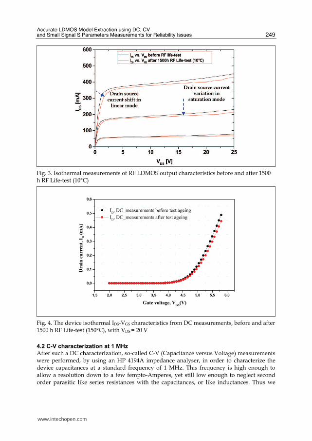
4.1 I-V characterization
This kind of measurements gives us an insight into the device behaviour in its various operating mode (linear and saturated), and allows to quantify some important electrical parameters before and after device ageing. Static measurements were performed with the help of a DC analyser AGILENT E5270 with 20W power supply (see Fig. 3 and Fig. 4). The device was mounted on a Peltier module in order to stabilize the self-heating during DC measurements. The use of data management under IC-CAP allows us to check the consistency of measurements (Sischka, 2002). From these measured data and by model simulation, a set of critical electrical parameters can be deduced, strongly correlated to a specific area of RF LDMOS structure: the on-state resistance (RDSON), the drain source current in saturation mode (IDSAT) and the threshold voltage (VTH) (Moens et al., 2004). These electrical parameters are correlated with the device performances and will be an indicator of the electrical device degradation state at any moment of the ageing (Brisbin et al., 2005, Moens et al., 2004, Versari & Pierraci, 1999, Nigam et al., 2004).
www.intechopen.com
Accurate LDMOS Model Extraction using DC, CV and Small Signal S Parameters Measurements for Reliability Issues
249
Fig. 3. Isothermal measurements of RF LDMOS output characteristics before and after 1500 h RF Life-test (10°C)
1,5 2,0 2,5 3,0 3,5 4,0 4,5 5,0 5,5 6,0
0,0
0,1
0,2
0,3
0,4
0,5
0,6
ID, DC_measurements before test ageing
ID, DC_measurements after test ageing
Dra
in c
urr
ent,
ID (
mA
)
Gate voltage, VGS
(V)
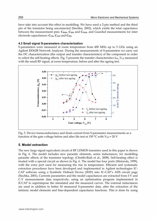
Fig. 4. The device isothermal IDS-VGS characteristics from DC measurements, before and after 1500 h RF Life-test (150°C), with VDS = 20 V
4.2 C-V characterization at 1 MHz
After such a DC characterization, so-called C-V (Capacitance versus Voltage) measurements were performed, by using an HP 4194A impedance analyser, in order to characterize the device capacitances at a standard frequency of 1 MHz. This frequency is high enough to allow a resolution down to a few fempto-Amperes, yet still low enough to neglect second order parasitic like series resistances with the capacitances, or like inductances. Thus we
www.intechopen.com
Micro Electronic and Mechanical Systems
250
have take into account this effect in modelling. We have used a 2-pin method and the third pin of the transistor being unconnected (Sischka, 2002), which yields the total capacitance between the measurement pins: CRSS, CISS and COSS, and Guarded measurements for inter electrode capacitances: CGS, CGD and CDS.
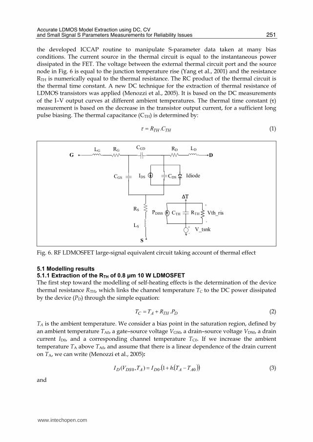
4.3 Small signal S-parameters characterization
S-parameters were measured at room temperature from 490 MHz up to 5 GHz using an Agilent E8362B Network Analyser. During the measurements of S-parameters we carry out the DC characterization (the output and transfer characteristics) of the component in order to solicit the self-heating effects. Fig. 5 presents the transfer characteristics IDS_VGS measured with the small RF signal, at room temperature, before and after the ageing test.
3 4 5 6 7 8
-0,02
-0,01
0,00
0,01
0,02
0,03
0,04
0,05
Gate voltage, VGS
[V]
Tra
nsc
on
du
ctan
ce, |g
m| [S
]
|gm| before test ageing
|gm| after test ageing
0
100
200
300
400
500
Dra
in cu
rrent, I
D (mA
)
ID before test ageing
ID after test ageing
Fig. 5. Device transconductance and drain current from S-parameter measurements as a function of the gate voltage before and after life test at 150 °C with VDS = 20 V
5. Model extraction
The new large signal equivalent circuit of RF LDMOS transistor used in this paper is shown in Fig. 6. The model includes new parasitic elements, series inductances, for modelling parasitic effects of the transistor topology (Chetibi-Riah et al., 2008). Self-heating effect is treated with a special circuit as shown in Fig. 6. The model has four ports (Motorola, 1999), with the extra port used for measuring the rise in temperature. Efficient and systematic extraction procedures have been developed and implemented in Agilent technologies IC-CAP software using a Symbolic Defined Device (SDD) into IC-CAP’s ADS circuit page (Sischka, 2001). Currents parameters and the model capacitances are extracted from I-V and C-V measurements data respectively, using an optimisation program implemented in ICCAP to superimpose the simulated and the measured curves. The external inductances are used in addition to better fit measured S-parameter data, after the extraction of the intrinsic model elements and bias-dependent capacitance functions. This is done by using
www.intechopen.com
Accurate LDMOS Model Extraction using DC, CV and Small Signal S Parameters Measurements for Reliability Issues
251
the developed ICCAP routine to manipulate S-parameter data taken at many bias conditions. The current source in the thermal circuit is equal to the instantaneous power dissipated in the FET. The voltage between the external thermal circuit port and the source node in Fig. 6 is equal to the junction temperature rise (Yang et al., 2001) and the resistance RTH is numerically equal to the thermal resistance. The RC product of the thermal circuit is the thermal time constant. A new DC technique for the extraction of thermal resistance of LDMOS transistors was applied (Menozzi et al., 2005). It is based on the DC measurements
of the I–V output curves at different ambient temperatures. The thermal time constant (τ) measurement is based on the decrease in the transistor output current, for a sufficient long pulse biasing. The thermal capacitance (CTH) is determined by:
THTH CR .=τ (1)
S
G
LD
LS
RS
CGS Idiode
RDCGD
D
CDS
RG LG
CTH PDISS
ΔΤ
+
-V_tsnk
+
-
Vth_ris
IDS
RTH
Fig. 6. RF LDMOSFET large-signal equivalent circuit taking account of thermal effect
5.1 Modelling results 5.1.1 Extraction of the RTH of 0.8 μm 10 W LDMOSFET
The first step toward the modelling of self-heating effects is the determination of the device
thermal resistance RTH, which links the channel temperature TC to the DC power dissipated
by the device (PD) through the simple equation:
DTHAC PRTT .+= (2)
TA is the ambient temperature. We consider a bias point in the saturation region, defined by
an ambient temperature TA0, a gate–source voltage VGS0, a drain–source voltage VDS0, a drain
current ID0, and a corresponding channel temperature TC0. If we increase the ambient
temperature TA above TA0, and assume that there is a linear dependence of the drain current
on TA, we can write (Menozzi et al., 2005):
( )( )000 .1.),( AADADSD TThITVI −+= (3)
and
www.intechopen.com

Micro Electronic and Mechanical Systems
252
( )
hIdT
TVdID
A
ADSD .,
00 = (4)
The parameter h can thus be extracted by plotting ID(VDS0, TA) as a function of TA, and taking
the slope of the linear regression line.
We also assume that in the same TA range, the drain current is a linear function of the
channel temperature TC and we write (Menozzi et al., 2005):
( ) ( )( )0'
00 .1., CCDCDSD TThITVI −+= (5)
( )0',.
11ADSDTH TVPR
hh−= (6)
Thus, a plot of 1/h versus PD(VDS, TA0) should yield a straight line, from the slope of which
we deduce RTH.
10 20 30 40 50
1,005
1,010
1,015
1,020
1,025
1,030
1,035
1,040
1,045
1,050
1,055
5V
6V
7V
8V
9V
10V
Dra
in c
urr
ent,
ID
S [
A]
Ambient Temperature, TA [°C]
Fig. 7. Drain current of the 0.8 μm, 10 W LDMOS transistor measured at VGS = 7 V as a function of the ambient temperature TA for different values of VDS (legend). Best fit interpolations (solid lines)
Fig. 7 shows the measured drain current (ID) as a function of the ambient temperature TA for
different values of drain–source voltage (VDS) at a gate–source voltage VGS = 7 V. The VDS
range used for RTH extraction varies from 5 to 10 V and the ambient temperature TA ranging
from TA0 = 10 to 50°C. Since, this method assumes the thermal resistance to be constant
across the range of TA and VDS values used in the extraction. Best fit interpolations (solid
lines) show that the linearity assumption of (2) holds good in the chosen temperature and
voltage ranges.
In Fig. 8, the reciprocals of the values of h show a linear dependence on PD(VDS, TA0) = VDS.
ID(VDS, TA0), TA0 = 10 °C, as predicted by (5). The absolute value of the slope of the linear
regression line is therefore the device thermal resistance RTH = 5.34 °C/W.
www.intechopen.com
Accurate LDMOS Model Extraction using DC, CV and Small Signal S Parameters Measurements for Reliability Issues
253
4 5 6 7 8 9 10 11
-1900
-1850
-1800
-1750
-1700
-1650
-1600
-1550
-1500
-1450
-1400
-1350
-1300
1/h= -8,24 PD-1357
1/h= -5,34 PD-1762
1/h before RF life test
1/h after RF life test
1/h
[d
egre
e C
elsi
us]
Dissipated Power,PD(V
DS,T
A0) [watt]
Fig. 8. Extraction of RTH of the 0.8 μm and 10 W LDMOS transistor before and after RF life test (the solid line is the linear best fit, the slope of which yields RTH)
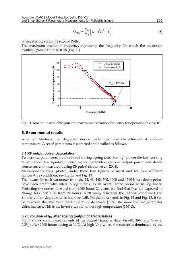
5.1.2 Extraction of current and capacitances parameters of the model The extraction of current and capacitance parameters of the model is performed from I-V and C-V measurements data respectively, using an optimization program implemented in ICCAP to fit simulations with measurements. Small-signal simulations are performed to validate the model for small signal operation (Chetibi-Riah et al., 2008). Fig. 9 shows good agreement between small-signal S-parameters simulations obtained from the new model (with/without inductances) and the small-signal measured data. The extracted parasitic inductances LG, LD and LS with the three dependent parasitic resistances RG, RD and RS are presented in the Table 2.
Fig. 9. Measured and modelled S-parameters before and after refinements with frequency = [0.5, 5] GHz and operating at class B
www.intechopen.com

Micro Electronic and Mechanical Systems
254
Parameter Value Unit
LG 1.459 nH
LD 970 pH
LS 75 pH
RG 795 mΩ
RD 700 mΩ
RS 100 mΩ
Table 2. Extracted parasitic elements
5.2 The new main significant RF LDMOS figures of merit
The threshold voltage, the breakdown voltage, the saturation current… are the classical
parameters used as indicator in a reliability study. Thanks to the modelling approach, we
can also extract other relevant parameters such as the power gain, the cut-off frequency (ft),
the maximum oscillation frequency (fMax), … which can be used to study the device
reliability.
5.2.1 Current gain and cut-off frequency
The current gain is defined from the S-parameters as:
21122211
2121
.)1)(1(
.2
SSSS
SH ++−
−= (7)
The cut-off frequency represents the frequency for which the current gain is equal to 1 (Fig. 10).
1 10
0,1
1
10
FT = 2,3 GHz
|H21| measured
|H21| modelled
Cu
rren
t gain
, |H
21|
Frequency [GHz]
Fig. 10. Current gain and cut-off frequency for operation in class B
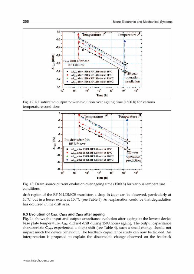
5.2.2 Maximum available gain and maximum oscillation frequency
The expression of the maximum available gain from the transistor S-parameters is given by:
www.intechopen.com
Accurate LDMOS Model Extraction using DC, CV and Small Signal S Parameters Measurements for Reliability Issues
255
⎟⎠⎞⎜⎝
⎛ −−= 12
12
21 KKS
SGMax (8)
where K is the stability factor of Rollet. The maximum oscillation frequency represents the frequency for which the maximum available gain is equal to 0 dB (Fig. 11).
1 10
-5
0
5
10
15
20
25
Fmax
= 4,7 GHz
Gmax measured
Gmax modelled
Maxim
um
avail
ab
le g
ain
, G
max[d
B]
Frequency [GHz]
Fig. 11. Maximum available gain and maximum oscillation frequency for operation in class B
6. Experimental results
After RF life-tests, the degraded device under test was characterized at ambient
temperature. A set of parameters is extracted and detailed as follows.
6.1 RF output power degradation
Two critical parameters are monitored during ageing tests. For high power devices working
at saturation, the significant performance parameters concern output power and drain-
source current (measured during RF pulse) (Brown et al., 2004).
Measurements were plotted under these two figures of merit and for four different temperature conditions, see Fig. 12 and Fig. 13. The means for each parameter from the 24, 48, 168, 500, 1000 and 1500 h test down-points
have been empirically fitted to log curves, as an overall trend seems to be log linear.
Projecting the curves forward from 1500 hours 20 years, we find that IDSS are expected to
change less than 10% from 24 hours to 20 years, whatever the thermal conditions are.
Similarly, PSAT degradation is less than 1dB. On the other hand, in Fig. 12 and Fig. 13, it can
be observed that the more the temperature decreases (10°C) the more the two parameter
drifts increase. This is the invert situation under high temperature (150°C).
6.2 Evolution of IDS after ageing (output characteristics)
Fig. 3 shows static measurements of the output characteristics (VDS=[0, 26V] and VGS=[2, 5.8V]) after 1500 hours ageing at 10°C. At high VGS, where the current is dominated by the
www.intechopen.com
Micro Electronic and Mechanical Systems
256
Fig. 12. RF saturated output power evolution over ageing time (1500 h) for various temperature conditions
Fig. 13. Drain source current evolution over ageing time (1500 h) for various temperature conditions
drift region of the RF N-LDMOS transistor, a drop in IDSAT can be observed, particularly at
10°C, but in a lesser extent at 150°C (see Table 3). An explanation could be that degradation
has occurred in the drift area.
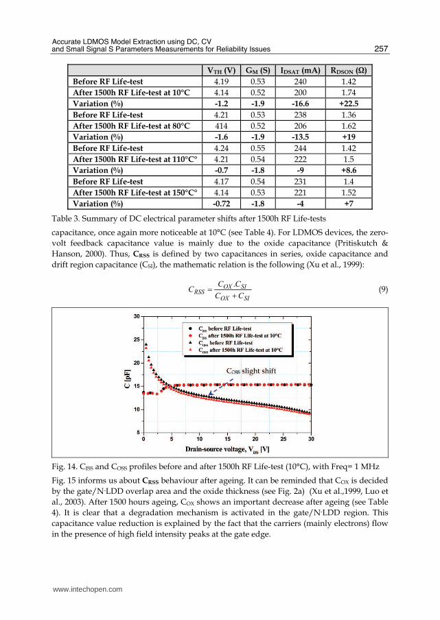
6.3 Evolution of CISS, COSS and CRSS after ageing
Fig. 14 shows the input and output capacitance evolution after ageing at the lowest device base plate temperature. CISS did not drift during 1500 hours ageing. The output capacitance characteristic COSS experienced a slight shift (see Table 4), such a small change should not impact much the device behaviour. The feedback capacitance study can now be tackled. An interpretation is proposed to explain the discernable change observed on the feedback
www.intechopen.com
Accurate LDMOS Model Extraction using DC, CV and Small Signal S Parameters Measurements for Reliability Issues
257
VTH (V) GM (S) IDSAT (mA) RDSON (Ω)
Before RF Life-test 4.19 0.53 240 1.42
After 1500h RF Life-test at 10°C 4.14 0.52 200 1.74
Variation (%) -1.2 -1.9 -16.6 +22.5
Before RF Life-test 4.21 0.53 238 1.36
After 1500h RF Life-test at 80°C 414 0.52 206 1.62
Variation (%) -1.6 -1.9 -13.5 +19
Before RF Life-test 4.24 0.55 244 1.42
After 1500h RF Life-test at 110°C° 4.21 0.54 222 1.5
Variation (%) -0.7 -1.8 -9 +8.6
Before RF Life-test 4.17 0.54 231 1.4
After 1500h RF Life-test at 150°C° 4.14 0.53 221 1.52
Variation (%) -0.72 -1.8 -4 +7
Table 3. Summary of DC electrical parameter shifts after 1500h RF Life-tests
capacitance, once again more noticeable at 10°C (see Table 4). For LDMOS devices, the zero-
volt feedback capacitance value is mainly due to the oxide capacitance (Pritiskutch &
Hanson, 2000). Thus, CRSS is defined by two capacitances in series, oxide capacitance and
drift region capacitance (CSI), the mathematic relation is the following (Xu et al., 1999):
SIOX
SIOXRSS
CC
CCC += .
(9)
Fig. 14. CISS and COSS profiles before and after 1500h RF Life-test (10°C), with Freq= 1 MHz
Fig. 15 informs us about CRSS behaviour after ageing. It can be reminded that COX is decided
by the gate/N-LDD overlap area and the oxide thickness (see Fig. 2a) (Xu et al.,1999, Luo et
al., 2003). After 1500 hours ageing, COX shows an important decrease after ageing (see Table
4). It is clear that a degradation mechanism is activated in the gate/N-LDD region. This
capacitance value reduction is explained by the fact that the carriers (mainly electrons) flow
in the presence of high field intensity peaks at the gate edge.
www.intechopen.com
Micro Electronic and Mechanical Systems
258
CISS (pF) at 26
V@ 25°C COSS (pF) at 26
V@ 25°C CRSS (pF) at 0
V@ 25°C CRSS (pF) at 26
V@ 25°C
Before RF Life-test 15,3 10,25 2,58 0,43
After 1500h RF Life-test at 10°C
15,36 9,77 1,82 0,34
Variation (%) +0,4 -4,7 -29,5 -21
Before RF Life-test 15,3 10,1 2,52 0,46
After 1500h RF Life-test at 80°C
15,3 9,79 1,8 0,35
Variation (%) +0 -3 -28,6 -23,9
Before RF Life-test 14,9 10,2 2,12 0,34
After 1500h RF Life-test at 110°C
14,9 9,9 1,68 0,27
Variation (%) +0 -3 -20,75 -20,58
Before RF Life-test 15,3 10,1 2,52 0,44
After 1500h RF Life-test at 150°C
15,4 9,9 2,1 0,37
Variation (%) +0,65 -3 -16,6 -15,9
Table 4. Summary of CV electrical parameter shifts after 1500h RF Life-tests
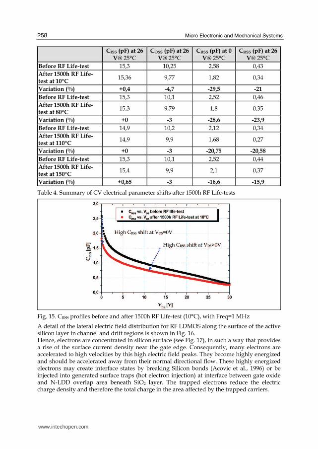
Fig. 15. CRSS profiles before and after 1500h RF Life-test (10°C), with Freq=1 MHz
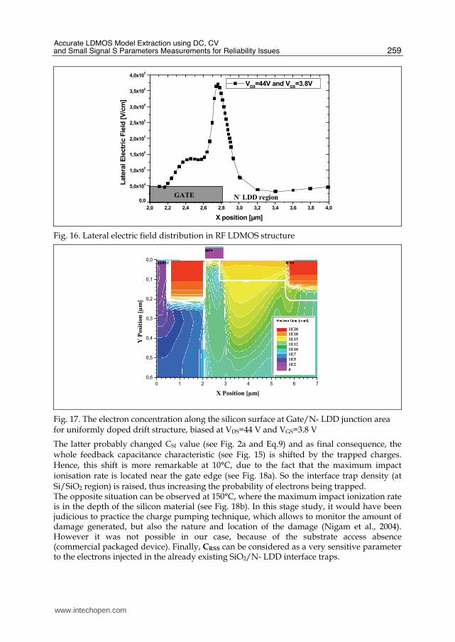
A detail of the lateral electric field distribution for RF LDMOS along the surface of the active silicon layer in channel and drift regions is shown in Fig. 16. Hence, electrons are concentrated in silicon surface (see Fig. 17), in such a way that provides a rise of the surface current density near the gate edge. Consequently, many electrons are accelerated to high velocities by this high electric field peaks. They become highly energized and should be accelerated away from their normal directional flow. These highly energized electrons may create interface states by breaking Silicon bonds (Acovic et al., 1996) or be injected into generated surface traps (hot electron injection) at interface between gate oxide and N-LDD overlap area beneath SiO2 layer. The trapped electrons reduce the electric charge density and therefore the total charge in the area affected by the trapped carriers.
www.intechopen.com
Accurate LDMOS Model Extraction using DC, CV and Small Signal S Parameters Measurements for Reliability Issues
259
GATE N- LDD region
2,0 2,2 2,4 2,6 2,8 3,0 3,2 3,4 3,6 3,8 4,0
0,0
5,0x10⁴
1,0x10⁵
1,5x10⁵
2,0x10⁵
2,5x10⁵
3,0x10⁵
3,5x10⁵
4,0x10⁵
VDS
=44V and VGS
=3.8V
Late
ral E
lectr
ic F
ield
[V
/cm
]
X position [µm]
Fig. 16. Lateral electric field distribution in RF LDMOS structure
0 1 2 3 4 5 6 7
0,6
0,5
0,4
0,3
0,2
0,1
0,0
X Position [µm]
Y P
osi
tion
[µ
m]
1E20
1E18
1E15
1E12
1E101E7
1E5
1E2
0
Fig. 17. The electron concentration along the silicon surface at Gate/N- LDD junction area for uniformly doped drift structure, biased at VDS=44 V and VGS=3.8 V
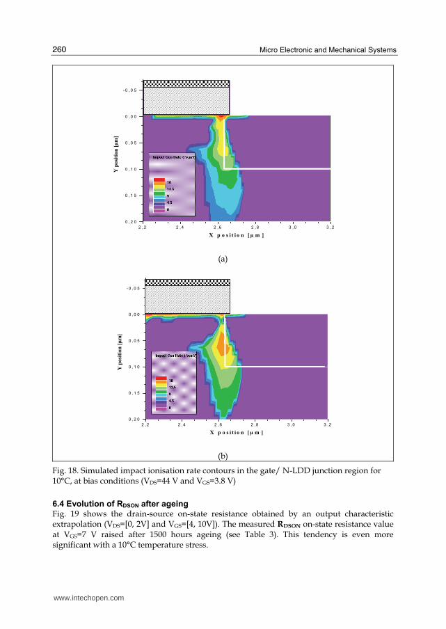
The latter probably changed CSI value (see Fig. 2a and Eq.9) and as final consequence, the whole feedback capacitance characteristic (see Fig. 15) is shifted by the trapped charges. Hence, this shift is more remarkable at 10°C, due to the fact that the maximum impact ionisation rate is located near the gate edge (see Fig. 18a). So the interface trap density (at Si/SiO2 region) is raised, thus increasing the probability of electrons being trapped. The opposite situation can be observed at 150°C, where the maximum impact ionization rate is in the depth of the silicon material (see Fig. 18b). In this stage study, it would have been judicious to practice the charge pumping technique, which allows to monitor the amount of damage generated, but also the nature and location of the damage (Nigam et al., 2004). However it was not possible in our case, because of the substrate access absence (commercial packaged device). Finally, CRSS can be considered as a very sensitive parameter to the electrons injected in the already existing SiO2/N- LDD interface traps.
www.intechopen.com
Micro Electronic and Mechanical Systems
260
2 , 2 2 , 4 2 , 6 2 , 8 3 , 0 3 , 2
0 , 2 0
0 , 1 5
0 , 1 0
0 , 0 5
0 , 0 0
- 0 , 0 5
X p o s i t i o n [ µ m ]
Y p
osi
tion
[µ
m]
(a)
2 ,2 2 ,4 2 ,6 2 ,8 3 ,0 3 ,2
0 ,2 0
0 ,1 5
0 ,1 0
0 ,0 5
0 ,0 0
- 0 ,0 5
X p o s i t io n [ µ m ]
Y p
osi
tion
[µ
m]
(b)
Fig. 18. Simulated impact ionisation rate contours in the gate/ N-LDD junction region for 10°C, at bias conditions (VDS=44 V and VGS=3.8 V)
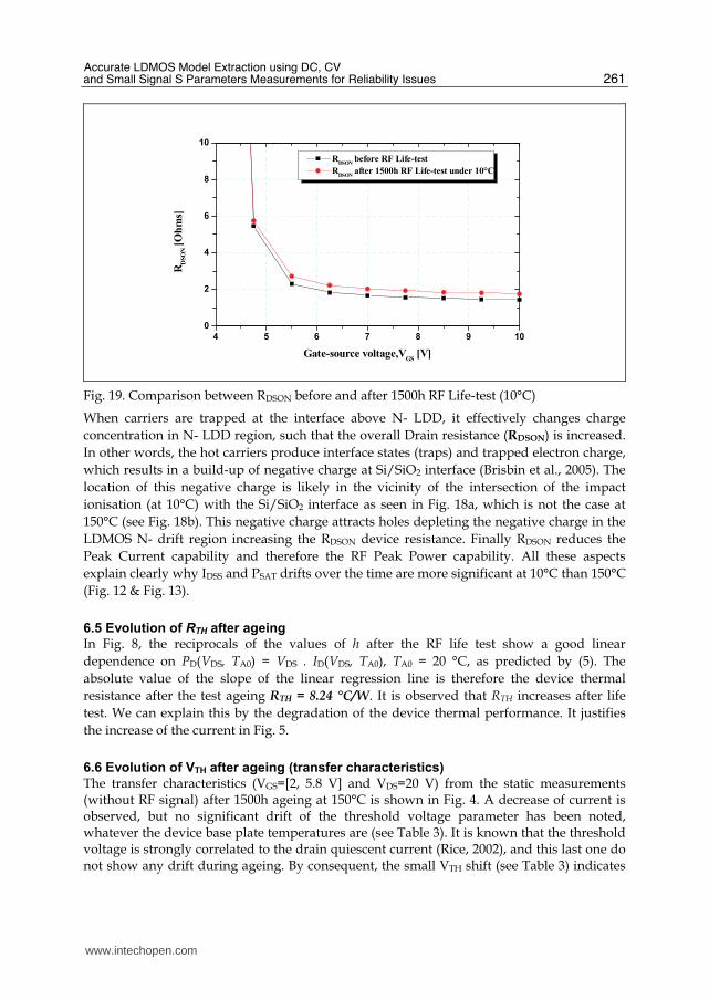
6.4 Evolution of RDSON after ageing
Fig. 19 shows the drain-source on-state resistance obtained by an output characteristic extrapolation (VDS=[0, 2V] and VGS=[4, 10V]). The measured RDSON on-state resistance value at VGS=7 V raised after 1500 hours ageing (see Table 3). This tendency is even more significant with a 10°C temperature stress.
www.intechopen.com
Accurate LDMOS Model Extraction using DC, CV and Small Signal S Parameters Measurements for Reliability Issues
261
4 5 6 7 8 9 10
0
2
4
6
8
10
RDSON
before RF Life-test
RDSON
after 1500h RF Life-test under 10°CR
DS
ON [
Oh
ms]
Gate-source voltage,VGS
[V]
Fig. 19. Comparison between RDSON before and after 1500h RF Life-test (10°C)
When carriers are trapped at the interface above N- LDD, it effectively changes charge
concentration in N- LDD region, such that the overall Drain resistance (RDSON) is increased.
In other words, the hot carriers produce interface states (traps) and trapped electron charge,
which results in a build-up of negative charge at Si/SiO2 interface (Brisbin et al., 2005). The
location of this negative charge is likely in the vicinity of the intersection of the impact
ionisation (at 10°C) with the Si/SiO2 interface as seen in Fig. 18a, which is not the case at
150°C (see Fig. 18b). This negative charge attracts holes depleting the negative charge in the
LDMOS N- drift region increasing the RDSON device resistance. Finally RDSON reduces the
Peak Current capability and therefore the RF Peak Power capability. All these aspects
explain clearly why IDSS and PSAT drifts over the time are more significant at 10°C than 150°C
(Fig. 12 & Fig. 13).
6.5 Evolution of RTH after ageing
In Fig. 8, the reciprocals of the values of h after the RF life test show a good linear
dependence on PD(VDS, TA0) = VDS . ID(VDS, TA0), TA0 = 20 °C, as predicted by (5). The
absolute value of the slope of the linear regression line is therefore the device thermal
resistance after the test ageing RTH = 8.24 °C/W. It is observed that RTH increases after life
test. We can explain this by the degradation of the device thermal performance. It justifies
the increase of the current in Fig. 5.
6.6 Evolution of VTH after ageing (transfer characteristics)
The transfer characteristics (VGS=[2, 5.8 V] and VDS=20 V) from the static measurements (without RF signal) after 1500h ageing at 150°C is shown in Fig. 4. A decrease of current is observed, but no significant drift of the threshold voltage parameter has been noted, whatever the device base plate temperatures are (see Table 3). It is known that the threshold voltage is strongly correlated to the drain quiescent current (Rice, 2002), and this last one do not show any drift during ageing. By consequent, the small VTH shift (see Table 3) indicates
www.intechopen.com
Micro Electronic and Mechanical Systems
262
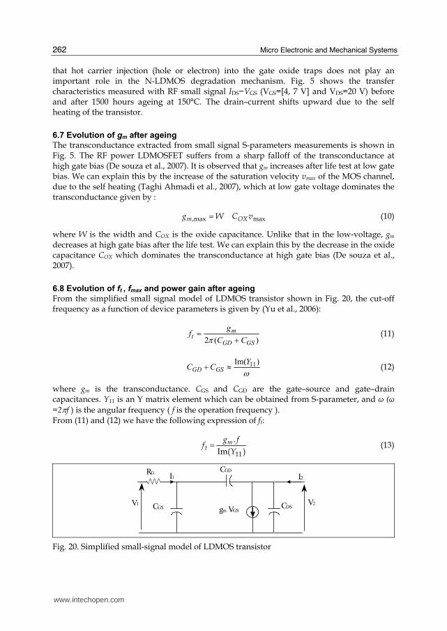
that hot carrier injection (hole or electron) into the gate oxide traps does not play an important role in the N-LDMOS degradation mechanism. Fig. 5 shows the transfer characteristics measured with RF small signal IDS−VGS (VGS=[4, 7 V] and VDS=20 V) before and after 1500 hours ageing at 150°C. The drain–current shifts upward due to the self heating of the transistor.
6.7 Evolution of gm after ageing
The transconductance extracted from small signal S-parameters measurements is shown in Fig. 5. The RF power LDMOSFET suffers from a sharp falloff of the transconductance at high gate bias (De souza et al., 2007). It is observed that gm increases after life test at low gate bias. We can explain this by the increase of the saturation velocity vmax of the MOS channel, due to the self heating (Taghi Ahmadi et al., 2007), which at low gate voltage dominates the transconductance given by :
maxmax, vCWg OXm = (10)
where W is the width and COX is the oxide capacitance. Unlike that in the low-voltage, gm decreases at high gate bias after the life test. We can explain this by the decrease in the oxide capacitance COX which dominates the transconductance at high gate bias (De souza et al., 2007).
6.8 Evolution of ft , fmax and power gain after ageing
From the simplified small signal model of LDMOS transistor shown in Fig. 20, the cut-off frequency as a function of device parameters is given by (Yu et al., 2006):
)(2 GSGD
mt
CC
gf += π (11)
ω)Im( 11YCC GSGD ≈+ (12)
where gm is the transconductance. CGS and CGD are the gate–source and gate–drain capacitances. Y11 is an Y matrix element which can be obtained from S-parameter, and ω (ω
=2πf ) is the angular frequency ( f is the operation frequency ). From (11) and (12) we have the following expression of ft:
)Im(
.
11Y
fgf mt = (13)
V2
CGD
CGS CDS gm VGS V1
I1 I2 RG
Fig. 20. Simplified small-signal model of LDMOS transistor
www.intechopen.com
Accurate LDMOS Model Extraction using DC, CV and Small Signal S Parameters Measurements for Reliability Issues
263
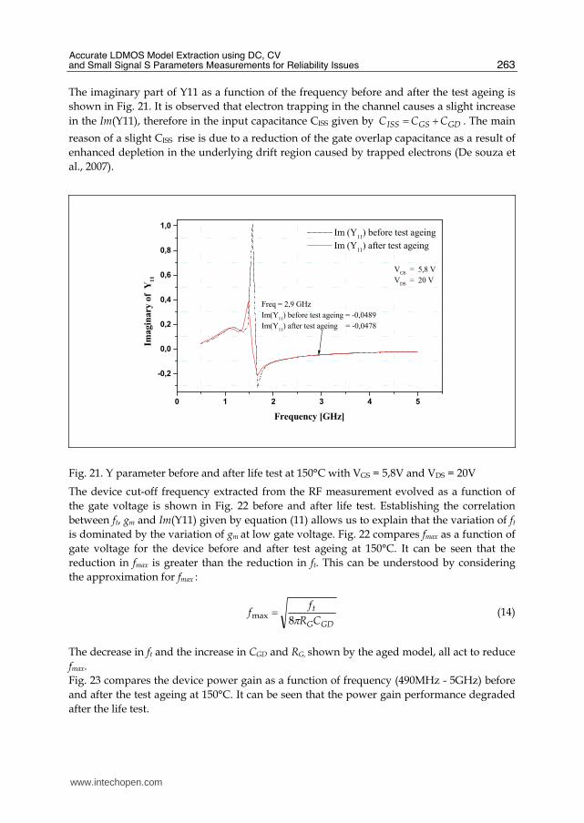
The imaginary part of Y11 as a function of the frequency before and after the test ageing is
shown in Fig. 21. It is observed that electron trapping in the channel causes a slight increase
in the Im(Y11), therefore in the input capacitance CISS given by GDGSISS CCC += . The main
reason of a slight CISS rise is due to a reduction of the gate overlap capacitance as a result of
enhanced depletion in the underlying drift region caused by trapped electrons (De souza et
al., 2007).
0 1 2 3 4 5
-0,2
0,0
0,2
0,4
0,6
0,8
1,0
Freq = 2,9 GHz
Im(Y11
) before test ageing = -0,0489
Im(Y11
) after test ageing = -0,0478
VGS
= 5,8 V
VDS
= 20 V
Im (Y11
) before test ageing
Im (Y11
) after test ageing
Imagin
ary
of
Y11
Frequency [GHz]
Fig. 21. Y parameter before and after life test at 150°C with VGS = 5,8V and VDS = 20V
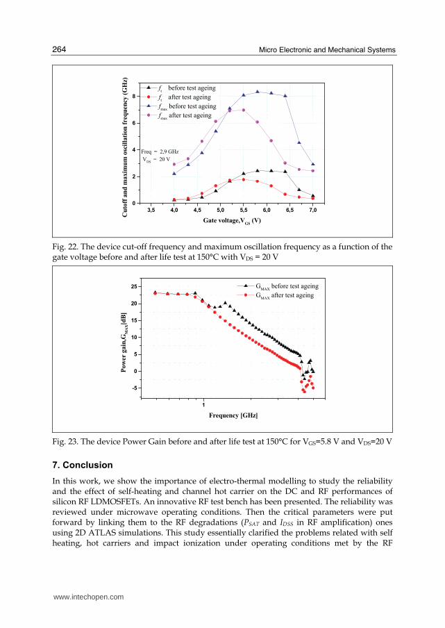
The device cut-off frequency extracted from the RF measurement evolved as a function of
the gate voltage is shown in Fig. 22 before and after life test. Establishing the correlation
between ft, gm and Im(Y11) given by equation (11) allows us to explain that the variation of ft
is dominated by the variation of gm at low gate voltage. Fig. 22 compares fmax as a function of
gate voltage for the device before and after test ageing at 150°C. It can be seen that the
reduction in fmax is greater than the reduction in ft. This can be understood by considering
the approximation for fmax :
GDG
t
CR
ff π8max = (14)
The decrease in ft and the increase in CGD and RG, shown by the aged model, all act to reduce
fmax.
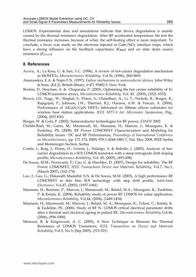
Fig. 23 compares the device power gain as a function of frequency (490MHz - 5GHz) before
and after the test ageing at 150°C. It can be seen that the power gain performance degraded
after the life test.
www.intechopen.com
Micro Electronic and Mechanical Systems
264
3,5 4,0 4,5 5,0 5,5 6,0 6,5 7,0
0
2
4
6
8
Freq = 2,9 GHz
VDS
= 20 V
ft before test ageing
ft after test ageing
fmax
before test ageing
fmax
after test ageing
Cu
toff
an
d m
axim
um
osc
illa
tion
fre
qu
ency
(G
Hz)
Gate voltage,VGS
(V)
Fig. 22. The device cut-off frequency and maximum oscillation frequency as a function of the gate voltage before and after life test at 150°C with VDS = 20 V
1
-5
0
5
10
15
20
25 GMAX
before test ageing
GMAX
after test ageing
Pow
er g
ain
,GM
AX[d
B]
Frequency [GHz]
Fig. 23. The device Power Gain before and after life test at 150°C for VGS=5.8 V and VDS=20 V
7. Conclusion
In this work, we show the importance of electro-thermal modelling to study the reliability and the effect of self-heating and channel hot carrier on the DC and RF performances of silicon RF LDMOSFETs. An innovative RF test bench has been presented. The reliability was reviewed under microwave operating conditions. Then the critical parameters were put forward by linking them to the RF degradations (PSAT and IDSS in RF amplification) ones using 2D ATLAS simulations. This study essentially clarified the problems related with self heating, hot carriers and impact ionization under operating conditions met by the RF
www.intechopen.com
Accurate LDMOS Model Extraction using DC, CV and Small Signal S Parameters Measurements for Reliability Issues
265
LDMOS. Experimental data and simulations indicate that device degradation is mainly caused by the thermal resistance degradation. After RF accelerated temperature life test the thermal resistance increases, because of what, the self-heating effect is more important. To conclude, a focus was made on the electrons injected in Gate/SiO2 interface traps, which have a strong influence on the feedback capacitance (CRSS) and on state drain source resistance (RDSON).
8. References
Acovic, A.; La Rosa, G. & Sun, Y.C. (1996), A review of hot-carrier degradation mechanism in MOSFETs, Microelectronics Reliability, Vol.36, (1996), (845-869)
Amerasekra, E.A. & Najm F.N. (1997), Failure mechanisms in semiconductor devices, John Wiley & Sons, (Ed.2), British library, 0 471 95482 9, New York
Brisbin, D.; Strachan, A. & Chaparala, P. (2005), Optimizing the hot carrier reliability of N-LDMOS transistor arrays, Microelectronics Reliability, Vol. 45, (2005), (1021-1032)
Brown, J.D.; Nagy, W.; Singhal, S.; Peters, S.; Chaudhari, A.; Li, T.; Nichols, R.; Borges, R.; Rajagopal, P.; Johnson, J.W.; Therrien, R.J.; Hanson, A.W. & Vescan, A. (2004), Performance of AlGaN/GaN HFETs fabricated on 100mm silicon substrates for wireless base station applications, IEEE MTT-S Int. Microwave Symposium, Dig., (2004), (833-836)
Burger, W. & Gola, P. (2002), Semiconductor technologies for RF power, ESNDF 2002 Chetibi-Riah, M.; Gares, M.; Masmoudi, M.; Maanane, H.; Marcon, J.; Mourgues, K. &
Eudeline, Ph. (2008), RF Power LDMOSFET Characterzation and Modeling for Reliability Issues : DC and RF Performances, Proceedings of International Conference on Microelectronics, pp. 171-174, ISBN 978-1-4244-1881-7, Niš, May 2008, IEEE Serbia and Montenegro Section, Serbia
Cortés, I.; Roig, J.; Flores, D.; Urresti, J.; Hidalgo, S. & Rebollo, J. (2005), Analysis of hot-carrier degradation in a SOI LDMOS transistor with a steep retrograde drift doping profile, Microelectronics Reliability, Vol. 45, (2005), (493-498)
De Souza, M.M.; Fioravanti, P.; Cao, G. & Hinchley, D. (2007), Design for reliability: The RF Power LDMOSFET, IEEE Transactions Device and Materials Reliability, Vol.7, No.1, (March 2007), (162-174)
Luo, J.; Gao, G.; Ekkanath Madathil, S.N. & De Souza, M.M. (2003), A high performance RF LDMOSFET in thin film SOI technology with step drift profile, Solid-State Electronics, Vol.47, (2003), (1937-1941)
Maanane, H.; Bertram, P.; Marcon, J.; Masmoudi, M.; Belaid, M.A.; Mourgues, K.; Eudeline, P. & Ketata, K. (2004). Reliability study of power RF LDMOS for radar application, Microelectronics Reliability, Vol.44, (2004), (1449-1454)
Maanane, H.; Masmoudi, M.; Marcon, J.; Belaid, M. A.; Mourgues, K.; Tolant, C.; Ketata, K. & Eudeline, Ph. (2006). Study of RF N- LDMOS critical electrical parameter drifts after a thermal and electrical ageing in pulsed RF, Microelectronics Reliability,Vol.46, (2006), (994-1000)
Menozzi, R. & Kingswood, A. C. (2005), A New Technique to Measure the Thermal Resistance of LDMOS Transistors, IEEE Transactions on Device and Materials Reliability, Vol.5, No.3, (Sep 2005), (515-521)
www.intechopen.com
Micro Electronic and Mechanical Systems
266
Motorola (1999), Motorola’s Electro Thermal (MET) LDMOS Model, on line: http://www.freescale.com/files/abstract/ldmos_models/MET_MODEL_DOCUMENT_0704.pdf
Moens, P.; Van den bosch, G.; De Keukeleire, C.; Degraeve, R.; Tack, M. & Groeseneken, G. (2004), Hot Hole Degradation Effects in Lateral nDMOS Transistors, IEEE Trans Electron Devices, Vol.51, No.10, (Oct. 2004), (1704-1710)
Nigam, T.; Shibib, A.; Xu, S.; Safar, H. & Steinberg, L. (2004) Nature and location of interface traps in RF LDMOS due to hot carriers, Microelectronic Engineering, Vol.72, (2004), (71-75)
Poole, W.E. & Walshak, L.G. (1974). Median-time-failure (MTF) of an L-band power transistor under RF conditions. Reliability physics, Proceedings of the Twelfth International Symposium, pp. 109-117, A75-13601 03-33, Las Vegas, April 1974, New York
Pritiskutch, J. & Hanson, B. (2000), Relate LDMOS device parameters to RF performance, St Microelectronics, Application note: AN 1228
Raman, A.; Walker, D. G. & Fisher, T. S. (2003), Simulation of nonequilibrium thermal effects in power LDMOS transistors, Solid-State Electronics, Vol.47, (2003), (1265-1273)
Rice, J. (2002), LDMOS linearity and reliability. (Technical Feature).(laterally diffused metal-oxide-semiconductors), Microwave Journal, (Jun 2002)
Silvaco International, (1998), Atlas User’s Manual-Device Simulation Software, Santa Clara, California
Sirenza Microdevices, (2002). Bias drift in LDMOS power FETs-A primer, Application Note: AN049, 2002
Sischka, F. (2001), IC-CAP user’s Guide 2001. Agilent technologies, Sischka, F. (2002), Characterization and modelling handbook, Munich Taghi Ahmadi, M.; Saad, I. ; L.P.Tan, M. ; Razali, I. & Vijay, K.A. (2007), The Ultimate Drift
Velocity in Degenerately-Doped Silicon, RSM 2007 Proc. 2007, Penang, Malaysia Versari, R. & Pierraci, A. (1999), Experimental study of hot-carrier effects in LDMOS
transistors, IEEE Transactions on Electron Devices, Vol. 46, No.6, (Jun 1999), (1228-1233)
Wood, A.; Brakensiek, W.; Dragon, C.; & Bruger, W. (1998). 120 watt, 2 GHz Si LDMOS RF power transistor for PCS base station applications, IEEE MTT-S Int. Microwave Symp. Dig., (1998), (707–710).
Xu, S.; Foo, P.; Wen, J.; Liu, Y.; Lin, F. & Ren, C. (1999) RF LDMOS with extreme low parasitic feedback capacitance and highhot-carrier immunity, Electron Devices Meeting, 1999 IEDM Technical Digest. International, (1999), (201-204)
Yang, Y.; Yi, J.; & Kim, B. (2001), Accurate RF Large-Signal Model of LDMOSFETs Including Self-Heating Effect, IEEE Transactions Microwave Theory and Techniques., Vol.49, (Feb 2001), (387-390)
Yu, C.; Yuan, J. S. & Suehle, J. (2006), Channel Hot-Electron Degradation on 60-nmHfO2 –Gated NMOSFET DC and RF Performances, IEEE Transactions on Electron devices, Vol. 53, No. 5, (May 2006), (1065-1072)
www.intechopen.com
Micro Electronic and Mechanical SystemsEdited by Kenichi Takahata
ISBN 978-953-307-027-8Hard cover, 386 pagesPublisher InTechPublished online 01, December, 2009Published in print edition December, 2009
InTech EuropeUniversity Campus STeP Ri Slavka Krautzeka 83/A 51000 Rijeka, Croatia Phone: +385 (51) 770 447 Fax: +385 (51) 686 166www.intechopen.com
InTech ChinaUnit 405, Office Block, Hotel Equatorial Shanghai No.65, Yan An Road (West), Shanghai, 200040, China
Phone: +86-21-62489820 Fax: +86-21-62489821
This book discusses key aspects of MEMS technology areas, organized in twenty-seven chapters that presentthe latest research developments in micro electronic and mechanical systems. The book addresses a widerange of fundamental and practical issues related to MEMS, advanced metal-oxide-semiconductor (MOS) andcomplementary MOS (CMOS) devices, SoC technology, integrated circuit testing and verification, and otherimportant topics in the field. Several chapters cover state-of-the-art microfabrication techniques and materialsas enabling technologies for the microsystems. Reliability issues concerning both electronic and mechanicalaspects of these devices and systems are also addressed in various chapters.
How to referenceIn order to correctly reference this scholarly work, feel free to copy and paste the following:
Mouna Chetibi-Riah, Mohamed Masmoudi, Hichame Maanane, Jérôme Marcon, Karine Mourgues, MohamedKetata and Philippe Eudeline (2009). Accurate LDMOS Model Extraction Using DC, CV and Small Signal SParameters Measurements for Reliability Issues, Micro Electronic and Mechanical Systems, Kenichi Takahata(Ed.), ISBN: 978-953-307-027-8, InTech, Available from: http://www.intechopen.com/books/micro-electronic-and-mechanical-systems/accurate-ldmos-model-extraction-using-dc-cv-and-small-signal-s-parameters-measurements-for-reliabili
![INDEX 475 800-947-7785 | 212-444-6635 [static.bhphotovideo.com] · .com Summer 2014 800-947-7785 • 212-444-6635 • 212-444-6635 • • • • ENTERTAINMENT ®](https://img.pdfslide.net/doc/110x75/5e76f6747ef77d21bd2e34dd/index-475-800-947-7785-212-444-6635-com-summer-2014-800-947-7785-a-212-444-6635.jpg)