Embed Size (px)
Citation preview
162: Principles of MEMS
Janusz BryzekBN Ventures, Fremont, CA, USA
1 Definition of MEMS 1
2 Why a High Level of Interest in MEMS? 1
3 Problems with MEMS Commercialization 2
4 MEMS Processes 2
5 Role of MEMS in Measurement Systems 4
6 Key Principles used for MEMS Sensors 5
References 6
1 DEFINITION OF MEMS
MEMS is an acronym for Microelectro Mechanical Sys-tems, it defines mechanical structures fabricated with ICprocessing on (most often) silicon wafers. In Europe,MEMS is labeled Microsystems and in Japan it is labeledMicromachines.
The term MEMS evolved in the United States in the1990s. Prior to that period the technology was labeledsilicon micromachining .
MEMS defines the technology; not specific products.This technology encompasses a collection of a variety ofprocesses enabling three-dimensional shaping of wafers orstacks of wafers. While most of the applications use siliconwafers, many other materials have been used, includingglass and quartz wafers.
As a result of batch manufacturing technology (usingmultiple devices photolithographically defined on a wafer),the cost of the single device depends on its size; waferprocessing cost is fixed for a given process. The cost differ-ence between a 1 × 1 mm device and a 10 × 10 mm deviceis 100 times, as the first device would yield about 16 000
devices on a 6-in diameter wafer, and the larger devicewould yield only about 160 devices on the same wafer.
The beginning of MEMS technology dates back to thediscovery of semiconductors at Bell Laboratories in theearly 1950s. Many consider their 1954 paper, announcingthe discovery of piezoresistive effect in silicon and germa-nium, as the birth date of MEMS.
A related acronym MOEMS stands for Micro OptoElectro Mechanical Systems and defines a subset of MEMS,that is, devices performing optical functions.
2 WHY A HIGH LEVEL OF INTEREST INMEMS?
A high level of interest in MEMS technology results fromboth business and technical factors.
Factors on the business side are given below:
• Multiple emerging markets for MEMS devices promiselarge financial gains. The cumulative venture capitalindustry investments into MEMS-based companies isestimated at over $1 billion as of 2003.
• In 1999, Business Week selected MEMS as one of thethree technologies expected to fuel the growth of theeconomy in the twenty-first century. (The other twowere information technology and biotechnology.)
• The IC industry created a solid technology infrastructureimmediately available for MEMS.
On the technical side, some of the multiple factors thatcontributed to making MEMS attractive are as follows:
• Potential for integration of devices with IC circuitry, tocreate integrated systems on a chip.
Reproduced from the Handbook of Measuring System Design John Wiley & Sons, Ltd, 2005.
2 Elements: D – MEMS
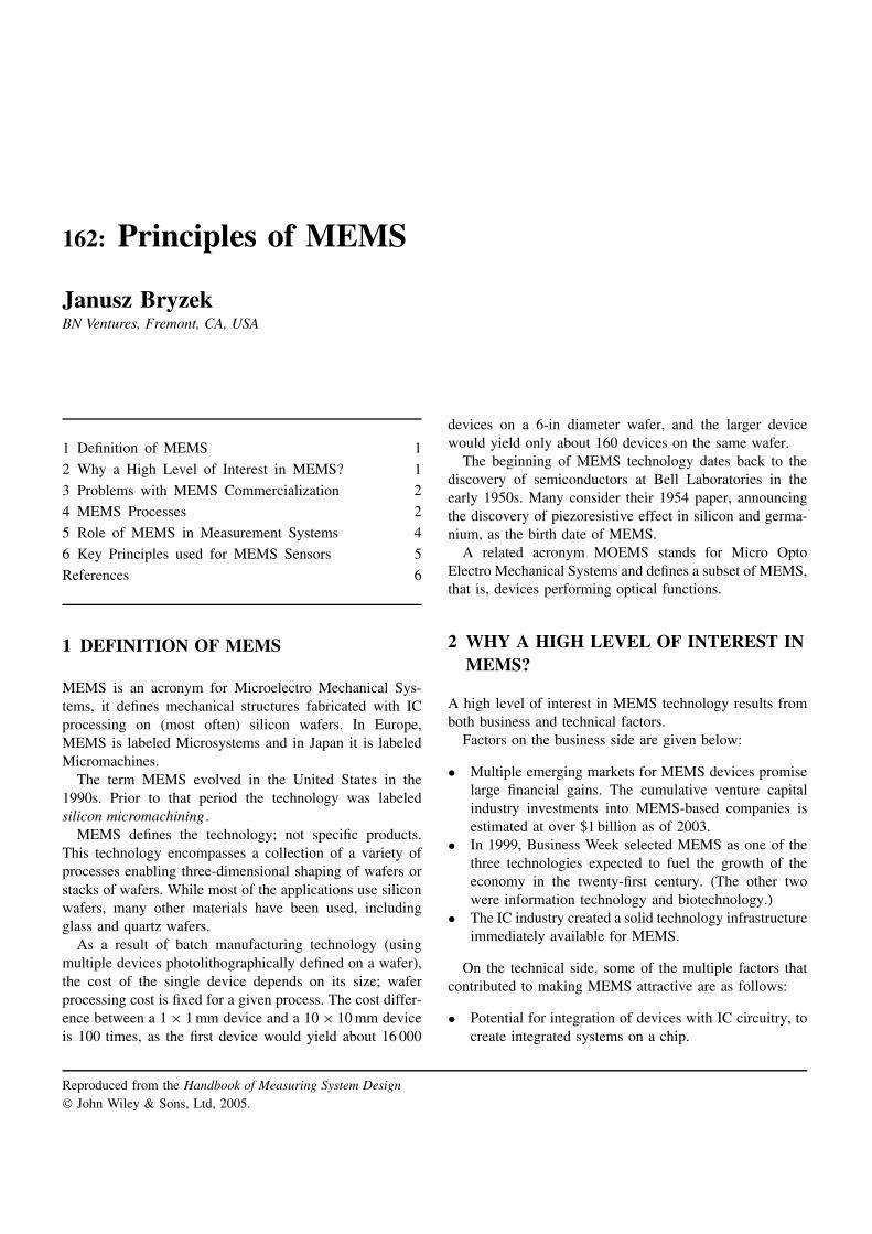
Figure 1. Scanning electron microscope (SEM) close-up of awafer showing photolithographically defined and etched patternforming part of the mirror array (1 mm each), contrasted insize with that of an ant. (With permission from TransparentNetworks, Inc.)
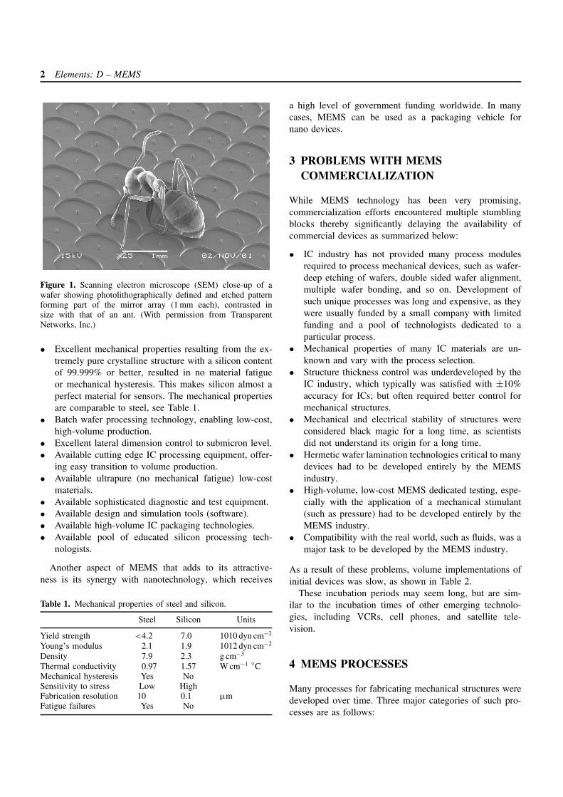
• Excellent mechanical properties resulting from the ex-tremely pure crystalline structure with a silicon contentof 99.999% or better, resulted in no material fatigueor mechanical hysteresis. This makes silicon almost aperfect material for sensors. The mechanical propertiesare comparable to steel, see Table 1.
• Batch wafer processing technology, enabling low-cost,high-volume production.
• Excellent lateral dimension control to submicron level.• Available cutting edge IC processing equipment, offer-
ing easy transition to volume production.• Available ultrapure (no mechanical fatigue) low-cost
materials.• Available sophisticated diagnostic and test equipment.• Available design and simulation tools (software).• Available high-volume IC packaging technologies.• Available pool of educated silicon processing tech-
nologists.
Another aspect of MEMS that adds to its attractive-ness is its synergy with nanotechnology, which receives
Table 1. Mechanical properties of steel and silicon.
Steel Silicon Units
Yield strength <4.2 7.0 1010 dyn cm−2
Young’s modulus 2.1 1.9 1012 dyn cm−2
Density 7.9 2.3 g cm−3
Thermal conductivity 0.97 1.57 W cm−1 ◦CMechanical hysteresis Yes NoSensitivity to stress Low HighFabrication resolution 10 0.1 µmFatigue failures Yes No
a high level of government funding worldwide. In manycases, MEMS can be used as a packaging vehicle fornano devices.
3 PROBLEMS WITH MEMSCOMMERCIALIZATION
While MEMS technology has been very promising,commercialization efforts encountered multiple stumblingblocks thereby significantly delaying the availability ofcommercial devices as summarized below:
• IC industry has not provided many process modulesrequired to process mechanical devices, such as wafer-deep etching of wafers, double sided wafer alignment,multiple wafer bonding, and so on. Development ofsuch unique processes was long and expensive, as theywere usually funded by a small company with limitedfunding and a pool of technologists dedicated to aparticular process.
• Mechanical properties of many IC materials are un-known and vary with the process selection.
• Structure thickness control was underdeveloped by theIC industry, which typically was satisfied with ±10%accuracy for ICs; but often required better control formechanical structures.
• Mechanical and electrical stability of structures wereconsidered black magic for a long time, as scientistsdid not understand its origin for a long time.
• Hermetic wafer lamination technologies critical to manydevices had to be developed entirely by the MEMSindustry.
• High-volume, low-cost MEMS dedicated testing, espe-cially with the application of a mechanical stimulant(such as pressure) had to be developed entirely by theMEMS industry.
• Compatibility with the real world, such as fluids, was amajor task to be developed by the MEMS industry.
As a result of these problems, volume implementations ofinitial devices was slow, as shown in Table 2.
These incubation periods may seem long, but are sim-ilar to the incubation times of other emerging technolo-gies, including VCRs, cell phones, and satellite tele-vision.
4 MEMS PROCESSES
Many processes for fabricating mechanical structures weredeveloped over time. Three major categories of such pro-cesses are as follows:

Principles of MEMS 3
Table 2. Development of MEMS.
Product First prototype Cum volume 1 M Incubation (years)
Pressure sensor 1961 1984 23Acceleration sensor 1970 piezoresistive 1995 25
1977 capacitive 1995 18Ink jet printers 1977 1996 19Displays (DLP) 1979 2001 22
• bulk micromachining of silicon• surface micromachining• deep reactive ion etching.
4.1 Isotropic etching
Bulk micromachining makes use of the entire wafer thick-ness, which typically may range from 500 to 1000 µm.
The first bulk micromachining process made use of theanisotropic wet etch developed for pressure sensors in 1970by Kulite, New Jersey. This etch could remove silicon in alldirections, independently, according to the crystallographicorientation of the substrate. The shape was defined by amasking process, Figure 2. The accuracy of the structuredefinition was not very good, as it depended on many fac-tors, such as time, temperature, and etchant concentration.No good etch-stop technology enabling termination of theetch at a predefined depth was developed.
4.2 Anisotropic etching
A major improvement in accuracy of etching was achievedwith the development of anisotropic wet etching, whichrelied on crystallographic orientation. This was first
Figure 2. Example of isotropic etching of silicon through across-shaped mask and with nonetched surface layer of siliconoxide. (With permission from Transparent Networks, Inc.)
demonstrated by Kulite, in New Jersey, in 1976 for pres-sure sensors. Different crystallographic directions of siliconexhibited different etch rates for selected etchants, suchas KOH. The etched rates could differ by 2 orders ofmagnitudes (depending on the direction); thus, the maskwas defining the shape of the etched cavity, with the onlyvariable being the depth. This depth still depended on tem-perature and concentration and could be controlled to about±10% of etched depth in the best cases. If the startingwafer thickness was 600 µm and etch depth was 500 µm,this meant the variation of thickness of unetched siliconwould be 100 ± 100 µm, or 0 to 200 µm. This was notgood enough for the first application, that is, in pressuresensors, as pressure sensitivity varies as the square (forpiezoresistive sensors) or cube (for capacitive sensors) ofthe diaphragm thickness.
Several techniques for stopping the etch on this layerwere later developed. One of them took the advantageof the high differential etch rate as a function of thesilicon-doping level: for high doping, the etch rate wassignificantly slower as compared to the low doping level.Using diffusion or ion implantation, a thin (submicronto tens of microns) highly doped (carrier concentration>1019 cm−3) surface layer could be formed, which wouldterminate the etch. The depth accuracy of such a layerwas still about ±10%, but the tolerance of the intendedfeature was not dependent on the etched thickness. If 5-µm thickness was programmed, it would have ±0.5-µmtolerance, which was not achievable without the etch stop.This type of etch stop was deployed (among others) inGeneral Motors pressure sensors, Figure 3.
Another etch-stop technique was based on the p-n junc-tion, biased by the voltage. During the initial etch, the p-njunction was blocking the flow of the current. As soon asone of the layers (p or n) was etched, the current flowcaused oxidation of the exposed area, stopping the etch.This type of etch stop was deployed (among others) byNovaSensor, California.
4.3 Sacrificial etching
Surface micromachining focused on using the few micronthick surface layer of the wafer, to simplify cointegration

4 Elements: D – MEMS
Figure 3. Anisotropic etching of silicon follows crystallographicplanes, enabling precision control of the rectangular patterns andformation of thin membranes. With etch stop, the thickness of thethin membrane (on the bottom of the chip) could be controlled toless than 10%. (With permission from Transparent Networks, Inc.)
with electronics. The process emerged through the 1980s,with major progress in its development at the UC Berkeleyand Sandia National Laboratories (2004).
The principle of sacrificial etching is based on siliconoxide etchants that do not etch polysilicon. The structuresare formed by patterning a layer of oxide into the requiredshape by photolithography, covering it with patterned layersof polysilicon, and then etching away (sacrificing) the oxidethrough small holes etched in polysilicon.
The thickness of structures fabricated with surface micro-machining is typically under 4 µm, due to limitations inpolysilicon deposition. One of the highest volume productsbased on this technology is the family acceleration sensorfrom Analog Devices, Massachusetts.
A well-advanced process is Summit V, developed at San-dia National Labs, enabling five layers of polysilicon to beindependently shaped to create complex mechanical sys-tems in the chip, such as gears, pumps, and mirrors – seeFigure 4.
4.4 Deep reactive ion etching (DRIE)
None of the deep wet etch technologies are friendly tothe processing of integrated circuits. Furthermore, slopingsilicon in an anisotropic etch unproductively consumes thechip area, thus, increasing its cost.
Development of plasma-based deep etching was a dreamtool for the MEMS industry. This tool emerged in the1990s, with major progress contributed by Bosch. Theirprocess was based on alternating two cycles: plasma etchingand vertical polymer wall coating to prevent lateral etching.
Initial etch speed was about 1 µm min−1. As of 2004, thefastest machines can deliver up to 10 µm min−1 rough etch(dimensions are not very well controlled).
While this deep reactive ion etching (DRIE) etches sili-con, its etch rate of silicon oxide is 100 to 1000 times slower
Polysilicon
1. Resist exposure
4. Resist exposure
Oxide
Oxide
Oxide
Resist
Resist
Mask
Mask
Substrate
2. Resist development and oxide etch
3. Deposition of polysilicon
Suspendedbeam
Anchor
6. Sacrificial etching of oxide
5. Resist development and polysilicon etch
Figure 4. Foundation for surface micromachining is sacrificialetching of silicon oxide underneath of polysilicon, to createsuspended mechanical structures. (Courtesy of Nadim Maluf,New Focus.)
(depending on settings), enabling creation of the etch stopon the oxide. One of the easiest approaches is the use ofsilicon on insulator (SOI) wafers, containing an embeddedlayer of oxide.
While the etch speed for DRIE is now comparable toanisotropic etch, the throughput is not. DRIE equipmentcan etch only one wafer at a time, while wet etching cansimultaneously process a large number of wafers (e.g. 100),limited only by inexpensive tooling.
If the design needs several DRIE etches with a cumula-tive depth of 800 µm (typical for many sensors), and theeffective (accuracy limited) etch speed of 4 µm min−1, eachwafer will use an etcher for 200 min. This allows etchingof only 7 wafers per day using three shifts, or about 1800wafers per year, in a 5-day week. This makes DRIE a signif-icantly more expensive process than wet etching. Examplesare shown in Figure 5.
5 ROLE OF MEMS IN MEASUREMENTSYSTEMS
MEMS-based devices play a valuable and instrumental rolein the sensor world, in their application in the measure-ment of physical variables. Key MEMS sensors include

Principles of MEMS 5
(a)
(b)
Figure 5. Deep reactive ion etching (DRIE) enables high aspectratio vertical etching of silicon. (a) SEM picture shows 1-µmwide, 30-µm deep silicon springs with 1-µm spacing betweensprings. (b) Close-up of the vertical wall, showing the surfacescalloping resulting from the alternative etching and polymerdeposition during the DRIE process. As shown, each cycle etchesapproximately 0.3 µm of silicon, resulting in highly vertical etch.(With permission from Transparent Networks, Inc.)
the following:
• Pressure: with MEMS sensors representing over 90%of units and 50% of revenues.
• Acceleration: with MEMS sensors representing over95% of units and 25% of revenues.
• Rate: with MEMS sensors representing about 95% ofunits and 75% of revenues.
• Force: with MEMS sensors representing about 20% ofunits and 5% of revenues.
Pressure sensors were the first devices based on silicontechnology introduced to the market in the 1960s, for mil-itary and aerospace applications. In the year 2003, the vol-ume of pressure sensors produced approached 200 millionunits, with automotive (most models of advanced cars
use over 10 pressure sensors) and medical (primarily dis-posable blood pressure sensors) markets dominating theunit volume.
Acceleration and gyro MEMS-based sensors were devel-oped for military and aerospace market in the 1970s. In theyear 2003, over 100 million units were produced and it wasdominated by the automotive airbag applications.
MEMS rate sensors were developed in the 1990s, firstfor military, and then for automotive applications. In 2003,their unit volume was about 2 million units. The largestvolume markets are automotive (stability control and GPS)and consumer (camera shake stabilization and cell phoneGPS), with the potential for 10 million rate sensors by 2010.
The major market for silicon force sensors are homescales, absorbing millions of devices.
The emerging MEMS sensing applications include thefollowing:
• infrared• flow• chemical• biological.
6 KEY PRINCIPLES USED FOR MEMSSENSORS
Major sensing technologies that can be applied in theMEMS form include the following:
• piezoresistive• capacitive• resonant• thermoelectric.
The piezoresistive effect (Smith, 1954) in silicon pro-duces resistance change that is approximately 2 ordersof magnitude larger when compared to the change thatwould result from a dimension change under applied stress(typical for metals). For example, if the material is elon-gated 0.1% by stretching, typical metallic resistors used forstrain gauges would change by about 0.2%, but the resis-tance of silicon would change by about 10%. Piezoresistivesensors dominate pressure, acceleration, and force appli-cations. Typically, four piezoresistors are connected intoa Wheatstone bridge configuration to reduce temperatureerrors. Figure 6 is a simple example of a piezoresistancesensor.
Capacitive sensors have at least one electrode movingunder the input variable, which typically would be pressure,acceleration, or rate. While the simplest configuration is twoflat electrode capacitors, the interdigitated silicon fingers(Figure 7), gained wide acceptance as an inertial sensor, asit allows for larger sensing capacitance.

6 Elements: D – MEMS
Force orpressure
Silicon beam or membranePiezoresistor(s)
R
Figure 6. Sensing piezoresistor schematic.
Resonant sensors are based on resonating beams ordiaphragms. Applied strain changes the resonant frequency(similar to a guitar string), enabling measurement of inputvariables such as pressure, acceleration, rate, and tempera-ture. Resonant frequency pickup may use any of the sensingtechnologies.
MEMS thermoelectric sensors are based on a large num-ber of tiny thermocouples connected in series. These areprimarily used to measure IR radiation. One end of thethermocouple is located over a thermally isolated region ofthe chip, the other end over conducting silicon. In responseto radiation, the thermally isolated end of the thermocouplegets warmer, enabling measurement of IR power.
The emerging approach for both chemical and biologicalMEMS sensors is based on carbon nanotube technology,demonstrated by Silicon Valley companies; it has greatpotential for creating new markets for yet more MEMSsensors.
Force orpressure
Electric isolation
Platecapacitor
Force orpressure
Combcapacitor
Silicon beam or membrane
Figure 7. Capacitive sensing schematic.
REFERENCES
Sandia National Labs, (2004) http://www.sandia.gov/mstc/technologies/micromachines/tech-info/technologies/summit5.html.
Smith, C.S. (1954) Piezoresistive Effect in Germanium and Sili-con. Physical Review, 94, 42–49.