Embed Size (px)
Citation preview

Study of Fracture Mechanics in Testing Interfacial Fractureof Solder Joints
W.H. BANG,1,2 M.-W. MOON,1 C.-U. KIM,2,4 S.H. KANG,1 J.P. JUNG,3
and K.H. OH1
1.—School of Materials Science and Engineering, Seoul National University, Seoul 151-742,Korea. 2.—Department of Materials Science and Engineering, University of Texas at Arlington,Arlington, TX, USA. 3.—Department of Materials Science and Engineering, University of Seoul,Seoul 130-743, Korea. 4.—e-mail: [email protected]
This paper is concerned with the mechanics of interfacial fracture that areactive in two common testing configurations of solder joint reliability. Utiliz-ing eutectic Pb-Sn/Cu as a reference system and assuming the presence of apredefined crack size in the intermetallic compound (IMC) layer, stressintensity factors (KI and KII) at the crack are numerically calculated for thetwo given configurations. The analysis of the tensile test configuration revealsthat the fracture occurs by the crack-opening mode (KI mode), as anticipated,but that it is greatly assisted by the viscoplasticity of the solder. With non-uniform viscoplastic deformation across the joint, KI is found to increase muchmore rapidly than it would without the solder, decreasing the critical cracksize to the micron scale. The same mechanism is also responsible for thedevelopment of a KII comparable to KI at the crack tip, that is, |KI/KII| � 1. Itis also found that the predominant fracture mode in the bump shear config-uration is crack opening, not crack shearing. This is an unexpected result, butnumerical analyses as well as experimental observations provide consistentindications that fracture occurs by crack opening. During shear testing, bumprotation due to nonzero rotational moment in the test configuration is found tobe responsible for the change in the fracture mode because the rotation makesKI become dominant over KII. With rotational moment being affected by thegeometry of the bump, it is further found that the fracture behavior may varywith bump size or shape.
Key words: Solder joint reliability, intermetallic layer, tensile test, bumpshear test, stress intensity factors (KI and KII)
INTRODUCTION
Sn-based solder alloys are widely used in elec-tronic packaging applications as they offer severaladvantageous properties, including low processingtemperatures and excellent wetting of common Cumetallization components. With the continuingthrust toward smaller and higher-performancepackaging, however, the alloys are becoming asource of critical reliability concerns. In advanced
packaging, solder joints are required to endureincreasingly punishing mechanical load conditions,and thus they are increasingly prone to physicalfailures. Of these physical reliability failures, one ofthe most troubling is fracture at the interface be-tween solder and metallization. The interface isknown to be the weakest mechanical link in allsolder joints because the presence of brittle Sn-Cuintermetallic compounds (IMC, Cu6Sn5 or Cu3Sn)weakens the overall resistance against fracture andalso creates a point of stress singularity at whichcracks can initiate.1–6 In order to enhance theoverall reliability of the solder joint, it is therefore(Received April 13, 2007; accepted January 16, 2008;
published online February 13, 2008)
Journal of ELECTRONIC MATERIALS, Vol. 37, No. 4, 2008 Special Issue Paper
DOI: 10.1007/s11664-008-0393-8� 2008 TMS
417
critical to prevent or retard the interface fracture,and this has been the main focus of recent studies inthis field. Progress in this area demands a more in-depth investigation of interface fracture mechanics.
There are two common methods of characterizingthe mechanics of interface fracture: the joint tensiletest and the bump shear test.5,7–10 The tensile testrequires the induction of interfacial fracture byexerting a load in a direction normal to the inter-facial layer, while the bump shear test requires theapplication of a force in a direction parallel to theinterfacial layer. The simplicity of these methods,combined with their ability to provide quantitativeinformation and fractography, has made them themost popular approaches for the investigation ofinterface fracture in solder joints. However, suchstudies produce data with clear limitations. Realsolder joints are subjected to complex load condi-tions and, as a result, their fracture may proceed bysignificantly different mechanisms than the onesfound in the tensile or bump shear test. Further,because of the time-dependent mechanical proper-ties of the solder, the fracture mechanism underdiffering load conditions of a single test method(bump shear or tensile joint) may be sufficientlydifferent to lead to the need for nonsimplisticmethods of analysis. In order to extrapolate infor-mation from the common test configurations to realsolder joints, it is imperative to investigate morecarefully how fracture occurs in each of these twomethods. This quest requires the study of fracturemechanics in the IMC layer to determine the frac-ture criteria, including the critical crack size andthe fracture mode under a given load condition.11,12
This paper presents the results of our investiga-tion on the interface fracture mechanics of the bumpshear and joint tensile test methods. Specifically,this paper investigates the fracture mode by con-ducting numerical analysis of the stress intensityfactors (K) at the crack tip in the IMC layer for eachmethod. The cases simulated here are fractures atthe brittle IMC layer created by a reaction betweenthe Sn-Pb eutectic solder and Cu substrate undergeometrical constraints and load conditions rele-vant to the tensile test and a bump shear test. Ouranalysis yields several interesting and somewhatsurprising results of practical importance. We findthat the fracture behavior for the two methods, thatis, the crack-opening (KI) mode for the tensile andthe crack-shearing mode (KII) for the bump sheartesting, are not as simple as each method intends to
produce. In the case of the tensile test condition, it isfound that the viscoplastic deformation and Poissoncontraction of the solder matrix have a significantinfluence on the stress field around the crack tip.With viscoplastic deformation of the solder, KI in-creases much more rapidly than without solder,making the IMC more prone to cracking. Further-more, Poisson contraction causes the crack in theIMC to develop a KII value with a magnitude com-parable to that of KI. Even more unexpected is theresult that the crack propagation in the bump sheartest condition occurs by the KI mode not by the KII
mode. It is found that the KI mode prevails becauseof bump rotation during crack propagation. Thisresult is surprising but our experimental investi-gation produces supporting evidence. The rotationof solder bumps in the shear direction is clearlyseen, resulting in the fracture site being lifted upfrom the substrate and the development of crackopening (KI) during shearing. These results stronglysuggest that any characterization of the interfacefracture of solder joint, especially characterizationconducted with the two common methods, needs toinclude careful consideration of the solder defor-mation and rotation with variations in geometricaland load conditions.
BACKGROUND AND NUMERICAL ANDEXPERIMENTAL PROCEDURES
Background
While there exist a few experimental results forsolder joint fracture in tensile tests, the study of Sn-Pb/Cu joints is most comprehensive and thus pro-vides the data needed for our modeling work. Thedata used in our modeling is taken from Sn-Pb/Cutensile testing conducted by Lee et al., Prakashet al., and Quan.7–9 Table I shows the summary ofthe tensile test data along with the experimentalconditions used in these studies. While there aredifferences in the experimental details, such as thetension rate and specimen configuration, the testsshow reasonable agreement in the fracture strengthvalue of �80 MPa. In spite of this agreement,Prakash et al. and Quan report somewhat differentobservations on the crack propagation path. Quannotes that the fracture proceeds through the IMClayer (Cu6Sn5) and therefore attributes the data tothe fracture strength of the IMC layer. On the otherhand, Prakash et al. suggest, based on the fractog-raphy showing the mixture of IMC and solder
Table I. Tensile Testing Results of Cu/Sn-Pb/Cu Joints (As-Soldered Samples)
FractureStrength
JointThickness
Cross Sectionof Joint
TensioningRate
IMCThickness
Lee et al.7 77 MPa 750 lm 3 mm (diameter) 0.6 mm/min �1 lmPrakash et al.8 86 MPa 200 � 300 lm 10 mm · 3 mm 0.5 mm/min (0.66 MPa/s) 2.5 lmQuan9 83 MPa 1.0 mm 7.6 mm · 2.8 mm 0.05 mm/min (0.47 MPa/s) 1 � 3 lm
Bang, Moon, Kim, Kang, Jung, and Oh418
matrix, that the measured fracture strength may berelated to the decohesion strength between the sol-der and the IMC layer. However, since such frac-tography can result from the cracks repeatedlyswitching between the solder and the IMC layer,and in such cases the brittle IMC phase would limitthe overall fracture strength of the joints, it seemsreasonable to assume that the measured fracturestrength is attributable to the fracture strength ofthe IMC layer. The tensile load (stress)–displace-ment (strain) curves presented by Prakash et al.and Quan also provide supporting evidence for thisassessment. In both cases, an abrupt drop in loadafter its maximum is visible. This is not possiblewithout rapid crack growth through a brittle phase.
While numerous studies using the bump shearmethod have correlated the test results to IMCfracture, the resulting data requires considerationof its complexity. The difficulty of analyzing thefracture mechanics of this method stems mainlyfrom the fact that the test load is imparted to theinterface area through a bump that is softer thanthe IMC phase at the interface. As is well pointedout by Huang et al. and Kim et al. in their finiteelement method (FEM) analysis,13,14 the visco-plasticity of the bump in such a case may play acritical role in the fracture at the interface. Per-haps more importantly, shearing load, impartingnonzero rotational momentum to the bump, mayresult in physical motion of the bump that changesthe mechanical constraints at the crack tip. Thispossibility has been proven to exist in our experi-mental and numerical studies. It is thereforenecessary for fracture analysis to include consid-eration of the viscoplasticity as well as the bumpmovement.
FEM Modeling
Our numerical analysis of the fracture mechanicsbegins with the assumption that the fracture initi-ates and proceeds predominantly through the brit-tle IMC layer in both configurations, which is areasonable assumption as previously mentioned.Consequently, the modeling requires calculation ofthe stress intensity factors, K, at the crack tip in theIMC layer under the two different test configura-tions while the fracture strength of the IMC layer isset to 80 MPa. For this numerical analysis, we use acommercial FEM program, ABAQUS 6.3 with thefinite element mesh structure shown in Fig. 1a andb. As is shown in these figures, the IMC layer be-tween the eutectic Sn-Pb solder and Cu is assumedto be 1-lm-thick Cu6Sn5.2,9 Table II lists themechanical properties of the materials used in ourFEM analysis. It is further assumed that the test isconducted at room temperature, �300 K, in order tobe consistent with the existing data and commontesting practice. This temperature is a high homol-ogous temperature for eutectic Sn-Pb solder,�0.65Tm, and thus the viscoplastic characteristicsof eutectic Sn-Pb are incorporated into the finite
element calculation. The viscoplastic constitutiveequation used is:
_epl ¼ 2:68� 102 � ½r�3:2 � exp � 69 kJ=mol
RT
� �
þ 1:38� 10�6 � ½r�6:2 � exp � 64 kJ=mol
RT
� �;
(1)
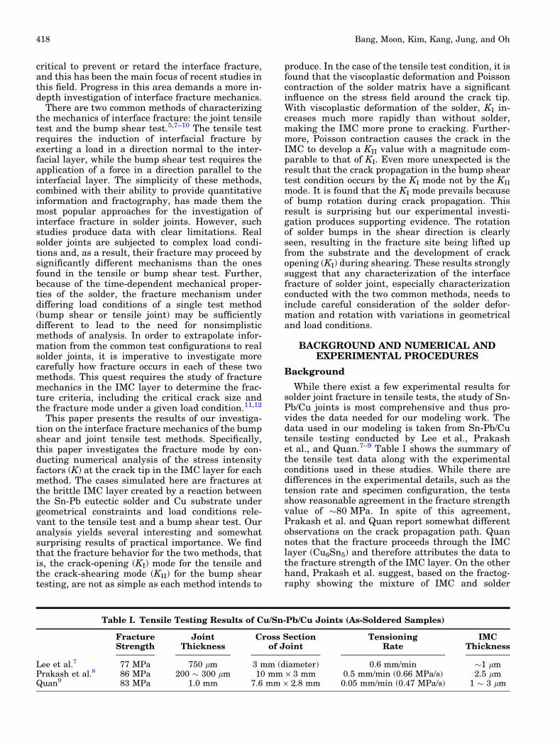
Fig. 1. Finite element models and crack mesh for estimatingstress intensity factors, K, at the crack tip in the IMC layer duringjoint tensile and bump shear tests: (a) FEM meshes for jointtensile analyses; (b) FEM meshes for bump shear analyses withcalculations performed for different bump sizes, R; and (c) thecrack tip mesh defined in the IMC layer in the dashed-circle areain (a) and (b).
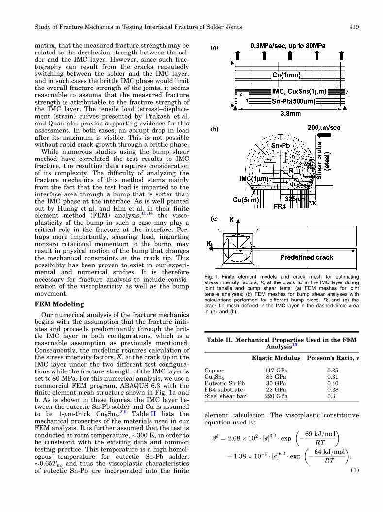
Table II. Mechanical Properties Used in the FEMAnalysis15
Elastic Modulus Poisson�s Ratio, m
Copper 117 GPa 0.35Cu6Sn5 85 GPa 0.31Eutectic Sn-Pb 30 GPa 0.40FR4 substrate 22 GPa 0.28Steel shear bar 220 GPa 0.3
Study of Fracture Mechanics in Testing Interfacial Fracture of Solder Joints 419
where _epl is the plastic strain rate, r (MPa) is thestress, R is the gas constant, and T is the temper-ature.16 Figure 1c shows the mesh structure for apredefined crack in the IMC layer for the calculationof the stress intensity factors in the joint tensile andbump shear tests. The K factors are evaluated atfive finite element contours surrounding the crackfront from one crack face to the opposite crackface.17 The detailed description of Fig. 1a–c and ourFEM analysis procedure follow.
Tensile Analysis
The two-dimensional finite elements in Fig. 1aare a simplification of the butt-joined tensile speci-men used in Quan�s experiment.9 A quarter sectionis modeled using symmetric boundary conditionsalong the transverse and longitudinal directions.Considering the fact that the specimen width is fargreater than the joint thickness, a plane-straincondition is employed.9,18,19 From the tensile-loaddevelopment curve and data presented by Quan, theapplied tensile rate was determined to be 0.3 MPa/sand this value is used for our main calculation.Further, since the outer edge of the joint is the mostlikely place for crack initiation, being subjected tothe highest interfacial stress singularity,6,20 thecrack tip mesh in the IMC layer is placed at the end(indicated by a dashed circle in Fig. 1a). In this way,the calculation of the K factors with variation in thesize of predefined crack is performed.
Bump Shear Analysis
The finite element model in Fig. 1b is a crosssection of a eutectic Sn-Pb bump reflowed on acopper pad. The crack mesh in the IMC layer isdefined at the bump corner (indicated as a dashedcircle in Fig. 1b), as this is the expected place forcrack initiation. The development of the K factorswith shear displacement is calculated for a givensize of predefined crack. In our calculation, theinterfacial area is fixed and we include the shapeand size of the bump as variables, as they may varyin real testing situations and also have a significantinfluence on shear stress development at the cracktip. Table III details the shape and size of the bumpconsidered in our simulation, expressed in terms of
the geometrical parameters U, DX, and R. The def-inition of these parameters can be found in Fig. 1b.The key variation in these parameters is the radiusR. The others are adjusted based on the wettingbehavior of the bump for the given size of theinterfacial area.
Bump Shear Test
Instead of analyzing published data, we con-ducted the bump shear test for a selected case inorder to acquire the information needed for ouranalysis. This test is especially necessary to identifyany bump motion during the test. For this test, weprepared the eutectic Sn-Pb bump shear samplesfollowing standard procedures. The solder ballsused in our experiment had a diameter of 760 lm.The balls are attached to the 650-lm-diameter Cupad by reflow treatment at 215�C for �1 min. Theywere then subjected to the shear test while the loadand displacement are recorded. For selected cases,position markers, in the form of small indentations,were made on top of the bump before shear testingfor the purpose of tracing the bump movement.These markers, consisting of three consecutiveindentations along the centerline of the bump, weremade by creating a small impression using a micro-indenter. The marker position was then comparedbefore and after shear testing using scanning elec-tron microscopy (SEM, refer to Fig. 8).
RESULTS
Fracture Analysis in Joint Tensile
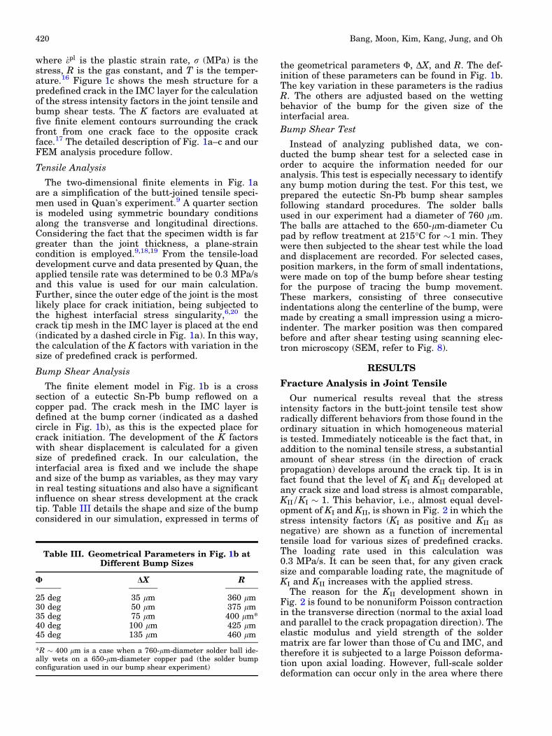
Our numerical results reveal that the stressintensity factors in the butt-joint tensile test showradically different behaviors from those found in theordinary situation in which homogeneous materialis tested. Immediately noticeable is the fact that, inaddition to the nominal tensile stress, a substantialamount of shear stress (in the direction of crackpropagation) develops around the crack tip. It is infact found that the level of KI and KII developed atany crack size and load stress is almost comparable,KII/KI � 1. This behavior, i.e., almost equal devel-opment of KI and KII, is shown in Fig. 2 in which thestress intensity factors (KI as positive and KII asnegative) are shown as a function of incrementaltensile load for various sizes of predefined cracks.The loading rate used in this calculation was0.3 MPa/s. It can be seen that, for any given cracksize and comparable loading rate, the magnitude ofKI and KII increases with the applied stress.
The reason for the KII development shown inFig. 2 is found to be nonuniform Poisson contractionin the transverse direction (normal to the axial loadand parallel to the crack propagation direction). Theelastic modulus and yield strength of the soldermatrix are far lower than those of Cu and IMC, andtherefore it is subjected to a large Poisson deforma-tion upon axial loading. However, full-scale solderdeformation can occur only in the area where there
Table III. Geometrical Parameters in Fig. 1b atDifferent Bump Sizes
U DX R
25 deg 35 lm 360 lm30 deg 50 lm 375 lm35 deg 75 lm 400 lm*40 deg 100 lm 425 lm45 deg 135 lm 460 lm
*R � 400 lm is a case when a 760-lm-diameter solder ball ide-ally wets on a 650-lm-diameter copper pad (the solder bumpconfiguration used in our bump shear experiment)
Bang, Moon, Kim, Kang, Jung, and Oh420
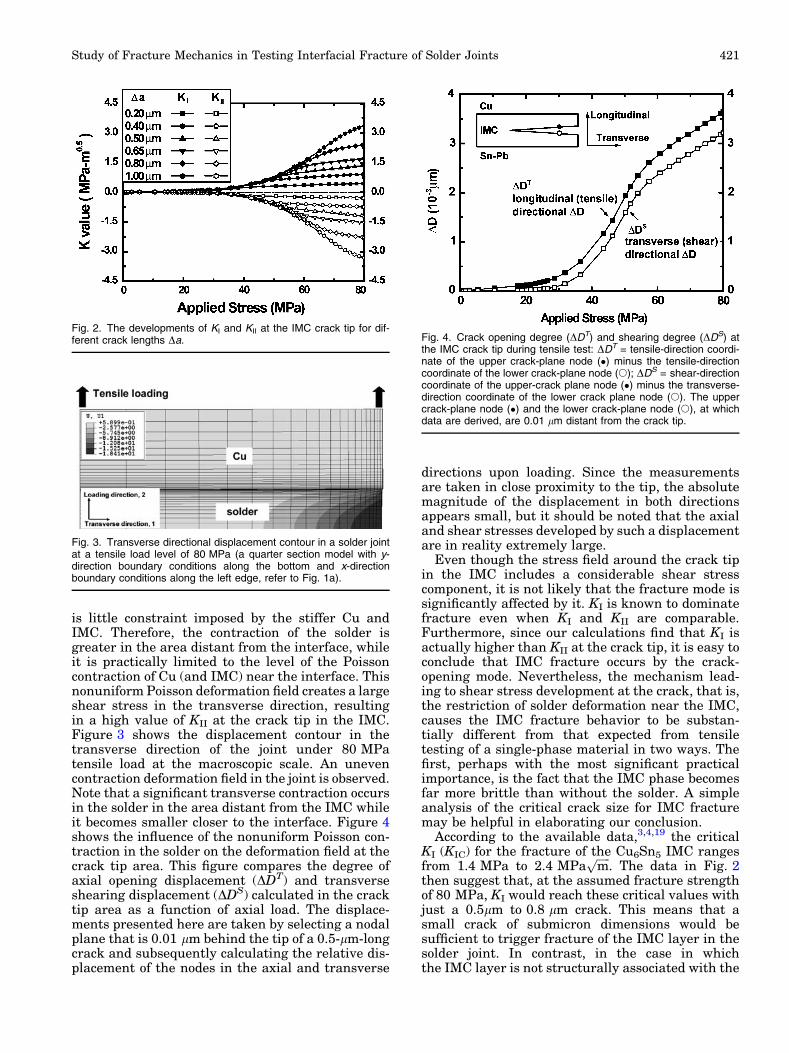
is little constraint imposed by the stiffer Cu andIMC. Therefore, the contraction of the solder isgreater in the area distant from the interface, whileit is practically limited to the level of the Poissoncontraction of Cu (and IMC) near the interface. Thisnonuniform Poisson deformation field creates a largeshear stress in the transverse direction, resultingin a high value of KII at the crack tip in the IMC.Figure 3 shows the displacement contour in thetransverse direction of the joint under 80 MPatensile load at the macroscopic scale. An unevencontraction deformation field in the joint is observed.Note that a significant transverse contraction occursin the solder in the area distant from the IMC whileit becomes smaller closer to the interface. Figure 4shows the influence of the nonuniform Poisson con-traction in the solder on the deformation field at thecrack tip area. This figure compares the degree ofaxial opening displacement (DDT) and transverseshearing displacement (DDS) calculated in the cracktip area as a function of axial load. The displace-ments presented here are taken by selecting a nodalplane that is 0.01 lm behind the tip of a 0.5-lm-longcrack and subsequently calculating the relative dis-placement of the nodes in the axial and transverse
directions upon loading. Since the measurementsare taken in close proximity to the tip, the absolutemagnitude of the displacement in both directionsappears small, but it should be noted that the axialand shear stresses developed by such a displacementare in reality extremely large.
Even though the stress field around the crack tipin the IMC includes a considerable shear stresscomponent, it is not likely that the fracture mode issignificantly affected by it. KI is known to dominatefracture even when KI and KII are comparable.Furthermore, since our calculations find that KI isactually higher than KII at the crack tip, it is easy toconclude that IMC fracture occurs by the crack-opening mode. Nevertheless, the mechanism lead-ing to shear stress development at the crack, that is,the restriction of solder deformation near the IMC,causes the IMC fracture behavior to be substan-tially different from that expected from tensiletesting of a single-phase material in two ways. Thefirst, perhaps with the most significant practicalimportance, is the fact that the IMC phase becomesfar more brittle than without the solder. A simpleanalysis of the critical crack size for IMC fracturemay be helpful in elaborating our conclusion.
According to the available data,3,4,19 the criticalKI (KIC) for the fracture of the Cu6Sn5 IMC rangesfrom 1.4 MPa to 2.4 MPa
ffiffiffiffiffimp
. The data in Fig. 2then suggest that, at the assumed fracture strengthof 80 MPa, KI would reach these critical values withjust a 0.5lm to 0.8 lm crack. This means that asmall crack of submicron dimensions would besufficient to trigger fracture of the IMC layer in thesolder joint. In contrast, in the case in whichthe IMC layer is not structurally associated with the
Fig. 3. Transverse directional displacement contour in a solder jointat a tensile load level of 80 MPa (a quarter section model with y-direction boundary conditions along the bottom and x-directionboundary conditions along the left edge, refer to Fig. 1a).
Fig. 4. Crack opening degree (DDT) and shearing degree (DDS) atthe IMC crack tip during tensile test: DDT = tensile-direction coordi-nate of the upper crack-plane node (�) minus the tensile-directioncoordinate of the lower crack-plane node (s); DDS = shear-directioncoordinate of the upper-crack plane node (�) minus the transverse-direction coordinate of the lower crack plane node (s). The uppercrack-plane node (�) and the lower crack-plane node (s), at whichdata are derived, are 0.01 lm distant from the crack tip.
Fig. 2. The developments of KI and KII at the IMC crack tip for dif-ferent crack lengths Da.
Study of Fracture Mechanics in Testing Interfacial Fracture of Solder Joints 421
solder, the critical crack size is found to be muchlarger. If it is assumed that the IMC is purely elasticand tested as a homogeneous sample, the mode Istress intensity factor developed at the crack tipshould be given by r
ffiffiffiffiffipcp
. Under an identical frac-ture condition, that is KIC = 1.4 MPa to 2.4 MPa
ffiffiffiffiffimp
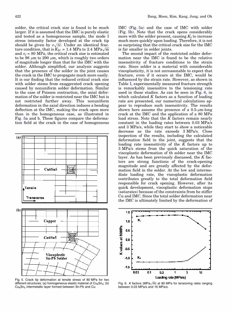
and rf = 80 MPa, the critical crack size is estimatedto be 98 lm to 290 lm, which is roughly two ordersof magnitude longer than that for the IMC with thesolder. Although simplified, our analysis suggeststhat the presence of the solder in the joint causesthe crack in the IMC to propagate much more easily.It is our finding that the reduced critical crack sizewith solder stems from exaggerated crack openingcaused by nonuniform solder deformation. Similarto the case of Poisson contraction, the axial defor-mation of the solder is restricted near the IMC but isnot restricted further away. This nonuniformdeformation in the axial direction induces a bendingdeflection at the IMC, making the crack open morethan in the homogeneous case, as illustrated inFig. 5a and b. These figures compare the deforma-tion field at the crack in the case of homogeneous
IMC (Fig. 5a) and the case of IMC with solder(Fig. 5b). Note that the crack opens considerablymore with the solder present, causing KI to increasemuch more quickly upon loading. Therefore, it is notso surprising that the critical crack size for the IMCis far smaller in solder joints.
The second impact of the restricted solder defor-mation near the IMC is found to be the relativeinsensitivity of fracture conditions to the strainrate. Since solder is a material with considerableviscoplasticity, it is not unreasonable to expect thatfracture, even if it occurs at the IMC, would beinfluenced by the strain rate. However, as shown inTable I, experimentally measured fracture strengthis remarkably insensitive to the tensioning rateused in these studies. As can be seen in Fig. 6, inwhich calculated K factors as a function of loadingrate are presented, our numerical calculations ap-pear to reproduce such insensitivity. The resultsshown here assume the presence of a 0.5-lm-longcrack at the IMC and the application of a 80 MPaload stress. Note that the K factors remain nearlyconstant in the loading rates between 0.03 MPa/sand 3 MPa/s, while they start to show a noticeabledecrease as the rate exceeds 3 MPa/s. Closeinspection of the results, including the calculateddeformation field in the joint, suggests that theloading rate insensitivity of the K factors up to3 MPa/s stems from the quick saturation of theviscoplastic deformation of th solder near the IMClayer. As has been previously discussed, the K fac-tors are strong functions of the crack-openingmagnitude and are greatly affected by the defor-mation field in the solder. At the low and interme-diate loading rate, the viscoplastic deformationcontributes greatly to the total deformation fieldresponsible for crack opening. However, after itsquick development, viscoplastic deformation stops(saturates) because of the constraints from he stifferCu and IMC. Since the total solder deformation nearthe IMC is ultimately limited by the deformation of
Fig. 6. K factors (MPaffiffiffiffimp
) at 80 MPa for tensioning rates rangingbetween 0.03 MPa/s and 16 MPa/s.
Fig. 5. Crack tip deformation at tensile stress of 80 MPa for twodifferent structures: (a) homogeneous elastic material of Cu6Sn5; (b)Cu6Sn5 intermetallic layer formed between Sn-Pb and Cu.
Bang, Moon, Kim, Kang, Jung, and Oh422
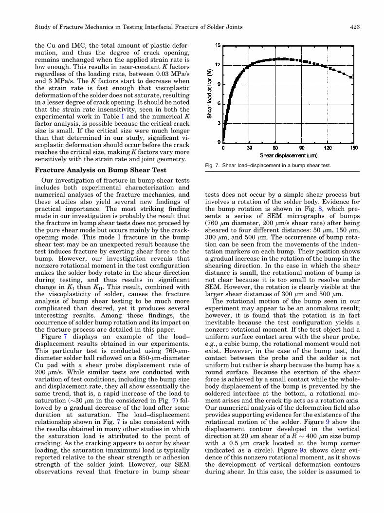
the Cu and IMC, the total amount of plastic defor-mation, and thus the degree of crack opening,remains unchanged when the applied strain rate islow enough. This results in near-constant K factorsregardless of the loading rate, between 0.03 MPa/sand 3 MPa/s. The K factors start to decrease whenthe strain rate is fast enough that viscoplasticdeformation of the solder does not saturate, resultingin a lesser degree of crack opening. It should be notedthat the strain rate insensitivity, seen in both theexperimental work in Table I and the numerical Kfactor analysis, is possible because the critical cracksize is small. If the critical size were much longerthan that determined in our study, significant vi-scoplastic deformation should occur before the crackreaches the critical size, making K factors vary moresensitively with the strain rate and joint geometry.
Fracture Analysis on Bump Shear Test
Our investigation of fracture in bump shear testsincludes both experimental characterization andnumerical analyses of the fracture mechanics, andthese studies also yield several new findings ofpractical importance. The most striking findingmade in our investigation is probably the result thatthe fracture in bump shear tests does not proceed bythe pure shear mode but occurs mainly by the crack-opening mode. This mode I fracture in the bumpshear test may be an unexpected result because thetest induces fracture by exerting shear force to thebump. However, our investigation reveals thatnonzero rotational moment in the test configurationmakes the solder body rotate in the shear directionduring testing, and thus results in significantchange in KI than KII. This result, combined withthe viscoplasticity of solder, causes the fractureanalysis of bump shear testing to be much morecomplicated than desired, yet it produces severalinteresting results. Among these findings, theoccurrence of solder bump rotation and its impact onthe fracture process are detailed in this paper.
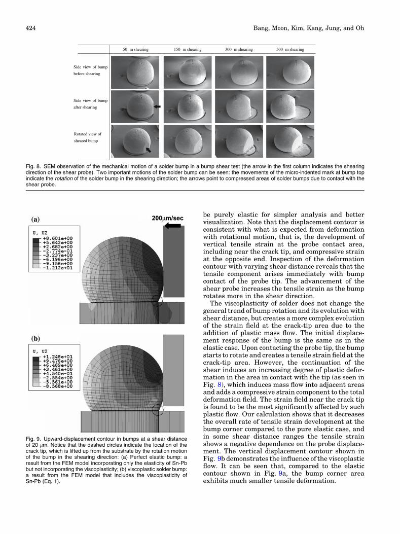
Figure 7 displays an example of the load–displacement results obtained in our experiments.This particular test is conducted using 760-lm-diameter solder ball reflowed on a 650-lm-diameterCu pad with a shear probe displacement rate of200 lm/s. While similar tests are conducted withvariation of test conditions, including the bump sizeand displacement rate, they all show essentially thesame trend, that is, a rapid increase of the load tosaturation (�30 lm in the considered in Fig. 7) fol-lowed by a gradual decrease of the load after someduration at saturation. The load–displacementrelationship shown in Fig. 7 is also consistent withthe results obtained in many other studies in whichthe saturation load is attributed to the point ofcracking. As the cracking appears to occur by shearloading, the saturation (maximum) load is typicallyreported relative to the shear strength or adhesionstrength of the solder joint. However, our SEMobservations reveal that fracture in bump shear
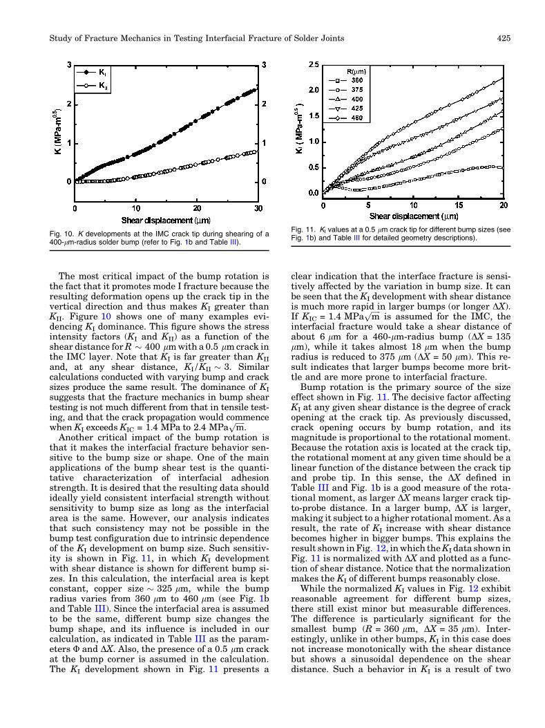
tests does not occur by a simple shear process butinvolves a rotation of the solder body. Evidence forthe bump rotation is shown in Fig. 8, which pre-sents a series of SEM micrographs of bumps(760 lm diameter, 200 lm/s shear rate) after beingsheared to four different distances: 50 lm, 150 lm,300 lm, and 500 lm. The occurrence of bump rota-tion can be seen from the movements of the inden-tation markers on each bump. Their position showsa gradual increase in the rotation of the bump in theshearing direction. In the case in which the sheardistance is small, the rotational motion of bump isnot clear because it is too small to resolve underSEM. However, the rotation is clearly visible at thelarger shear distances of 300 lm and 500 lm.
The rotational motion of the bump seen in ourexperiment may appear to be an anomalous result;however, it is found that the rotation is in factinevitable because the test configuration yields anonzero rotational moment. If the test object had auniform surface contact area with the shear probe,e.g., a cubic bump, the rotational moment would notexist. However, in the case of the bump test, thecontact between the probe and the solder is notuniform but rather is sharp because the bump has around surface. Because the exertion of the shearforce is achieved by a small contact while the whole-body displacement of the bump is prevented by thesoldered interface at the bottom, a rotational mo-ment arises and the crack tip acts as a rotation axis.Our numerical analysis of the deformation field alsoprovides supporting evidence for the existence of therotational motion of the solder. Figure 9 show thedisplacement contour developed in the verticaldirection at 20 lm shear of a R � 400 lm size bumpwith a 0.5 lm crack located at the bump corner(indicated as a circle). Figure 9a shows clear evi-dence of this nonzero rotational moment, as it showsthe development of vertical deformation contoursduring shear. In this case, the solder is assumed to
Fig. 7. Shear load–displacement in a bump shear test.
Study of Fracture Mechanics in Testing Interfacial Fracture of Solder Joints 423
be purely elastic for simpler analysis and bettervisualization. Note that the displacement contour isconsistent with what is expected from deformationwith rotational motion, that is, the development ofvertical tensile strain at the probe contact area,including near the crack tip, and compressive strainat the opposite end. Inspection of the deformationcontour with varying shear distance reveals that thetensile component arises immediately with bumpcontact of the probe tip. The advancement of theshear probe increases the tensile strain as the bumprotates more in the shear direction.
The viscoplasticity of solder does not change thegeneral trend of bump rotation and its evolution withshear distance, but creates a more complex evolutionof the strain field at the crack-tip area due to theaddition of plastic mass flow. The initial displace-ment response of the bump is the same as in theelastic case. Upon contacting the probe tip, the bumpstarts to rotate and creates a tensile strain field at thecrack-tip area. However, the continuation of theshear induces an increasing degree of plastic defor-mation in the area in contact with the tip (as seen inFig. 8), which induces mass flow into adjacent areasand adds a compressive strain component to the totaldeformation field. The strain field near the crack tipis found to be the most significantly affected by suchplastic flow. Our calculation shows that it decreasesthe overall rate of tensile strain development at thebump corner compared to the pure elastic case, andin some shear distance ranges the tensile strainshows a negative dependence on the probe displace-ment. The vertical displacement contour shown inFig. 9b demonstrates the influence of the viscoplasticflow. It can be seen that, compared to the elasticcontour shown in Fig. 9a, the bump corner areaexhibits much smaller tensile deformation.
Fig. 9. Upward-displacement contour in bumps at a shear distanceof 20 lm. Notice that the dashed circles indicate the location of thecrack tip, which is lifted up from the substrate by the rotation motionof the bump in the shearing direction: (a) Perfect elastic bump: aresult from the FEM model incorporating only the elasticity of Sn-Pbbut not incorporating the viscoplasticity; (b) viscoplastic solder bump:a result from the FEM model that includes the viscoplasticity ofSn-Pb (Eq. 1).
05 µ 051 gniraehs m µ 003 gniraehs m µ 005 gniraehs m µ gniraehs m
pmub fo weiv ediS
gniraehs erofeb
pmub fo weiv ediS
gniraehs retfa
d view ofetatoR
pmub deraehs
Fig. 8. SEM observation of the mechanical motion of a solder bump in a bump shear test (the arrow in the first column indicates the shearingdirection of the shear probe). Two important motions of the solder bump can be seen: the movements of the micro-indented mark at bump topindicate the rotation of the solder bump in the shearing direction; the arrows point to compressed areas of solder bumps due to contact with theshear probe.
Bang, Moon, Kim, Kang, Jung, and Oh424
The most critical impact of the bump rotation isthe fact that it promotes mode I fracture because theresulting deformation opens up the crack tip in thevertical direction and thus makes KI greater thanKII. Figure 10 shows one of many examples evi-dencing KI dominance. This figure shows the stressintensity factors (KI and KII) as a function of theshear distance for R � 400 lm with a 0.5 lm crack inthe IMC layer. Note that KI is far greater than KII
and, at any shear distance, KI/KII � 3. Similarcalculations conducted with varying bump and cracksizes produce the same result. The dominance of KI
suggests that the fracture mechanics in bump sheartesting is not much different from that in tensile test-ing, and that the crack propagation would commencewhen KI exceeds KIC = 1.4 MPa to 2.4 MPa
ffiffiffiffiffimp
.Another critical impact of the bump rotation is
that it makes the interfacial fracture behavior sen-sitive to the bump size or shape. One of the mainapplications of the bump shear test is the quanti-tative characterization of interfacial adhesionstrength. It is desired that the resulting data shouldideally yield consistent interfacial strength withoutsensitivity to bump size as long as the interfacialarea is the same. However, our analysis indicatesthat such consistency may not be possible in thebump test configuration due to intrinsic dependenceof the KI development on bump size. Such sensitiv-ity is shown in Fig. 11, in which KI developmentwith shear distance is shown for different bump si-zes. In this calculation, the interfacial area is keptconstant, copper size � 325 lm, while the bumpradius varies from 360 lm to 460 lm (see Fig. 1band Table III). Since the interfacial area is assumedto be the same, different bump size changes thebump shape, and its influence is included in ourcalculation, as indicated in Table III as the param-eters U and DX. Also, the presence of a 0.5 lm crackat the bump corner is assumed in the calculation.The KI development shown in Fig. 11 presents a
clear indication that the interface fracture is sensi-tively affected by the variation in bump size. It canbe seen that the KI development with shear distanceis much more rapid in larger bumps (or longer DX).If KIC = 1.4 MPa
ffiffiffiffiffimp
is assumed for the IMC, theinterfacial fracture would take a shear distance ofabout 6 lm for a 460-lm-radius bump (DX = 135lm), while it takes almost 18 lm when the bumpradius is reduced to 375 lm (DX = 50 lm). This re-sult indicates that larger bumps become more brit-tle and are more prone to interfacial fracture.
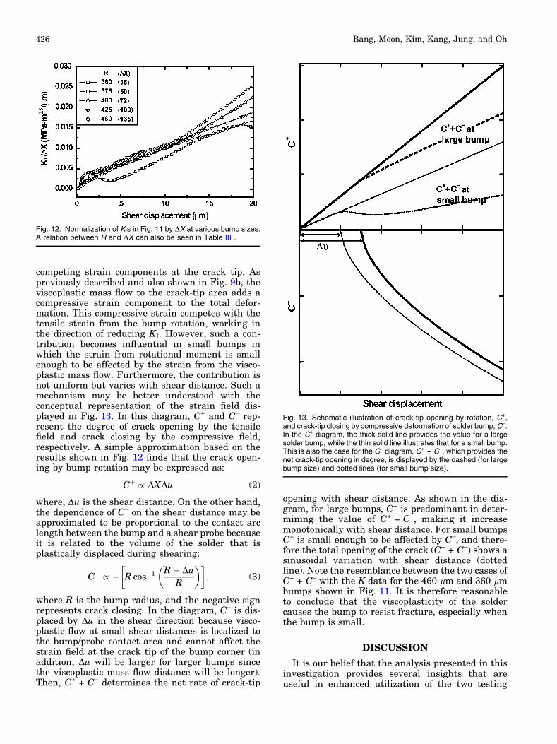
Bump rotation is the primary source of the sizeeffect shown in Fig. 11. The decisive factor affectingKI at any given shear distance is the degree of crackopening at the crack tip. As previously discussed,crack opening occurs by bump rotation, and itsmagnitude is proportional to the rotational moment.Because the rotation axis is located at the crack tip,the rotational moment at any given time should be alinear function of the distance between the crack tipand probe tip. In this sense, the DX defined inTable III and Fig. 1b is a good measure of the rota-tional moment, as larger DX means larger crack tip-to-probe distance. In a larger bump, DX is larger,making it subject to a higher rotational moment. As aresult, the rate of KI increase with shear distancebecomes higher in bigger bumps. This explains theresult shown in Fig. 12, in which the KI data shown inFig. 11 is normalized with DX and plotted as a func-tion of shear distance. Notice that the normalizationmakes the KI of different bumps reasonably close.
While the normalized KI values in Fig. 12 exhibitreasonable agreement for different bump sizes,there still exist minor but measurable differences.The difference is particularly significant for thesmallest bump (R = 360 lm, DX = 35 lm). Inter-estingly, unlike in other bumps, KI in this case doesnot increase monotonically with the shear distancebut shows a sinusoidal dependence on the sheardistance. Such a behavior in KI is a result of two
Fig. 11. KI values at a 0.5 lm crack tip for different bump sizes (seeFig. 1b) and Table III for detailed geometry descriptions).
Fig. 10. K developments at the IMC crack tip during shearing of a400-lm-radius solder bump (refer to Fig. 1b and Table III).
Study of Fracture Mechanics in Testing Interfacial Fracture of Solder Joints 425
competing strain components at the crack tip. Aspreviously described and also shown in Fig. 9b, theviscoplastic mass flow to the crack-tip area adds acompressive strain component to the total defor-mation. This compressive strain competes with thetensile strain from the bump rotation, working inthe direction of reducing KI. However, such a con-tribution becomes influential in small bumps inwhich the strain from rotational moment is smallenough to be affected by the strain from the visco-plastic mass flow. Furthermore, the contribution isnot uniform but varies with shear distance. Such amechanism may be better understood with theconceptual representation of the strain field dis-played in Fig. 13. In this diagram, C+ and C- rep-resent the degree of crack opening by the tensilefield and crack closing by the compressive field,respectively. A simple approximation based on theresults shown in Fig. 12 finds that the crack open-ing by bump rotation may be expressed as:
Cþ / DXDu (2)
where, Du is the shear distance. On the other hand,the dependence of C- on the shear distance may beapproximated to be proportional to the contact arclength between the bump and a shear probe becauseit is related to the volume of the solder that isplastically displaced during shearing:
C� / � R cos�1 R� Du
R
� �� �; (3)
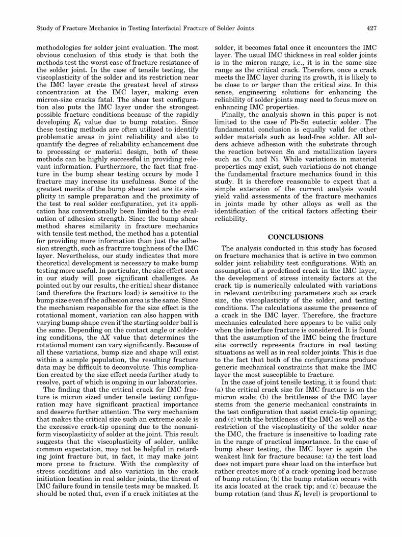
where R is the bump radius, and the negative signrepresents crack closing. In the diagram, C- is dis-placed by Du in the shear direction because visco-plastic flow at small shear distances is localized tothe bump/probe contact area and cannot affect thestrain field at the crack tip of the bump corner (inaddition, Du will be larger for larger bumps sincethe viscoplastic mass flow distance will be longer).Then, C+ + C- determines the net rate of crack-tip
opening with shear distance. As shown in the dia-gram, for large bumps, C+ is predominant in deter-mining the value of C+ + C-, making it increasemonotonically with shear distance. For small bumpsC+ is small enough to be affected by C-, and there-fore the total opening of the crack (C+ + C-) shows asinusoidal variation with shear distance (dottedline). Note the resemblance between the two cases ofC+ + C- with the K data for the 460 lm and 360 lmbumps shown in Fig. 11. It is therefore reasonableto conclude that the viscoplasticity of the soldercauses the bump to resist fracture, especially whenthe bump is small.
DISCUSSION
It is our belief that the analysis presented in thisinvestigation provides several insights that areuseful in enhanced utilization of the two testing
Fig. 12. Normalization of KIs in Fig. 11 by DX at various bump sizes.A relation between R and DX can also be seen in Table III .
Fig. 13. Schematic illustration of crack-tip opening by rotation, C+,and crack-tip closing by compressive deformation of solder bump, C-.In the C+ diagram, the thick solid line provides the value for a largesolder bump, while the thin solid line illustrates that for a small bump.This is also the case for the C- diagram. C+ + C-, which provides thenet crack-tip opening in degree, is displayed by the dashed (for largebump size) and dotted lines (for small bump size).
Bang, Moon, Kim, Kang, Jung, and Oh426
methodologies for solder joint evaluation. The mostobvious conclusion of this study is that both themethods test the worst case of fracture resistance ofthe solder joint. In the case of tensile testing, theviscoplasticity of the solder and its restriction nearthe IMC layer create the greatest level of stressconcentration at the IMC layer, making evenmicron-size cracks fatal. The shear test configura-tion also puts the IMC layer under the strongestpossible fracture conditions because of the rapidlydeveloping KI value due to bump rotation. Sincethese testing methods are often utilized to identifyproblematic areas in joint reliability and also toquantify the degree of reliability enhancement dueto processing or material design, both of thesemethods can be highly successful in providing rele-vant information. Furthermore, the fact that frac-ture in the bump shear testing occurs by mode Ifracture may increase its usefulness. Some of thegreatest merits of the bump shear test are its sim-plicity in sample preparation and the proximity ofthe test to real solder configuration, yet its appli-cation has conventionally been limited to the eval-uation of adhesion strength. Since the bump shearmethod shares similarity in fracture mechanicswith tensile test method, the method has a potentialfor providing more information than just the adhe-sion strength, such as fracture toughness of the IMClayer. Nevertheless, our study indicates that moretheoretical development is necessary to make bumptesting more useful. In particular, the size effect seenin our study will pose significant challenges. Aspointed out by our results, the critical shear distance(and therefore the fracture load) is sensitive to thebump size even if the adhesion area is the same. Sincethe mechanism responsible for the size effect is therotational moment, variation can also happen withvarying bump shape even if the starting solder ball isthe same. Depending on the contact angle or solder-ing conditions, the DX value that determines therotational moment can vary significantly. Because ofall these variations, bump size and shape will existwithin a sample population, the resulting fracturedata may be difficult to deconvolute. This complica-tion created by the size effect needs further study toresolve, part of which is ongoing in our laboratories.
The finding that the critical crack for IMC frac-ture is micron sized under tensile testing configu-ration may have significant practical importanceand deserve further attention. The very mechanismthat makes the critical size such an extreme scale isthe excessive crack-tip opening due to the nonuni-form viscoplasticity of solder at the joint. This resultsuggests that the viscoplasticity of solder, unlikecommon expectation, may not be helpful in retard-ing joint fracture but, in fact, it may make jointmore prone to fracture. With the complexity ofstress conditions and also variation in the crackinitiation location in real solder joints, the threat ofIMC failure found in tensile tests may be masked. Itshould be noted that, even if a crack initiates at the
solder, it becomes fatal once it encounters the IMClayer. The usual IMC thickness in real solder jointsis in the micron range, i.e., it is in the same sizerange as the critical crack. Therefore, once a crackmeets the IMC layer during its growth, it is likely tobe close to or larger than the critical size. In thissense, engineering solutions for enhancing thereliability of solder joints may need to focus more onenhancing IMC properties.
Finally, the analysis shown in this paper is notlimited to the case of Pb-Sn eutectic solder. Thefundamental conclusion is equally valid for othersolder materials such as lead-free solder. All sol-ders achieve adhesion with the substrate throughthe reaction between Sn and metallization layerssuch as Cu and Ni. While variations in materialproperties may exist, such variations do not changethe fundamental fracture mechanics found in thisstudy. It is therefore reasonable to expect that asimple extension of the current analysis wouldyield valid assessments of the fracture mechanicsin joints made by other alloys as well as theidentification of the critical factors affecting theirreliability.
CONCLUSIONS
The analysis conducted in this study has focusedon fracture mechanics that is active in two commonsolder joint reliability test configurations. With anassumption of a predefined crack in the IMC layer,the development of stress intensity factors at thecrack tip is numerically calculated with variationsin relevant contributing parameters such as cracksize, the viscoplasticity of the solder, and testingconditions. The calculations assume the presence ofa crack in the IMC layer. Therefore, the fracturemechanics calculated here appears to be valid onlywhen the interface fracture is considered. It is foundthat the assumption of the IMC being the fracturesite correctly represents fracture in real testingsituations as well as in real solder joints. This is dueto the fact that both of the configurations producegeneric mechanical constraints that make the IMClayer the most susceptible to fracture.
In the case of joint tensile testing, it is found that:(a) the critical crack size for IMC fracture is on themicron scale; (b) the brittleness of the IMC layerstems from the generic mechanical constraints inthe test configuration that assist crack-tip opening;and (c) with the brittleness of the IMC as well as therestriction of the viscoplasticity of the solder nearthe IMC, the fracture is insensitive to loading ratein the range of practical importance. In the case ofbump shear testing, the IMC layer is again theweakest link for fracture because: (a) the test loaddoes not impart pure shear load on the interface butrather creates more of a crack-opening load becauseof bump rotation; (b) the bump rotation occurs withits axis located at the crack tip; and (c) because thebump rotation (and thus KI level) is proportional to
Study of Fracture Mechanics in Testing Interfacial Fracture of Solder Joints 427
the rotational moment, the fracture is subjected tothe bump size effect.
ACKNOWLEDGEMENTS
The work at Seoul National University wassupported by Brain Korea 21, Korea. The work atthe University of Texas at Arlington was supportedby a grant from the Korea Research Foundation(KRF-2005-000-10442).
REFERENCES
1. A.J. Sunwoo, J.W. Morris, and G.K. Lucey, Metall. Trans. A23A, 1323 (1992).
2. B.J. Lee, N.M. Hwang, and H.M. Lee, Acta Mater. 45, 1867(1997).
3. R.J. Fields, R.R. Low, and G.K. Lucey, The Metal Science ofJoining, ed. M.J. Cieslak, M.E. Glicksman, S. Kang, andJ. Perepezko (Ohio: TMS, 1991), p. 165.
4. B. Balakrisnan, C.C. Chum, M. Li, Z. Chen, and T. Cahyadi,J. Electron. Mater. 32, 166 (2003).
5. L.K. Quan, D. Frear, D. Grivas, and J.W. Morris, J. Elec-tron. Mater. 16, 203 (1987).
6. R.J. Asaro, N.P. O�Dowd, and C.F. Shih, Mater. Sci. Eng.162A, 175 (1993).
7. H.-T. Lee and M.-H. Chen, Mater. Sci. Eng. A333, 24 (2002).
8. K.H. Prakash and T. Sritharan, Mater. Sci. Eng. 379, 277(2004).
9. L.K. Quan (MS Thesis, U.C. Berkeley, CA, 1988).10. JESD22-B117: BGA Bump Shear, Published by JEDEC
Solid State Technology Association (Virginia: JEDEC, 2000).11. G.J. Irwin, Appl. Mech. 24, 361 (1957).12. T.L. Anderson, Fracture Mechanics: Fundamentals and
Applications, 2nd ed. (London: CRC Press, 1994), pp. 29–96.13. J.-W. Kim and S.-B. Jung, Mater. Sci. Eng. A371, 267
(2004).14. X. Huang, S.-W.R. Lee, C.C. Yan, and S. Hui (Proceedings of
51st Electronic Components & Technology Conference,ECTC, Florida, 2001), p. 1065.
15. J. L. Marshall, The Mechanics of Solder Alloy Interconnects,ed. D.R. Frear, S.N. Burchett, H.S. Morgan, and J.H. Lau(New York: Van Nostraind Reinhold, 1994), p. 42.
16. E.W. Hare and R.G. Stang, J. Electron. Mater. 24, 1473(1995).
17. Hibbit, Karlson & Sorensen: ABAQUS/Standard User�sManual, Ver. 6.3 (2003), ch. 7.9.
18. ASTM E399-90: Standard Test Method for Plane StrainFracture Toughness of Metallic Materials (ASTM, Phila-delphia), (1990), E1290-02.
19. D.R. Frear and P.T. Vianco, Metall. Mat. Trans. 25A, 1509(1994).
20. D.B. Bogy, J. Appl. Mech. 38, 377 (1971).
Bang, Moon, Kim, Kang, Jung, and Oh428


![1 Interfacial Rheology System. 2 Background of Interfacial Rheology Interfacial Shear Stress Interfacial Shear Viscosity = [ ]](https://img.pdfslide.net/doc/110x75/56649d1f5503460f949f3d29/1-interfacial-rheology-system-2-background-of-interfacial-rheology-interfacial.jpg)