Embed Size (px)
Citation preview

7/27/2019 18 Anshul Shrivas ENT502 2012 DSD Assignment
http://slidepdf.com/reader/full/18-anshul-shrivas-ent502-2012-dsd-assignment 1/19
DIGITAL SYSTEM DESIGN AND SYNTHESIS (ENT-502)
ASSIGNMENT
1 SUBMITTED BY ANSHUL R. SHRIVAS
Roll no: 18
1ST
SEM M.Tech – VLSI DESIGN
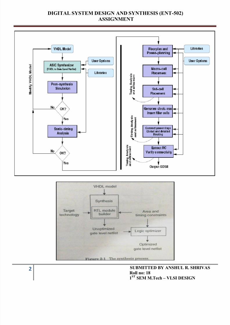
Ques.1. Explain the Stages of synthesis.
Ans:Synthesis means here that a VHDL description provided by the user is taken as the specification of the
hardware and mapped to either an IC or an FPGA layout that shows the same behavior as the specification. Onecan say that the synthesis tools perform silicon compilation. In a way similar to software compilation where thespecification of some computation in a high-level language such as C++ or Java is automatically translated into
machine instructions, a silicon compiler translates a high-level specification of hardware behavior into a set of
mask patterns on chip that realizes the desired behavior.The VHDL synthesis process can be seen as consisting of 1
stderiving Boolean equations from the
VHDL code and then optimizing these equations such that they can be realized with the standard cells from a
given library. After VHDL synthesis, the resulting netlist of standard cells can again be described in VHDL. It
will, of course, be a structural description where instances of standard cells are interconnected. Behavioraldescriptions of the individual standard cells themselves are given in the library. This final VHDL description of
the design can again be simulated using the original testbench. There are two reasons for simulating the final
description. First of all, the final description will contain timing information based on a realistic modeling ofdelays. It may turn out that the circuit does not work properly due to timing problems. They may be solved by a
revision of the design. A second reason for postsynthesis simulation is that the synthesis tools cannot always be
trusted; due to the complexity of the algorithms, bugs may exist in the software.
These are the main properties of the synthesizable subset of VHDL:
Only a single architecture for each entity to be synthesized is allowed. A second architecture presentedto the system will result in the 1st one to be ignored. Configurations do not make sense because no
confusion between multiple architectures is possible.
The architecture of an entity can either be a behavioral one or a structural one composed ofinstantiations of other entities. So, hierarchical descriptions can be used. Multiple entities per file areallowed.
Behavioral descriptions of an entity will have one or more processes in the architecture body. It is agood custom to separate combinational and sequential logic into separate processes. Examples are given
later on.
Synthesizable VHDL should not contain references to absolute time such as in assignments with the
after keyword. If they do, they are ignored. Signals can be delayed, but only by passing them through
clocked registers.
Although the synthesizer can deal with many data types, it is strongly recommended to exclusively usethe std logic and std logic vector data types for the I/O signals of the toplevel entities. These are namelythe data types used in the VHDL descriptions of the synthesized circuits. Sticking to them facilitates the
reuse of testbenches.
Stages of Synthesis:
Following are stages of synthesis:
Specify library search path and libraries
Set global constraints (clock period)
Set operating conditions and wire load model
Write output netlist, constraints and reports
7/27/2019 18 Anshul Shrivas ENT502 2012 DSD Assignment
http://slidepdf.com/reader/full/18-anshul-shrivas-ent502-2012-dsd-assignment 2/19
DIGITAL SYSTEM DESIGN AND SYNTHESIS (ENT-502)
ASSIGNMENT
2 SUBMITTED BY ANSHUL R. SHRIVAS
Roll no: 18
1ST
SEM M.Tech – VLSI DESIGN
7/27/2019 18 Anshul Shrivas ENT502 2012 DSD Assignment
http://slidepdf.com/reader/full/18-anshul-shrivas-ent502-2012-dsd-assignment 3/19
DIGITAL SYSTEM DESIGN AND SYNTHESIS (ENT-502)
ASSIGNMENT
3 SUBMITTED BY ANSHUL R. SHRIVAS
Roll no: 18
1ST
SEM M.Tech – VLSI DESIGN
Ques.2. Explain Synthesis constraints.
Ans:Synthesis constraints instruct the synthesis tool to perform specific operations. The following constraints
are synthesis constraints:
1) FROM-TO2) TIG3) TIMEGRP
4) TNM
5) TNM NET 6) OFFSET
Xilinx software enables you to specify precise timing constraints for your Xilinx designs. You can specify the
timing constraints for any nets or paths in your design, or you can specify them globally. One way of specifying
path requirements is to first identify a set of paths by identifying a group of start and end points. The start andend points can be flip flops, I/O pads, latches, or RAMs. You can then control the worst-case timing on the set
of paths by specifying a single delay requirement for all paths in the set. The primary way to specify timing
constraints is to enter them in your design (HDL and schematic). However, you can also specify timingconstraints in constraints files (UCF, NCF, PCF, XCF). Once you define timing specifications and map the
design, PAR places and routes your design based on these requirements.
AREA_GROUP BEL CONFIG a; a. when used with PROHIBIT
LOC LOCATE OPT_EFFORT PROHIBIT RLOC RLOC_ORIGIN
RLOC_RANGE USE_RLOC
FROM-TO IOB KEEP
MAP OFFSET PERIODTIG TNM TNM_NET
To analyze the results of timing specifications, use the command line tool, TRACE (TRCE) or the ISE tool
Timing Analyzer.XST Timing Constraints
XST supports XCF (XST Constraints File) syntax to define synthesis and timing constraints. The
constraint syntax in use prior to the ISE 7.1i release is no longer supported. Timing constraints supported by
XST can be applied via either:
The -glob_opt command line switch
Command Line Switch
Using the -glob_opt command line switch is the same as selecting Process Properties Synthesis
Options > Global Optimization Goal. Using this method allows you to apply global timing constraints to the
entire design. You cannot specify a value for these constraints; XST will optimize them for the best
performance. These constraints are overridden by constraints specified in the constraints file.
Constraints File
Using the constraint file method, you can use the native UCF timing constraint syntax. Using the XCF
syntax, XST supports constraints such as TNM_NET, TIMEGRP, PERIOD, TIG, FROM-TO, including
wildcards and hierarchical names.The following timing constraints are supported in the XST Constraints File (XCF).

7/27/2019 18 Anshul Shrivas ENT502 2012 DSD Assignment
http://slidepdf.com/reader/full/18-anshul-shrivas-ent502-2012-dsd-assignment 4/19
DIGITAL SYSTEM DESIGN AND SYNTHESIS (ENT-502)
ASSIGNMENT
4 SUBMITTED BY ANSHUL R. SHRIVAS
Roll no: 18
1ST
SEM M.Tech – VLSI DESIGN
FROM-TO
FROM-TO defines a timing constraint between two groups. A group can be user-defined or predefined
(FFS, PADS, RAMS).
Following is an example of XCF Syntax:
TIMESPEC “TSname
”=FROM “ group1
” TO “ group2
”value;
OFFSET
OFFSET is a basic timing constraint. It specifies the timing relationship between an external clock and
its associated data-in or data-out pin. pad-related signals, and cannot be used to extend the arrival time
specification method to the internal signals in a design.OFFSET allows you to:
1. Calculate whether a setup time is being violated at a flip-flop whose data and clock inputs are derived
from external nets.
2. Specify the delay of an external output net derived from the Q output of an internal flip-flop beingclocked from an external device pin.
For more information, see the “OFFSET” constraint.
XCF Syntax:OFFSET = {IN|OUT} “offset_time” [units] {BEFORE|AFTER } “clk_name”
[TIMEGRP “group_name”];
TIG
The “TIG” constraint causes all paths going through a specific net to be ignored for timing analyses and
optimization purposes. This constraint can be applied to the name of the signal affected. XCF Syntax:
NET “netname” TIG;
TIMEGRP
“TIMEGRP” is a basic grouping constraint. In addition to naming groups using the TNM identifier, youcan also define groups in terms of other groups. You can create a group that is a combination of existing groups
by defining a TIMEGRP constraint.
You can place TIMEGRP constraints in a constraints file (XCF or NCF). You can use TIMEGRP attributes tocreate groups using the following methods.
1. Combining multiple groups into one
2. Defining flip-flop subgroups by clock sense
XCF Syntax:
TIMEGRP “newgroup”=”existing_grp1” “existing_grp2”
[“existing_grp3” . . .];
TNM
“TNM” is a basic grouping constraint. Use TNM (Timing Name) to identify the elements that make up agroup, which you can then use in a timing specification. TNM tags specific FFS, RAMs, LATCHES, PADSBRAMS_PORTA, BRAMS_PORTB, CPUS, HSIOS, and MULTS as members of a group to simplify the
application of timing specifications to the group.
The RISING and FALLING keywords may also be used with TNMs.
XCF Syntax:{NET | PIN} “net_or_pin_name” TNM=[ predefined_group:] identifier ;

7/27/2019 18 Anshul Shrivas ENT502 2012 DSD Assignment
http://slidepdf.com/reader/full/18-anshul-shrivas-ent502-2012-dsd-assignment 5/19
DIGITAL SYSTEM DESIGN AND SYNTHESIS (ENT-502)
ASSIGNMENT
5 SUBMITTED BY ANSHUL R. SHRIVAS
Roll no: 18
1ST
SEM M.Tech – VLSI DESIGN
TNM Net
“TNM_NET” is essentially equivalent to TNM on a net except for input pad nets. Special rules apply
when using TNM_NET with the “PERIOD” constraint for DLL/DCMs in the following devices:
1. Virtex
2.
Virtex-E3. Virtex-II
4. Virtex-II Pro5. Virtex-II Pro X tifier ;
A TNM_NET is a property that you normally use in conjunction with an HDL design to tag a specific net. All
downstream synchronous elements and pads tagged with the TNM_NET identifier are considered a group.
Ques.3. Explain Logic partitioning.
Ans:The logic partition is determined by human designers. A good partition simplifies and streamlines the
development and verification process, and makes the code reliable and portable. To facilitate the synthesis, a
“logical circuit part” in the hierarchy should be within the range of the maximal gate count recommended by thesynthesis software. On the other hand, since synthesis software can flatten and collapse a part of the hierarchy,smaller “logical parts “can be used to design the hierarchy.
In addition to synthesis concerns, partition should also be used to develop reliable design and portable
reuse of the code. We should pay particular attention to the circuits that may hinder the portability or introduce
problem in the development flow. It is good idea to separate these circuits from the ordinary logic andinstantiate them as component in the design hierarchy. Two types of circuit of concerns are:
1) Device-dependent circuits
2) Non-Boolean circuits
1. Device-dependent circuitsDevice-dependent circuits are those not synthesized by generic logic gates. They are predesigned or
prefabricated for a specific device technology. For example, most device technology has various types of prefabricated memory modules. These circuits are inferred by component instantiation and require nosynthesis. Once the device-dependent circuit is used, the VHDL code becomes device-dependent. To
maintain the portability, one way is to isolate the circuits in the top-level hierarchy and instantiate them as
individual components. If VHDL is used later for a different device technology, we need only the substitute
these components with the equivalent circuits of the new technology and keep the remaining code intact.
2. Non-Boolean circuitsDigital system design is primarily based on a mathematical model of Boolean algebra and its derivative.
The algorithm in analysis, synthesis, verification and testing are developed within this framework. If thecircuit does not follow basic mathematical model, we call it a non-Boolean circuits. Some examples are
listed below
a. Tristate buffer: It has third possible value, high impedance, in its output. The high impedance cannot
be optimized or propagated as regular logic values.
b. Delay-sensitive circuits: It uses logic gates to introduce a specific amount of propagation delay. The
function of the circuit relies on the delay characteristics, not on Boolean algebra manipulation.
c. Clock distribution circuits: It distributes the clock signal to the connected FFs. The circuit functions
as a current amplifier and performs no logic operation.
d. Synchronization circuits: It uses FFs to resolve the metastable condition, not for regular storage.

7/27/2019 18 Anshul Shrivas ENT502 2012 DSD Assignment
http://slidepdf.com/reader/full/18-anshul-shrivas-ent502-2012-dsd-assignment 6/19
DIGITAL SYSTEM DESIGN AND SYNTHESIS (ENT-502)
ASSIGNMENT
6 SUBMITTED BY ANSHUL R. SHRIVAS
Roll no: 18
1ST
SEM M.Tech – VLSI DESIGN
Ques.4. Explain Logic described by RTL
Ans:Register Transfer Level, or RTL1 design lies between a purely behavioral description of the desired
circuit and a purely structural one. An RTL description describes a circuit’s registers and the sequence of
transfers between these registers but does not describe the hardware used to carry out these operations.The steps in RTL design are: (1) determine the number and sizes of registers needed to hold the data used by thedevice, (2) determine the logic and arithmetic operations that need to be performed on these register contents,
and (3) design a state ma- chine whose outputs control how the register contents are updated in order to obtain
the desired results. Producing an RTL design is similar to writing a computer program in a conventional programming language. Choosing registers is the same as choosing variables.
Designing the flow of data in the “datapath” is analogous to writing expressions involving the variables
(registers) and operators (combinational functions). Designing the controller state machine is similar to deciding
on the flow of control within the program (if/then/else, while-loops, etc). As a simple example, consider adevice that needs to add four numbers. In VHDL, given signals of the correct type, we can simply write:
s <= a + b + c + d ;
This particular description is simple enough that it can be synthesized. A behavioral description, not beingconcerned with implementation details, would be complete at this point. However, if we were concerned about
the cost of the implementation we might decide to break down the computation into a sequence of steps, each
one involving only a single addition:
s=0s=s+a
s=s+b
s=s+cs=s+d
where each operation is executed sequentially. The logic required is now one adder, a register to hold the value
of s in-between operations, a multiplexer to select the input to be added, and a circuit to clear s at the start of the
computation. Although this approach only needs one adder, the process requires more steps and will takelonger. Circuits that divide up a computation into a sequence of arithmetic and logic operations are quite
common and this type of design is called Register Transfer Level (RTL) or “data flow” design.
An RTL design is composed of (1) registers and combinational function blocks (e.g. adders andmultiplexers) called the data path and (2) a finite state machine, called the controller that controls the transfer of
data through the function blocks and between the registers. In VHDL RTL design the gate-level design and
optimization of the data path (registers, multiplexers, and combinational functions) is done by the synthesizer.
However, the designer must design the state machine and decide which register transfers are per formed inwhich state.
The RTL designer can trade off datapath complexity (e.g. using more adders and thus using more chip
area) against speed (e.g. having more adders means fewer steps are required to obtain the result). RTL design is
well suited for the design of CPUs and special-purpose processors such as disk drive controllers, video displaycards, network adapter cards, etc. It gives the designer great flexibility in choosing between processing speed
and circuit complexity.
The diagram below shows a generic component in the data path. Each RTL design will be composed ofone of the following building blocks for each register. The structure allows the contents of each register to be
updated at the end of each clock period with a value selected by the controller. The widths of the registers, the

7/27/2019 18 Anshul Shrivas ENT502 2012 DSD Assignment
http://slidepdf.com/reader/full/18-anshul-shrivas-ent502-2012-dsd-assignment 7/19
DIGITAL SYSTEM DESIGN AND SYNTHESIS (ENT-502)
ASSIGNMENT
7 SUBMITTED BY ANSHUL R. SHRIVAS
Roll no: 18
1ST
SEM M.Tech – VLSI DESIGN
types of combinational functions and their inputs will be determined by the application. A typical design willinclude many of these components.
RTL Timing Analysis:
As usual, the data path should be designed as a synchronous sequential circuit that uses the same clock
for all registers. All register contents thus change at the same time. The controller also uses the same clock as
the data path. The result is that each data path register loads the values “computed” during one state at the endof that state (which is then the start of the computation for the next state).We can guarantee that the correct
results will be loaded into registers if the longest propagation delay (t PD) through any path through the
combinational logic that lies between register outputs and inputs is less than the clock period (t clock) minus theregisters’ setup time (ts) and clock -to-output (t CO) delays:
7/27/2019 18 Anshul Shrivas ENT502 2012 DSD Assignment
http://slidepdf.com/reader/full/18-anshul-shrivas-ent502-2012-dsd-assignment 8/19
DIGITAL SYSTEM DESIGN AND SYNTHESIS (ENT-502)
ASSIGNMENT
8 SUBMITTED BY ANSHUL R. SHRIVAS
Roll no: 18
1ST
SEM M.Tech – VLSI DESIGN
Using a single clock means we only need to compute the delay through combinational logic blockswhich is much simpler than having to predict the effect of propagation delays on clock signals. This is why
almost all large-scale digital circuits are synchronous designs. Synthesis tools can be asked to synthesize logic
that operates at a particular clock period. The synthesizer is supplied with the propagation delay specificationsfor the combinational logic components available in the particular technology being used and it will then try to
arrange the logic so that the longest propagation delay between any register output and any register input is less
than the clock period (minus setup and clock-to-output delays). This ensures that the circuit will work properlyat the specified clock rate.
Ques 5. Explain static timing analysis.
Ans:You can perform timing analysis at several stages in the implementation flow to show your design
delays. You create or generate the following:1. A post-map timing report to evaluate the effects of logic delays on timing constraints.
2. A post-place-and-route timing report that incorporates both block and routing delays as a final analysis
of the design’s timing constraints The Interactive Timing Analyzer tool produces detailed timing constraint, clock, and path analysis for post-map
or post-place-and-route implementations.
Static Timing Analysis after Map
Post-map timing reports can be very useful in evaluating timing performance. Although route delays are
not accounted for, the logic delays can provide valuable information about the design. If logic delays accountfor a significant portion (> 50%) of the total allowable delay of a path, the path may not be able to meet your
timing requirements when routing delays are added.
Routing Delays
Routing delays typically account for 45% to 65% of the total path delays. By identifying problem paths
you can mitigate potential problems before investing time in place and route. You can:1. Redesign the logic paths to use fewer levels of logic.
2. Tag the paths for specialized routing resources.
3. Move to a faster device.4. Allocate more time for the path.
Logic-Only Delays
If logic-only delays account for much less (<35%) than the total allowable delay for a path or timing
constraint, the place-and-route software can use very low placement effort levels. In these cases, reducing effort
levels allows you to decrease runtimes while still meeting performance requirements.
Static Timing Analysis after Place and Route
Post-PAR timing reports incorporate all delays to provide a comprehensive timing Summary. If a placedand routed design has met all of your timing constraints, you can proceed by creating configuration data and
downloading a device.
Synchronous Timing Report
If you identify problems in the timing reports, you can:1. Increase the placer effort level.

7/27/2019 18 Anshul Shrivas ENT502 2012 DSD Assignment
http://slidepdf.com/reader/full/18-anshul-shrivas-ent502-2012-dsd-assignment 9/19
DIGITAL SYSTEM DESIGN AND SYNTHESIS (ENT-502)
ASSIGNMENT
9 SUBMITTED BY ANSHUL R. SHRIVAS
Roll no: 18
1ST
SEM M.Tech – VLSI DESIGN
2. Use re-entrant routing.3. Use multi-pass place and route.
You can also:
1. Redesign the logic paths to use fewer levels of logic.2. Tag the paths for specialized routing resources.
3. Move to a faster device.
4. Allocate more time for the paths.
Detailed Timing Analysis
To perform detailed timing analysis:
1. Open Project Navigator.
2. Select your project in the Sources window.
3. Double click Timing Analyzer under Launch Tools in the Processes window.This allows you to:
1. Specify specific paths for analysis.
2. Discover paths not affected by timing constraints.
3. Analyze the timing performance of the implementation based on another speed grade.
Ques.6. Explain Synchronous FSM Design.
Ans:All introduced digital circuits and systems have been described at the "Register Transfer Level" (RTL):
Signals are stored in registers and combinational logic blocks are located between the registers. All flip-flops of a synchronous system are clocked with one common triggering waveform CLK.
External asynchronous reset and preset signals should be synchronised in order to avoid coincidence with
the clock signal’s transitions. All other flip-flop resets or presets are controlled synchronously (i. e. by a FSM controller). Digital systems
designed by these criteria will work stable without oscillating effects and won't be influenced seriously by
any hazards: Manufacturers will guarantee flip-flop without hazards in output transitions.
All glitches which are caused by race glitches during state transitions and static hazards in output logic can be assumed to have duration less than the clock period.
Up to this chapter the main concern and emphasis was concentrated on functional design and analysisissues: so called "front end" of digital system development.
Several timing considerations and problem areas were purposely avoided:
1. The designer has to insure that no shift in the triggering clock edge of one flip-flop relative to another
will exist (clock skew) which can cause erroneous transitions.

7/27/2019 18 Anshul Shrivas ENT502 2012 DSD Assignment
http://slidepdf.com/reader/full/18-anshul-shrivas-ent502-2012-dsd-assignment 10/19
DIGITAL SYSTEM DESIGN AND SYNTHESIS (ENT-502)
ASSIGNMENT
10 SUBMITTED BY ANSHUL R. SHRIVAS
Roll no: 18
1ST
SEM M.Tech – VLSI DESIGN
2. All setup tSU and hold time tH requirements (sampling intervall tSU + tH) have to be meet especiallyunder clock skew influence.
3. External asynchronous input signals have to be synchronised with input flip-flops in order to prevent
metastable flip-flop states within the digital system. Metastable states of synchronizers have to be prevented either. Several of these activities belong to the "back end" design after having performed the
RTL development.
Timing Considerations in Synchronous Systems with a Data and Control Path
A digital system can be partitioned into the control logic section and the data path section: processormodule.
• The control logic section consists of all the FSM logic required to generate control signals for the data path
section. It receives status signals from the data path section.
• The data path section consists of all the logic used to store and transform data.
Timing example of a coupled control and data path
1. Shortly after the first positive clock edge the FSM controller has a transition to new valid state. The data path status signal registers concurrently deliver new values with a D flip-flop delay. (at 360 ns)
2. FSM Moore outputs are updated after a delay by the output forming logic. These control signals will
influence the data path behaviour with the next clock edge (at 380 ns).
3.
The calculation results of the data path are updated at 400 ns.4. The next state forming logic of the FSM controller delivers new values at 430 ns. It is more convenient
to assume that in most cases data path logic will cause larger delays.

7/27/2019 18 Anshul Shrivas ENT502 2012 DSD Assignment
http://slidepdf.com/reader/full/18-anshul-shrivas-ent502-2012-dsd-assignment 11/19
DIGITAL SYSTEM DESIGN AND SYNTHESIS (ENT-502)
ASSIGNMENT
11 SUBMITTED BY ANSHUL R. SHRIVAS
Roll no: 18
1ST
SEM M.Tech – VLSI DESIGN
Ques 7. Explain timing budgeting
Ans: Over past decades, academia and industry have invested much effort in computer- aided-design research
related to physical designs, including floor planning, partitioning, placement, and routing .By integrating
various techniques, many design methods and software systems have been developed for chip designs. One ofthe most popular design methods uses schematics as the design entry, follows by floor planning, placement, androuting to produce final chip layouts. This design method is very effective and efficient on small to medium-
scaled designs. However, with the advent of deep-submicron technology, the complexity of chip designs has
increased considerably in the past few years. Using a logic-level specification as the design entry may not beadequate to handling designs of such complexities. Consequently, more and more designers move their design
entry to a higher abstraction, e.g., RTL, instead of logic level. Furthermore, as devices' geometries shrink, chip
designers are facing a new set of design challenges, especially in electrical characteristics of circuits Figure 1
shows a typical RTL-based design flow consisting of two stages: (1) RTL/logic-level synthesis and (2) physical- level synthesis. In the first stage, the designer applies an RTL/logic-level synthesis procedure to
convert the RTL design specification into a gate-level design.
1. RTL/logic-level synthesisUsing such an RTL-based design flow, one of the crucial design considerations is the timing closure
issue. Consider that an RTL-based design flow involves multi-level design tasks, including RTL/logic synthesis
floor planning, placement, and routing. At each design level, the designer needs to determine the delay budget
(i.e., the timing constraint) for the design. The ultimate goal is to achieve a timing-closure solution such that the
final layout design satisfies the timing requirement. It's crucial to provide proper delay budgets to the designthroughout the design process so that the design team can achieve the most cost-efficient chip layout while
satisfying the timing requirement. If the delay budget is over-constrained, the cost may overrun. On the other
hand, if the delay budget is under-constrained, the final chip layout may not meet the design requirement.Without physical information, determining delay budget for a design at RTL is a non-trivial problem. It is also a
very risky task because an inferior delay budget assignment may result in an infeasible design. One way to
solve this problem is to close the synthesis and physical design loop by exploiting the interaction between thesetwo design stages, as Loop A shown in Figure 1. This motivates us to develop an RTL delay-budgeting method
and a timing-closure-driven design flow.
7/27/2019 18 Anshul Shrivas ENT502 2012 DSD Assignment
http://slidepdf.com/reader/full/18-anshul-shrivas-ent502-2012-dsd-assignment 12/19
DIGITAL SYSTEM DESIGN AND SYNTHESIS (ENT-502)
ASSIGNMENT
12 SUBMITTED BY ANSHUL R. SHRIVAS
Roll no: 18
1ST
SEM M.Tech – VLSI DESIGN
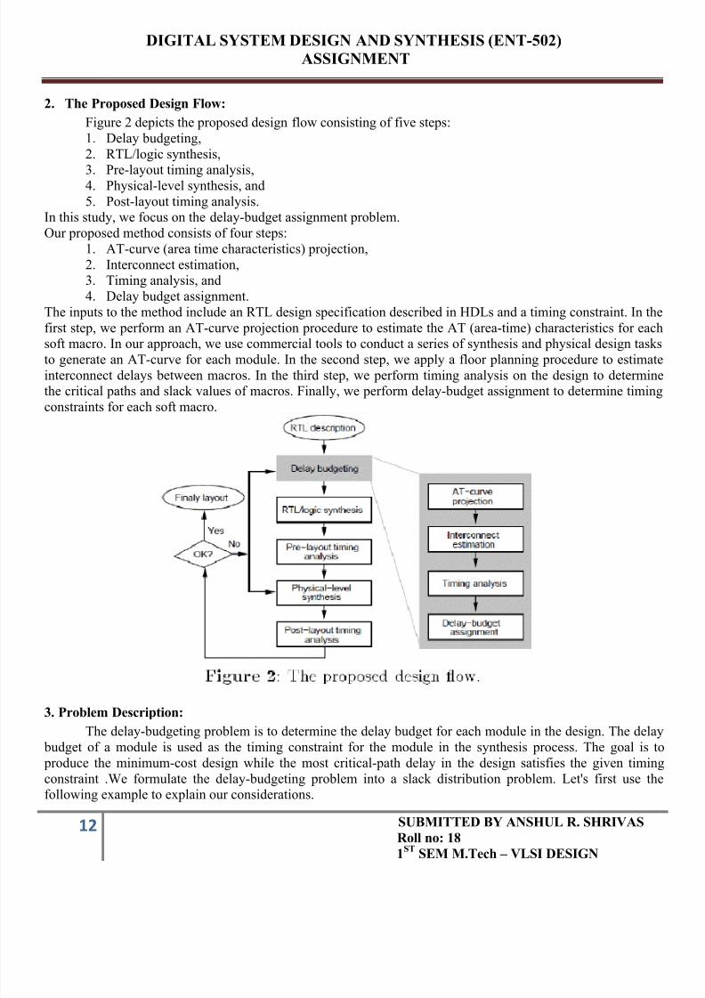
2. The Proposed Design Flow:
Figure 2 depicts the proposed design flow consisting of five steps:
1. Delay budgeting,
2. RTL/logic synthesis,
3.
Pre-layout timing analysis,4. Physical-level synthesis, and
5. Post-layout timing analysis.In this study, we focus on the delay-budget assignment problem.
Our proposed method consists of four steps:
1. AT-curve (area time characteristics) projection,
2. Interconnect estimation,3. Timing analysis, and
4. Delay budget assignment.
The inputs to the method include an RTL design specification described in HDLs and a timing constraint. In the
first step, we perform an AT-curve projection procedure to estimate the AT (area-time) characteristics for each
soft macro. In our approach, we use commercial tools to conduct a series of synthesis and physical design tasksto generate an AT-curve for each module. In the second step, we apply a floor planning procedure to estimate
interconnect delays between macros. In the third step, we perform timing analysis on the design to determinethe critical paths and slack values of macros. Finally, we perform delay-budget assignment to determine timing
constraints for each soft macro.
3. Problem Description:
The delay-budgeting problem is to determine the delay budget for each module in the design. The delay
budget of a module is used as the timing constraint for the module in the synthesis process. The goal is to
produce the minimum-cost design while the most critical-path delay in the design satisfies the given timing
constraint .We formulate the delay-budgeting problem into a slack distribution problem. Let's first use thefollowing example to explain our considerations.

7/27/2019 18 Anshul Shrivas ENT502 2012 DSD Assignment
http://slidepdf.com/reader/full/18-anshul-shrivas-ent502-2012-dsd-assignment 13/19
DIGITAL SYSTEM DESIGN AND SYNTHESIS (ENT-502)
ASSIGNMENT
13 SUBMITTED BY ANSHUL R. SHRIVAS
Roll no: 18
1ST
SEM M.Tech – VLSI DESIGN
As shown in Figure 4, there are p1..pq signal paths traveling from IN to OUT via modules m1 to m2There are two main considerations when we determine the delay budgets for the two modules. The first one is
the inter-module wire delay (dw) between the two modules. In today's deep-submicron technology, especially
when the modules become larger, the inter-module wire delay may become the dominant factor to the mostcritical-path delay. Hence, it's necessary to take the inter-module wire delay into consideration in the delay-
budgeting process .The second one is how to assign a cost-efficient delay budget to each module.
As we mentioned earlier, the delay budget assigned to each module will be used as the timing constraintwhen we synthesize the module into a gate-level design. Hence, the AT (area-time) characteristics of modules
may directly a_ect the _nal synthesized results when assigning different delay budgets to the modules. For
example, assume that we have a uniform AT characteristic for all paths from all inputs to all outputs inmodulem1 as well as in modulem2.
We also assume that m2 has a much steeper AT characteristic compared to that of m1, which means that
tightening the delay budget of m2 will result in a large increase in area cost. In this case, we prefer to assign arelaxing delay budget to m2 and a tightened delay budget to m1 in order to achieve a more cost-efficient
synthesized result. This motivates us to investigate the effect of taking into account AT characteristics of
modules in the delay-budgeting process.
Ques.8. Explain Modeling of FSM.Ans:
1. Moore FSM:
In a Moore FSM, the output of the circuit is dependent only on the state of the machine and not on its
inputs. This is shown in figure below:
Since the output dependent only on the state, a good way to describe a Moore machine is to use a
process statement with a case statement. The case statement is used to switch between the various states and the
output logic for each state is described in the appropriate branch. Either an if statement with a clock expressioncan be used around the case statement or a wait statement that triggers on every clock edge can be used as the
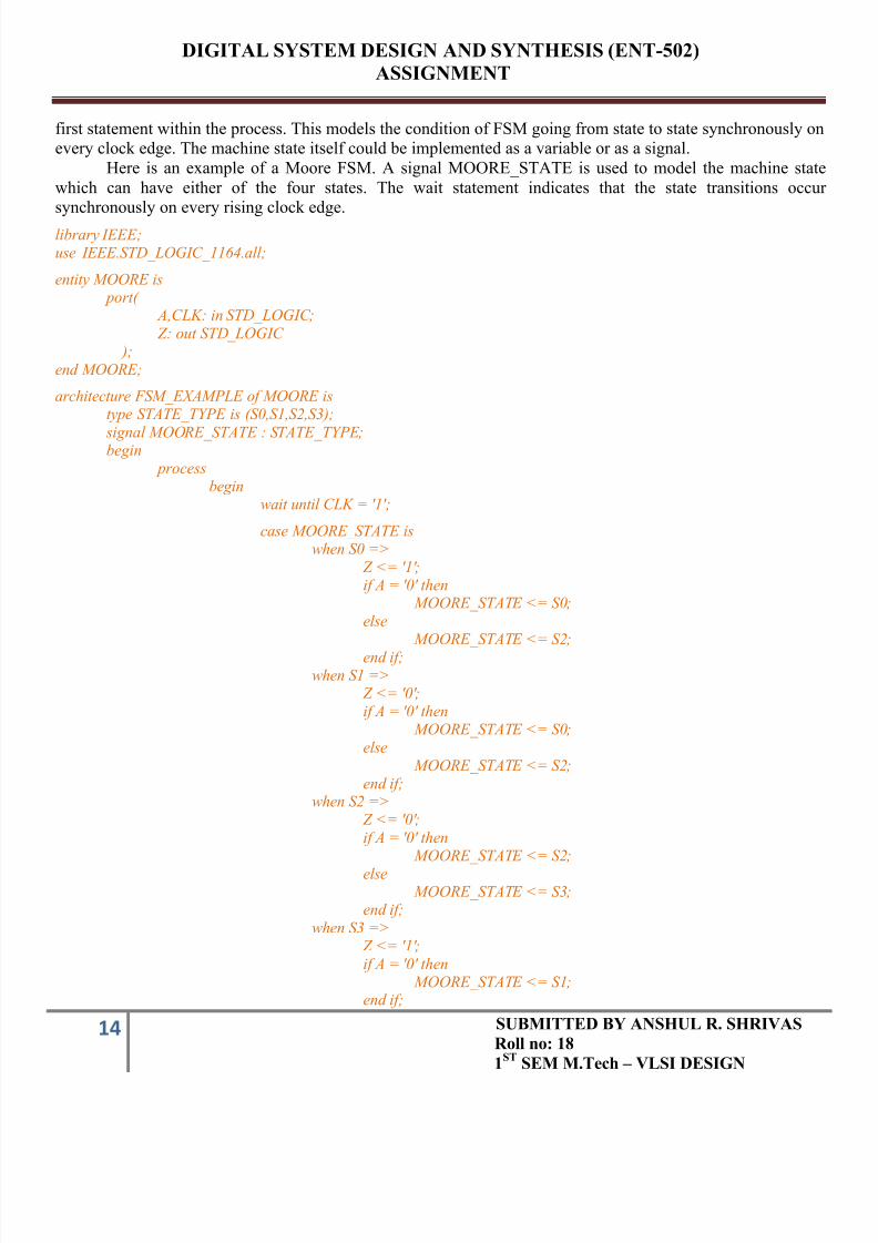
7/27/2019 18 Anshul Shrivas ENT502 2012 DSD Assignment
http://slidepdf.com/reader/full/18-anshul-shrivas-ent502-2012-dsd-assignment 14/19
DIGITAL SYSTEM DESIGN AND SYNTHESIS (ENT-502)
ASSIGNMENT
14 SUBMITTED BY ANSHUL R. SHRIVAS
Roll no: 18
1ST
SEM M.Tech – VLSI DESIGN
first statement within the process. This models the condition of FSM going from state to state synchronously onevery clock edge. The machine state itself could be implemented as a variable or as a signal.
Here is an example of a Moore FSM. A signal MOORE_STATE is used to model the machine state
which can have either of the four states. The wait statement indicates that the state transitions occursynchronously on every rising clock edge.
library IEEE;use IEEE.STD_LOGIC_1164.all;
entity MOORE is port(
A,CLK: in STD_LOGIC;
Z: out STD_LOGIC );
end MOORE;
architecture FSM_EXAMPLE of MOORE istype STATE_TYPE is (S0,S1,S2,S3);
signal MOORE_STATE : STATE_TYPE;begin
processbegin
wait until CLK = '1';
case MOORE_STATE iswhen S0 =>
Z <= '1';if A = '0' then
MOORE_STATE <= S0;
else MOORE_STATE <= S2;
end if;when S1 =>
Z <= '0';if A = '0' then
MOORE_STATE <= S0;
else MOORE_STATE <= S2;
end if;when S2 =>
Z <= '0';
if A = '0' then MOORE_STATE <= S2;
else MOORE_STATE <= S3;
end if;
when S3 => Z <= '1';
if A = '0' then MOORE_STATE <= S1;
end if;
7/27/2019 18 Anshul Shrivas ENT502 2012 DSD Assignment
http://slidepdf.com/reader/full/18-anshul-shrivas-ent502-2012-dsd-assignment 15/19
DIGITAL SYSTEM DESIGN AND SYNTHESIS (ENT-502)
ASSIGNMENT
15 SUBMITTED BY ANSHUL R. SHRIVAS
Roll no: 18
1ST
SEM M.Tech – VLSI DESIGN
end case;end process;
end FSM_EXAMPLE;
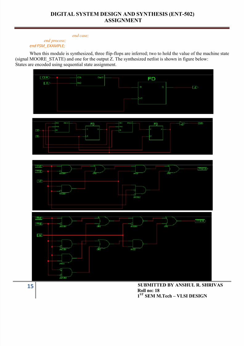
When this module is synthesized, three flip-flops are inferred; two to hold the value of the machine state
(signal MOORE_STATE) and one for the output Z. The synthesized netlist is shown in figure below:States are encoded using sequential state assignment.
7/27/2019 18 Anshul Shrivas ENT502 2012 DSD Assignment
http://slidepdf.com/reader/full/18-anshul-shrivas-ent502-2012-dsd-assignment 16/19
DIGITAL SYSTEM DESIGN AND SYNTHESIS (ENT-502)
ASSIGNMENT
16 SUBMITTED BY ANSHUL R. SHRIVAS
Roll no: 18
1ST
SEM M.Tech – VLSI DESIGN
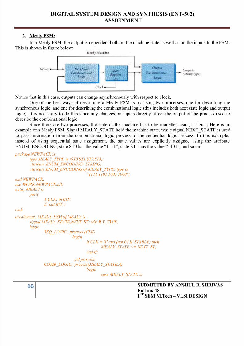
2. Mealy FSM:
In a Mealy FSM, the output is dependent both on the machine state as well as on the inputs to the FSM.
This is shown in figure below:
Notice that in this case, outputs can change asynchronously with respect to clock.One of the best ways of describing a Mealy FSM is by using two processes, one for describing the
synchronous logic, and one for describing the combinational logic (this includes both next state logic and output
logic). It is necessary to do this since any changes on inputs directly affect the output of the process used to
describe the combinational logic.Since there are two processes, the state of the machine has to be modelled using a signal. Here is an
example of a Mealy FSM. Signal MEALY_STATE hold the machine state, while signal NEXT_STATE is used
to pass information from the combinational logic process to the sequential logic process. In this example,instead of using sequential state assignment, the state values are explicitly assigned using the attribute
ENUM_ENCODING; state ST0 has the value “1111”, state ST1 has the value “1101”, and so on.
package NEWPACK is
type MEALY_TYPE is (ST0,ST1,ST2,ST3);attribute ENUM_ENCODING: STRING;
attribute ENUM_ENCODING of MEALY_TYPE: type is"1111 1101 1001 1000";
end NEWPACK;
use WORK.NEWPACK.all;entity MEALY is
port( A,CLK: in BIT; Z: out BIT);
end;
architecture MEALY_FSM of MEALY is
signal MEALY_STATE,NEXT_ST: MEALY_TYPE;begin
SEQ_LOGIC: process (CLK)begin
if CLK = '1' and (not CLK' STABLE) then MEALY_STATE <= NEXT_ST;
end if;
end process;COMB_LOGIC: process(MEALY_STATE,A)
begin
case MEALY_STATE is

7/27/2019 18 Anshul Shrivas ENT502 2012 DSD Assignment
http://slidepdf.com/reader/full/18-anshul-shrivas-ent502-2012-dsd-assignment 17/19
DIGITAL SYSTEM DESIGN AND SYNTHESIS (ENT-502)
ASSIGNMENT
17 SUBMITTED BY ANSHUL R. SHRIVAS
Roll no: 18
1ST
SEM M.Tech – VLSI DESIGN
when ST0 =>if A ='1' then
Z <= '1'; NEXT_ST <= ST3;
else Z <= '0';
NEXT_ST <= ST0;end if;
when ST1 =>if A ='1' then
Z <= '1'; NEXT_ST <= ST1;
else Z <= '0';
NEXT_ST <= ST0;end if;
when ST2 =>
if A ='0' then Z <= '0';
NEXT_ST <= ST2;else Z <= '1';
NEXT_ST <= ST1;end if;
when ST3 =>
if A ='0' then Z <= '0';
NEXT_ST <= ST2;else Z <= '1';
NEXT_ST <= ST1;end if;
end case;
end process;end MEALY_FSM;
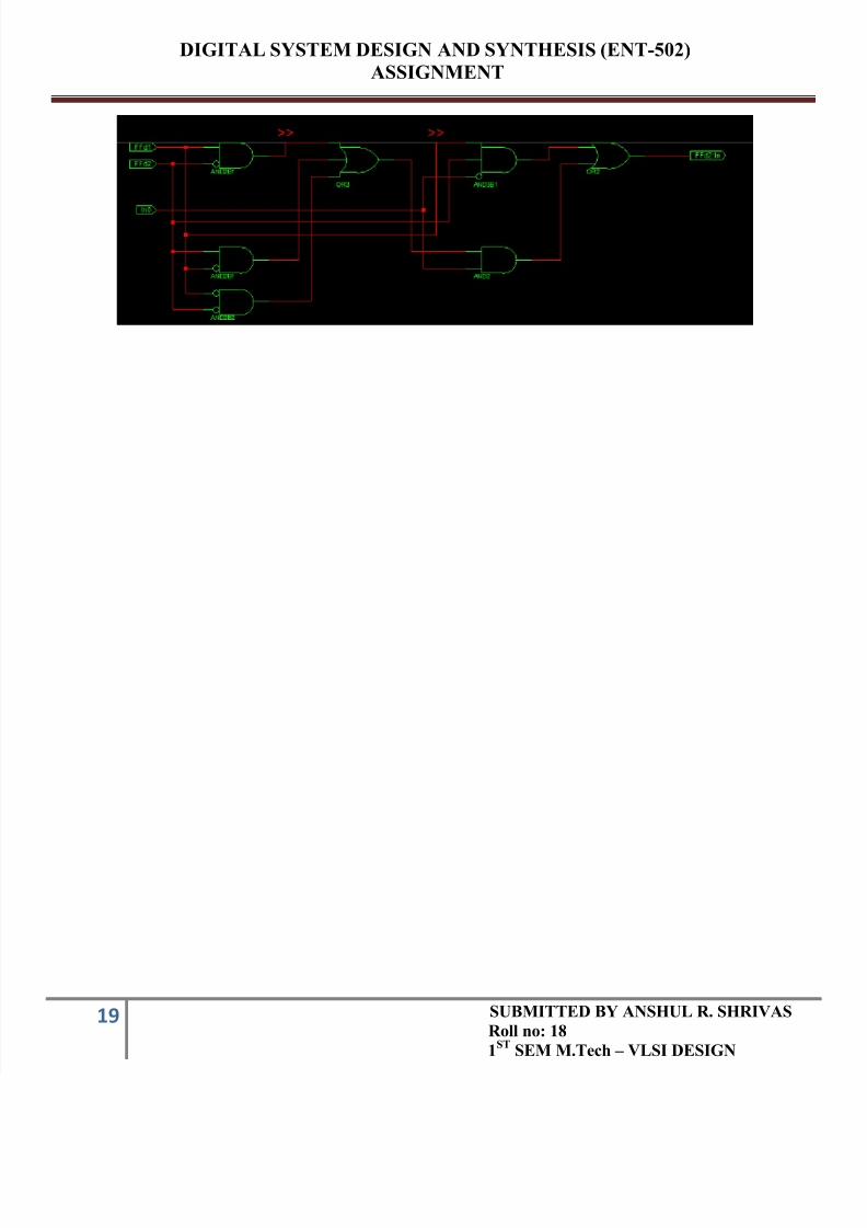
The synthesis netlist is shown below:

7/27/2019 18 Anshul Shrivas ENT502 2012 DSD Assignment
http://slidepdf.com/reader/full/18-anshul-shrivas-ent502-2012-dsd-assignment 18/19
DIGITAL SYSTEM DESIGN AND SYNTHESIS (ENT-502)
ASSIGNMENT
18 SUBMITTED BY ANSHUL R. SHRIVAS
Roll no: 18
1ST
SEM M.Tech – VLSI DESIGN
7/27/2019 18 Anshul Shrivas ENT502 2012 DSD Assignment
http://slidepdf.com/reader/full/18-anshul-shrivas-ent502-2012-dsd-assignment 19/19
DIGITAL SYSTEM DESIGN AND SYNTHESIS (ENT-502)
ASSIGNMENT
19 SUBMITTED BY ANSHUL R. SHRIVAS
Roll no: 18
1ST
SEM M Tech – VLSI DESIGN