Embed Size (px)
Citation preview

(19) United States US 2011 0140246A1
(12) Patent Application Publication (10) Pub. No.: US 2011/0140246A1 Hoenk et al. (43) Pub. Date: Jun. 16, 2011
(54) DELTA-DOPING AT WAFER LEVEL FOR HIGH THROUGHPUT, HIGHYIELD FABRICATION OF SILICON MAGING ARRAYS
Michael E. Hoenk, Valencia, CA (US); Shouleh Nikzad, Valencia, CA (US); Todd J. Jones, Altadena, CA (US); Frank Greer, Pasadena, CA (US); Alexander G. Carver, North Hollywood, CA (US)
(75) Inventors:
(73) Assignee: California Institute of Technology, Pasadena, CA (US) 12/965,790
Dec. 10, 2010
(21) Appl. No.:
(22) Filed: Related U.S. Application Data
(60) Provisional application No. 61/285,288, filed on Dec. 10, 2009, provisional application No. 61/303,551, filed on Feb. 11, 2010.
Thinned imager Wafer Carlorsica
listeside
Eurseseckc.cstays
Cassie Coasts sis
Srirate side
Sicia&striciisayer
Publication Classification
(51) Int. Cl. HOIL 29/66 (2006.01) HOIL 2L/30 (2006.01) C23C I6/02 (2006.01)
(52) U.S. Cl. ..................... 257/655; 438/471; 118/723 R: 257/E29,166; 257/E21.211
(57) ABSTRACT
Systems and methods for producing high quantum efficiency silicon devices. A silicon MBE has a preparation chamber that provides for cleaning silicon Surfaces using an oxygen plasma to remove impurities and a gaseous (dry) NH+NF room temperature oxide removal process that leaves the sili con Surface hydrogen terminated. Silicon wafers up to 8 inches in diameter have devices that can be fabricated using the cleaning procedures and MBE processing, including delta doping.
Oxygen plasma clean NH, -NF. Theroia Cherrica: Cear
iii.aixi-sites
63ried Eectronics:.ase:
artacts side
Automated, rapid, multiple wafer processes integrated into a single vacuum chamber
Patent Application Publication Jun. 16, 2011 Sheet 1 of 19 US 2011/O140246 A1
Trapping of photo-generated charge Back surface Front surface
Backside potential well Buried channel
FIG. 1
16 t
Delta-doped 15- MBE an
1,4- arra Ultrashallow implant d 1.3 lon implant m
8 Diffusion 2 1.2
1.1 L/ 1.0
0.9 - - -----|--|--|--|--|--|- O 5 1O 15 20 25 30
Depth from Surface (nm)
FIG 2

Patent Application Publication Jun. 16, 2011 Sheet 2 of 19 US 2011/O140246 A1
= 2.0
0.4 Delta-doped layer
18 O2
es
O.O. oe - - - - - - - - - - - - - - - x - - - - - / . . . . No ea A - - - - -v- - - - - - - - -v- a As a 2 1.6 g.
"Ground state" of quasi-bound electron -0.2 - (E = 1.63 eV) Se
2 S. - 14 S c -0.4
e s
s -0.6 - Backside Conduction band with
rir potential cirr continuum of unbound electronic states - 1.2 e -08 - k".-->
-10 1.O O 2 4 6 8 10
Depth from surface (nm)
FIG. 3
: popos a s a 2 &A
A Model, bilayer coating (65nm SiN., 93mm SiO) O Delta-doped CCD, AR-coated region
ri 8 × 8 Y & & & u v u & & & - - - X & A Delta-doped CCD, uncoated region X
- - - Silicon transmittance
300 400 500 600 700 800 900 1 OOO
Wavelength (nm)
FIG. 4

Patent Application Publication Jun. 16, 2011 Sheet 3 of 19 US 2011/O140246 A1
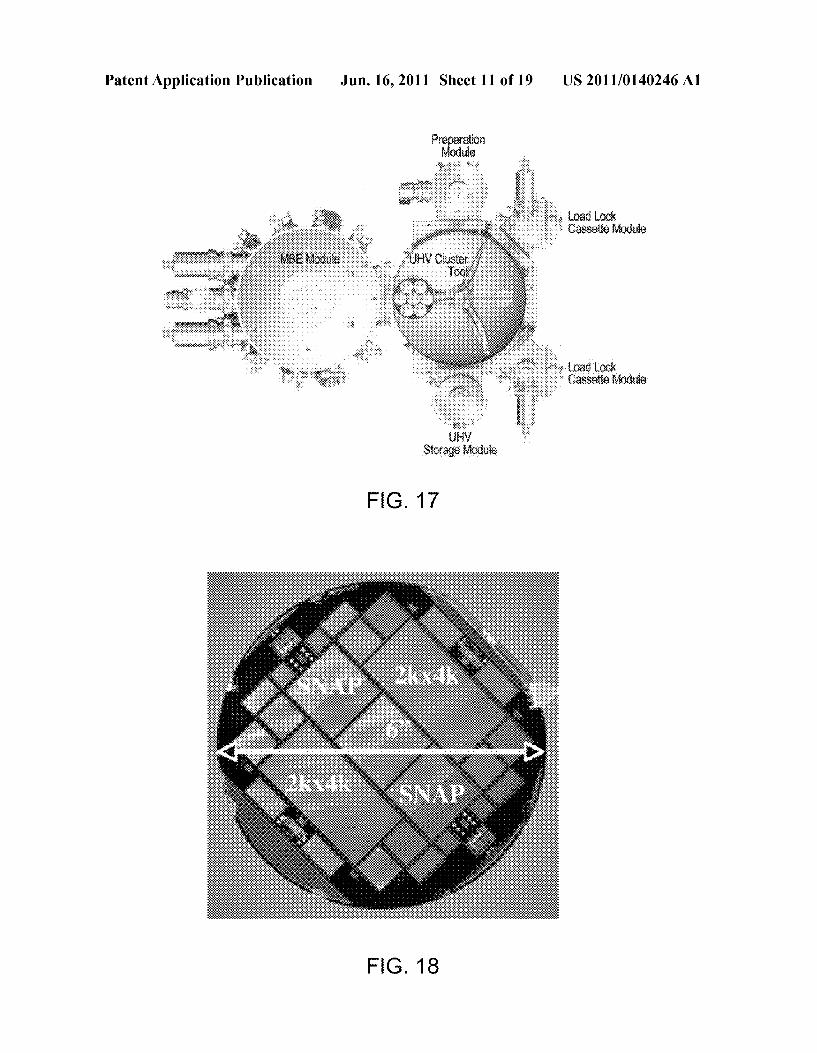
100 A 7 AR-coated
80 8-doped CCD s
5 60 É A Ay 8-doped CCD I A w
E
S AXA Unmodified Cy CCD
20 A N
WF/PCII O
100 300 500 700 Wavelength (nm)
FIG. 5
100
8 O & & & Back illumin ated
6 O
4 O & v & & Front illuminated cri
400 500 600 700 800 900 1000 1100
Wavelength (nm)
F.G. 6
Patent Application Publication Jun. 16, 2011 Sheet 4 of 19 US 2011/O140246 A1
100
& & 80 -
i 60 - s
40 Sitransmittance
s 88: I. After 6-doping g 20 A 18 mos. later C to 3 Vrs later
O 300 400 500 600
Wavelength (nm)
FIG. 7
100
Delta-doped Loral. Reticon, SITe CCDs s 80 >s d
5 60 S E delta-doped CCD ?t (no AR coatings)
40 s Unmodified
O 20 CCD N
O 300 500 700
Wavelength (nm)
FIG. 8

Patent Application Publication Jun. 16, 2011 Sheet 5 of 19 US 2011/O140246 A1
90 ------------------------------------------------------ -1-R
80 - - - 1.5 nm Si cap & 2.5 nm Sicap -its-k
s 70 a 5 nm Sicap W saxx -B-15 nm Sicap
S' 60 - SD 2 50 E 40 is 30 O 20
& 10 : , , | is at S--it
200 300 400 500 600 700 800 900 1 000 Wavelength (nm)
FG. 9
F.G. 10

US 2011/O140246 A1 Jun. 16, 2011 Sheet 6 of 19 Patent Application Publication
FIG 11

Patent Application Publication Jun. 16, 2011 Sheet 7 of 19 US 2011/O140246 A1
S. sixties
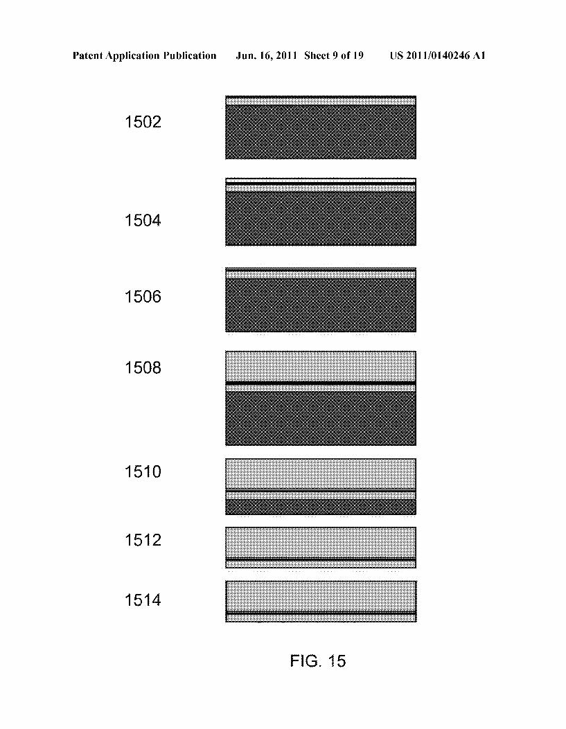
F.G. 12
F.G. 13
Patent Application Publication Jun. 16, 2011 Sheet 8 of 19 US 2011/O140246 A1
% s s
Patent Application Publication Jun. 16, 2011 Sheet 9 of 19 US 2011/O140246 A1
15O2
1504
1506
1508
1510
1512
1514
F.G. 15

Patent Application Publication Jun. 16, 2011 Sheet 10 of 19 US 2011/O140246 A1
1602
1604
1606
1608
1610
1612
F.G. 16
Patent Application Publication Jun. 16, 2011 Sheet 11 of 19 US 2011/O140246 A1
Preparation kickii
3d Eck assaie citie
f :
: 388 Ock ta&ie Kities
f Storage 8xiie
F.G. 17
FG. 18

Patent Application Publication Jun. 16, 2011 Sheet 12 of 19 US 2011/O140246 A1
FIG. 19

US 2011/O140246 A1 Jun. 16, 2011 Sheet 13 of 19 Patent Application Publication

US 2011/O140246 A1 2011 Sheet 14 Of 19 9 Jun. 16 Patent Application Publication
angsa:wogjeº

US 2011/O140246 A1 2011 Sheet 15 Of 19 9 Jun. 16 Patent Application Publication

US 2011/O140246 A1 Jun. 16, 2011 Sheet 16 of 19 Patent Application Publication

Patent Application Publication Jun. 16, 2011 Sheet 17 of 19 US 2011/O140246 A1
V ZV
/ eS s2
S
5.

Patent Application Publication Jun. 16, 2011 Sheet 18 of 19 US 2011/O140246 A1
wim
CD . O C O (f)
C c
CD X cy
3D r - lf t Z
A CN
XXYYX. V A LA A LA A A
7 77 XXX XXXX

US 2011/O140246 A1 Jun. 16, 2011 Sheet 19 of 19 Patent Application Publication
§§

US 2011/0140246 A1
DELTA-DOPING AT WAFER LEVEL FOR HIGH THROUGHPUT, HIGHYIELD FABRICATION OF SILICON MAGING
ARRAYS
CROSS-REFERENCE TO RELATED APPLICATIONS
0001. This application claims priority to and the benefit of co-pending U.S. provisional patent application Ser. No. 61/285,288, filed Dec. 10, 2009, and of co-pending U.S. provisional patent application Ser. No. 61/303,551, filed Feb. 11, 2010, each of which applications is incorporated herein by reference in its entirety. This application is also related to U.S. Pat. Nos. 4,798.598, 4,822,748, 4,882,609, 5,316,586, 5,376,810, 5,701,016, 6,403,963, 7,786,421 and 7,800,040, each of which patents is incorporated herein by reference in its entirety, and all of which are commonly assigned to the assignee of the present application.
STATEMENT REGARDING FEDERALLY FUNDED RESEARCHOR DEVELOPMENT
0002. The invention described herein was made in the performance of work under a NASA contract, and is subject to the provisions of Public Law 96-517 (35 USC 202) in which the Contractor has elected to retain title.
FIELD OF THE INVENTION
0003. The invention relates to systems and methods for processing semiconductors in general and particularly to sys tems and methods that employ dry processing.
BACKGROUND OF THE INVENTION
0004 Solid state imaging detectors, such as charge coupled devices and CMOS imaging detectors, are conven tionally illuminated through the front Surface. In this configu ration, structures designed for circuit operation (including patterned oxides, polysilicon electrodes, and metal intercon nects) cause reduction of quantum efficiency and loss of resolution by absorption and scattering of incident light. Soon after the invention of charge-coupled devices, a back-illumi nated CCD was demonstrated, in which light the imaging detector is flipped upside down and illuminated from the opposite side of the silicon wafer. Back-illumination typi cally requires removal of the low-resistivity substrate and passivation of the exposed silicon Surface. In the case of high resistivity Substrates, Substrate removal is not required, but Substrate thinning and Surface passivation are still required to achieve high, stable quantum efficiency across a broad spec tral range. Various technologies for thinning are described in the literature. 0005 Surface passivation has been a critical part of silicon device development from the beginning. The first successful demonstration of amplification with a solid-state transistor closely followed John Bardeen's seminal paper on the role of Surface charge and rectification at the semiconductor Surface, and the development of integrated circuits in the 1960's was enabled by the discovery of technologies for surface passiva tion with thermal oxides. Virtually all semiconductor devices—including especially solid-state imaging devices— depend for their performance and stability on Surface passi Vation processes. Since the first demonstration of silicon CCDs in 1969, many of the key advances in device perfor mance have been related to the passivation of the Si SiO,
Jun. 16, 2011
Surface, including especially the front-side developments of buried channel devices, and Surface inversion during charge integration (also known as multi-pinned phase, or MPP). Back-illuminated detectors were demonstrated as early as 1974, but the performance of these early back-illuminated devices suffered from the lack of an adequate Surface passi Vation technology. The significance of this problem was real ized by NASA in the aftermath of the 1984 discovery of quantum efficiency hysteresis in CCDs built into the Hubble Space Telescope's Wide Field/Planetary Camera (WF/PC). Instabilities related to Surface traps and poor passivation plagued WF/PC practically up to the 1992 launch of WF/PC II, in which back-illumination was abandoned in favor of phosphor-coated, front-illuminated CCDs. 0006 JPL developed delta-doping in 1992 as a method and device for achieving stable, high ultraviolet quantum efficiency in silicon CCDs (U.S. Pat. No. 5,376,810, Dec. 27, 1994). Initial MBE growths at JPL in 1991 used MBE to grow 5 nm of uniformly boron-doped silicon, as described in Michael E. Hoenk, Paula J. Grunthaner, Frank J. Grunthaner, R. W. Terhune, and Masoud Fattahi, “Epitaxial growth of p-- silicon on a backside-thinned CCD for enhanced UV response.” Proc. SPIE 1656, 488 (1992). In all subsequent growths on CCDS and other imaging detectors, JPL used MBE to grow delta-doped silicon layers for surface passiva tion, as described in Michael E. Hoenk, Paula J. Grunthaner, Frank J. Grunthaner, R. W. Terhune, Masoud Fattahi, and Hsin-Fu Tseng, “Growth of a delta-doped silicon layer by molecular beam epitaxy on a charge-coupled device for reflection-limited ultraviolet quantum efficiency. Appl. Phys. Lett. 61, 1084 (1992). This approach used highly doped silicon to create a strong near-surface electric field and elimi nate the back Surface potential well, thus passivating the silicon Surface and achieving the desired high quantum effi ciency and stability. The development of low-temperature MBE processes at JPL in the 1980's was an important tech nology for the implementation of MBE-growth as a surface passivation technology for CCDs. 0007. There is a need for systems and methods that can provide silicon devices having improved passivation of Sur faces and interfaces (especially over large area devices and/or wafers), in order to provide improvement of operating param eters (such as improved stability, reduced leakage and/or dark current, and improved efficiency), and/or improved manufac turing parameters (such as yield and throughput).
SUMMARY OF THE INVENTION
0008 According to one aspect the invention features a method and apparatus for implementing Surface passivation by quantum exclusion, in which Subnanometer-scale control over Surface structures and materials produces a buried elec tronic surface that isolates the physical surface from the bulk semiconductor material, and prevents the interaction of minority carriers with surface defects. 0009. According to one aspect, surface passivation by quantum exclusion stabilizes the electronic properties of sili con Surfaces and interfaces without requiring low defect den sities at the interface. 0010. According to one aspect, surface passivation by quantum exclusion stabilizes the electronic properties of sili con Surfaces and interfaces without exposing the Surface to process temperatures greater than 600° C. 0011. According to one aspect, the invention features a silicon device. The device comprises a silicon wafer having

US 2011/0140246 A1
the device fabricated on a first surface thereof, and having a second Surface; the silicon wafer having an abrupt doping profile situated adjacent at least one of the first surface and the second Surface, the abrupt profile having a dopant concentra tion at least 10' cm and a dopant gradient at least one decade per nmi; the silicon wafer having at least one of the first Surface and the second Surface electronically passivated irre spective of a density of defects present on the respective one of first surface and the second surface. The term "electroni cally passivated' is defined to mean that charge carriers approaching a Surface from the bulk beyond the abrupt dop ing profile have a reduced likelihood of being recombined at defects on the Surface as compared to a Surface of a silicon material lacking the abrupt profile. 0012. In one embodiment, the abrupt profile has a dopant concentration at least 10 cm and a dopant gradient at least one decade per nm. 0013. In another embodiment, the silicon device com prises a Surface cleaned in a two step gaseous cleaning pro CCSS,
0014. In yet another embodiment, the device comprises a device selected from the group of devices consisting of a CCD device, a CMOS device, an NMOS device, a photodiode, and a silicon Solar cell. 0015. According to another aspect, the invention relates to a molecular beam epitaxy apparatus for processing a silicon material. The molecular beam epitaxy apparatus comprises an epitaxy chamber configured to perform molecular beam epitaxy on a silicon material; a preparation chamber config ured to clean a surface of the silicon material of surface contaminants by an oxidizing plasma process, and configured to remove an oxide from the surface of the silicon material by formation and removal of a volatile silicate, the preparation chamber having at least one mutual communication port with the epitaxy chamber whereby the silicon material can be transferred between the epitaxy chamber and the preparation chamber; a plasma source attached to the preparation cham ber, the plasma source configured to generate an oxidizing plasma; a throttle valve, a controller, and a reactive gas Sup ply, configured to provide reagent gases to the preparation chamber; and pumping equipment configured to provide a reduced pressure within the preparation chamber. 0016. In one embodiment, the plasma source configured to generate an oxidizing plasma is configured to generate an oxygen plasma. 0017. In another embodiment, the preparation chamber configured to remove an oxide from the surface of the silicon material by formation and removal of a volatile silicate is configured to use NH and NF to generate a volatile silicate. 0018. In yet another embodiment, the epitaxy chamber is configured to accommodate at least one silicon material hav ing a dimension of at least 6 inches. 0019. In still another embodiment, the epitaxy chamber is configured to accommodate at least one silicon material hav ing a dimension of at least 8 inches. 0020. In a further embodiment, the apparatus is configured to process the silicon material at a temperature less than or equal to 450° C. 0021. In yet a further embodiment, the silicon material comprises a device selected from the group of devices con sisting of a CCD device, a CMOS device, an NMOS device, a photodiode, and a silicon Solar cell. 0022. In one more embodiment, the silicon material com prises a delta-doped device.
Jun. 16, 2011
0023. In still a further embodiment, the silicon material comprises a device configured to operate under back-illumi nation. 0024. According to one aspect, the invention features a silicon processing method. The silicon processing method comprises the steps of providing an MBE apparatus; provid ing a silicon material to processed; applying an oxidizing plasma to a Surface of the silicon material; reacting an oxide present on the Surface of the silicon material with reagent gases to form a silicon compound volatile at a temperature below 450° C.; and removing the silicon compound to pro vide a clean hydrogen-bonded silicon Surface on the silicon material. The MBE apparatus comprises an epitaxy chamber configured to perform molecular beam epitaxy on a silicon material; at least one preparation chamber configured to clean a Surface of the silicon material of surface contaminants by a process having an impurity removal step, and having an oxide removal step, the at least one preparation chamber having at least one mutual communication port with the epitaxy cham ber whereby the silicon material can be transferred between the epitaxy chamber and the at least one preparation chamber; the at least one preparation chamber having in communica tion therewith a plasma Source configured to generate an oxidizing plasma, at least one throttle valve, at least one controller, and at least one reactive gas Supply configured to provide reagent gases to the at least one preparation chamber; and pumping equipment configured to provide a reduced pressure within the at least one preparation chamber. 0025. In one embodiment, the silicon processing method further comprises the step of performing molecular beam epitaxy on the silicon material. 0026. In another embodiment, the step of performing molecular beam epitaxy on the silicon material comprises performing delta doping. 0027. In yet another embodiment, the silicon material is maintained at a temperature less than or equal to 450° C. 0028. In still another embodiment, the silicon material comprises a device selected from the group of devices con sisting of a CCD device, a CMOS device, an NMOS device, a photodiode, and a silicon Solar cell. 0029. In a further embodiment, the silicon material com prises a device configured to operate under back-illumina tion. 0030. In yet a further embodiment, the at least one prepa ration chamber comprises two preparation chambers. 0031. In an additional embodiment, the impurity removal step is performed in a first of the two preparation chambers and an oxide removal step is performed in a second of the two preparation chambers. 0032. In one more embodiment, the impurity removal step and oxide removal step are repeated multiple times. 0033. In still a further embodiment, one of the first and second preparation chambers is a glove box. 0034. In yet another embodiment, the impurity removal step and the oxide removal step are repeated multiple times. 0035. In one embodiment, the impurity removal step is an oxidation step. 0036. In another embodiment, the oxidation step is per formed using a gas comprising oxygen. 0037. In yet another embodiment, the impurity comprises carbon.
0038. In still another embodiment, the impurity removal step is a reduction step.

US 2011/0140246 A1
0039. In a further embodiment, the reduction step is per formed using a gas selected from the group consisting of H, NH, and mixtures thereof. 0040. In yet a further embodiment, the impurity comprises carbon. 0041. In an additional embodiment, the oxide removal step is performed using a gas selected from the group con sisting of NF, NH, N, H. and mixtures thereof. 0042. In one more embodiment, the oxide removal step is performed using a fluorine containing gas. 0043. In still a further embodiment, the fluorine contain ing gas is selected from the group consisting of HF, NF, and F and mixtures thereof. 0044. The foregoing and other objects, aspects, features, and advantages of the invention will become more apparent from the following description and from the claims.
BRIEF DESCRIPTION OF THE DRAWINGS
0045. The objects and features of the invention can be better understood with reference to the drawings described below, and the claims. The drawings are not necessarily to scale, emphasis instead generally being placed upon illustrat ing the principles of the invention. In the drawings, like numerals are used to indicate like parts throughout the various W1WS.
0046 FIG. 1 is a schematic drawing of the electronic band structure in a back illuminated silicon imaging detector. The detector is depicted in cross section, with the back surface on the left and the front surface on the right. The front surface electrodes, consisting of multiple layers of oxide, polysilicon, and metal, are shown schematically on the right, and an oxide formed on the back surface is shown schematically on the left. Light enters the detector from the back Surface, generating free electrons in the conduction band. In order to be detected, the electrons must move by drift and diffusion into the buried channel near the front Surface. However, positive charge at the back Surface creates a backside potential well, which can trap Some of the photogenerated electrons. 0047 FIG. 2 is a diagram showing the near surface con duction band edge calculated for four different methods of Surface doping. The potential energy is plotted in eV, and depth from the Surface is given in nanometers; for compari son, the minimum 1/e absorption depth in silicon is approxi mately 4 nm, and thermal energy is approximately 0.015 eV at -100 C. In order to prevent trapping of UV-generated photoelectrons in the backside potential well and eliminate quantum efficiency hysteresis, a sharply peaked dopant pro file is essential to creating a strong electric field within a few nm of the Surface. Only delta-doping can achieve this goal. 0048 FIG. 3 is a diagram showing the calculated elec tronic wavefunctions showing one of the essential features of Surface passivation by quantum exclusion. The figure shows the calculated conduction band edge and ground state wave function of electrons “trapped between the surface and the delta-doped layer. The sharply peaked Surface potential cre ated by delta-doping reduces the backside potential well of FIG. 1 to a quantum well, nearly 1 eV in depth and <2 nm in width. Quantum confinement of electrons in this well increases the ground state energy of “trapped’ electrons sig nificantly above the conduction band edge, and the wave function extends into the bulk semiconductor where there is a high density of lower energy states. This indicates that there is no bound state for electrons at the Surface, and electrons
Jun. 16, 2011
produced in the near Surface region can rapidly tunnel through the delta-layer to lower energy states in the bulk silicon. 0049 FIG. 4 is a diagram showing the quantum efficiency measurements of a delta-doped, p-channel CCD, demonstrat ing near reflection-limited quantum efficiency from the UV through the near infrared. Half of the CCD back surface has been coated with a bilayer antireflection coating. For com parison, the silicon transmittance is plotted in the figure for coated and uncoated regions. 0050 FIG. 5 is a diagram showing the quantum efficiency measurements of a delta-doped n-channel CCD, showing reflection-limited quantum efficiency from the soft X-ray through the visible regions of the spectrum. Note that the data shown in the figure have been corrected for quantum yield. For comparison, the silicon reflection limit is shown in the figure, along with quantum efficiency measurements of an antireflection-coated, delta-doped CCD. 0051 FIG. 6 is a diagram showing the quantum efficiency of a delta-doped CMOS imaging array, shown without an antireflection coating. As with delta-doped CCDs, the quan tum efficiency of delta-doped CMOS arrays is limited prima rily by reflection from the silicon surface. Most of the improvement in quantum efficiency achieved with back illu mination results from the elimination of absorption in the front Surface structures as a loss mechanism. Delta-doping passivates the silicon surface in the thinned CMOS imaging array, which is essential for the elimination of excess dark current during normal operation of the device. For compari son, both back-illuminated and front-illuminated quantum efficiencies of the delta-doped CMOS device are plotted in the figure. 0.052 FIG. 7 is a diagram showing the quantum efficiency data from a delta-doped CCD taken over a three-year timespan, demonstrating the long-term stability of Surface passivation by delta-doping. 0053 FIG. 8 is a diagram showing the quantum efficiency data comparing CCDs produced by several different device manufacturers, showing that delta-doping produces repeat able performance independent of variations in CCD design and process parameters. 0054 FIG. 9 is a diagram showing the quantum efficiency data from several p-channel CCDs, showing the dependence of the performance on cap layer thickness grown by molecu lar beam epitaxy. The highest quantum efficiency is observed for the two thinnest cap layer thicknesses. As expected from quantum mechanical calculations similar to that illustrated in FIG. 3, trapping of photogenerated charge at the Surface can be prevented by placing the delta-layer within a few nm of the Surface. 0055 FIG. 10 is an image of a 150 mm silicon wafer with CMOS imaging that has been bonded to a support wafer and thinned to 5 microns. 0056 FIG. 11 is an image of a 2 kx4 k delta-doped, p-channel CCD in a prototype package. 0057 FIG. 12 is an image of a USAF test pattern taken using a 2 kx4 k delta-doped, p-channel CCD. Sharp features are indicative of full depletion of this 250 micron thick, device fabricated on an ultrahigh purity silicon Substrate. 0058 FIG. 13 is an image of a 3.5 kx3.5 k delta-doped, p-channel CCD in a prototype package. 0059 FIG. 14 is a diagram that shows a schematic cross section of an AR-coated, delta-doped CCD that was bonded to a silicon handle wafer prior to thinning and delta-doping. In

US 2011/0140246 A1
this figure, through-hole Vias have been patterned on the handle wafer and filled with metal in order to contact the buried CCD bond pads. This bonding process provides mechanical Support for the thinned device, which is a key step in wafer-scale MBE processing. 0060 FIG. 15 is a diagram illustrating in cross sectional view the process flow showing device structure at various stages of the processing, including bonding, thinning, Surface preparation, MBE growth, post-growth surface passivation (optional), and AR coating (optional). 0061 FIG. 16 is a diagram illustrating in cross sectional view the process flow showing final steps, including AR coating, patterning, etching, and packaging. 0062 FIG. 17 is an image of a Veeco Gen200MBE system showing cluster tool and various modules for automated wafer transfer, storage, and processing. 0063 FIG. 18 is an image of 150 mm wafer that has been patterned processed to form multiple imaging devices and test Structures.
0064 FIG. 19 is a flat-field ultraviolet image taken with delta-doped CCD, showing excellent uniformity. 0065 FIG. 20 is a diagram showing a schematic represen tation of bonding and thinning process. 0066 FIG. 21 is a diagram showing the steps in cleaning a wafer Surface using conventional processing. 0067 FIG.22 is a diagram showing a schematic represen tation of in vacuo wafer-level Surface preparation processes. 0068 FIG. 23 is a diagram showing a schematic represen tation of an in vacuo native oxide removal process, producing a clean, hydrogen-terminated surface that is ready for MBE growth. 0069 FIG. 24 is a schematic diagram showing an in vacuo surface preparation chamber in the JPL MBE system. 0070 FIG. 25 is a schematic diagram of gas manifold providing process gases to the in vacuo Surface preparation chamber in the JPL MBE system. 0071 FIG. 26 is an image showing in the foreground an 8 inch silicon wafer on a platen being transferred between a glove box and a load lock, with components of the Veeco GEN200 Silicon MBE apparatus to which the glove box and load lock are connected visible in the background.
DETAILED DESCRIPTION
Delta Doping
Passivation of Semiconductor Surfaces by Quantum Exclusion
0072 Growth of highly doped silicon by molecular beam epitaxy, first demonstrated at the Jet Propulsion Laboratory (JPL) in 1991, is the only surface passivation technology that eliminates quantum efficiency hysteresis in back-illuminated Scientific imaging arrays. Delta-doping Tests specifically designed to characterize the stability of delta-doped detectors and to search for signs of hysteresis showed no trace of hysteretic response. Quantum exclusion both explains the exceptional performance of delta-doped CCDs, and extends the concepts and applications to existing devices, novel devices, and new applications that are relevant to NASA's conduct of aeronautical and space activities. 0.073 Surfaces and interfaces in semiconductors are the Source of a variety of problems in semiconductor devices. Surface/interface states can act as electronic traps and centers of recombination and generation that can have multiple del eterious effects on device performance, including dark cur
Jun. 16, 2011
rent, noise, and instabilities in semiconductor devices, and thus present a long-standing problem in semiconductor device technology. Passivation of Surfaces and interfaces mitigates these problems. One aspect of this more general problem is surface passivation in Solar cells, photodiodes and back-illuminated imaging detectors. This is illustrated by FIG 1.
0074. In state-of-the-art devices, surface passivation is addressed by two strategies that can be used alone or in combination. For example, in silicon Solar cells, the lowest reported Surface recombination Velocities (a measure of the effectiveness of Surface passivation) are achieved using a combination of these strategies. In the first approach, defects at Surfaces and interfaces are eliminated, neutralized, or oth erwise electrically deactivated through chemical passivation and/or growth/deposition of a low-defect Surface. Examples of this strategy include the formation of high quality SiO, layers on a silicon Surface in order to minimize the Surface defect density, and the chemical passivation of defects with atomic hydrogenby, for example, annealing informing gas or ion implantation and thermal activation. Second, chemisorp tion and/or surface doping methods can be used to create an electric field near the semiconductor surface, in order to bias the Surface into accumulation and prevent minority carriers from interacting with surface defects. A great deal of effort has gone into developing passivation layers and near-Surface dopant profiles for optimal performance of solar cells, UV photodetectors, and back-illuminated imaging detectors. Examples of Surface passivation technologies developed for back-illuminated imaging detectors include the UV flood, platinum flash gate, chemisorption, shallow implantation of dopants, shallow diffusion of dopants, and delta-doping. (0075. Two of the major difficulties with the various tech nologies for Surface passivation methods lie with the various instabilities associated with surface states and defects that affect device performance, and the susceptibility of the sur face to degradation by radiation or exposure to UV radiation. Quantum efficiency hysteresis has plagued scientific Solid state imaging detectors ever since NASA first invested in charge coupled devices (CCDs) in the early 1970's. Instabili ties are especially problematic in the technologically impor tant area of deep ultraviolet photodetectors and imagers, because deep ultraviolet photons and other forms of ionizing radiation carry Sufficient energy to damage the Surface, alter ing Surface charge and producing electrically active defects. Exposure to ionizing radiation is a serious problem for both field-induced passivation and doping passivation. 0076. Here we focus on doping the surface. In general, doping the Surface of an imaging detector mitigates, but does not completely eliminate, trapping of photogenerated charge at the surface. Surface charge depletes the surface to a depth that depends on the amount of charge in the oxide and the spatial distribution of ionized dopant atoms beneath the sur face. Variation of the Surface charge causes variation in the width of the depletion layer, which in turn causes variation in the quantum efficiency. In particular, the width of the surface depletion layer may vary under illumination. Changes to the depletion layer width may be permanent (e.g., UV-induced creation of defects at SiO, Si interface), or temporary (e.g., UV-adsorbed ions, and/or dynamic trapping of mobile charge carriers at the Surface). This phenomenon, known as quantum efficiency hysteresis, is a major problem in Scientific imaging detectors.

US 2011/0140246 A1
0077 One solution involves delta-doping the surface of back-illuminated CCDs and CMOS imaging arrays to passi vate the Surface, and, uniquely among known Surface passi Vation methods, completely eliminate quantum efficiency hysteresis. Delta-doping is an example of Surface passivation by quantum exclusion. 0078 We now present a quantum mechanical formulation of the problem and its solution, which provides a new expla nation for the observation that delta-doped CCDs have proven impervious to the damaging effects of deep ultraviolet light and other forms of ionizing radiation. It is stipulated that the concept of surface passivation by quantum exclusion is more general both in method and application; that other methods of creating the required near-Surface electronic potential can be developed based on these concepts; and that passivation by quantum exclusion may find useful application in a larger class of semiconductor devices and applications than the above-cited examples of Solar cells, photodetectors, and back-illuminated Solid-state imaging devices. 0079 Quantum mechanical exclusion of minority carriers from the Surface results in exceptional performance and sta bility of imaging detectors. Because of the relationship between wave functions and electronic potential of doped semiconductors, a strongly-peaked, near-surface doping pro file creates an electronic potential that effectively excludes minority carriers from interacting with the Surface. Concep tually, this results in the formation of an electronic surface that is buried beneath the physical Surface, thus isolating and decoupling surface states and defects from interfering with device operation. This decoupling of the electronic and physi cal Surfaces is extremely important in delta-doped imaging detectors, because it prevents Surface coatings, chemisorbed molecules, and external fields from affecting the stability of a delta-doped detector. 0080. The isolation of electronic and physical surfaces by quantum exclusion is important, but this represents only part of the potential for this technology. The concepts and meth ods presented here can be generalized to encompass many more device structures and technologies. The epitaxial growth technology used for delta-doping Surfaces, together with the theory of surface passivation by quantum exclusion, are readily extendable to more complicated structures and functions, especially with respect to two and three dimen sional patterned structures. The ability to fabricate semicon ductor dopant profiles with atomic-scale precision enables the manipulation of quantum mechanical states and quantum transport of electrons and holes. These technologies can thus be applied in the design, modification, and development of many conceivable device structures, seeking either optimal performance of existing devices or developing new devices and structures.
0081. We define quantum exclusion as the effective isola tion of minority carriers from the near-surface region of a semiconductor based on the probabilistic laws of quantum mechanics as applied to dopant profiles that can be precisely controlled on an atomic scale. According to quantum mechanical formalism, semiconductor structures formed on length scales comparable to the effective Bohr radius of elec trons and/or holes are characterized by quantized energy states, which effectively increases the electronic band gap within such structures. It was predicted in the 1950's, and experimentally verified in the 1960's that electronic states can be quantized near semiconductor Surfaces, such as for elec tronic states in the inversion layer of a silicon Surface that was
Jun. 16, 2011
subjected to a strong electric field. Majority carriers in the inversion layerform a two-dimensional electrongas, in which the energies, density of states, and mobility are strongly influ enced by quantum confinement. I0082 In particular, quantum mechanical calculations of electronic states in the vicinity of a delta-doped surface explain the observed 100% internal quantum efficiency and stable response in back-illuminated, delta-doped charge coupled devices (CCDs). Delta-doping presents a unique case among Surface doping technologies, in that all of the dopant atoms are concentrated at a fixed distance from the Surface. Using the atomic-scale control over crystal composition made possible by molecular beam epitaxy (and to a lesser extent by some other crystal growth technologies), a sharply peaked dopant profile can be formed with precision, Such that the peak is formed within a few nanometers of the silicon surface (see FIG. 2). Such a sharply-peaked dopant profile is termed delta-doping, in reference to the mathematical delta function. Delta-doped CCDs have been shown to exhibit nearly 100% internal quantum efficiency throughout the vis ible and ultraviolet regions of the spectrum. Furthermore, delta-doped CCDs do not exhibit quantum efficiency hyster esis even under exposure to Lyman-alpha radiation at 121.6
I0083. Delta-doped CCDs therefore offer a concrete example that Surface passivation by quantum exclusion is not only possible, but practical and useful in the design of semi conductor devices. The spreading-out in space of both minor ity and majority carriers in semiconductors is described math ematically in probabilistic terms by wave functions. One method for calculating the wave functions, used in the litera ture to describe surface inversion layers in semiconductors, is to self-consistently solve the Poisson and Schrödinger equa tions for a specific semiconductor device structure. The quan tum mechanical formalism used to describe semiconductor inversion layers, when applied to the back Surface of a delta doped CCD, shows that electronic states in the backside potential well are strongly coupled to the lower-energy con duction band states in the bulk semiconductor (see FIG.3). In the case of delta-doping, the dopant profile, and hence the electronic potential, is so strongly peaked near the Surface that the wave functions of minority carriers in the near-Sur face potential well cannot be fully confined to the surface region, but instead spread well into the region where the conduction band forms a continuum in energy. Under these conditions, the 'Surface states are only quasi-bound, and minority carriers in these states are rapidly transported away from the Surface by quantum mechanical tunneling. In effect, there are no bound states for minority carriers at the back Surface, resulting in a highly effective passivation of the Sur face. Thus, in this technologically important example, the “backside potential well of thinned, delta-doped, back-illu minated imaging detectors is effectively eliminated in the probabilistic sense of quantum mechanics, and trapping of electrons at the Surface becomes impossible. I0084 Surface passivation by quantum exclusion results in the effective isolation of the physical surface, where are located Surface defects and traps, from the electronic Surface, which is defined in space by the position of the buried delta doped layer. In the case of delta-doping, the theory provides a quantitative means of determining how sharply peaked the dopant profile must be, how close the peak must be to the Surface, and what concentration of dopant atoms must be achieved in order to achieve quantum exclusion. More impor
US 2011/0140246 A1
tantly, the theory and concepts of quantum exclusion devel oped to analyze this one dimensional problem can be gener alized to solve problems in two and three dimensions. For example, by combining semiconductor patterning technolo gies with molecular beam epitaxial growth technologies, it will be possible to engineer three dimensional "electronic Surfaces and interfaces to develop new applications and novel nanostructured devices. A number of problems having to do with surface states and defects at the front surface of semiconductor devices may be amenable to this approach. For example, Surface-generated dark current currently con stitutes one of the major limitations to the performance of CMOS imaging detectors. Problems such as this, in which semiconductor Surfaces and interfaces introduce problems Such as excessive Surface-generated dark current, trapping of charge at interfaces, and so-called "spurious charge' injec tion, can be approached by developing two- and three-dimen sional structures that use quantum exclusion to isolate Surface states and defects (the physical surface) from the electronic surface and active volume of the device. Other applications of quantum exclusion may be found. 0085. One example of practical utility involves telescopes. At the heart of every ground-based astronomical telescope and every telescope launched by NASA into space are solid state imaging detectors, which transform light into digital images with exceptional sensitivity, resolution, and dynamic range. It is no Small task to achieve Such precision. Light incident on the Solid-state imaging array is converted into charge, which is collected over the entire array and measured with sensitivity that can approach the level of single electrons, and yet maintain exceptional photometric precision over a dynamic range covering four to five orders of magnitude. At this level of precision, defects in the detector material become extremely important. From a materials science perspective, many of the challenges currently faced by developers of sci entific imaging detectors come down to controlling the Sur faces and interfaces comprising the Solid-state device. More generally, controlling electronic states at semiconductor Sur faces and interfaces is the key to virtually all electronic devices.
Fabrication Processes
I0086 We now describe fabrication processes for devices using back illumination technology based on delta-doping, thinning, and packaging. The back illumination technology can be applied to CCD wafers available from a commercial silicon “foundry' or vendor of processed wafers. Delta dop ing technology when applied to a variety of CCDs and CMOS imaging arrays has enabled 100% internal quantum efficiency (QE), high stability in the QE, uniformity of response, and low dark current. It has been demonstrated that the applica tion of this technology to CCD designs advances the state of the art as measured by Such essential performance parameters as quantum efficiency (QE), spectral range, dark current, stability, uniformity, dark current, point spread function, and sensor flatness. 0087 Important features of the technology include Delta doped back surface passivation for 100% internal QE with exceptional stability and photometric accuracy; robust Sup port and thinning technology for 100 micron thickness while maintaining flatness; and integrated AR coatings for opti mized performance in different spectral bands. 0088. One application is in the Large Synoptic Survey Telescope (LSST) which expected to break ground in more
Jun. 16, 2011
than wide field imaging. In particular, great attention is expected to achieve accurate knowledge of photometric pre cision, astrometric precision and PSF (point-spread func tion). Each one of these attributes is expected to directly result in major advances in astronomy (e.g. Galactic archeology, Galactic dynamics and stellar kinematics and weak lensing). I0089. The sensor, comprising Charge Coupled Devices (CCDs), is critical to the success of LSST. Sensitivity demands the highest possible quantum efficiency over the visible bands as well as accurate knowledge of linearity and flat surfaces without intrinsic variations. Delta-doped CCDs satisfy these demanding requirements. Indeed, there is evi dence that delta-doped CCDs are superior to conventional CCDS.
0090 There is great interest in these devices for both upgrading present instruments at the Mount Palomar obser vatory (the venerable Double Beam Spectrograph) and the Keck Observatory (Echellete Imaging Spectrometer and a recently proposed new seeing limited Echelle Spectrograph). 0091 An end-to-end post fabrication device processing to produce high performance silicon imaging arrays of various designs for the UV to NIR range of the spectrum is described. Nonequilibrium crystal growth techniques are used to engi neer the device bandstructure to deliver maximum QE, mini mized leakage and dark current, and optimum spectral range in a stable and reliable device structure.
0092 Elements of the technology include development of n-channel p-type delta doped CCDs, extension of the CCD response for EUV and low energy particle detection, devel opment of high-speed delta doped CCD cameras and devel opment of delta doped p-channel LBNL CCDs. Additional features include the growth of delta-doped layers on fully processed n-channel CCDs in order to modify the interface bandstructure and achieve 100% internal QE, and growth processes for n-type delta doping for high purity p-channel CCDs with near-100% internal QE. Detector processing ele ments include thinning of n-channel conventional CCDS and CMOS arrays down to 5 micron and chemical mechanical polishing. 0093. The end-to-end processes for producing back-illu minated silicon imaging arrays start from fully-fabricated devices, and use delta-doping technology to extend the spec tral range of the imagers to cover the entire UV-NIR spectral range with 100% internal QE (nearly 100% DOE in UV-NIR with AR coating), and enable excellent stability, uniformity, and low dark current. This technology has been Successfully demonstrated on a variety of CCDs and CMOS designs and formats. The exceptional performance of delta-doped devices has been Verified by many groups, and demonstrate that delta doped detectors provide the exceptional stability required for precision photometry. 0094. In addition to the high performance that they enable, the processes are done at low temperature, and are therefore entirely compatible with VLSI device structures. This pro vides the flexibility to work with virtually any device design. 0.095 Delta doping is a technique that uses molecular beam epitaxy (MBE) to passivate a back illuminated silicon imaging array by placing a very high concentration of charge near the back surface of the imager. Delta-doped detectors have been demonstrated with 100% internal QE from the extreme UV (n-channel) through the near infrared (p-chan nel) with dark current of 0.5 electrons/pixel/hour (at -130°

US 2011/0140246 A1
C.), and exceptional uniformity and photometric stability. Delta doping is a low temperature process that is fully com patible with VLSI fabrication. 0096. Delta doping is an atomically precise epitaxial crys
tal growth technology. This process creates a highly doped silicon layer that is confined to several monolayers (~2 nm) at the back surface of a back-illuminated CCD. This effectively passivates the Surface in Such a way that it is extremely stable to environmental variation as shown in FIG. 3. 0097. Because the delta doped layer is so thin, there is essentially no optical loss in this layer, even at very short wavelengths (UV) as shown in FIG. 5. 0098. Delta doping is compatible with a broad range of antireflection coating designs and materials. The response is easily tailored by integration of AR coatings of choices. Delta doping does not require any post process annealing and it produces very uniform flat fields. 0099. One of the most important features of delta doped imaging arrays is the stability of their response as a function of time (See FIG. 7), environment, temperature, and illumi nation. The delta doping process is reproducible and has been demonstrated on many CCD formats manufactured by vari ous vendors (FIG. 8). 0100 FIG. 9 demonstrates both the precision control afforded by MBE and the importance of having that control for back illuminated imager performance. A thin electrode is essential to QE and more importantly the stability of QE. For example, ion implanted layers are thicker than delta layers and ultimately are limited by the physics of the process. FIG. 9 shows the effect of embedding the delta layer (charge) at different depths below the back surface of the device, an exercise in atomic layer control of composition and position of the critical charge that is only possible by MBE. When the delta layer is closest to the back surface (1.5 nm cap) there is essentially no optical loss in the back Surface contact over the entire range tested (250-1100 nm). The exceptional stability offered by delta doping comes from high quality epitaxial material and precise control over the dopant profile.
Bonding. Thinning and Surface Preparation Prior to MBE Growth
0101 Fully processed wafers of CCD imagers have to be prepared for the Surface passivation by Suitably attaching a support wafer and then thinning the wafer to remove its low resistivity bulk silicon. Low-temperature oxide bonding is used to attach the Support wafer. This bonding process can be achieved without damaging the processed circuitry as would occur under high temperature oxide bonding. The bonding process has been developed by others, is well known, and described elsewhere. Briefly, in a sequence of oxide applica tion and flattening, the layered structure of the processed wafer is given a thick oxide coating that is Smooth and flat. The wafer bond is achieved by mating the now-smooth pro cessed wafer to an equally smooth Substrate wafer. In low temperature oxide bonding, the contact Surfaces of the two wafers are meticulously cleaned of all particles. The particle cleaning process must remove all particles larger than 50 nm. The wafers are aligned and allowed to make contact. The initial point of contact draws the two Surfaces tightly together and the region of bonded contact rapidly spreads over the entire surface. A suitable attachment of wafers is able to Sustain its bond through the remaining processing steps. Spe cifically, the bond must resist shearing action in wafer grind ing and Chemical Mechanical Polishing (CMP). Addition
Jun. 16, 2011
ally, during MBE growth temperatures up to 450 degrees C. the oxide used in the bond must not release gasses that blister in the interface. The choice of oxide growth process and Subsequent anneal steps play a large role in preventing blis ters.
0102 The backside of the CCD wafer is ground and pol ished with CMP down to a distance of 10 microns from its epitaxial layer. The substrate wafer protects the CCD wafer from mechanical harm. The next step is to etch to the epitaxial layer using a process that has been developed by others, is well known, and described elsewhere. Briefly, Hydrofluoric, Nitric, and Acetic acids (HNA) are mixed in a ratio of 1:3:8 and, under ultrasonic agitation, allowed to etch the bonded wafer pair. The bonded wafer is removed after the HNA has reached the CCD wafer's epitaxial layer. The 1:3:8 composed HNA automatically stops etching at the five-order-of-magni tude change in resistivity at the epitaxial layer. Additional brief etches in 1:40:15 HNA and Hydrofluoric acid with KMnO, often help to remove stains and discolorations. 0103) One important feature is the dedicated chemical mechanical polishing (CMP) and chemical etching facilities and procedures. These procedures have been applied at the die or wafer level to high-speed CMOS imagers, high purity and thick LBNL CCDs with extended red response, and to hybrid silicon imaging arrays. FIG. 10 shows a 6-inch wafer thinned down to six microns while it is attached to a Support Substrate. Polishing is achieved with high precision using in-house CMP. 0104 For fully depleted CCDs, the delta doped layer serves the additional important role of a uniform and stable back-surface contact for substrate biasing to achieve full depletion for excellent point spread function. An important feature of the process is that it is low temperature and can be applied to fully fabricated CCDs, complete with metalliza tion. This enables delta doping technology to be combined with any manufacturers CCD design with minimal effort, providing a universal Solution for back Surface passivation and electrical contact.
High Throughput Processes and Manufacturability 0105. An important element of a high yield high through put process is to increase the capacity and yield of delta doping processes so that complete wafers containing fully fabricated devices can be delta doped. An 8-inch MBE with multiple wafer capacity is use. Multiple wafers can be pre pared and loaded into the machine and delta doping a lot run can be accomplished in a matter of days. 0106 FIG. 14 is a diagram in schematic form that shows a back illuminated CCD having a flat, 100-micron thick CCD with high and stable QE over the 400-1000 nm wavelength range. A handle wafer is used as a fanout to mirror the bond pads of the CCD at their exact locations. The handle wafer is prepared by producing metal-filled via holes in thick silicon wafers. Oxide is deposited on the wafer for direct low tem perature wafer-wafer bonding. In parallel, the CCD wafer is also prepared by deposition and planarization of oxide on the circuitry frontside surface. After low temperature direct bonding, the device is robust and can be thinned down to 100-micron. Devices are then delta doped, AR coated, and individually packaged, screened and fully tested.
Device Fabrication
0107 We now describe several procedures for fabricating back illuminated devices having delta doped regions.
US 2011/0140246 A1
0108 FIG. 15 is a flow diagram that illustrates steps in the fabrication of devices using a technique involving full wafer support. At step 1502, there is provided a front surface CMOS structure defined in 10um epion a 8" substrate, which is ~800 um thick. Step 1502 shows a starting device. The substrate is shown as dark gray, silicon epilayer comprising the device is shown as light gray, and the thin dark layer at top comprises the electronic structures patterned on the silicon epilayer that perform essential device functions. At step 1504, a thick oxide is deposited on the front surface of the wafer. Step 1504 show the deposition of a thick dielectric layer as preparation for bonding. At step 1506, the oxide is planarized. Step 1506 shows the planarization of the Surface as preparation for bonding. At step 1508, the wafer is bonded to a silicon support wafer. At step 1510, the device layer is CMP to approximately 50 um thickness. Step 1510 shows coarse thinning (e.g., grinding, polishing) to reduce the thickness of the device substrate. Step 1512 shows ex vacuo surface preparation steps, including final chemical thinning and Surface prepara tion prior to entry into the vacuum system. At step 1512, an etch in HNA chemical etch is used to expose the epi back Surface. In some cases, HNA mixtures can produce Si etch rates well over 100 um/min, such as Spinetch products from General Chemical, 90 East Halsey Road, Parsippany, N.J. 07.054. At step 1514, the wafer is chemically cleaned to pre pare for MBE growth. Step 1514 shows in vacuo surface preparation and MBE growth as described in this application. 0109 MBE growth adds very little material to the wafer. A diagram that might be provided would show little physical change, because the thicknesses involved are so Small. The MBE growth procedure includes the steps of back surface preparation in a glove box having a nitrogen atmosphere, including a UV oZone and HF spin cleaning, and loading devices into a multiwafer platten on an 8" MBE machine; performing the MBE growth of the delta-doped layer, approximately 3 nm thick; growing an oxide layer, for example by Steam oxidation, such as could be done in a glove box just by letting wafers sit in high humidity for 30 minutes: and applying an AR coating. From this point on, the back Surface must not be exposed to chemicals or contaminants that could affect either the AR coating or delta-doped layer. The delta-doped layer is extremely robust, but it is very thin, and the AR-coating must be kept free of contaminants that might absorb UV light. 0110 FIG. 16 is a flow diagram that illustrates packaging steps in the fabrication of devices according to another embodiment. At step 1602, thick photoresist is deposited, in quantity sufficient to withstand reactive ion etching (RIE). Step 1602 shows the deposition of mask material (e.g., pho toresist) on the back surface of the device structure from Step 1514. At step 1604, the photoresist is patterned, with a pattern determined by the size and position of bond pads. It is pref erable to have large bond pads, to expose a larger area for wire bonding. Step 1604 shows the patterning of mask material to expose the back surface over the bond pads. At step 1606, the RIE is performed to expose the bond pads from underneath the wafer. Approximately 10 um of silicon is removed to expose the pads. Step 1606 shows etching through the silicon epilayer to expose device bond pads from the back. At step 1608, metal is deposited to form a contact layer. Possible methods for the deposition include the use of shadow masks, ALD, or electrodeposition. Step 1608 shows deposition of contact layer (which is optional). At step 1610, the photoresist is stripped and the devices are cleaned. Step 1610 shows the
Jun. 16, 2011
stripping of mask material and cleaning the devices. At step 1612, a package Substrate is applied and the devices are wire bonded to contact pads. Step 1612 shows dicing the wafer and package individual devices.
Vacuum Integrated Selective Chemical Removal of Native Oxide Prior to MBE Growth
0111 Molecular Beam Epitaxy (MBE) is a technique used for the growth of crystalline materials on a chosen Substrate. In conventional practice, to attain the required material prop erties in the MBE-grown film, the substrate surface is care fully prepared prior to MBE using a combination of UV oZone exposures, and aqueous HF spin cleans to selectively remove the native oxides and Surface contamination known to form on silicon substrates after air exposure. However, this process is laborintensive, is known to leave residue, and is not readily Scalable to processing of large Substrates (6" diameter and greater). 0112 Processes that utilize gaseous or vapor phase com pounds are readily Scalable to large Substrate areas. Recent work published in the open literature and US patents show that surface pretreatments combining gas-phase mixtures of NH, NF, and HF have successfully removed the native oxide from silicon. As these processes have shown to be selective, they have typically been employed to clean oxide from silicon transistors prior to forming contacts. 0113. As these reactions occur at relatively low substrate temperatures (100 C and below), these same process condi tions are directly ammenable to use as a Surface pretreatment prior to low temperature (<500° C.) MBE-growth. However, to achieve the same Surface quality on UV-Vis detectors using a “dry” process, it is necessary to replicate the functionality of the two discrete steps (UV-ozone and HF spin clean) of the JPL baseline process. As described herein, these two steps are integrated into one preparation chamber vacuum integrated on a cluster tool with an MBE-growth chamber. It is also feasible to have two separate vacuum integrated preparation chambers that separate these two Surface preparation steps. 0114 Turning to the single preparation chamber embodi ment, a plasma source is used to create reactive ionic and/or atomic species (hydrogen, oxygen, argon) and/or oZone to clean carboneous residue from the substrate surface. It is recognized that the same reactive clean could also be com pleted in a vacuum integrated chamber using any one of several different methods and equipment that generate reac tive ionic and/or atomic species (hydrogen, oxygen, argon) and/or OZone. These might include, but are not limited to: a remote plasma source, a UV lamp, a direct ICP, ECR, RIE, or other plasma Source, or a thermal anneal chamber for intro duction of reducing, oxidizing, and/or inert gases. 0115 The step to remove carbonaceous residue is subse quently followed by a step to remove the silicon oxide from the surface of the silicon. There are many possible embodi ments of this oxide removal process. A preferred method utilizes an exposure to NH and/or fluorine containing gases. The fluorine containing gases include NF, F, and HF. These gases can be introduced concurrently or sequentially. The gases may also be broken down utilizing a remote or direct plasma Source to generate more ionic and/or atomic reactive species. These gases react with the oxide on the silicon Sub strate to form a volatile product that is pumped away. The result is a hydrogen terminated silicon Surface, ready for MBE-growth.
US 2011/0140246 A1
0116. A preferred application of this method is to concur rently add NH and NF in a ratio of greater than 2:1 through a remote plasma source. The silicon Substrate is kept at a temperature below 100° C. during this exposure. The reactive species generated by the plasma source react with the silicon oxide to form an ammonium hexafluorosilicate layer. When the NH and NF are combined in the right ratio, the reaction is extremely selective to silicon dioxide and does not etch the underlying silicon. Once the reaction is complete, the plasma source is shut off and temperature of the silicon substrate is raised above 100° C. At the higher temperatures the ammo nium hexafluorosilicate layer becomes Volatile and it evapo rates or sublimes from the silicon surface. As stated earlier, the result is a hydrogen terminated silicon Surface, free of impurities and ready for MBE-growth. 0117. While the above is a preferred embodiment of the dry process for oxide removal, it is expected that the NH and NF reagents could be replaced by a suitable combination of other nitrogen, hydrogen, and fluorine containing gaseous or vapor species, such as hydrogen, nitrogen, hydrazine, HF Vapor, and F gas. 0118. These two steps, oxidation to remove carbonaceous residue and oxide removal, can be repeated multiple times, if desired, to improve the cleanliness of the silicon surface. The oxidation step will grow a new silicon oxide layer on the hydrogen terminated silicon Surface, which can then be etched away by the NH and NF oxide removal step. Because of the differences in free energy of different crystallographic surfaces or planes in a crystal, repeated oxidation and oxide removal may also provide a more uniform Surface, for example by removing Small asperities of dimensions of one or more atOmS.
0119) An important improvement in cleaning the wafers prior to MBE growth has been developed. This process for chemical removal of native oxide prior to the MBE growth can be practiced within the MBE apparatus. Such a process is expected to provide better cleanliness, less difficulty in wafer handling, and improved throughput and yield. 0120 FIG. 20 is a diagram that illustrates some prepro cessing steps prior to native oxide removal, in which an imag ing device is attached to a Support wafer, and the imaging device is then thinned, leaving a native silicon oxide layer that is contaminated with carbon residue. 0121 FIG. 21 is a diagram that illustrates cleaning tech nology using conventional processing techniques. Carbon is cleaned using a UV Ozone process, and HF Spin Clean is used for final Surface preparation steps to remove the native oxide. Until now, these processes have been performed in dedicated systems that cannot be easily integrated with Si MBE technology. 0122 FIG. 22 is a diagram that shows the process flow in a new wafer cleaning technology that is compatible with Si MBE processing, and can be implemented in an MBE system. The process is a dry process performed in a vacuum chamber. The carbon residue is removed with an oxygen plasma clean. The native oxide is then removed using a NH+NF gaseous chemical cleaning process. In the new process, the apparatus needed for plasma and thermal cleans is mounted to a cluster tool, enabling fully integrated, fully automated processing with the subsequent Si MBE. As stated earlier, these dry process cleaning steps can be separated into dedicated cham bers (one each for carbon removal and oxide removal) if desired. The reactive species for dry cleaning of these silicon substrates may also be generated by UV or other alternative
Jun. 16, 2011
methods that do not involve a plasma. It is expected that a plasma of other chemical species than oxygen can also be used to remove carbon from the surface of the wafer. I0123 FIG. 23 is a diagram that illustrates the chemistry that occurs in the NH+NF plasma cleaning process. A reac tion is performed at room temperature whereby Si oxide reacts with NH and NF introduced as gases through a remote plasma source to form an ammonium fluorosilicate, (NH),SiF. The ammonium fluorosilicate can be thermally desorbed from the silicon wafer by heating, leaving a hydro gen-bonded silicon Surface. If necessary, the oxygen plasma clean and the NH+NF plasma clean process can be repeated to assure that the Si wafer is clean. 0.124. To implement this procedure, as illustrated in FIG. 24, an integrated vacuum Surface preparation chamber is outfitted with a plasma source 2402, a throttle valve and controller 2404, and a reactive gas supply 2406. Pumping equipment 2408 including a MagLev Turbo pump backed by dry mechanical pump is provided. This integrated vacuum Surface preparation system is integrated in a cluster tool arrangement to enable selective chemical removal of organics and native oxides prior to MBE growth, and transfer of a cleaned device to the MBE growth chamber without air expo Sure, for example by way of a valved mutual communication port. This arrangement enables a high quality hydrogen ter minated surface to be available for silicon epitaxy. NH/NF dry cleaning processes have not been applied to Surface clean ing and preparation prior to the Surface passivation step in the fabrication of scientific grade UV-Optical imagers. 0.125 FIG. 25 is a schematic diagram illustrating the pro vision of reagent gases (O. NH, F/NF, and H) and carrier gases (N. Ar. He) to the preparation chamber of the MBE system. 0.126 The method described provides a significant process throughput and cost advantage over the wet chemical meth ods currently employed. This method is expected to improve the performance of other back Surface passivation techniques Such as in situ doped polysilicon. I0127 State-of-the-art CCD fabrication facilities currently use six inchwafers, and state-of-the-art CMOS imager found ries use eight inch wafers. In order to enable full wafer scale production of delta-doped CCDs and CMOS detectors, JPL has recently acquired a production grade Veeco GEN200 Silicon MBE. FIG. 26 is a diagram showing in schematic form the components of the Veeco GEN200 Silicon MBE apparatus. The new MBE is equipped with a cluster tool with an automated sample transfer system that can move wafer cassettes between chambers under computer control. Attached to the cluster tool are a load-lock chamber and a UHV storage module with motorized elevators, enabling the loading and storage of up to eight wafer cassettes at a time. Each wafer cassette holds a 10" platen, which can be config ured for single wafers up to 8" in diameter or for multiple Smaller wafers. The preparation chamber is separately pumped, and equipped with a sample heater, gas inlet ports, and an rif source configured for implementing in vacuo Sur face preparation processes. The preparation chamber was custom made according to JPL requirements. The growth chamber has 12 effusion cell ports to accommodate multiple dopant materials, and dual e-beam sources enabling codepo sition of silicon and up to four additional source materials. The entire system is under computer control, enabling the development of automated multi-wafer processes for high throughput delta-doping of CMOS and CCD wafers. It is

US 2011/0140246 A1
recognized that silicon processing technologies have tended to migrate towards larger Substrates over time. This method ology of vacuum integrated MBE processing of silicon Sub strates is readily scalable as the size of these substrates increases.
0128. In addition to the in-vacuo surface preparation appa ratus, the system has also been integrated with an ex-vacuo Surface preparation hardware and process flow. The ex-vacuo system includes a UV-OZone processing chamber capable of holding device wafers up to 8 inches in diameter matching the capability of the 8-inch MBE system to which it is attached. 0129. A sample is first processed in the UV-ozone process ing chamber. Following UV-Ozone surface treatment the sample is transferred into a dual glove box system having a transport chamber where humidity and oxygen levels are continuously monitored and controlled to maintain near-Zero conditions. The system maintains lower than 2 ppm oxygen and humidity to ensure that no further Surface reactions occur on the prepared samples. The glove box system is sized to accommodate full cassettes of 8-inch device wafers ensuring that the glove box environment remains sealed against the atmosphere. This increases growth throughput by allowing processing, storage and transfer of large quantities of wafers all under the highly controlled glove box environment. Cas sette operation in the loading and unloading of the glove box ensures that the atmospheric exposure of the glove box load lock chamber is limited to a single opening and closing per batch reducing the overall contamination risk. 0130. The first of the two glove boxes contains an HF spin cleaner for Surface deoxidation and cleaning. This HF spin cleaner is capable of holding 8-inch wafers in order to match the capability of the 8-inch MBE system. The HF spin cleaner is fully computerized allowing total automation of the spin and dispensing operations. Full computer control of the spin and dispense operations ensures high repeatability from wafer to wafer and batch to batch. Transfer into and out of the spin cleaner is a manual operation but this minimally impacts the high throughput operations as the spin process is more time consuming than the transfer itself. The repeatability of the operation also outweighs any loss of time for single manual transfers through the spin cleaner. Additionally, the controlled environment of the glove box significantly mini mizes the problems with Surface degradation after processing Such that a full cassette of wafers can be spin processed completely prior to transferring to the loading stage. 0131 The second of the two gloveboxes contains the work area for loading and unloading platens for use in the 8-inch MBE as well as the physical interface from the glove box to the MBE. Once again this is a fully controlled environment ensuring that the freshly prepared Surfaces are not damaged or contaminated. In this second glovebox the cassettes of device wafers can be loaded into the platens that are then transferred to the load lock chamber on the MBE. With the load lock chamber opening only into the glovebox, the environment of the load lock can also be maintained in an inert state. This inert state accomplishes not only the task of maintaining a clean environment to prevent contamination of the device wafers but also improving pump down speed of the load lock. The faster pump down speed allows the device wafers to enter the MBE process stream more quickly than conventional atmospheric load lock access. Time savings between the glovebox loadlock and a conventional atmospheric loadlock can exceed 50%.
Jun. 16, 2011
0.132. The final stage is a load lock that is capable of holding up to eight system platens with the number of wafers per platen dependent on the wafer size. For the maximum 8-inch device wafer, each platen can hold one wafer. A stor age module integrated with the load lock can hold an addi tional eight platens allowing the system to be loaded with up to sixteen platens for processing. The fully automated MBE can now transfer samples through the MBE process stream at which point finished samples can be unloaded from the load lock while others await processing in the storage module. This permits overlapping load and unload cycles that provide one of the largest throughput gains of the entire system. Unloading into the controlled glove box again ensures that finished samples remain clean until a full growth campaign is completed. At this point a full cassette can be removed from the glove box and exchanged for a new cassette in a single load and unload cycle ensuring minimal contamination of the glove box environment. I0133. The existing ex vacuo wafer processing system is a prototype for a fully automated system that will integrate wafer cleaning, Surface activation, wafer bonding, thinning, and Surface preparation. The components used to construct the processing equipment that we have described for Such an automated System, including robotic transfer systems, are commercially available. We believe that they can be adapted to the specific requirements of JPL's integrated MBE appa ratuS.
Devices
I0134. The systems and methods of the invention can be applied to CCD devices, CMOS devices, NMOS devices, photodiodes and photodiode arrays, and silicon Solar cells, as well as other devices built in silicon.
Abrupt Doping Profile I0135) In some embodiments, an abrupt profile having a dopant concentration at least 10-cm and a dopant gradient at least one decade per nm is provided within a silicon device. In other embodiments, the abrupt profile has a dopant con centration at least 10 cm and a dopantgradient at leastone decade per nm. 0.136 There can occur Suppression of leakage currentgen eration because an abrupt doping profile acts as a tunnel barrier to prevent charge transfer from the surface to the bulk, in addition, Suppression of charge trapping at the Surface occurs because quantum confinement increases the energy of the ground state such that electrons at the Surface can only exist at Sufficiently high energies that they are not bound to the surface. This is significant because UV light creates elec trons at Sufficiently high energy to reach the Surface, but Such electrons are in an excited State relative to lower-energy bulk states, and there is no bound State at the Surface that can effectively trap them.
Computer Control 0.137 General purpose programmable computers useful for controlling instrumentation, recording signals and analyZ ing signals or data according to the present description can be any of a personal computer (PC), a microprocessor based computer, a portable computer, a microcomputer, or other type of processing device. The general purpose program mable computer typically comprises a central processing unit, a storage or memory unit that can record and read infor

US 2011/0140246 A1
mation and programs using machine-readable storage media, a communication terminal Such as a wired communication device or a wireless communication device, an output device Such as a display terminal, and an input device Such as a keyboard. The display terminal can be a touch screen display, in which case it can function as both a display device and an input device. Different and/or additional input devices can be present Such as a pointing device. Such as a mouse or a joystick, and different or additional output devices can be present such as an enunciator, for example a speaker, a second display, or a printer. The computer can run any one of a variety of operating systems, such as for example, any one of several versions of Windows, or of MacOS, or of UNIX, or of Linux. Computational results obtained in the operation of the general purpose computer can be stored for later use, and/or can be displayed to a user. At the very least, each microprocessor based general purpose computer has registers that store the results of each computational step within the microprocessor, which results are then commonly stored in cache memory for later use. 0138 “Microcomputer is defined herein as synonymous with microprocessor, microcontroller, and digital signal pro cessor (“DSP). It is understood that memory used by the microcomputer, including for example instructions for data processing coded as “firmware' can reside in memory physi cally inside of a microcomputer chip or in memory external to the microcomputer or in a combination of internal and exter nal memory. Similarly, analog signals can be digitized by a standalone analog to digital converter (ADC) or one or more ADCs or multiplexed ADC channels can reside within a microcomputer package. It is also understood that field pro grammable array (“FPGA) chips or application specific inte grated circuits (ASIC) chips can perform microcomputer functions, either in hardware logic, software emulation of a microcomputer, or by a combination of the two. Apparatus having any of the inventive features described herein can operate entirely on one microcomputer or can include more than one microcomputer. 0139 Recording the results from an operation or data acquisition, such as for example, recording results at a par ticular frequency or wavelength, is understood to mean and is defined herein as writing output data in a non-transitory man ner to a storage element, to a machine-readable storage medium, or to a storage device. Non-transitory machine readable storage media that can be used in the invention include electronic, magnetic and/or optical storage media, Such as magnetic floppy disks and hard disks; a DVD drive, a CD drive that in some embodiments can employ DVD disks, any of CD-ROM disks (i.e., read-only optical storage disks), CD-R disks (i.e., write-once, read-many optical storage disks), and CD-RW disks (i.e., rewriteable optical storage disks); and electronic storage media, such as RAM, ROM, EPROM, Compact Flash cards, PCMCIA cards, or alterna tively SD or SDIO memory; and the electronic components (e.g., floppy disk drive, DVD drive, CD/CD-R/CD-RW drive, or Compact Flash/PCMCIA/SD adapter) that accommodate and read from and/or write to the storage media. Unless otherwise explicitly recited, any reference herein to “record or “recording is understood to refer to a non-transitory record or a non-transitory recording. 0140. As is known to those of skill in the machine-read able storage media arts, new media and formats for data storage are continually being devised, and any convenient, commercially available storage medium and corresponding
Jun. 16, 2011
read/write device that may become available in the future is likely to be appropriate for use, especially if it provides any of a greater storage capacity, a higher access speed, a smaller size, and a lower cost per bit of stored information. Recording image data for later use (e.g., writing an image to memory or to digital memory) can be performed to enable the use of the recorded information as output, as data for display to a user, or as data to be made available for later use. Such digital memory elements or chips can be standalone memory devices, or can be incorporated within a device of interest. “Writing output data' or “writing an image to memory” is defined herein as including writing transformed data to reg isters within a microcomputer.
THEORETICAL DISCUSSION
0141 Although the theoretical description given herein is thought to be correct, the operation of the devices described and claimed herein does not depend upon the accuracy or validity of the theoretical description. That is, later theoretical developments that may explain the observed results on a basis different from the theory presented herein will not detract from the inventions described herein. 0142. Any patent, patent application, or publication iden tified in the specification is hereby incorporated by reference herein in its entirety. Any material, or portion thereof, that is said to be incorporated by reference herein, but which con flicts with existing definitions, statements, or other disclosure material explicitly set forth herein is only incorporated to the extent that no conflict arises between that incorporated mate rial and the present disclosure material. In the event of a conflict, the conflict is to be resolved in favor of the present disclosure as the preferred disclosure. 0143. While the present invention has been particularly shown and described with reference to the preferred mode as illustrated in the drawing, it will be understood by one skilled in the art that various changes in detail may be affected therein without departing from the spirit and scope of the invention as defined by the claims.
What is claimed is: 1. A silicon device, comprising: a silicon wafer having said device fabricated on a first
Surface thereof, and having a second Surface; said silicon wafer having an abrupt doping profile situated
adjacent at least one of said first Surface and said second Surface, said abrupt profile having a dopant concentra tion at least 10 cm and a dopant gradient at least one decade per nm,
said silicon wafer having at least one of said first Surface and said second Surface electronically passivated irre spective of a density of defects present on said respective one of first Surface and said second Surface.
2. The silicon device of claim 1, wherein said abrupt profile has a dopant concentration at least 10 cm and a dopant gradient at least one decade per nm.
3. The silicon device of claim 1, wherein said silicon device comprises a Surface cleaned in a two step gaseous cleaning process.
4. The silicon device of claim 1, wherein said device com prises a device selected from the group of devices consisting of a CCD device, a CMOS device, an NMOS device, a pho todiode, and a silicon Solar cell.

US 2011/0140246 A1
5. A molecular beam epitaxy apparatus for processing a silicon material, comprising:
an epitaxy chamber configured to perform molecular beam epitaxy on a silicon material;
a preparation chamber configured to cleana Surface of said silicon material of surface contaminants by an oxidizing plasma process, and configured to remove an oxide from said Surface of said silicon material by formation and removal of a Volatile silicate, said preparation chamber having at least one mutual communication port with said epitaxy chamber whereby said silicon material can be transferred between said epitaxy chamber and said preparation chamber;
a plasma Source attached to said preparation chamber, said plasma source configured to generate an oxidizing plasma;
a throttle valve, a controller, and a reactive gas Supply, configured to provide reagent gases to said preparation chamber; and
pumping equipment configured to provide a reduced pres Sure within said preparation chamber.
6. The molecular beam epitaxy apparatus for processing silicon materials of claim 5, wherein said plasma Source configured to generate an oxidizing plasma is configured to generate an oxygen plasma.
7. The molecular beam epitaxy apparatus for processing silicon materials of claim 5, wherein said preparation cham ber configured to remove an oxide from said Surface of said silicon material by formation and removalofa Volatilesilicate is configured to use NH and NF to generate a volatile sili Cate.
8. The molecular beam epitaxy apparatus for processing silicon materials of claim 5, wherein said epitaxy chamber is configured to accommodate at least one silicon material hav ing a dimension of at least 6 inches.
9. The molecular beam epitaxy apparatus for processing silicon materials of claim 5, wherein said epitaxy chamber is configured to accommodate at least one silicon material hav ing a dimension of at least 8 inches.
10. The molecular beam epitaxy apparatus for processing silicon materials of claim 5, wherein said apparatus is con figured to process said silicon material at a temperature less than or equal to 450° C.
11. The molecular beam epitaxy apparatus for processing silicon materials of claim 5, wherein said silicon material comprises a device selected from the group of devices con sisting of a CCD device, a CMOS device, an NMOS device, a photodiode, and a silicon Solar cell.
12. The molecular beam epitaxy apparatus for processing silicon materials of claim 5, wherein said silicon material comprises a delta-doped device.
13. The molecular beam epitaxy apparatus for processing silicon materials of claim 5, wherein said silicon material comprises a device configured to operate under back-illumi nation.
14. A silicon processing method, comprising the steps of providing an MBE apparatus, comprising:
an epitaxy chamber configured to perform molecular beam epitaxy on a silicon material;
at least one preparation chamber configured to clean a Surface of said silicon material of Surface contami nants by a process having an impurity removal step, and having an oxide removal step, said at least one preparation chamber having at least one mutual com
12 Jun. 16, 2011
munication port with said epitaxy chamber whereby said silicon material can be transferred between said epitaxy chamber and said at least one preparation chamber, said at least one preparation chamber hav ing in communication therewith a plasma Source con figured to generate an oxidizing plasma, at least one throttle valve, at least one controller, and at least one reactive gas Supply configured to provide reagent gases to said at least one preparation chamber; and pumping equipment configured to provide a reduced pressure within said at least one preparation chamber;
providing a silicon material to be processed; removing an impurity from a surface of said silicon mate
rial; reacting an oxide present on said Surface of said silicon
material with reagent gases to form a silicon compound volatile at a temperature below 450° C.; and
removing said silicon compound to provide a clean hydro gen-bonded silicon Surface on said silicon material.
15. The silicon processing method of claim 14, further comprising the step of
performing molecular beam epitaxy on said silicon mate rial.
16. The silicon processing method of claim 16, wherein said step of performing molecular beam epitaxy on said sili con material comprises performing delta doping.
17. The silicon processing method of claim 14, wherein said silicon material is maintained at a temperature less than or equal to 450° C.
18. The silicon processing method of claim 14, wherein said silicon material comprises a device selected from the group of devices consisting of a CCD device, a CMOS device, an NMOS device, a photodiode, and a silicon solar cell.
19. The silicon processing method of claim 14, wherein said silicon material comprises a device configured to operate under back-illumination.
20. The silicon processing method of claim 14, wherein said at least one preparation chamber comprises two prepa ration chambers.
21. The silicon processing method of claim 20, wherein said impurity removal step is performed in a first of said two preparation chambers and an oxide removal step is performed in a second of said two preparation chambers.
22. The silicon processing method, of claim 20 where said impurity removal step and oxide removal step are repeated multiple times.
23. The silicon processing method, of claim 20 where one of said first and second preparation chambers is a glove box.
24. The silicon processing method, of claim 14 where said impurity removal step and said oxide removal step are repeated multiple times.
25. The silicon processing method of claim 14 wherein said impurity removal step is an oxidation step.
26. The silicon processing method of claim 25, wherein said oxidation step is performed using a gas comprising oxy gen.
27. The silicon processing method of claim 25 wherein said impurity comprises carbon.
28. The silicon processing method of claim 14 wherein said impurity removal step is a reduction step.

US 2011/0140246 A1
29. The silicon processing method, of claim 28 where said reduction step is performed using a gas selected from the group consisting of H, NH, and mixtures thereof.
30. The silicon processing method, of claim 28 wherein said impurity comprises carbon.
31. The silicon processing method, of claim 14 where said oxide removal step is performed using a gas selected from the group consisting of NF, NH, N, H. and mixtures thereof.
Jun. 16, 2011
32. The silicon processing method of claim 14, where said oxide removal step is performed using a fluorine containing gaS.
33. The silicon processing method, of claim 32 where said fluorine containing gas is selected from the group consisting of HF, NF, and F and mixtures thereof.
c c c c c


![United States Patent 5,768,242 - NASA · United States Patent [191 [ill Patent Number: 5,768,242 Juday [45] Date of Patent: Jun. 16, 1998 41 APPARATUS AND METHOD FOR FOCUSING DIMENSIONAL](https://img.pdfslide.net/doc/110x75/5f0b5b997e708231d4301efd/united-states-patent-5768242-nasa-united-states-patent-191-ill-patent-number.jpg)


![(12) United States Patent (10) Patent N0.: US 8,470,342 B2 · US008470342B2 (12) United States Patent (10) Patent N0.: US 8,470,342 B2 Klinman et a]. (45) Date of Patent: Jun. 25,](https://img.pdfslide.net/doc/110x75/60676d57ebc6a70cbe1a6e0a/12-united-states-patent-10-patent-n0-us-8470342-b2-us008470342b2-12-united.jpg)