Embed Size (px)
Citation preview
Data Sheet Rev.1.2 10.06.2010
Swissbit AG Industriestrasse 4 – 8 Fon: +41 (0)71 913 03 03 www.swissbit.com Page 1 CH – 9552 Bronschhofen Fax: +41 (0)71 913 03 15 eMail: [email protected] of 14
1GB DDR2 – SDRAM Registered Mini-DIMM
244 Pin RDIMM
SEH01G72A1BH1MT-30R
1GB PC2-5300 in FBGA Technique
RoHS compliant
Options: Frequency / Latency Marking
DDR2 667 MHz CL5 -30
Module densities 1024MB with 9 dies and 1 rank
Standard Grade (TC) 0°C to 85°C (TA) 0°C to 70°C Grade W (TC) -40°C to 95°C (TA) -40°C to 85°C
Environmental Requirements: Operating temperature (TC) Standard Grade 0°C to 85°C Grade W -40°C to 95°C Operating Humidity 10% to 90% relative humidity, noncondensing Operating Pressure 105 to 69 kPa (up to 10000 ft.) Storage Temperature -55°C to 100°C Storage Humidity 5% to 95% relative humidity, noncondensing Storage Pressure 1682 PSI (up to 5000 ft.) at 50°C
Features:
244-pin 72-bit Dual-In-Line Double Data Rate synchronous Registered Mini-DIMM for server applications
DDR2 - SDRAM component base Micron MT47H128M8 die rev. H
VDD = 1.8V ±0.2V, VDDQ 1.8V ±0.2V Auto Refresh (CBR) and Self Refresh 8k Refresh
every 64ms 1.8V I/O ( SSTL_18 compatible) Serial Presence Detect with EEPROM Four bit prefetch architecture Very Low Profile (VLP) Supports ECC error detection and correction Parity support for control / address bus DLL to align DQ and DQS transitions with CK Multiple internal device banks for concurrent operation Phase-lock loop (PLL) clock driver to reduce loading Programmable CAS latency (CL) Posted CAS additive latency (AL) WRITE latency = READ latency – 1 tCK Programmable burst length: 4 or 8 Adjustable data-output drive strength On-die termination (ODT) Gold-contact pad This module family is fully pin and functional
compatible to JEDEC. (see www.jedec.org) The pcb and all components are manufactured
according to the RoHS compliance specification [EU Directive 2002/95/EC Restriction of Hazardous Substances (RoHS)]
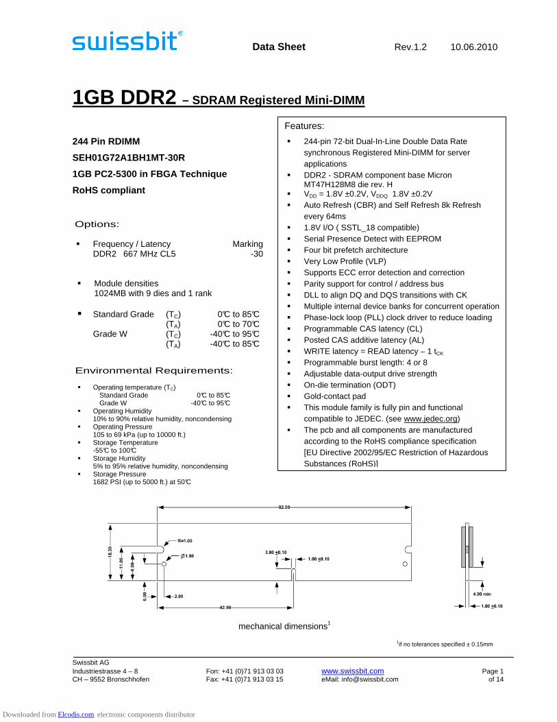
mechanical dimensions1
1if no tolerances specified ± 0.15mm
Downloaded from Elcodis.com electronic components distributor
Data Sheet Rev.1.2 10.06.2010
Swissbit AG Industriestrasse 4 – 8 Fon: +41 (0)71 913 03 03 www.swissbit.com Page 2 CH – 9552 Bronschhofen Fax: +41 (0)71 913 03 15 eMail: [email protected] of 14
This Swissbit module is an industry standard 244-pin 8-byte DDR2 SDRAM mini Dual-In-line Memory Module (miniDIMM) which is organized as x72 high speed CMOS memory arrays. The module uses internally configured quad-bank DDR2 SDRAM devices. The module uses double data rate architecture to achieve high-speed operation. DDR2 SDRAM modules operate from a differential clock (CK and CK#). READ and WRITE accesses to a DDR2 SDRAM module is burst-oriented; accesses start at a selected location and continue for a programmed number of locations in a programmed sequence. The burst length is either four or eight locations. An auto precharge function can be enabled to provide a self-timed row precharge that is initiated at the end of a burst access. The DDR2 SDRAM devices have a multibank architecture which allows a concurrent operation that is providing a high effective bandwidth. A self refresh mode is provided and a power-saving “power-down” mode. All inputs and all full drive-strength outputs are SSTL_18 compatible. The DDR2 SDRAM module uses the serial presence detect (SPD) function implemented via serial EEPROM using the standard I2C protocol. This nonvolatile storage device contains 256 bytes. The first 128 bytes are utilized by the DIMM manufacturer (swissbit) to identify the module type, the module’s organization and several timing parameters. The second 128 bytes are available to the end user.
Module Configuration
Organization DDR2 SDRAMs used Row Addr. Device Bank
Select Col. Addr. Refresh Module Bank Select
128M x 72bit 9 x 128M x 8bit (1Gbit)
14 BA0, BA1, BA2
10 8k S0#
Module Dimensions
in mm
82.0 (long) x 18.30(high) x 4 [max] (thickness) Timing Parameters
Part Number Module Density Transfer Rate Memory clock/Data bit rate Latency
SEH01G72A1BH1MT-30[W]R 1024 MB 5.3 GB/s 3.0ns/667MT/s 5300-555
Pin Name
A0 - A13 Address Inputs
BA0, BA1 Bank Address Inputs
DQ0 – DQ63 Data Input / Output
DM0-DM8 Input Data Mask
RAS# Row Address Strobe
CAS# Column Address Strobe
WE# Write Enable
CKE0 Clock Enable
CK0 Clock Input, positive line
CK0# Clock Input, negative line
DQS0 – DQS17 Data Strobe, positive line
DQS0# - DQS17# Data Strobe, negative line (only used when differential data strobe mode is enabled)
S0# Chip Select
Downloaded from Elcodis.com electronic components distributor
Data Sheet Rev.1.2 10.06.2010
Swissbit AG Industriestrasse 4 – 8 Fon: +41 (0)71 913 03 03 www.swissbit.com Page 3 CH – 9552 Bronschhofen Fax: +41 (0)71 913 03 15 eMail: [email protected] of 14
Reset# Asynchronously forces all registered outputs LOW when RESET# is LOW. This signal can be used during power-up to ensure that CKE is LOW and DQs are High-Z.
PAR_IN Parity bit for the address and control bus.
ERR_OUT Parity error found on the address and control bus.
CB0 – CB7 Check Bits
VDD / VDDQ Supply Voltage (1.8V± 0.1V)
VREF Input / Output Reference
VSS Ground
VDDSPD Serial EEPROM Positive Power Supply
SCL Serial Clock for Presence Detect
SDA Serial Data Out for Presence Detect
SA0 – SA1 Presence Detect Address Inputs
ODT0 On-Die Termination
NC No Connection
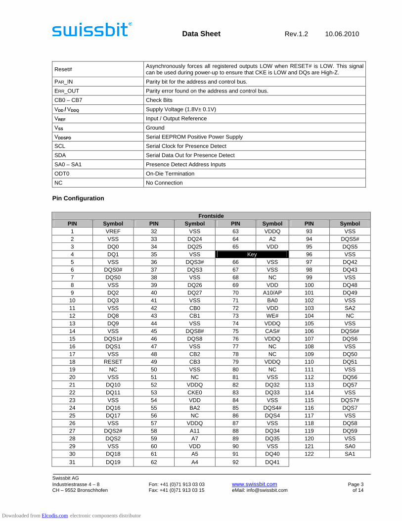
Pin Configuration
Frontside
PIN Symbol PIN Symbol PIN Symbol PIN Symbol 1 VREF 32 VSS 63 VDDQ 93 VSS 2 VSS 33 DQ24 64 A2 94 DQS5# 3 DQ0 34 DQ25 65 VDD 95 DQS5 4 DQ1 35 VSS Key 96 VSS 5 VSS 36 DQS3# 66 VSS 97 DQ42 6 DQS0# 37 DQS3 67 VSS 98 DQ43 7 DQS0 38 VSS 68 NC 99 VSS 8 VSS 39 DQ26 69 VDD 100 DQ48 9 DQ2 40 DQ27 70 A10/AP 101 DQ49
10 DQ3 41 VSS 71 BA0 102 VSS 11 VSS 42 CB0 72 VDD 103 SA2 12 DQ8 43 CB1 73 WE# 104 NC 13 DQ9 44 VSS 74 VDDQ 105 VSS 14 VSS 45 DQS8# 75 CAS# 106 DQS6# 15 DQS1# 46 DQS8 76 VDDQ 107 DQS6 16 DQS1 47 VSS 77 NC 108 VSS 17 VSS 48 CB2 78 NC 109 DQ50 18 RESET 49 CB3 79 VDDQ 110 DQ51 19 NC 50 VSS 80 NC 111 VSS 20 VSS 51 NC 81 VSS 112 DQ56 21 DQ10 52 VDDQ 82 DQ32 113 DQ57 22 DQ11 53 CKE0 83 DQ33 114 VSS 23 VSS 54 VDD 84 VSS 115 DQS7# 24 DQ16 55 BA2 85 DQS4# 116 DQS7 25 DQ17 56 NC 86 DQS4 117 VSS 26 VSS 57 VDDQ 87 VSS 118 DQ58 27 DQS2# 58 A11 88 DQ34 119 DQ59 28 DQS2 59 A7 89 DQ35 120 VSS 29 VSS 60 VDD 90 VSS 121 SA0 30 DQ18 61 A5 91 DQ40 122 SA1
31 DQ19 62 A4 92 DQ41
Downloaded from Elcodis.com electronic components distributor
Data Sheet Rev.1.2 10.06.2010
Swissbit AG Industriestrasse 4 – 8 Fon: +41 (0)71 913 03 03 www.swissbit.com Page 4 CH – 9552 Bronschhofen Fax: +41 (0)71 913 03 15 eMail: [email protected] of 14
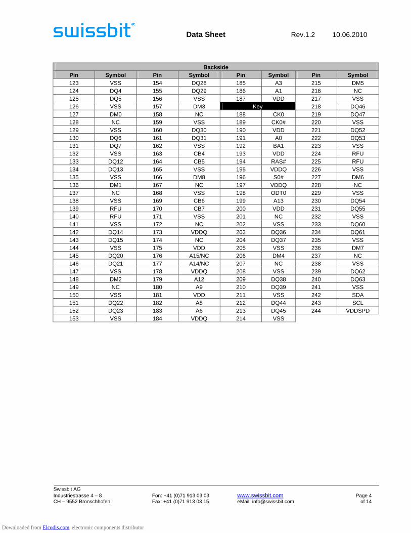
Backside Pin Symbol Pin Symbol Pin Symbol Pin Symbol 123 VSS 154 DQ28 185 A3 215 DM5 124 DQ4 155 DQ29 186 A1 216 NC 125 DQ5 156 VSS 187 VDD 217 VSS 126 VSS 157 DM3 Key 218 DQ46 127 DM0 158 NC 188 CK0 219 DQ47 128 NC 159 VSS 189 CK0# 220 VSS 129 VSS 160 DQ30 190 VDD 221 DQ52 130 DQ6 161 DQ31 191 A0 222 DQ53 131 DQ7 162 VSS 192 BA1 223 VSS 132 VSS 163 CB4 193 VDD 224 RFU 133 DQ12 164 CB5 194 RAS# 225 RFU 134 DQ13 165 VSS 195 VDDQ 226 VSS 135 VSS 166 DM8 196 S0# 227 DM6 136 DM1 167 NC 197 VDDQ 228 NC 137 NC 168 VSS 198 ODT0 229 VSS 138 VSS 169 CB6 199 A13 230 DQ54 139 RFU 170 CB7 200 VDD 231 DQ55 140 RFU 171 VSS 201 NC 232 VSS 141 VSS 172 NC 202 VSS 233 DQ60 142 DQ14 173 VDDQ 203 DQ36 234 DQ61 143 DQ15 174 NC 204 DQ37 235 VSS 144 VSS 175 VDD 205 VSS 236 DM7 145 DQ20 176 A15/NC 206 DM4 237 NC 146 DQ21 177 A14/NC 207 NC 238 VSS 147 VSS 178 VDDQ 208 VSS 239 DQ62 148 DM2 179 A12 209 DQ38 240 DQ63 149 NC 180 A9 210 DQ39 241 VSS 150 VSS 181 VDD 211 VSS 242 SDA 151 DQ22 182 A8 212 DQ44 243 SCL 152 DQ23 183 A6 213 DQ45 244 VDDSPD 153 VSS 184 VDDQ 214 VSS
Downloaded from Elcodis.com electronic components distributor
Data Sheet Rev.1.2 10.06.2010
Swissbit AG Industriestrasse 4 – 8 Fon: +41 (0)71 913 03 03 www.swissbit.com Page 5 CH – 9552 Bronschhofen Fax: +41 (0)71 913 03 15 eMail: [email protected] of 14
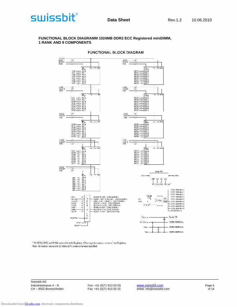
FUNCTIONAL BLOCK DIAGRAMM 1024MB DDR2 ECC Registered miniD IMM, 1 RANK AND 9 COMPONENTS
Downloaded from Elcodis.com electronic components distributor
Data Sheet Rev.1.2 10.06.2010
Swissbit AG Industriestrasse 4 – 8 Fon: +41 (0)71 913 03 03 www.swissbit.com Page 6 CH – 9552 Bronschhofen Fax: +41 (0)71 913 03 15 eMail: [email protected] of 14
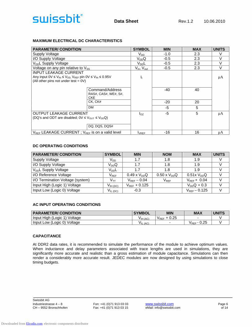
MAXIMUM ELECTRICAL DC CHARACTERISTICS
PARAMETER/ CONDITION SYMBOL MIN MAX UNITS Supply Voltage VDD -1.0 2.3 V I/O Supply Voltage VDDQ -0.5 2.3 V VDDL Supply Voltage VDDL -0.5 2.3 V Voltage on any pin relative to VSS Vin, Vout -0.5 2.3 V INPUT LEAKAGE CURRENT Any input 0V ≤ VIN ≤ VDD, VREF pin 0V ≤ VIN ≤ 0.95V (All other pins not under test = 0V)
Command/Address RAS#, CAS#, WE#, S#, CKE
-40 40
CK, CK# -20 20
DM
II
-5 5
µA
OUTPUT LEAKAGE CURRENT (DQ’s and ODT are disabled; 0V ≤ VOUT ≤ VDDQ) DQ, DQS, DQS#
IOZ -5 5 µA
VREF LEAKAGE CURRENT ; VREF is on a valid level IVREF -16 16 µA DC OPERATING CONDITIONS
PARAMETER/ CONDITION SYMBOL MIN NOM MAX UNITS Supply Voltage VDD 1.7 1.8 1.9 V I/O Supply Voltage VDDQ 1.7 1.8 1.9 V VDDL Supply Voltage VDDL 1.7 1.8 1.9 V I/O Reference Voltage VREF 0.49 x VDDQ 0.50 x VDDQ 0.51x VDDQ V I/O Termination Voltage (system) VTT VREF – 0.04 VREF VREF + 0.04 V Input High (Logic 1) Voltage VIH (DC) VREF + 0.125 VDDQ + 0.3 V Input Low (Logic 0) Voltage VIL (DC) -0.3 VREF – 0.125 V AC INPUT OPERATING CONDITIONS
PARAMETER/ CONDITION SYMBOL MIN MAX UNITS Input High (Logic 1) Voltage VIH (AC) VREF + 0.25 - V Input Low (Logic 0) Voltage VIL (AC) - VREF - 0.25 V CAPACITANCE
At DDR2 data rates, it is recommended to simulate the performance of the module to achieve optimum values. When inductance and delay parameters associated with trace lengths are used in simulations, they are significantly more accurate and realistic than a gross estimation of module capacitance. Simulations can then render a considerably more accurate result. JEDEC modules are now designed by using simulations to close timing budgets.
Downloaded from Elcodis.com electronic components distributor

Data Sheet Rev.1.2 10.06.2010
Swissbit AG Industriestrasse 4 – 8 Fon: +41 (0)71 913 03 03 www.swissbit.com Page 7 CH – 9552 Bronschhofen Fax: +41 (0)71 913 03 15 eMail: [email protected] of 14
IDD Specifications and Conditions (0°C ≤ TCASE ≤ + 85°C V DDQ = +1.8V ± 0.1V, VDD = +1.8V ± 0.1V)
max. Parameter
& Test Condition Symbol
5300-555 Unit
OPERATING CURRENT *) : One device bank Active-Precharge; tRC= tRC (IDD); tCK = tCK (IDD); CKE is HIGH, CS# is HIGH between valid commands; DQ inputs changing once per clock cycle; Address and control inputs changing once every two clock cycles
IDDO 765 mA
OPERATING CURRENT*) : One device bank; Active-Read-Precharge; IOUT = 0mA; BL = 4, CL = CL (IDD), AL = 0; tCK = tCK (IDD), tRC= tRC (IDD), tRAS = tRAS MIN (IDD), tRCD = tRCD (IDD); CKE is HIGH, CS# is HIGH between valid commands; Address inputs changing once every two clock cycles; Data Pattern is same as IDD4W
IDD1 900 mA
PRECHARGE POWER-DOWN CURRENT: All device banks idle; Power-down mode; tCK = tCK (IDD); CKE is LOW; All Control and Address bus inputs are not changing; DQ’s are floating at VREF
IDD2P 63 mA
PRECHARGE QUIET STANDBY CURRENT: All device banks idle; tCK = tCK (IDD); CKE is HIGH, CS# is HIGH; All Control and Address bus inputs are not changing; DQ’s are floating at VREF
IDD2Q 360 mA
PRECHARGE STANDBY CURRENT: All device banks idle; tCK = tCK (IDD); CKE is HIGH, CS# is HIGH; All other Control and Address bus inputs are changing once every two clock cycles; DQ inputs changing once per clock cycle
IDD2N 360 mA
Fast PDN Exit MR[12] = 0
270 ACTIVE POWER-DOWN CURRENT: All device banks open; tCK = tCK
(IDD); CKE is LOW; All Control and Address bus inputs are not changing; DQ’s are floating at VREF
Slow PDN Exit MR[12] = 1
IDD3P
90
mA
ACTIVE STANDBY CURRENT: All device banks open; tCK = tCK (IDD), tRAS = tRAS MAX (IDD), tRP = tRP (IDD); CKE is HIGH, CS# is HIGH between valid commands; All other Control and Address bus inputs are changing once every two clock cycles; DQ inputs changing once per clock cycle
IDD3N 495 mA
OPERATING READ CURRENT*) : All device banks open, Continuous burst reads; One module rank active; IOUT = 0mA; BL = 4, CL = CL (IDD), AL = 0; tCK = tCK (IDD), tRAS = tRAS MAX (IDD), tRP = tRP (IDD); CKE is HIGH, CS# is HIGH between valid commands; Address bus inputs are changing once every two clock cycles; DQ inputs changing once per clock cycle
IDD4R 1215 mA
Downloaded from Elcodis.com electronic components distributor

Data Sheet Rev.1.2 10.06.2010
Swissbit AG Industriestrasse 4 – 8 Fon: +41 (0)71 913 03 03 www.swissbit.com Page 8 CH – 9552 Bronschhofen Fax: +41 (0)71 913 03 15 eMail: [email protected] of 14
Max. Parameter
& Test Condition Symbol
5300-555 Unit
OPERATING WRITE CURRENT*) : All device banks open, Continuous burst writes; One module rank active; BL = 4, CL = CL (IDD), AL = 0; tCK = tCK (IDD), tRAS = tRAS MAX (IDD), tRP = tRP (IDD); CKE is HIGH, CS# is HIGH between valid commands; Address bus inputs are changing once every two clock cycles; DQ inputs changing once per clock cycle
IDD4W 1215 mA
BURST REFRESH CURRENT: tCK = tCK (IDD); refresh command at every tRFC (IDD) interval, CKE is HIGH, CS# is HIGH between valid commands; All other Control and Address bus inputs are changing once every two clock cycles; DQ inputs changing once per clock cycle
IDD5 1935 mA
SELF REFRESH CURRENT: CK and CK# at 0V; CKE ≤ 0.2V; All other Control and Address bus inputs are floating at VREF; DQ’s are floating at VREF
IDD6 63 mA
OPERATING CURRENT*) : Four device bank interleaving READs, IOUT = 0mA; BL = 4, CL = CL (IDD), AL = tRCD (IDD) – 1 x tCK (IDD); tCK = tCK (IDD), tRC = tRC (IDD), tRRD = tRRD (IDD), tRCD = tRCD (IDD); CKE is HIGH, CS# is HIGH between valid commands; Address bus inputs are not changing during DESELECT; DQ inputs changing once per clock cycle
IDD7 2520 mA
*) Value calculated as one module rank in this oper ating condition, and all other module ranks in IDD2 P (CKE LOW) mode.
TIMING VALUES USED FOR IDD MEASUREMENT
IDD MEASUREMENT CONDITIONS SYMBOL 5300-555 Unit CL (IDD) 5 tCK tRCD (IDD) 15 ns tRC (IDD) 60 ns tRRD (IDD) 7.5 ns tCK (IDD) 3.0 ns tRAS MIN (IDD) 45 ns tRAS MAX (IDD) 70,000 ns
tRP (IDD) 15 ns tRFC (IDD) 105 ns
Downloaded from Elcodis.com electronic components distributor
Data Sheet Rev.1.2 10.06.2010
Swissbit AG Industriestrasse 4 – 8 Fon: +41 (0)71 913 03 03 www.swissbit.com Page 9 CH – 9552 Bronschhofen Fax: +41 (0)71 913 03 15 eMail: [email protected] of 14
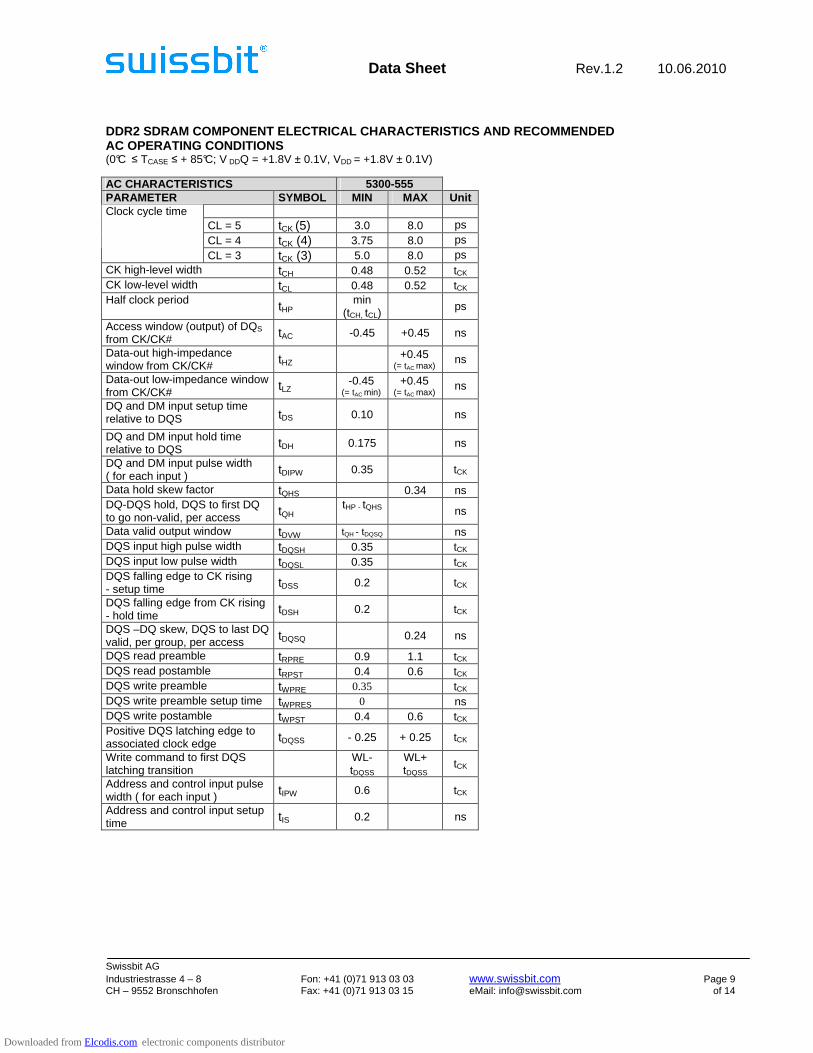
DDR2 SDRAM COMPONENT ELECTRICAL CHARACTERISTICS AND RECO MMENDED AC OPERATING CONDITIONS (0°C ≤ TCASE ≤ + 85°C; V DDQ = +1.8V ± 0.1V, VDD = +1.8V ± 0.1V)
AC CHARACTERISTICS 5300-555 PARAMETER SYMBOL MIN MAX Unit
CL = 5 tCK (5) 3.0 8.0 ps CL = 4 tCK (4) 3.75 8.0 ps
Clock cycle time
CL = 3 tCK (3) 5.0 8.0 ps CK high-level width tCH 0.48 0.52 tCK CK low-level width tCL 0.48 0.52 tCK Half clock period tHP min
(tCH, tCL) ps
Access window (output) of DQS from CK/CK#
tAC -0.45 +0.45 ns
Data-out high-impedance window from CK/CK# tHZ +0.45
(= tAC max) ns
Data-out low-impedance window from CK/CK# tLZ -0.45
(= tAC min) +0.45
(= tAC max) ns
DQ and DM input setup time relative to DQS tDS 0.10 ns
DQ and DM input hold time relative to DQS tDH 0.175 ns
DQ and DM input pulse width ( for each input ) tDIPW 0.35 tCK
Data hold skew factor tQHS 0.34 ns DQ-DQS hold, DQS to first DQ to go non-valid, per access tQH tHP - tQHS
ns
Data valid output window tDVW tQH - tDQSQ ns DQS input high pulse width tDQSH 0.35 tCK DQS input low pulse width tDQSL 0.35 tCK DQS falling edge to CK rising - setup time tDSS 0.2 tCK
DQS falling edge from CK rising - hold time tDSH 0.2 tCK
DQS –DQ skew, DQS to last DQ valid, per group, per access tDQSQ 0.24 ns
DQS read preamble tRPRE 0.9 1.1 tCK DQS read postamble tRPST 0.4 0.6 tCK DQS write preamble tWPRE 0.35 tCK DQS write preamble setup time tWPRES 0 ns DQS write postamble tWPST 0.4 0.6 tCK Positive DQS latching edge to associated clock edge tDQSS - 0.25 + 0.25 tCK
Write command to first DQS latching transition
WL- tDQSS
WL+ tDQSS tCK
Address and control input pulse width ( for each input ) tIPW 0.6 tCK
Address and control input setup time tIS 0.2 ns
Downloaded from Elcodis.com electronic components distributor
Data Sheet Rev.1.2 10.06.2010
Swissbit AG Industriestrasse 4 – 8 Fon: +41 (0)71 913 03 03 www.swissbit.com Page 10 CH – 9552 Bronschhofen Fax: +41 (0)71 913 03 15 eMail: [email protected] of 14
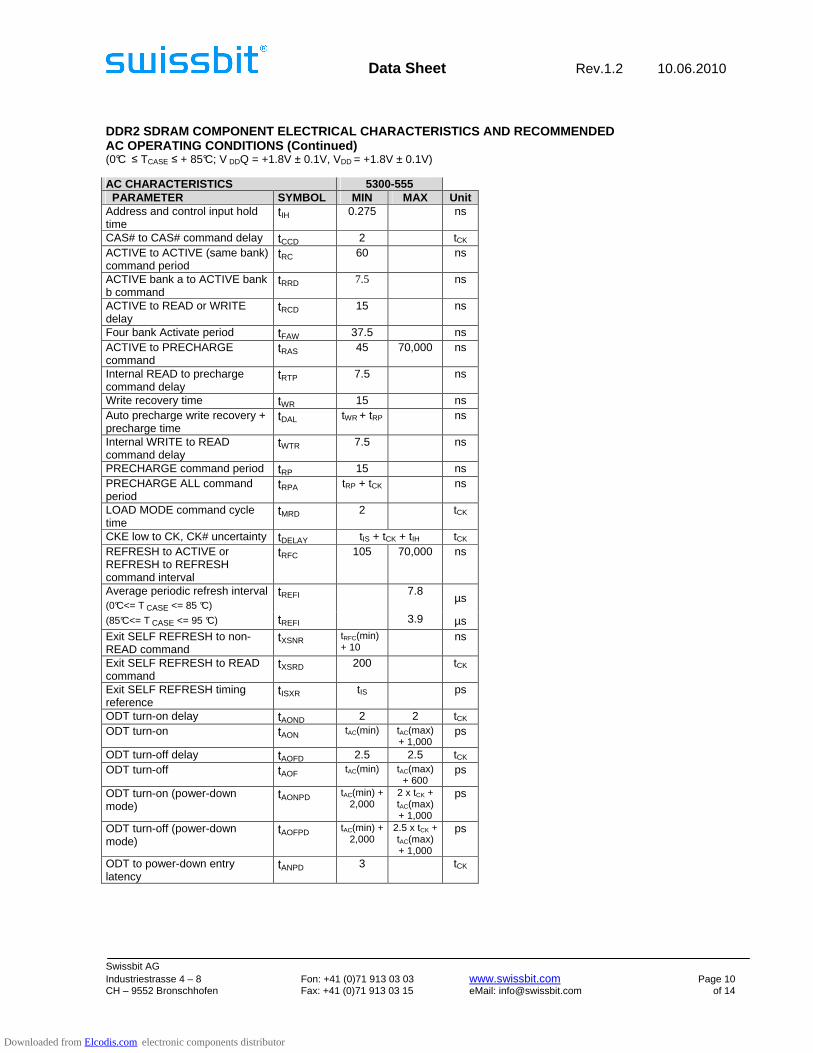
DDR2 SDRAM COMPONENT ELECTRICAL CHARACTERISTICS AND RECO MMENDED AC OPERATING CONDITIONS (Continued) (0°C ≤ TCASE ≤ + 85°C; V DDQ = +1.8V ± 0.1V, VDD = +1.8V ± 0.1V)
AC CHARACTERISTICS 5300-555 PARAMETER SYMBOL MIN MAX Unit Address and control input hold time
tIH 0.275 ns
CAS# to CAS# command delay tCCD 2 tCK
ACTIVE to ACTIVE (same bank) command period
tRC 60 ns
ACTIVE bank a to ACTIVE bank b command
tRRD 7.5 ns
ACTIVE to READ or WRITE delay
tRCD 15 ns
Four bank Activate period tFAW 37.5 ns ACTIVE to PRECHARGE command
tRAS 45 70,000 ns
Internal READ to precharge command delay
tRTP 7.5 ns
Write recovery time tWR 15 ns Auto precharge write recovery + precharge time
tDAL tWR + tRP
ns
Internal WRITE to READ command delay
tWTR 7.5 ns
PRECHARGE command period tRP 15 ns PRECHARGE ALL command period
tRPA tRP + tCK ns
LOAD MODE command cycle time
tMRD 2 tCK
CKE low to CK, CK# uncertainty tDELAY tIS + tCK + tIH tCK REFRESH to ACTIVE or REFRESH to REFRESH command interval
tRFC 105 70,000 ns
Average periodic refresh interval (0°C<= T CASE <= 85 °C)
tREFI 7.8 µs
(85°C<= T CASE <= 95 °C) tREFI 3.9 µs Exit SELF REFRESH to non-READ command
tXSNR tRFC(min) + 10
ns
Exit SELF REFRESH to READ command
tXSRD 200 tCK
Exit SELF REFRESH timing reference
tISXR tIS ps
ODT turn-on delay tAOND 2 2 tCK ODT turn-on tAON tAC(min) tAC(max)
+ 1,000 ps
ODT turn-off delay tAOFD 2.5 2.5 tCK ODT turn-off tAOF tAC(min) tAC(max)
+ 600 ps
ODT turn-on (power-down mode)
tAONPD tAC(min) + 2,000
2 x tCK + tAC(max) + 1,000
ps
ODT turn-off (power-down mode)
tAOFPD tAC(min) + 2,000
2.5 x tCK + tAC(max) + 1,000
ps
ODT to power-down entry latency
tANPD 3 tCK
Downloaded from Elcodis.com electronic components distributor

Data Sheet Rev.1.2 10.06.2010
Swissbit AG Industriestrasse 4 – 8 Fon: +41 (0)71 913 03 03 www.swissbit.com Page 11 CH – 9552 Bronschhofen Fax: +41 (0)71 913 03 15 eMail: [email protected] of 14
DDR2 SDRAM COMPONENT ELECTRICAL CHARACTERISTICS AND RECO MMENDED AC OPERATING CONDITIONS (Continued) (0°C ≤ TCASE ≤ + 85°C; V DDQ = +1.8V ± 0.1V, VDD = +1.8V ± 0.1V)
AC CHARACTERISTICS 5300-555 PARAMETER SYMBOL MIN MAX Unit ODT power-down exit latency tAXPD 8 tCK ODT enable from MRS command
TMOD 12 ns
Exit active power-down to READ command, MR [bit 12 = 0]
tXARD 2 tCK
Exit active power-down to READ command, MR [bit 12 = 1]
tXARDS 7 - AL tCK
Exit precharge power-down to any non-READ command
tXP 2 tCK
CKE minimum high/low time tCKE 3 tCK
Register Specifications Parameter Symbol Pins Conditions Min Max Units
DC high-level input voltage VIH(DC)
Address, control, command
SSTL_18 VREF(DC) + 125 VDDQ + 250 mV
DC low-level input voltage VIL(DC)
Address, control, command
SSTL_18 0 VREF(DC) - 125 mV
AC high-level input voltage VIH(AC)
Address, control, command
SSTL_18 VREF(DC) + 250 VDD mV
AC low-level input voltage VIL(AC)
Address, control, command
SSTL_18 0 VREF(DC) - 250 mV
Output high voltage VOH Parity output LVCMOS 1.2 - V
Output low voltage VOL Parity output LVCMOS - 0.5 V
Input current II All pins VI = VDDQ or VSSQ -5 +5 µA Static standby IDD All pins RESET# = VSSQ (IO = 0) - 100 µA
Static operating IDD All pins RESET# = VSSQ;
VI = VIH(AC) or VIL(DC) IO = 0
- 40 mA
Dynamic operating (clock tree) IDDD n/a
RESET# = VDD, VI = VIH(AC) or VIL(AC), IO = 0; CK and CK#
switching 50% duty cycle - Varies by
manufacturer µA
Dynamic operating (per each input) IDDD n/a
RESET# = VDD, VI = VIH(AC) or VIL(AC), IO = 0; CK and CK# switching 50% duty cycle; One data input switching at
tCK/2, 50% duty cycle
- Varies by manufacturer µA
Input capacitance (per device, per pin) CI Data VI = VREF ±250mV;
VDDQ = 1.8V 2.5 3.5 pF
Input capacitance (per device, per pin) CI RESET# VI = VDDQ or VSSQ - Varies by
manufacturer pF
Notes: 1. Timing and switching specifications for the register listed above are critical for proper operation of the DDR2
SDRAM registered DIMMs. These are meant to be a subset of the parameters for the specific device used on the module. Detailed information for this register is available in JEDEC standard JESD82.
Downloaded from Elcodis.com electronic components distributor
Data Sheet Rev.1.2 10.06.2010
Swissbit AG Industriestrasse 4 – 8 Fon: +41 (0)71 913 03 03 www.swissbit.com Page 12 CH – 9552 Bronschhofen Fax: +41 (0)71 913 03 15 eMail: [email protected] of 14
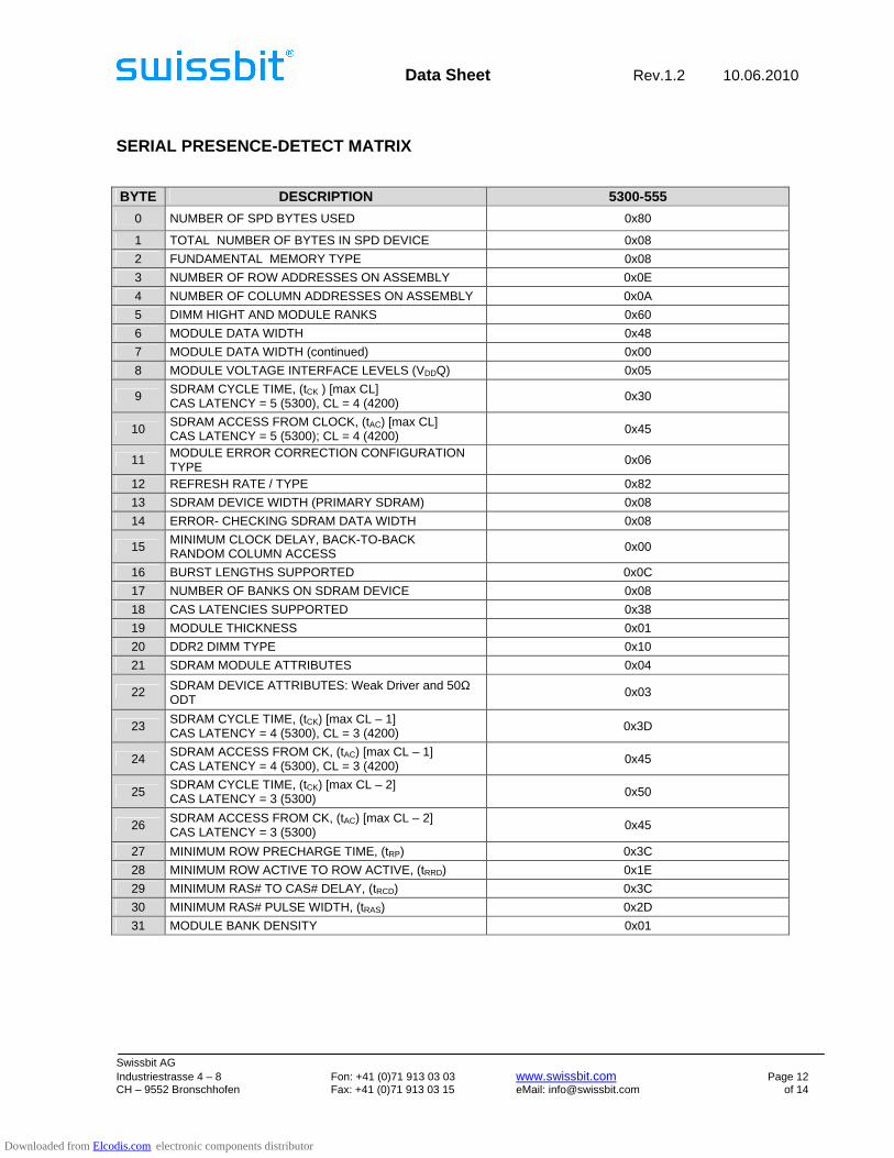
SERIAL PRESENCE-DETECT MATRIX BYTE DESCRIPTION 5300-555
0 NUMBER OF SPD BYTES USED 0x80
1 TOTAL NUMBER OF BYTES IN SPD DEVICE 0x08
2 FUNDAMENTAL MEMORY TYPE 0x08
3 NUMBER OF ROW ADDRESSES ON ASSEMBLY 0x0E
4 NUMBER OF COLUMN ADDRESSES ON ASSEMBLY 0x0A
5 DIMM HIGHT AND MODULE RANKS 0x60
6 MODULE DATA WIDTH 0x48
7 MODULE DATA WIDTH (continued) 0x00
8 MODULE VOLTAGE INTERFACE LEVELS (VDDQ) 0x05
9 SDRAM CYCLE TIME, (tCK ) [max CL] CAS LATENCY = 5 (5300), CL = 4 (4200) 0x30
10 SDRAM ACCESS FROM CLOCK, (tAC) [max CL] CAS LATENCY = 5 (5300); CL = 4 (4200) 0x45
11 MODULE ERROR CORRECTION CONFIGURATION TYPE
0x06
12 REFRESH RATE / TYPE 0x82
13 SDRAM DEVICE WIDTH (PRIMARY SDRAM) 0x08
14 ERROR- CHECKING SDRAM DATA WIDTH 0x08
15 MINIMUM CLOCK DELAY, BACK-TO-BACK RANDOM COLUMN ACCESS 0x00
16 BURST LENGTHS SUPPORTED 0x0C
17 NUMBER OF BANKS ON SDRAM DEVICE 0x08
18 CAS LATENCIES SUPPORTED 0x38
19 MODULE THICKNESS 0x01
20 DDR2 DIMM TYPE 0x10
21 SDRAM MODULE ATTRIBUTES 0x04
22 SDRAM DEVICE ATTRIBUTES: Weak Driver and 50Ω ODT
0x03
23 SDRAM CYCLE TIME, (tCK) [max CL – 1] CAS LATENCY = 4 (5300), CL = 3 (4200) 0x3D
24 SDRAM ACCESS FROM CK, (tAC) [max CL – 1] CAS LATENCY = 4 (5300), CL = 3 (4200) 0x45
25 SDRAM CYCLE TIME, (tCK) [max CL – 2] CAS LATENCY = 3 (5300) 0x50
26 SDRAM ACCESS FROM CK, (tAC) [max CL – 2] CAS LATENCY = 3 (5300) 0x45
27 MINIMUM ROW PRECHARGE TIME, (tRP) 0x3C
28 MINIMUM ROW ACTIVE TO ROW ACTIVE, (tRRD) 0x1E
29 MINIMUM RAS# TO CAS# DELAY, (tRCD) 0x3C
30 MINIMUM RAS# PULSE WIDTH, (tRAS) 0x2D
31 MODULE BANK DENSITY 0x01
Downloaded from Elcodis.com electronic components distributor
Data Sheet Rev.1.2 10.06.2010
Swissbit AG Industriestrasse 4 – 8 Fon: +41 (0)71 913 03 03 www.swissbit.com Page 13 CH – 9552 Bronschhofen Fax: +41 (0)71 913 03 15 eMail: [email protected] of 14
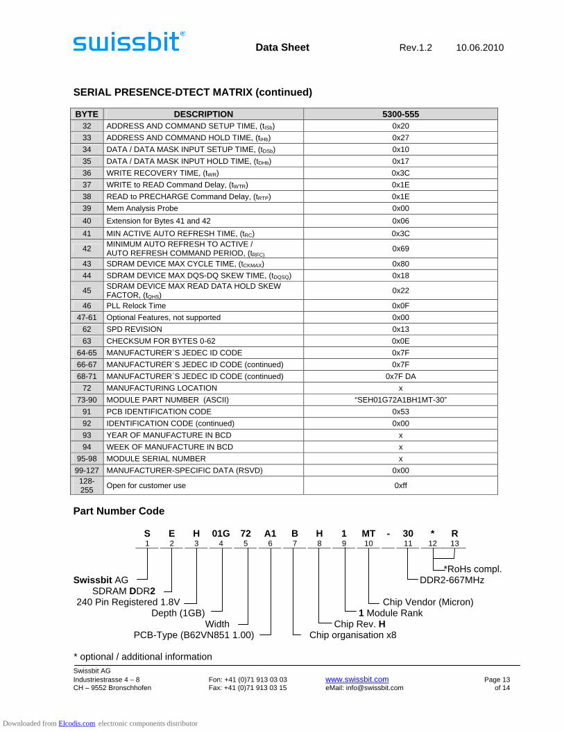
SERIAL PRESENCE-DTECT MATRIX (continued) BYTE DESCRIPTION 5300-555
32 ADDRESS AND COMMAND SETUP TIME, (tISb) 0x20
33 ADDRESS AND COMMAND HOLD TIME, (tIHb) 0x27
34 DATA / DATA MASK INPUT SETUP TIME, (tDSb) 0x10
35 DATA / DATA MASK INPUT HOLD TIME, (tDHb) 0x17
36 WRITE RECOVERY TIME, (tWR) 0x3C
37 WRITE to READ Command Delay, (tWTR) 0x1E
38 READ to PRECHARGE Command Delay, (tRTP) 0x1E
39 Mem Analysis Probe 0x00
40 Extension for Bytes 41 and 42 0x06
41 MIN ACTIVE AUTO REFRESH TIME, (tRC) 0x3C
42 MINIMUM AUTO REFRESH TO ACTIVE / AUTO REFRESH COMMAND PERIOD, (tRFC)
0x69
43 SDRAM DEVICE MAX CYCLE TIME, (tCKMAX) 0x80
44 SDRAM DEVICE MAX DQS-DQ SKEW TIME, (tDQSQ) 0x18
45 SDRAM DEVICE MAX READ DATA HOLD SKEW FACTOR, (tQHS) 0x22
46 PLL Relock Time 0x0F
47-61 Optional Features, not supported 0x00
62 SPD REVISION 0x13
63 CHECKSUM FOR BYTES 0-62 0x0E
64-65 MANUFACTURER`S JEDEC ID CODE 0x7F
66-67 MANUFACTURER`S JEDEC ID CODE (continued) 0x7F
68-71 MANUFACTURER`S JEDEC ID CODE (continued) 0x7F DA
72 MANUFACTURING LOCATION x
73-90 MODULE PART NUMBER (ASCII) “SEH01G72A1BH1MT-30”
91 PCB IDENTIFICATION CODE 0x53
92 IDENTIFICATION CODE (continued) 0x00
93 YEAR OF MANUFACTURE IN BCD x
94 WEEK OF MANUFACTURE IN BCD x
95-98 MODULE SERIAL NUMBER x
99-127 MANUFACTURER-SPECIFIC DATA (RSVD) 0x00 128-255
Open for customer use 0xff
Part Number Code
S E H 01G 72 A1 B H 1 MT - 30 * R 1 2 3 4 5 6 7 8 9 10 11 12 13
*RoHs compl. Swissbit AG DDR2-667MHz
SDRAM DDR2 240 Pin Registered 1.8V Chip Vendor (Micron)
Depth (1GB) 1 Module Rank Width Chip Rev. H
PCB-Type (B62VN851 1.00) Chip organisation x8
* optional / additional information
Downloaded from Elcodis.com electronic components distributor
Data Sheet Rev.1.2 10.06.2010
Swissbit AG Industriestrasse 4 – 8 Fon: +41 (0)71 913 03 03 www.swissbit.com Page 14 CH – 9552 Bronschhofen Fax: +41 (0)71 913 03 15 eMail: [email protected] of 14
Locations
Swissbit AG Industriestrasse 4 – 8 CH – 9552 Bronschhofen Switzerland Phone: +41 (0)71 913 03 03 Fax: +41 (0)71 913 03 15 _____________________________ Swissbit Germany GmbH Wolfener Strasse 36 D – 12681 Berlin Germany Phone: +49 (0)30 93 69 54 – 0 Fax: +49 (0)30 93 69 54 – 55 _____________________________ Swissbit NA, Inc. 14 Willett Avenue, Suite 301A Port Chester, NY 10573 USA Phone: +1 914 935 1400 Fax: +1 914 935 9865 _____________________________ Swissbit NA, Inc. 3913 Todd Lane, Suite – 307 Austin, TX 78744 USA Phone: +1 512 302 9001 Fax: +1 512 302 4808 _____________________________ Swissbit Japan, Inc. 3F Core Koenji, 2-1-24 Koenji-Kita, Suginami-Ku, Tokyo 166-0002 Japan Phone: +81 3 5356 3511 Fax: +81 3 5356 3512
Downloaded from Elcodis.com electronic components distributor