Embed Size (px)
Citation preview
1V SUPPLY CMOS DEMUX FOR 40-GB/S OPTICAL COMMUNICATION SYSTEMS
Bangli Liang, Tad Kwasniewski, Dianyong Chen, Bo Wang, Dezhong Cheng
Department of Electronics, Carleton University, 1125 Colonel By Drive, Ottawa, ON, K1S 5B6, Canada
ABSTRACT A 1V supply 1:2 demultiplexer (DEMUX) based on 0.13µm CMOS technology is presented. It is designed for 40-Gb/s optical communication systems. This DEMUX achieved by a pair of master-slave flip-flops (MS-FFs) with opposite clock can operate at 40-Gb/s and beyond. Fully differential current mode logic (CML) is adopted to improve the bit rate of non-return-to-zero (NRZ) data stream and to suppress common mode disturbances. Output buffers for two outputs are employed to drive the external 50Ω loads. On-chip shunt peaking (SP) inductors are used to boost the bandwidth. Stacked current source combined with low VT and Regular VT NMOS is used so that the proposed DEMUX has good immunity against possible process, voltage and temperature (PVT) variations. This DEMUX IC dissipates a total current of 25mA under a 1V supply and consumes a chip area of 0.54mm2 with bonding pads.
1. INTRODUCTION
Current serial data communication systems operate at bit rates between 10- and 40-Gb/s. Today’s communication ICs are mainly implemented in GaAs, InP, or SiGe bipolar technologies. Several high-speed chips in standard CMOS technologies are reported in [1]-[3], which confirm CMOS to be a viable alternative and a very economical approach for broadband circuit design. As a key block in data communication systems, current CMOS DEMUXs already achieve bitrates higher than 30-Gb/s [1]-[3]. In this work, a 40-Gb/s 1:2 DEMUX in IBM 0.13µm CMOS technology is presented. The manufactured nMOS transistors have a fT of 100 GHz. All subcircuits of this DEMUX use CML with differential signals. Compared to conventional static CMOS logic, CML circuits employ reduced internal voltage swings, which is essential for high switching speeds [4]. To reach the speed of 40-Gb/s, the DEMUX uses shunt peaking inductors to boost circuit bandwidth. Stacked current source is employed to increase manufactureability and immunity against PVT variations. Low VT transistors are used in core circuit to reduce supply voltage and power dissipation. Additionally, aspect ratio of transistors in data path and clock path and DC bias are optimized to maximize the effective fT and minimize the required supply voltage and power dissipation.
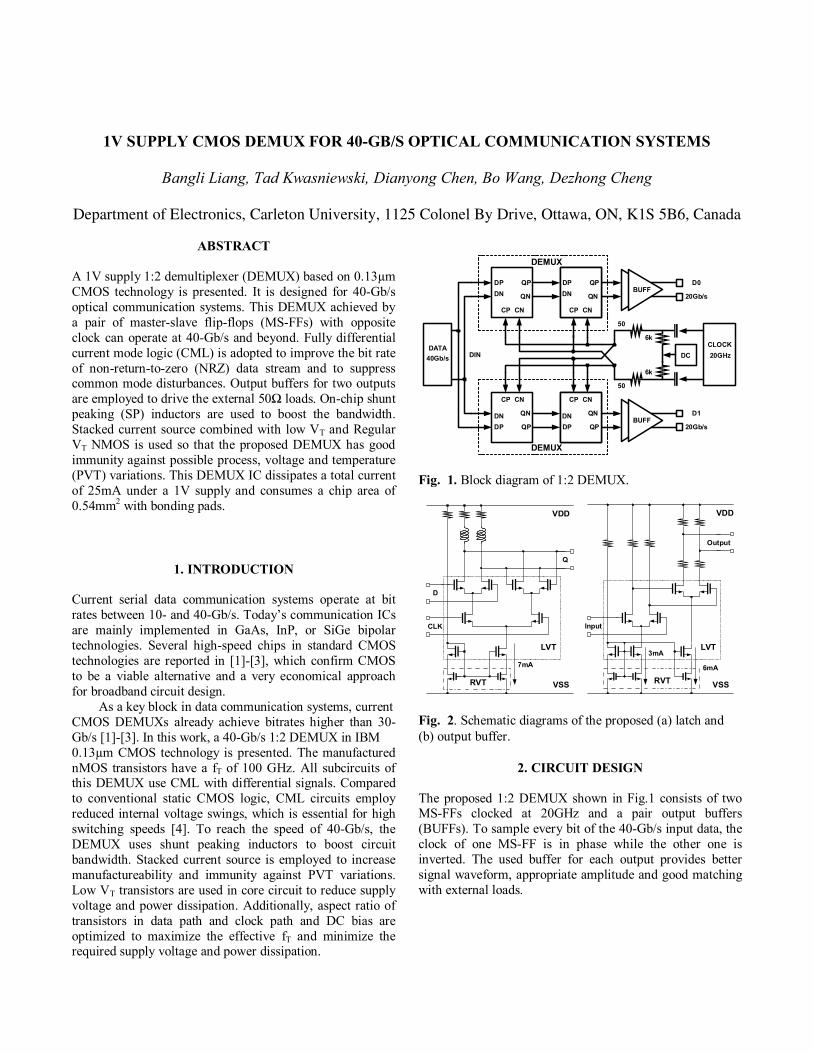
DATA
DPDN
QP
QN
CP CN
DPDN
QP
QN
CP CN
DEMUX
DPDN
QP
QN
CP CN
DPDN
QP
QN
CP CN
DEMUX
DC
BUFF
BUFF
CLOCK
50
50
6k
6k
D0
D1
DIN 20GHz40Gb/s
20Gb/s
20Gb/s
Fig. 1. Block diagram of 1:2 DEMUX.
VDD
D
Q
CLK
LVT
RVT
7mA
VSS
VDD
Input
Output
LVT
RVT
3mA
VSS
6mA
Fig. 2. Schematic diagrams of the proposed (a) latch and (b) output buffer.
2. CIRCUIT DESIGN The proposed 1:2 DEMUX shown in Fig.1 consists of two MS-FFs clocked at 20GHz and a pair output buffers (BUFFs). To sample every bit of the 40-Gb/s input data, the clock of one MS-FF is in phase while the other one is inverted. The used buffer for each output provides better signal waveform, appropriate amplitude and good matching with external loads.
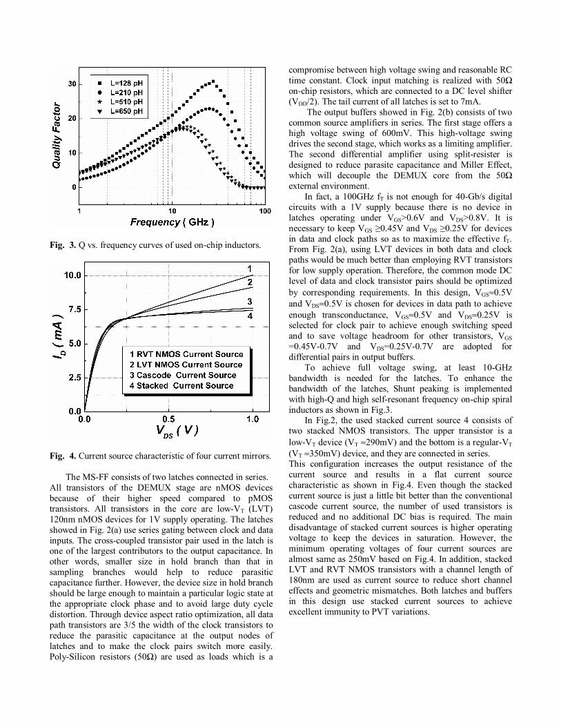
Fig. 3. Q vs. frequency curves of used on-chip inductors.
Fig. 4. Current source characteristic of four current mirrors.
The MS-FF consists of two latches connected in series. All transistors of the DEMUX stage are nMOS devices because of their higher speed compared to pMOS transistors. All transistors in the core are low-VT (LVT) 120nm nMOS devices for 1V supply operating. The latches showed in Fig. 2(a) use series gating between clock and data inputs. The cross-coupled transistor pair used in the latch is one of the largest contributors to the output capacitance. In other words, smaller size in hold branch than that in sampling branches would help to reduce parasitic capacitance further. However, the device size in hold branch should be large enough to maintain a particular logic state at the appropriate clock phase and to avoid large duty cycle distortion. Through device aspect ratio optimization, all data path transistors are 3/5 the width of the clock transistors to reduce the parasitic capacitance at the output nodes of latches and to make the clock pairs switch more easily. Poly-Silicon resistors (50Ω) are used as loads which is a
compromise between high voltage swing and reasonable RC time constant. Clock input matching is realized with 50Ω on-chip resistors, which are connected to a DC level shifter (VDD/2). The tail current of all latches is set to 7mA. The output buffers showed in Fig. 2(b) consists of two common source amplifiers in series. The first stage offers a high voltage swing of 600mV. This high-voltage swing drives the second stage, which works as a limiting amplifier. The second differential amplifier using split-resister is designed to reduce parasite capacitance and Miller Effect, which will decouple the DEMUX core from the 50Ω external environment. In fact, a 100GHz fT is not enough for 40-Gb/s digital circuits with a 1V supply because there is no device in latches operating under VGS>0.6V and VDS>0.8V. It is necessary to keep VGS ≥0.45V and VDS ≥0.25V for devices in data and clock paths so as to maximize the effective fT. From Fig. 2(a), using LVT devices in both data and clock paths would be much better than employing RVT transistors for low supply operation. Therefore, the common mode DC level of data and clock transistor pairs should be optimized by corresponding requirements. In this design, VGS≈0.5V and VDS≈0.5V is chosen for devices in data path to achieve enough transconductance, VGS≈0.5V and VDS≈0.25V is selected for clock pair to achieve enough switching speed and to save voltage headroom for other transistors, VGS =0.45V-0.7V and VDS=0.25V-0.7V are adopted for differential pairs in output buffers. To achieve full voltage swing, at least 10-GHz bandwidth is needed for the latches. To enhance the bandwidth of the latches, Shunt peaking is implemented with high-Q and high self-resonant frequency on-chip spiral inductors as shown in Fig.3. In Fig.2, the used stacked current source 4 consists of two stacked NMOS transistors. The upper transistor is a low-VT device (VT ≈290mV) and the bottom is a regular-VT (VT ≈350mV) device, and they are connected in series. This configuration increases the output resistance of the current source and results in a flat current source characteristic as shown in Fig.4. Even though the stacked current source is just a little bit better than the conventional cascode current source, the number of used transistors is reduced and no additional DC bias is required. The main disadvantage of stacked current sources is higher operating voltage to keep the devices in saturation. However, the minimum operating voltages of four current sources are almost same as 250mV based on Fig.4. In addition, stacked LVT and RVT NMOS transistors with a channel length of 180nm are used as current source to reduce short channel effects and geometric mismatches. Both latches and buffers in this design use stacked current sources to achieve excellent immunity to PVT variations.
(a) (b)
(c) (d)
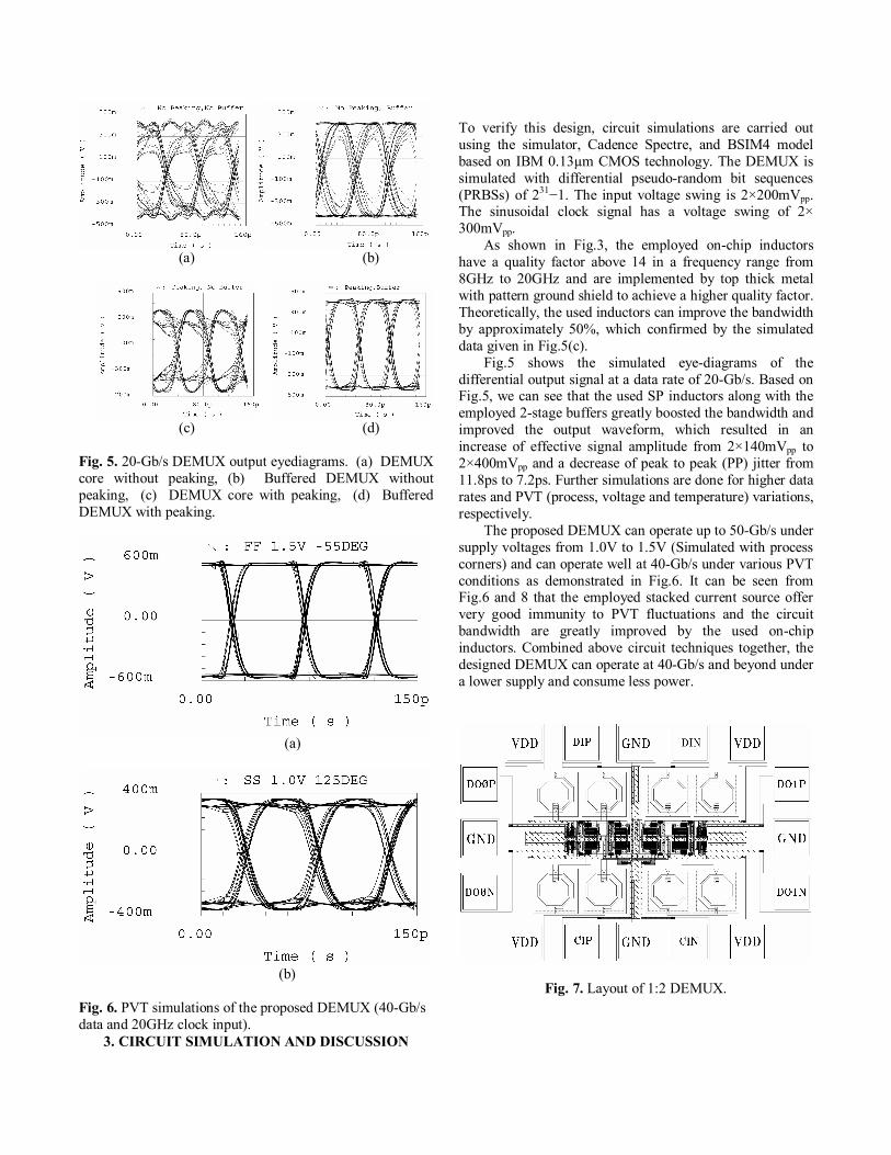
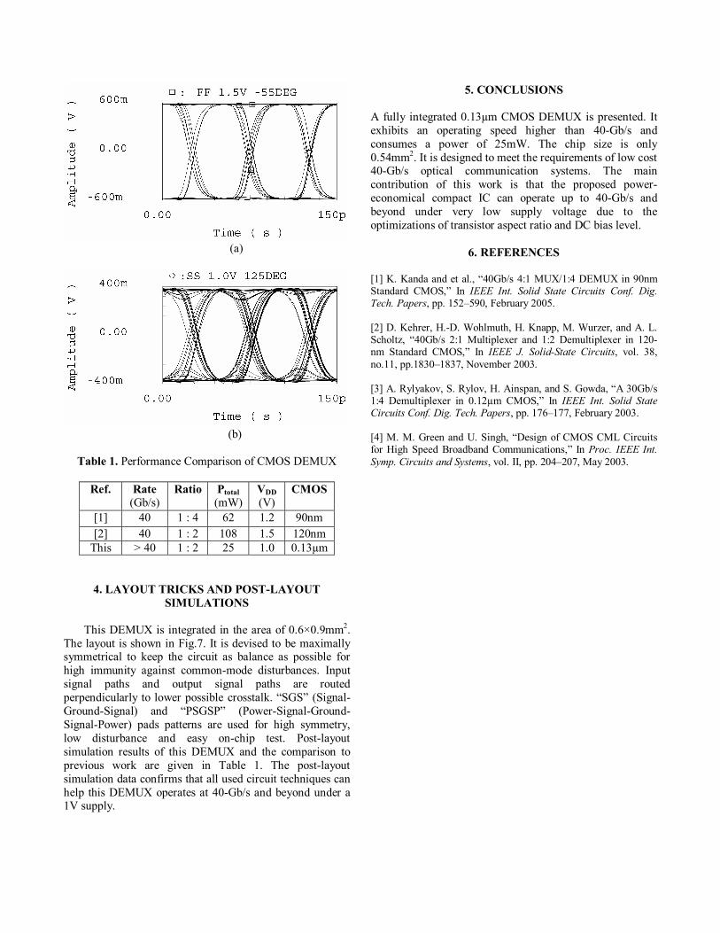
Fig. 5. 20-Gb/s DEMUX output eyediagrams. (a) DEMUX core without peaking, (b) Buffered DEMUX without peaking, (c) DEMUX core with peaking, (d) Buffered DEMUX with peaking.
(a)
(b)
Fig. 6. PVT simulations of the proposed DEMUX (40-Gb/s data and 20GHz clock input).
3. CIRCUIT SIMULATION AND DISCUSSION
To verify this design, circuit simulations are carried out using the simulator, Cadence Spectre, and BSIM4 model based on IBM 0.13µm CMOS technology. The DEMUX is simulated with differential pseudo-random bit sequences (PRBSs) of 231−1. The input voltage swing is 2×200mVpp. The sinusoidal clock signal has a voltage swing of 2× 300mVpp. As shown in Fig.3, the employed on-chip inductors have a quality factor above 14 in a frequency range from 8GHz to 20GHz and are implemented by top thick metal with pattern ground shield to achieve a higher quality factor. Theoretically, the used inductors can improve the bandwidth by approximately 50%, which confirmed by the simulated data given in Fig.5(c). Fig.5 shows the simulated eye-diagrams of the differential output signal at a data rate of 20-Gb/s. Based on Fig.5, we can see that the used SP inductors along with the employed 2-stage buffers greatly boosted the bandwidth and improved the output waveform, which resulted in an increase of effective signal amplitude from 2×140mVpp to 2×400mVpp and a decrease of peak to peak (PP) jitter from 11.8ps to 7.2ps. Further simulations are done for higher data rates and PVT (process, voltage and temperature) variations, respectively. The proposed DEMUX can operate up to 50-Gb/s under supply voltages from 1.0V to 1.5V (Simulated with process corners) and can operate well at 40-Gb/s under various PVT conditions as demonstrated in Fig.6. It can be seen from Fig.6 and 8 that the employed stacked current source offer very good immunity to PVT fluctuations and the circuit bandwidth are greatly improved by the used on-chip inductors. Combined above circuit techniques together, the designed DEMUX can operate at 40-Gb/s and beyond under a lower supply and consume less power.
Fig. 7. Layout of 1:2 DEMUX.
(a)
(b)
Table 1. Performance Comparison of CMOS DEMUX
Ref.
Rate
(Gb/s) Ratio
Ptotal (mW)
VDD (V)
CMOS
[1] 40 1 : 4 62 1.2 90nm [2] 40 1 : 2 108 1.5 120nm
This > 40 1 : 2 25 1.0 0.13µm
4. LAYOUT TRICKS AND POST-LAYOUT
SIMULATIONS This DEMUX is integrated in the area of 0.6×0.9mm2. The layout is shown in Fig.7. It is devised to be maximally symmetrical to keep the circuit as balance as possible for high immunity against common-mode disturbances. Input signal paths and output signal paths are routed perpendicularly to lower possible crosstalk. “SGS” (Signal-Ground-Signal) and “PSGSP” (Power-Signal-Ground-Signal-Power) pads patterns are used for high symmetry, low disturbance and easy on-chip test. Post-layout simulation results of this DEMUX and the comparison to previous work are given in Table 1. The post-layout simulation data confirms that all used circuit techniques can help this DEMUX operates at 40-Gb/s and beyond under a 1V supply.
5. CONCLUSIONS A fully integrated 0.13µm CMOS DEMUX is presented. It exhibits an operating speed higher than 40-Gb/s and consumes a power of 25mW. The chip size is only 0.54mm2. It is designed to meet the requirements of low cost 40-Gb/s optical communication systems. The main contribution of this work is that the proposed power-economical compact IC can operate up to 40-Gb/s and beyond under very low supply voltage due to the optimizations of transistor aspect ratio and DC bias level.
6. REFERENCES [1] K. Kanda and et al., “40Gb/s 4:1 MUX/1:4 DEMUX in 90nm Standard CMOS,” In IEEE Int. Solid State Circuits Conf. Dig. Tech. Papers, pp. 152–590, February 2005. [2] D. Kehrer, H.-D. Wohlmuth, H. Knapp, M. Wurzer, and A. L. Scholtz, “40Gb/s 2:1 Multiplexer and 1:2 Demultiplexer in 120- nm Standard CMOS,” In IEEE J. Solid-State Circuits, vol. 38, no.11, pp.1830–1837, November 2003. [3] A. Rylyakov, S. Rylov, H. Ainspan, and S. Gowda, “A 30Gb/s 1:4 Demultiplexer in 0.12µm CMOS,” In IEEE Int. Solid State Circuits Conf. Dig. Tech. Papers, pp. 176–177, February 2003. [4] M. M. Green and U. Singh, “Design of CMOS CML Circuits for High Speed Broadband Communications,” In Proc. IEEE Int. Symp. Circuits and Systems, vol. II, pp. 204–207, May 2003.