Embed Size (px)
Citation preview
2-Axes Motor Control IC
MCX302 User’s Manual 2007-07-02 Ver.1.0 2012-11-14 Ver.1.12
NOVA electronics
NOVA electronics Inc. MCX302 - ii
Prevent Electrostatic Discharge
Safety Notice
Before you begin
Notes on S-curve acceleration/deceleration driving
Technical Information
ATTENTION: This IC is sensitive to electrostatic discharge, which can cause internal damage and affect normal operation. Follow these guidelines when you handle this IC:・Touch a grounded object to discharge potential static. ・Wear an approved grounding wrist strap. ・Do not touch pins of this IC. ・Store this IC in appropriate static-safe packaging when not in use.
WARNING: This IC is not designed or intended to be fail-safe, or for use in any application requiring fail-safe performance, such as in life-support or safety devices or systems that could lead to death, personal injury or severe property or environmental damage (individually and collectively, "critical applications"). Customer must be fully responsible for the use of this IC in critical applications.
Provide adequate design and operating safeguards in order to minimize risks associated with customer's applications when incorporating this IC in a system.
ATTENTION: Before using this IC, read this manual thoroughly to ensure correct usage within the scope of the specification such as the signal voltage, signal timing, and operation parameter values.
ATTENTION: This IC is equipped with a function that performs decelerating stop For a fixed pulse drive with S-curve deceleration of the symmetrical acceleration /deceleration. However, when the initial speed is set to an extremely low speed (10 or less), slight premature termination or creep may occur. Before using a S-curve deceleration drive, make sure that your system allows premature termination or creep.
ATTENTION: Before using this IC, read “Appendix B Technical Information” on the last pages of this manual without fail because there are some important information.
The descriptions of this manual may change without notice because of the progress of the technologies, etc. Please download the up-date data from our website (http://www.novaelec.co.jp) and/or ask us to supply you directly.
NOVA electronics Inc. MCX302 - iii
1.OUTLINE 1 2.The Descriptions of Functions 4
2.1 Pulse Output Command 4 2.1.1 Fixed Pulse Driving Output 4 2.1.2 Continuous Driving Output 5
2.2 Acceleration and Deceleration 6
2.2.1 Constant Speed Driving 6 2.2.2 Trapezoidal Driving [Symmetrical] 6 2.2.3 Non-Symmetrical Trapezoidal Acceleration 7 2.2.4 S-curve Acceleration/Deceleration Driving 9 2.2.5 Pulse Width and Speed Accuracy 11
2.3 Position Control 13
2.3.1 Logic Position Counter and Real position Counter 13 2.3.2 Compare Register and Software Limit 13 2.3.3 Position Counter Variable Ring 14 2.3.4 Clearing a Real Position Counter Using an External Signal 14
2.4 Automatic Home Search 16
2.4.1 Operation of Each Step 16 2.4.2 Deviation Counter Clearing Signal Output 18 2.4.3 Setting a Search Speed and a Mode 18 2.4.4 Execution of Automatic Home Search and the Status 19 2.4.5 Errors Occurring at Automatic Home Search 20 2.4.6 Notes on Automatic Home Search 21 2.4.7 Examples of Automatic Home Search 22
2.5 Interrupt 26 2.6 Other Functions 27
2.6.1 Driving By External Pulses 27 2.6.2 Pulse Output Type Selection 28 2.6.3 Pulse Input Type Selection 29 2.6.4 Hardware Limit Signals 29 2.6.5 Interface to Servo Motor Drivers 29 2.6.6 Emergency Stop 30 2.6.7 Status Output 30 2.6.8 General Purpose Output Signal 31 2.6.9 Input Signal Filter 31
3. Pin Assignments and Signal Description 33 4. Register 37
4.1 Register Address by 16-bit Data Bus 37 4.2 Register Address by 8-bit Data Bus 38 4.3 Command Register: WR0 39 4.4 Mode Register1: WR1 39 4.5 Mode Register2: WR2 40 4.6 Mode Register3: WR3 42 4.7 Output Register: WR4 44 4.9 Data Register: WR6/WR7 44 4.10 Main Status Register: RR0 45
NOVA electronics Inc. MCX302 - iv
4.11 Status Register 1: RR1 45 4.12 Status Register 2: RR2 46 4.13 Status Register 3: RR3 47 4.14 Input Register: RR4 / RR5 48 4.15 Data-Read Register: RR6 / RR7 48
5. Command Lists 49 6. Commands for Data Writing 51
6.1 Range Setting 51 6.2 Jerk Setting 52 6.3 Acceleration Setting 52 6.4 Deceleration Setting 53 6.5 Initial Speed Setting 53 6.6 Drive Speed Setting 53 6.7 Output Pulse Number Setting 54 6.8 Manual Decelerating Point Setting 54 6.9 Logical Position Counter Setting 54 6.10 Real position Counter Setting 55 6.11 COMP+ Register Setting 55 6.12 COMP- Register Setting 55 6.13 Acceleration Counter Offsetting 55 6.14 NOP ( For Axis Switching ) 56 6.15 Automatic Home Search Mode Setting 56 6.16 Home Search Speed Setting 56
7. Commands for Reading Data 57 7.1 Logical Position Counter Reading 57 7.2 Real position Counter Reading 57 7.3 Current Drive Speed Reading 57 7.4 Current Acceleration / Deceleration Reading 57
8. Driving Commands 58
8.1 +Direction Fixed Driving 58 8.2 -Direction Fixed Driving 58 8.3 +Direction Continuous Driving 59 8.4 -Direction Continuous Driving 59 8.5 Drive Status Holding 59 8.6 Drive Status Holding Release / Finishing Status Clear 59 8.7 Decelerating Stop 60 8.8 Sudden Stop 60
9. Other Commands 61
9.1 Automatic Home Search Execution 61 9.2 Deviation Counter Clear Output 61
10. Connection Examples 62
10.1 Connection Example for 68000 CPU 62 10.2 Connection Example for Z80 CPU 62 10.3 Connection Example for H8 CPU 63 10.4 Connection Example 64
NOVA electronics Inc. MCX302 - v
10.5 Pulse Output Interface 64 10.6 Connection Example for Input Signals 65 10.7 Connection Example for Encoder 65
11. Example Program 66 12. Electrical Characteristics 71
12.1 DC Characteristics 71 12.2 AC Characteristics 72
12.2.1 Clock 72 12.2.2 Read / Write Cycle 72 12.2.3 BUSYN Signal 73 12.2.4 SCLK/Output Signal Timing 73 12.2.5 Input Pulses 73 12.2.6 General Purpose Input / Output Signals 74
13. Timing of Input / Output Signals 75
13.1 Power-On Reset 75 13.2 Fixed or Continuous Driving 75 13.3 Start Driving after Hold Command 76 13.4 Sudden Stop 76 13.5 Decelerating Stop 76
14. Package Dimensions 77 15. Storage and Recommended Installation Conditions 79
16.1 Storage and Rcommended Installation Conditions of MCX302 79 16.1.1 Storage of this IC 79 16.1.2 Standard Installation Conditions by Soldering Iron 79 16.1.3 Standard Installation Conditions by Solder Reflow 79
16. Specifications 80 Appendix A Speed Profile of Acceleration/Deceleration Drive A1
Appendix B Important Notice B1
Update history Nov/14/2012 Revised for the reason of a literal error. Jan/25/2012 Ver.1.12 ii Introduction has been changed into some attentions and a warning. "Exclamation Marks" are added to the font of each attention and warning. "Prevent Electrostatic Discharge" is added. P79 Chapter 15. Storage and Recommended Installation Conditions is added. P80 Chapter 15.specifications is changed to chapter 16.
12/07/2011 Ver. 1.11 P21 from active to inactive → from inactive to active 09/08/2011 Ver. 1.10
P5 Changing a Drive speed During Driving and Fig.2.5 has been deleted.
P5 ~ 33 Chapter 2
The figure number of Fig.2.6 ~ Fig.2.29 is carried one because of Fig.2.5 having been deleted.
P44 The low-word data-writing 16-bit (WD15~WD0) is for register RR6 setting, and the high-word data-writing
16-bit (WD31~WD16) is for register RR7 setting. ← The low-word data-writing 16-bit (WD15~WD0) is for register WR6 setting, and the high-word data-writing 16-bit (WD31~WD16) is for register WR7 setting.
P71 12.1 DC Characteristics Reservation Temperature → Preservation Temperature
P73 12.2.3 BUSYN Signal It is low when BUSYN is active. And BUSYN is low after 2 SCLK cycles when WRN ↑ active. → BUSYN becomes low active for maximum 2 SCLK cycles from WRN ↑. During the time, IC cannot accept Read/Write. 12.2.4 SCLK/Output Signal Timing The following output single is synchronized with SCLK output signal. The level at ACLK ↑ will be changed. → The following output singles are synchronized with SCLK output signal. The level will be changed at SCLK
12.2.5 Input Pulses
a. In A/B quadrature pulse input mode, when nECA and nECB input pulses are changed, the value of real position counter will be changed to the value of those input pulses changed after the period of longest SCLK4 is passed. → In quadrature pulses input mode, when nECA and nECB input pulses are changed, the value of real position counter will be reflected in maximum 4 SCLK cycles.
b. b.In UP/DOWN pulse input mode, the real position counter will become the value of those input pulses changed, after the period between the beginning of nPPIN, nPMIN ↑ and the time of SCLK 4 cycle is passed. → In UP/DOWN pulse input mode, the value of real position counter will be reflected in maximum 4 SCLK cycles from nPPINand nPMIN input↑.
P75 13.2 Fixed or Continuous Driving
a.This first driving pulses (nPP, nPM, and nPLS) will be output after 3 SCLK cycles when BUSYN is ↑.→ Driving pulses (nPP, nPM, and nPLS) shown as above are positive logic pulses. And the first driving pulse will be output after 3 SCLK cycles from BUSYN ↑.
b.The nDIR (direction) signal is valid after 1 SCLK cycle when BUSYN is ↑. → nDIR (direction) signal is valid after 1 SCLK cycle from BUSYN ↑.
c.The nDRIVE becomes Hi level when BUSYN is ↑. → dDRIVE becomes Hi level from BUSYN ↑and it returns to low level when the cycle of final pulse output has finished d.The nASND and nDSND are on invalid level after 3 SCLK cycles when BUSYN is ↑. → nASND and nDSND are on valid level after 3 SCLK cycles from BUSYN ↑ and they return to low level when the cycle of final pulse output has finished.
P80 Temperature Range for Driving → Temperature Range for Operation Power Voltage for Driving → Power Voltage
Input Clock Pulse → Clock Pulse 03/25/2010 Ver. 1.9 P10 Added “ When the fixed S-curve acceleration / deceleration driving is performed, the driving
speed does not seldom reach the setting value". P50 CP −1,073,741,824 ~ +1,073,741,824 CM −1,073,741,824 ~ +1,073,741,824 P80 Comparison Register ###((( COMP + Register Position comparison range −1,073,741,824 ~ +1,073,741,824 ###((( COMP − Register Position comparison range −1,073,741,824 ~ +1,073,741,824 PB8 Our email address 10/19/2009 Ver. 1.8 P10 Added “SV must be set as more than 100” to the constraint of S-curve Acceleration / Deceleration Driving
P53 Separated two cases such as Trapezoidal Acceleration / Deceleration Driving and S-curve Acceleration / Deceleration Driving more clearly and added “SV must be set as more than 100” to 6.5 Initial Speed Setting.
10/02/2009 Ver. 1.7 P41 WR2 D9 Descriptions 18/12/2008 Ver. 1.6 PB1~B2 Added Appendix B Technical Information Ⅰ・Ⅱ 6/8/2008 Ver. 1.5 PB1~B6 Added Appendix B Technical Information 3/7/2006 Ver. 1.4 P72~74 (the following items in the table) Wavelength → Width Reservation Time → Hold Time Established Time → Setup Time 1/6/2006 Ver. 1.3 P40 line 33 the start → the end P40 line 35 the end → the start 11/17/2004 Ver. 1.2 P10 line 26-27 (Cut a paragraph, “In case of executing…”.) P12 line 10 tolerance → jitter P17 line 18 ② →(2) P17 line 41 as the pulse count (P) → as the output pulse numbers (P) P18 line 2 a deviation counter clearing (nSTOP2) signal → a deviation counter clearing signal P18 line 2 the encoder Z-phase signal → the encoder Z-phase signal (nSTOP2) P19 line 45 Interruption of automatic home search → Suspension of automatic home search P26 line 9 During the power resetting, → When resetting, P35 line 13 HKMT+ → HLMT+ P35 line 20 HKMT- → HLMT- P40 line 42-43 (Added a paragraph, “Each axis is with…”.) P51 line 31 Acceleration/Deceleration and jerk is → Acceleration/Deceleration is P57 line 11-12 (Corrected a paragraph.) P58 line 13 within this period of time → after this period of time P58 line 23 real position → logical position P58 line 33 real position → logical position P59 line 9 real position → logical position P59 line 23 real position → logical position P61 line 3 within this period of time → after this period of time P79 line 8-15 (Added descriptions of “multiple…” to the end of each line.)
NOVA electronics Inc. MCX302 – M1
– 1 –
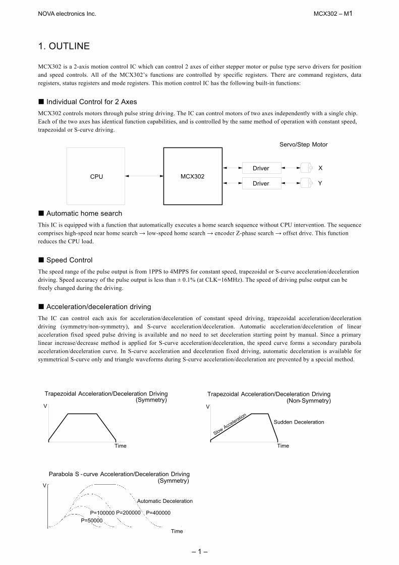
1. OUTLINE MCX302 is a 2-axis motion control IC which can control 2 axes of either stepper motor or pulse type servo drivers for position and speed controls. All of the MCX302’s functions are controlled by specific registers. There are command registers, data registers, status registers and mode registers. This motion control IC has the following built-in functions:
Individual Control for 2 Axes MCX302 controls motors through pulse string driving. The IC can control motors of two axes independently with a single chip. Each of the two axes has identical function capabilities, and is controlled by the same method of operation with constant speed, trapezoidal or S-curve driving.
Automatic home search This IC is equipped with a function that automatically executes a home search sequence without CPU intervention. The sequence comprises high-speed near home search → low-speed home search → encoder Z-phase search → offset drive. This function reduces the CPU load.
Speed Control The speed range of the pulse output is from 1PPS to 4MPPS for constant speed, trapezoidal or S-curve acceleration/deceleration driving. Speed accuracy of the pulse output is less than ± 0.1% (at CLK=16MHz). The speed of driving pulse output can be freely changed during the driving.
Acceleration/deceleration driving The IC can control each axis for acceleration/deceleration of constant speed driving, trapezoidal acceleration/deceleration driving (symmetry/non-symmetry), and S-curve acceleration/deceleration. Automatic acceleration/deceleration of linear acceleration fixed speed pulse driving is available and no need to set deceleration starting point by manual. Since a primary linear increase/decrease method is applied for S-curve acceleration/deceleration, the speed curve forms a secondary parabola acceleration/deceleration curve. In S-curve acceleration and deceleration fixed driving, automatic deceleration is available for symmetrical S-curve only and triangle waveforms during S-curve acceleration/deceleration are prevented by a special method.
DriverMCX302CPU
Driver
Servo/Step Motor
X
Y
Trapezoidal Acceleration/Deceleration Driving Trapezoidal Acceleration/Deceleration Driving
Sudden Deceleration
Time
V
Time
V
Time
V
Automatic Deceleration
Slow Acceleration
P=400000P=200000P=100000P=50000
Parabola S -curve Acceleration/Deceleration Driving(Symmetry)
(Symmetry) (Non-Symmetry)
NOVA electronics Inc. MCX302 – M2
– 2 –
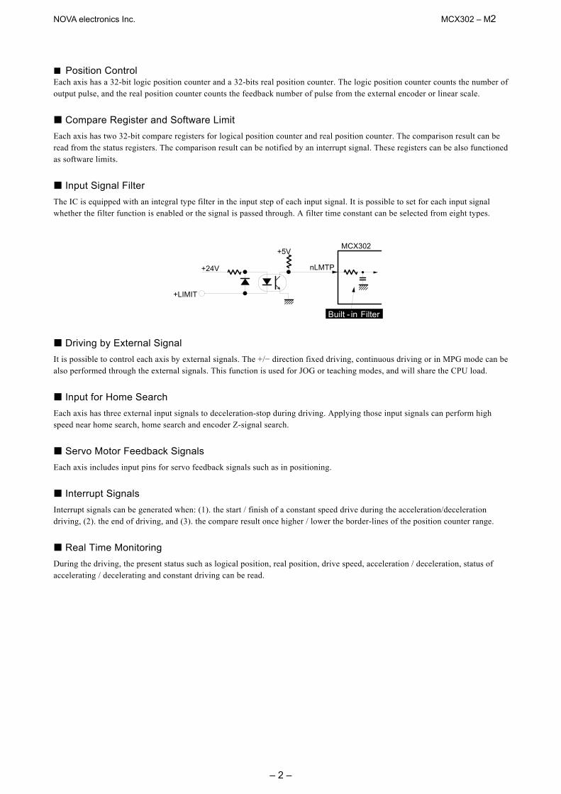
Position Control
Each axis has a 32-bit logic position counter and a 32-bits real position counter. The logic position counter counts the number of output pulse, and the real position counter counts the feedback number of pulse from the external encoder or linear scale.
Compare Register and Software Limit Each axis has two 32-bit compare registers for logical position counter and real position counter. The comparison result can be read from the status registers. The comparison result can be notified by an interrupt signal. These registers can be also functioned as software limits.
Input Signal Filter The IC is equipped with an integral type filter in the input step of each input signal. It is possible to set for each input signal whether the filter function is enabled or the signal is passed through. A filter time constant can be selected from eight types.
Driving by External Signal It is possible to control each axis by external signals. The +/− direction fixed driving, continuous driving or in MPG mode can be also performed through the external signals. This function is used for JOG or teaching modes, and will share the CPU load.
Input for Home Search Each axis has three external input signals to deceleration-stop during driving. Applying those input signals can perform high speed near home search, home search and encoder Z-signal search.
Servo Motor Feedback Signals Each axis includes input pins for servo feedback signals such as in positioning.
Interrupt Signals Interrupt signals can be generated when: (1). the start / finish of a constant speed drive during the acceleration/deceleration driving, (2). the end of driving, and (3). the compare result once higher / lower the border-lines of the position counter range.
Real Time Monitoring During the driving, the present status such as logical position, real position, drive speed, acceleration / deceleration, status of accelerating / decelerating and constant driving can be read.
+LIMIT
+24V
+5VMCX302
nLMTP
Built - in Filter
NOVA electronics Inc. MCX302 – M3
– 3 –
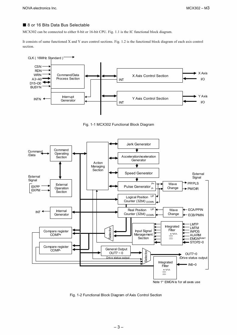
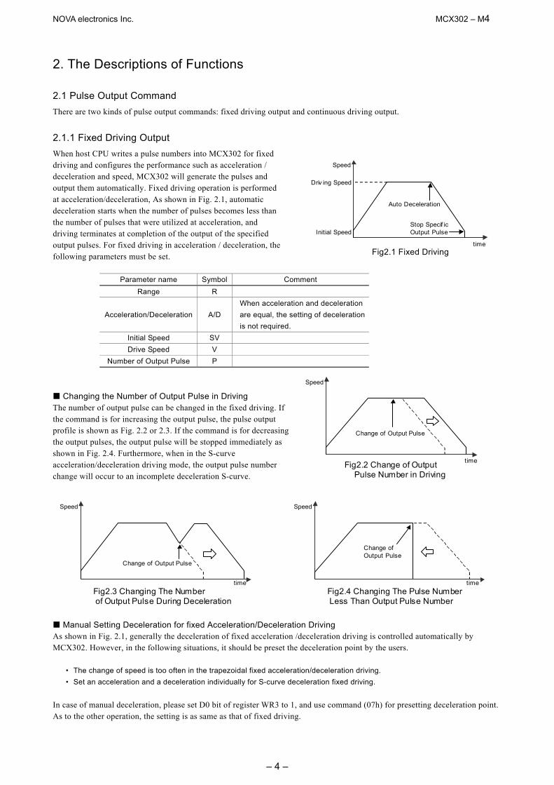
8 or 16 Bits Data Bus Selectable MCX302 can be connected to either 8-bit or 16-bit CPU. Fig. 1.1 is the IC functional block diagram. It consists of same functioned X and Y axes control sections. Fig. 1.2 is the functional block diagram of each axis control section.
Command/Data Process Section
X Axis Control Section INT
Y Axis Control Section INT
Interrupt Generator
CSN RDN
WRN A3~A0
D15~D0 BUSYN
INTN Y Axis
I/O
CLK ( 16MHz Standard )
X Axis
I/O
Fig. 1-1 MCX302 Functional Block Diagram
・
Integrated Filter
Integrated Filter
Command Operating Section
External Operation Section
Internal Generator
Compare register COMP+
Compare register COMP-
Action Managing Section
Jerk Generator
Acceleration/eceleration Generator
Speed Generator
General Output OUT7 ~ 0
Command /Data
External Signal
Wave Change
Wave Change
EXPP EXPM
INT
LMTP LMTM INPOS ALARM EMGN STOP2~0
Note1
OUT7~0 /Drive status output Driv e status output
IN5~0
Note 1* EMGN is for all axes use
External Signal
Logical Position Counter (32bit)
UP
DOWN
Real Position Counter (32bit)
UP
DOWN
Sele
ctor
Sele
ctor
Fig. 1-2 Functional Block Diagram of Axis Control Section
ECA/PPIN ECB/PMIN
PP/PLS PM/DIR Pulse Generator
P+
P-
Input Signal Management
Section
・
NOVA electronics Inc. MCX302 – M4
– 4 –
2. The Descriptions of Functions
2.1 Pulse Output Command There are two kinds of pulse output commands: fixed driving output and continuous driving output.
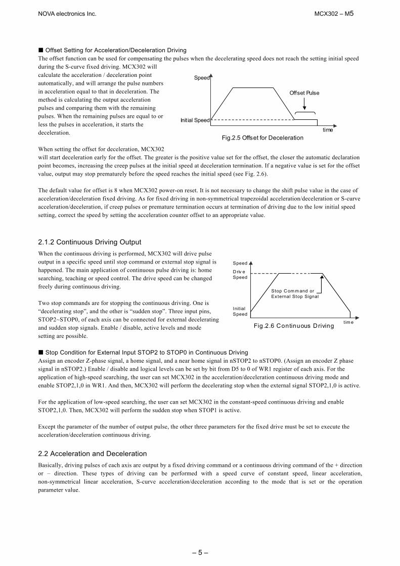
2.1.1 Fixed Driving Output When host CPU writes a pulse numbers into MCX302 for fixed driving and configures the performance such as acceleration / deceleration and speed, MCX302 will generate the pulses and output them automatically. Fixed driving operation is performed at acceleration/deceleration, As shown in Fig. 2.1, automatic deceleration starts when the number of pulses becomes less than the number of pulses that were utilized at acceleration, and driving terminates at completion of the output of the specified output pulses. For fixed driving in acceleration / deceleration, the following parameters must be set.
Parameter name Symbol Comment Range R
Acceleration/Deceleration A/D
When acceleration and deceleration are equal, the setting of deceleration is not required.
Initial Speed SV
Drive Speed V
Number of Output Pulse P
Changing the Number of Output Pulse in Driving The number of output pulse can be changed in the fixed driving. If the command is for increasing the output pulse, the pulse output profile is shown as Fig. 2.2 or 2.3. If the command is for decreasing the output pulses, the output pulse will be stopped immediately as shown in Fig. 2.4. Furthermore, when in the S-curve acceleration/deceleration driving mode, the output pulse number change will occur to an incomplete deceleration S-curve.
Fig2.3 Changing The Number of Output Pulse During Deceleration
Speed
Change of Output Pulse
time
Speed
Change of Output Pulse
time
Fig2.4 Changing The Pulse Number Less Than Output Pulse Number
Manual Setting Deceleration for fixed Acceleration/Deceleration Driving As shown in Fig. 2.1, generally the deceleration of fixed acceleration /deceleration driving is controlled automatically by MCX302. However, in the following situations, it should be preset the deceleration point by the users.
• The change of speed is too often in the trapezoidal fixed acceleration/deceleration driving. • Set an acceleration and a deceleration individually for S-curve deceleration fixed driving.
In case of manual deceleration, please set D0 bit of register WR3 to 1, and use command (07h) for presetting deceleration point. As to the other operation, the setting is as same as that of fixed driving.
Speed
Driv ing Speed
Initial Speed
Auto Deceleration
Stop Specif ic Output Pulse
time
Fig2.1 Fixed Driving
Fig2.2 Change of Output Pulse Number in Driving
Speed
Change of Output Pulse
time
NOVA electronics Inc. MCX302 – M5
– 5 –
Offset Setting for Acceleration/Deceleration Driving
The offset function can be used for compensating the pulses when the decelerating speed does not reach the setting initial speed during the S-curve fixed driving. MCX302 will calculate the acceleration / deceleration point automatically, and will arrange the pulse numbers in acceleration equal to that in deceleration. The method is calculating the output acceleration pulses and comparing them with the remaining pulses. When the remaining pulses are equal to or less the pulses in acceleration, it starts the deceleration. When setting the offset for deceleration, MCX302 will start deceleration early for the offset. The greater is the positive value set for the offset, the closer the automatic declaration point becomes, increasing the creep pulses at the initial speed at deceleration termination. If a negative value is set for the offset value, output may stop prematurely before the speed reaches the initial speed (see Fig. 2.6). The default value for offset is 8 when MCX302 power-on reset. It is not necessary to change the shift pulse value in the case of acceleration/deceleration fixed driving. As for fixed driving in non-symmetrical trapezoidal acceleration/deceleration or S-curve acceleration/deceleration, if creep pulses or premature termination occurs at termination of driving due to the low initial speed setting, correct the speed by setting the acceleration counter offset to an appropriate value.
2.1.2 Continuous Driving Output When the continuous driving is performed, MCX302 will drive pulse output in a specific speed until stop command or external stop signal is happened. The main application of continuous pulse driving is: home searching, teaching or speed control. The drive speed can be changed freely during continuous driving. Two stop commands are for stopping the continuous driving. One is “decelerating stop”, and the other is “sudden stop”. Three input pins, STOP2~STOP0, of each axis can be connected for external decelerating and sudden stop signals. Enable / disable, active levels and mode setting are possible.
Stop Condition for External Input STOP2 to STOP0 in Continuous Driving Assign an encoder Z-phase signal, a home signal, and a near home signal in nSTOP2 to nSTOP0. (Assign an encoder Z phase signal in nSTOP2.) Enable / disable and logical levels can be set by bit from D5 to 0 of WR1 register of each axis. For the application of high-speed searching, the user can set MCX302 in the acceleration/deceleration continuous driving mode and enable STOP2,1,0 in WR1. And then, MCX302 will perform the decelerating stop when the external signal STOP2,1,0 is active. For the application of low-speed searching, the user can set MCX302 in the constant-speed continuous driving and enable STOP2,1,0. Then, MCX302 will perform the sudden stop when STOP1 is active. Except the parameter of the number of output pulse, the other three parameters for the fixed drive must be set to execute the acceleration/deceleration continuous driving.
2.2 Acceleration and Deceleration Basically, driving pulses of each axis are output by a fixed driving command or a continuous driving command of the + direction or – direction. These types of driving can be performed with a speed curve of constant speed, linear acceleration, non-symmetrical linear acceleration, S-curve acceleration/deceleration according to the mode that is set or the operation parameter value.
Speed
D riv e Speed
Init ial Speed
t im e
Stop C om m and or Ex ternal Stop Signal
Fig.2.6 Continuous Driving
Offset Pulse
time
Init ial Speed
Speed
Fig.2.5 Offset for Deceleration
NOVA electronics Inc. MCX302 – M6
– 6 –
2.2.1 Constant Speed Driving When the drive speed set in MCX302 is lower than the initial, the acceleration / deceleration will not be performed, instead, a constant speed driving starts. If the user wants to perform the sudden stop when the home sensor or encoder Z-phase signal is active, it is better not to perform the acceleration / deceleration driving, but the low-speed constant driving from the beginning. For processing constant speed driving, the following parameters will be preset accordingly.
Example for Parameter Setting of Constant Speed The constant speed is set 980 PPS as shown in the right Figure.
Range R = 8,000,000 ; Multiple = 1 Initial Speed SV=980 ; Initial Speed ≥ Drive Speed ; Should be less than initial speed Drive Speed V=980
Please refer each parameter in Chapter 6.
2.2.2 Trapezoidal Driving [Symmetrical] In linear acceleration driving, the drive speed accelerates in a primary linear form with the specified acceleration slope from the initial speed at the start of driving. When the acceleration and the deceleration are the same (symmetrical trapezoid) in fixed driving, the pulses utilized at acceleration are counted. When the remaining number of output pulses becomes less than the number of acceleration pulses, deceleration starts. Deceleration continues in the primary line with the same slope as that of acceleration until the speed reaches the initial speed and driving stops, at completion of the output of all the pulses (automatic deceleration). When the decelerating stop command is performed during the acceleration, or when the pulse numbers of the fixed drive do not reach the designated drive speed, the driving will be decelerating during acceleration, as show in Fig. 2.9. By setting a triangle prevention mode, such triangle form can be transformed to a trapezoid form even if the number of output pulses low. See the section of triangle prevention of fixed driving. To perform symmetrical linear acceleration driving, the following parameters must be set, parameters marked by will be set when needed.
Parameter name Symbol Comment Range R
Initial Speed SV Set a value higher than the drive speed (V).
Drive Speed V
Number of Output Pulse P Not required for continuous driving.
Parameter name Symbol Comment Range R
Acceleration A Acceleration and deceleration.
Deceleration D Deceleration when acceleration and deceleration are set individually.
Initial Speed SV
Drive Speed V
Number of Output Pulse P Not required for continuous driving.
time
Speed
Initial Speed
Driv e Speed
Fig. 2.7 Constant Speed Driving
time (SEC)
Speed (pps)
980
time
Speed
Driv e Speed
Initial Speed
Acceleration (slope)
Output pulse is too low. not sutable for the requirement of driv e speed
Deceleration=Acceleration
Fig. 2.8 Trapezoidal Driving (Symmetrical)
NOVA electronics Inc. MCX302 – M7
– 7 –
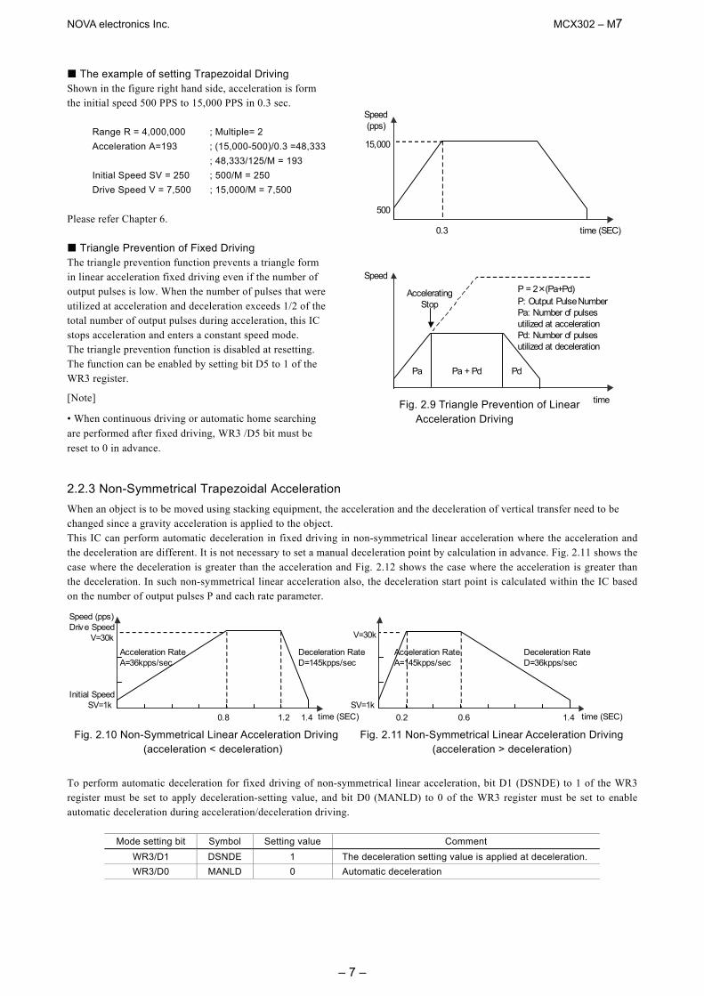
The example of setting Trapezoidal Driving Shown in the figure right hand side, acceleration is form the initial speed 500 PPS to 15,000 PPS in 0.3 sec.
Range R = 4,000,000 ; Multiple= 2 Acceleration A=193 ; (15,000-500)/0.3 =48,333 ; 48,333/125/M = 193 Initial Speed SV = 250 ; 500/M = 250 Drive Speed V = 7,500 ; 15,000/M = 7,500
Please refer Chapter 6.
Triangle Prevention of Fixed Driving The triangle prevention function prevents a triangle form in linear acceleration fixed driving even if the number of output pulses is low. When the number of pulses that were utilized at acceleration and deceleration exceeds 1/2 of the total number of output pulses during acceleration, this IC stops acceleration and enters a constant speed mode. The triangle prevention function is disabled at resetting. The function can be enabled by setting bit D5 to 1 of the WR3 register.
[Note]
• When continuous driving or automatic home searching are performed after fixed driving, WR3 /D5 bit must be reset to 0 in advance.
2.2.3 Non-Symmetrical Trapezoidal Acceleration When an object is to be moved using stacking equipment, the acceleration and the deceleration of vertical transfer need to be changed since a gravity acceleration is applied to the object. This IC can perform automatic deceleration in fixed driving in non-symmetrical linear acceleration where the acceleration and the deceleration are different. It is not necessary to set a manual deceleration point by calculation in advance. Fig. 2.11 shows the case where the deceleration is greater than the acceleration and Fig. 2.12 shows the case where the acceleration is greater than the deceleration. In such non-symmetrical linear acceleration also, the deceleration start point is calculated within the IC based on the number of output pulses P and each rate parameter.
To perform automatic deceleration for fixed driving of non-symmetrical linear acceleration, bit D1 (DSNDE) to 1 of the WR3 register must be set to apply deceleration-setting value, and bit D0 (MANLD) to 0 of the WR3 register must be set to enable automatic deceleration during acceleration/deceleration driving.
Mode setting bit Symbol Setting value Comment WR3/D1 DSNDE 1 The deceleration setting value is applied at deceleration. WR3/D0 MANLD 0 Automatic deceleration
time (SEC)
Speed (pps)
15,000
500
0.3
time
Speed
Pa Pa + Pd Pd
Accelerating Stop
P = 2×(Pa+Pd) P: Output Pulse Number Pa: Number of pulses utilized at acceleration Pd: Number of pulses utilized at deceleration
Fig. 2.9 Triangle Prevention of Linear Acceleration Driving
Fig. 2.10 Non-Symmetrical Linear Acceleration Driving (acceleration < deceleration)
Fig. 2.11 Non-Symmetrical Linear Acceleration Driving (acceleration > deceleration)
Speed (pps) Drive Speed V=30k
Initial Speed SV=1k
V=30k
SV=1k
time (SEC) time (SEC)
Deceleration Rate D=145kpps/sec
Deceleration Rate D=36kpps/sec
Acceleration Rate A=36kpps/sec
Acceleration Rate A=145kpps/sec
0.8 1.2 1.4 0.2 0.6 1.4
NOVA electronics Inc. MCX302 – M8
– 8 –
The following parameters must be set. [Note] • In the case of acceleration > deceleration (Fig. 2.12), the following condition is applied to the ratio of the acceleration and the
deceleration. V D: Deceleration (pps/sec) D > A × A: Acceleration (pps/sec) Where CLK=16MHz 4 × 10⁶ V: Drive Speed (pps)
For instance, if the driving speed V = 100kps, deceleration D must be greater than 1/40 of acceleration A. The value must not be less than 1/40 of the acceleration. • If acceleration > deceleration (Fig. 2.12), the greater the ratio of acceleration A to deceleration D becomes, the greater the
number of creep pulses becomes (about maximum of 10 pulse when A/D=10 times). When creep pulses cause a problem, solve the problem by increasing the initial speed or setting a minus value to the acceleration counter offset.
Parameter name Symbol Comment Range R
Acceleration A
Deceleration D
Initial speed SV
Drive speed V
Number of output pulses P Not required at continuous driving
NOVA electronics Inc. MCX302 – M9
– 9 –
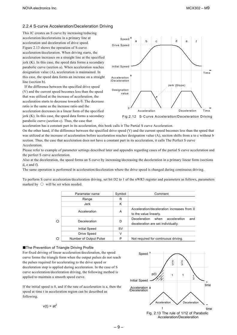
2.2.4 S-curve Acceleration/Deceleration Driving This IC creates an S curve by increasing/reducing acceleration/decelerations in a primary line at acceleration and deceleration of drive speed. Figure 2.13 shows the operation of S-curve acceleration/deceleration. When driving starts, the acceleration increases on a straight line at the specified jerk (K). In this case, the speed data forms a secondary parabolic curve (section a). When acceleration reaches designation value (A), acceleration is maintained. In this case, the speed data forms an increase on a straight line (section b). If the difference between the specified drive speed (V) and the current speed becomes less than the speed that was utilized at the increase of acceleration, the acceleration starts to decrease towards 0. The decrease ratio is the same as the increase ratio and the acceleration decreases in a linear form of the specified jerk (K). In this case, the speed data forms a secondary parabolic curve (section c). Thus, the case that acceleration has a constant part in its acceleration, this book calls it The Partial S curve Acceleration. On the other hand, if the difference between the specified drive speed (V) and the current speed becomes less than the speed that was utilized at the increase of acceleration before acceleration reaches designation value (A), section shifts from a to c without b section. Thus, the case that acceleration does not have a constant part in its acceleration, it calls The Perfect S curve Acceleration. Please refer to example of parameter settings described later and appendix regarding cases of the partial S curve acceleration and the perfect S curve acceleration. Also at the deceleration, the speed forms an S curve by increasing/decreasing the deceleration in a primary linear form (sections d, e and f). The same operation is performed in acceleration/deceleration where the drive speed is changed during continuous driving. To perform S curve acceleration/deceleration driving, set bit D2 to 1 of the nWR3 register and parameters as follows, parameters marked by will be set when needed.
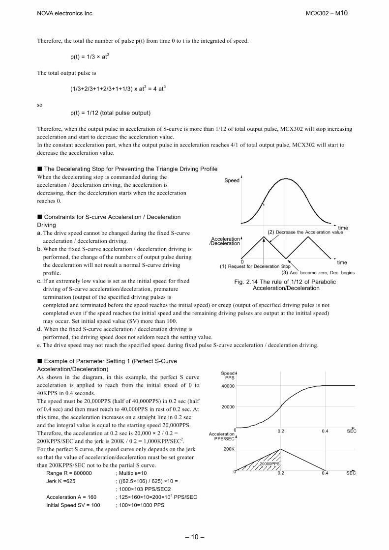
The Prevention of Triangle Driving Profile For fixed driving of linear acceleration/deceleration, the speed curve forms the triangle form when the output pulses do not reach the pulses required for accelerating to the drive speed or deceleration stop is applied during acceleration. In the case of S curve acceleration/deceleration driving, the following method is applied to maintain a smooth speed curve. If the initial speed is 0, and if the rate of acceleration is a, then the speed at time t in acceleration region can be described as following. v(t) = at2
Parameter name Symbol Comment Range R
Jerk K
Acceleration A
Acceleration/deceleration increases from 0 to the value linearly.
Deceleration D Deceleration when acceleration and deceleration are set individually.
Initial Speed SV
Drive Speed V
Number of Output Pulse P Not required for continuous driving.
Acceleration
T im e
Speed
T im e
In itia l Speed
Acceleration D eceleration
D rive Speed
D esignation
Jerk (S lope)
0
F ig .2.12 S- C urve Acceleration/D eceleration D riv ing
a b c d e f
/Deceleration
value
p(t)
32
Fig. 2.13 The rule of 1/12 of ParabolicAcceleration/Deceleration
32
11
t time
Speed
Initial Speed
Acceleration/Deceleration
Acceleration Deceleration
31
time
31
NOVA electronics Inc. MCX302 – M10
– 10 –
Therefore, the total the number of pulse p(t) from time 0 to t is the integrated of speed. p(t) = 1/3 × at3 The total output pulse is (1/3+2/3+1+2/3+1+1/3) x at3 = 4 at3
so p(t) = 1/12 (total pulse output) Therefore, when the output pulse in acceleration of S-curve is more than 1/12 of total output pulse, MCX302 will stop increasing acceleration and start to decrease the acceleration value. In the constant acceleration part, when the output pulse in acceleration reaches 4/1 of total output pulse, MCX302 will start to decrease the acceleration value.
The Decelerating Stop for Preventing the Triangle Driving Profile When the decelerating stop is commanded during the acceleration / deceleration driving, the acceleration is decreasing, then the deceleration starts when the acceleration reaches 0.
Constraints for S-curve Acceleration / Deceleration Driving a. The drive speed cannot be changed during the fixed S-curve
acceleration / deceleration driving. b. When the fixed S-curve acceleration / deceleration driving is
performed, the change of the numbers of output pulse during the deceleration will not result a normal S-curve driving profile.
c. If an extremely low value is set as the initial speed for fixed driving of S-curve acceleration/deceleration, premature termination (output of the specified driving pulses is completed and terminated before the speed reaches the initial speed) or creep (output of specified driving pules is not
completed even if the speed reaches the initial speed and the remaining driving pulses are output at the initital speed) may occur. Set initial speed value (SV) more than 100.
d. When the fixed S-curve acceleration / deceleration driving is performed, the driving speed does not seldom reach the setting value.
e. The drive speed may not reach the specified speed during fixed pulse S-curve acceleration / deceleration driving.
Example of Parameter Setting 1 (Perfect S-Curve Acceleration/Deceleration) As shown in the diagram, in this example, the perfect S curve acceleration is applied to reach from the initial speed of 0 to 40KPPS in 0.4 seconds. The speed must be 20,000PPS (half of 40,000PPS) in 0.2 sec (half of 0.4 sec) and then must reach to 40,000PPS in rest of 0.2 sec. At this time, the acceleration increases on a straight line in 0.2 sec and the integral value is equal to the starting speed 20,000PPS. Therefore, the acceleration at 0.2 sec is 20,000 × 2 / 0.2 = 200KPPS/SEC and the jerk is 200K / 0.2 = 1,000KPP/SEC2. For the perfect S curve, the speed curve only depends on the jerk so that the value of acceleration/deceleration must be set greater than 200KPPS/SEC not to be the partial S curve.
Range R = 800000 ; Multiple=10 Jerk K =625 ; ((62.5×10⁶) / 625) ×10 = ; 1000×103 PPS/SEC2 Acceleration A = 160 ; 125×160×10=200×103 PPS/SEC Initial Speed SV = 100 ; 100×10=1000 PPS
0(1) Request for Deceleration Stop
(2) Decrease the Acceleration value
(3) Acc. become zero, Dec. begins
Speed
Acceleration/Deceleration
time
time
Fig. 2.14 The rule of 1/12 of ParabolicAcceleration/Deceleration
20000PPS
0.2 0.4 SEC
AccelerationPPS/SEC
200K
0
0.2 0.4 SEC
20000
40000
SpeedPPS
0
NOVA electronics Inc. MCX302 – M11
– 11 –
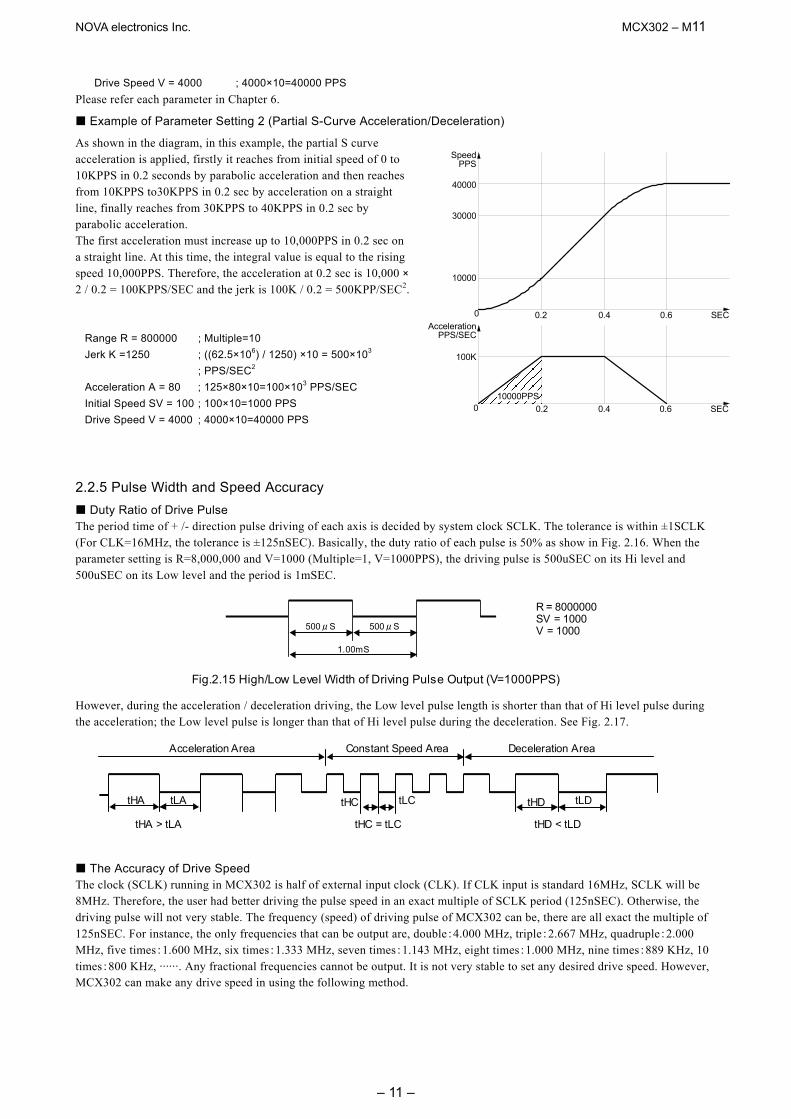
Drive Speed V = 4000 ; 4000×10=40000 PPS Please refer each parameter in Chapter 6.
Example of Parameter Setting 2 (Partial S-Curve Acceleration/Deceleration)
As shown in the diagram, in this example, the partial S curve acceleration is applied, firstly it reaches from initial speed of 0 to 10KPPS in 0.2 seconds by parabolic acceleration and then reaches from 10KPPS to30KPPS in 0.2 sec by acceleration on a straight line, finally reaches from 30KPPS to 40KPPS in 0.2 sec by parabolic acceleration. The first acceleration must increase up to 10,000PPS in 0.2 sec on a straight line. At this time, the integral value is equal to the rising speed 10,000PPS. Therefore, the acceleration at 0.2 sec is 10,000 × 2 / 0.2 = 100KPPS/SEC and the jerk is 100K / 0.2 = 500KPP/SEC2.
Range R = 800000 ; Multiple=10 Jerk K =1250 ; ((62.5×10⁶) / 1250) ×10 = 500×103 ; PPS/SEC2 Acceleration A = 80 ; 125×80×10=100×103 PPS/SEC Initial Speed SV = 100 ; 100×10=1000 PPS Drive Speed V = 4000 ; 4000×10=40000 PPS
2.2.5 Pulse Width and Speed Accuracy
Duty Ratio of Drive Pulse The period time of + /- direction pulse driving of each axis is decided by system clock SCLK. The tolerance is within ±1SCLK (For CLK=16MHz, the tolerance is ±125nSEC). Basically, the duty ratio of each pulse is 50% as show in Fig. 2.16. When the parameter setting is R=8,000,000 and V=1000 (Multiple=1, V=1000PPS), the driving pulse is 500uSEC on its Hi level and 500uSEC on its Low level and the period is 1mSEC.
500μS 500μS
1.00mS
R = 8000000 SV = 1000 V = 1000
Fig.2.15 High/Low Level Width of Driving Pulse Output (V=1000PPS)
However, during the acceleration / deceleration driving, the Low level pulse length is shorter than that of Hi level pulse during the acceleration; the Low level pulse is longer than that of Hi level pulse during the deceleration. See Fig. 2.17.
tLD
tLA
tHA
tHA > tLA
tHC
tLC
tHC = tLC
tHD
tHD < tLD
Acceleration Area
Constant Speed Area
Deceleration Area
The Accuracy of Drive Speed The clock (SCLK) running in MCX302 is half of external input clock (CLK). If CLK input is standard 16MHz, SCLK will be 8MHz. Therefore, the user had better driving the pulse speed in an exact multiple of SCLK period (125nSEC). Otherwise, the driving pulse will not very stable. The frequency (speed) of driving pulse of MCX302 can be, there are all exact the multiple of 125nSEC. For instance, the only frequencies that can be output are, double:4.000 MHz, triple:2.667 MHz, quadruple:2.000 MHz, five times:1.600 MHz, six times:1.333 MHz, seven times:1.143 MHz, eight times:1.000 MHz, nine times:889 KHz, 10 times:800 KHz, ······. Any fractional frequencies cannot be output. It is not very stable to set any desired drive speed. However, MCX302 can make any drive speed in using the following method.
0.60.40.20
10000
30000
40000
PPSSpeed
SECAcceleration
PPS/SEC
0 0.2 0.4 0.6 SEC
100K
10000PPS
NOVA electronics Inc. MCX302 – M12
– 12 –
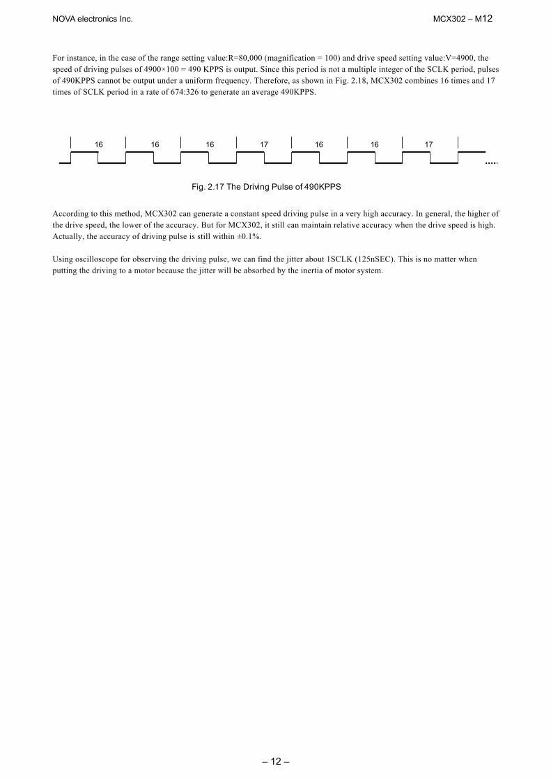
For instance, in the case of the range setting value:R=80,000 (magnification = 100) and drive speed setting value:V=4900, the speed of driving pulses of 4900×100 = 490 KPPS is output. Since this period is not a multiple integer of the SCLK period, pulses of 490KPPS cannot be output under a uniform frequency. Therefore, as shown in Fig. 2.18, MCX302 combines 16 times and 17 times of SCLK period in a rate of 674:326 to generate an average 490KPPS.
According to this method, MCX302 can generate a constant speed driving pulse in a very high accuracy. In general, the higher of the drive speed, the lower of the accuracy. But for MCX302, it still can maintain relative accuracy when the drive speed is high. Actually, the accuracy of driving pulse is still within ±0.1%. Using oscilloscope for observing the driving pulse, we can find the jitter about 1SCLK (125nSEC). This is no matter when putting the driving to a motor because the jitter will be absorbed by the inertia of motor system.
16 16 16 17 16 17 16
Fig. 2.17 The Driving Pulse of 490KPPS
NOVA electronics Inc. MCX302 – M13
– 13 –
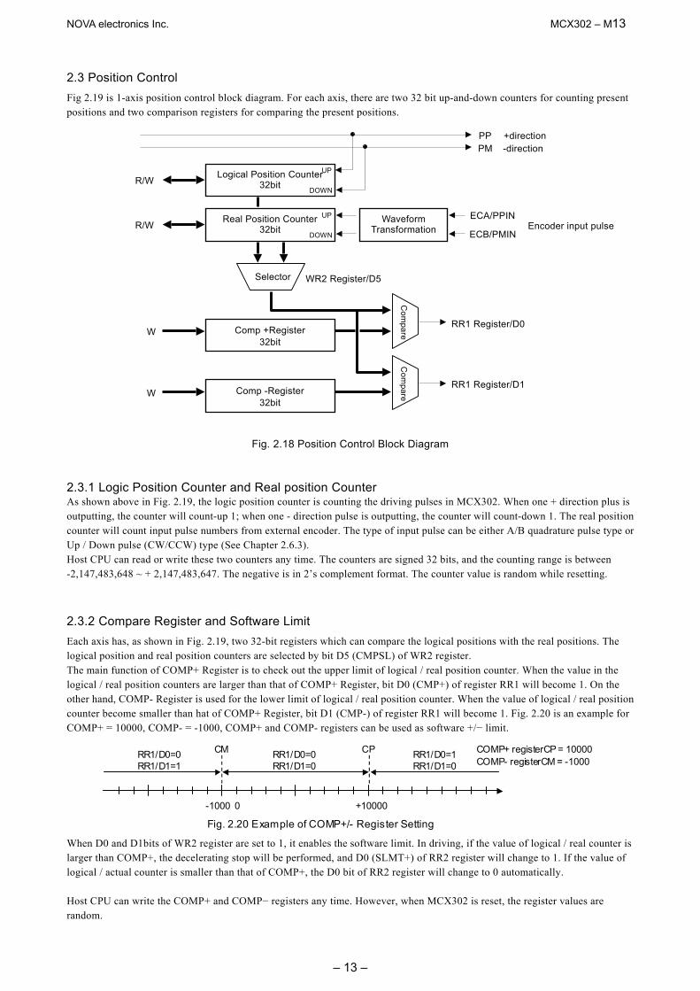
2.3 Position Control Fig 2.19 is 1-axis position control block diagram. For each axis, there are two 32 bit up-and-down counters for counting present positions and two comparison registers for comparing the present positions.
Fig. 2.18 Position Control Block Diagram 2.3.1 Logic Position Counter and Real position Counter As shown above in Fig. 2.19, the logic position counter is counting the driving pulses in MCX302. When one + direction plus is outputting, the counter will count-up 1; when one - direction pulse is outputting, the counter will count-down 1. The real position counter will count input pulse numbers from external encoder. The type of input pulse can be either A/B quadrature pulse type or Up / Down pulse (CW/CCW) type (See Chapter 2.6.3). Host CPU can read or write these two counters any time. The counters are signed 32 bits, and the counting range is between -2,147,483,648 ~ + 2,147,483,647. The negative is in 2’s complement format. The counter value is random while resetting.
2.3.2 Compare Register and Software Limit Each axis has, as shown in Fig. 2.19, two 32-bit registers which can compare the logical positions with the real positions. The logical position and real position counters are selected by bit D5 (CMPSL) of WR2 register. The main function of COMP+ Register is to check out the upper limit of logical / real position counter. When the value in the logical / real position counters are larger than that of COMP+ Register, bit D0 (CMP+) of register RR1 will become 1. On the other hand, COMP- Register is used for the lower limit of logical / real position counter. When the value of logical / real position counter become smaller than hat of COMP+ Register, bit D1 (CMP-) of register RR1 will become 1. Fig. 2.20 is an example for COMP+ = 10000, COMP- = -1000, COMP+ and COMP- registers can be used as software +/− limit.
-1000 +10000 0
CM CP RR1/D0=0 RR1/D1=1
RR1/D0=0 RR1/D1=0
RR1/D0=1 RR1/D1=0
COMP+ registerCP = 10000
COMP- registerCM = -1000
Fig. 2.20 Example of COMP+/- Register Setting When D0 and D1bits of WR2 register are set to 1, it enables the software limit. In driving, if the value of logical / real counter is larger than COMP+, the decelerating stop will be performed, and D0 (SLMT+) of RR2 register will change to 1. If the value of logical / actual counter is smaller than that of COMP+, the D0 bit of RR2 register will change to 0 automatically. Host CPU can write the COMP+ and COMP− registers any time. However, when MCX302 is reset, the register values are random.
PP +direction
Waveform Transformation
Com
pare
Com
pare
Logical Position Counter32bit R/W
Real Position Counter32bit R/W
Comp +Register 32bit
W
Comp -Register 32bit
W
WR2 Register/D5
ECA/PPIN
ECB/PMIN
PM -direction
UP
DOWN
RR1 Register/D0
RR1 Register/D1
UP
DOWNEncoder input pulse
Selector
NOVA electronics Inc. MCX302 – M14
– 14 –
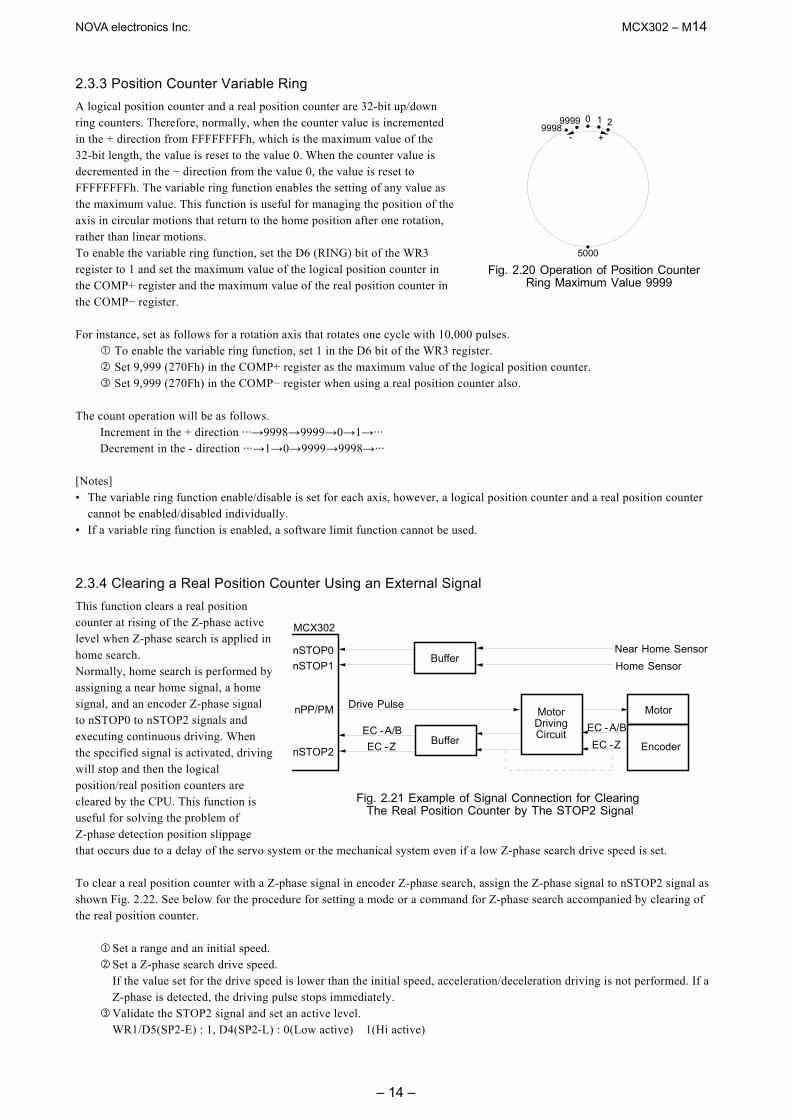
2.3.3 Position Counter Variable Ring A logical position counter and a real position counter are 32-bit up/down ring counters. Therefore, normally, when the counter value is incremented in the + direction from FFFFFFFFh, which is the maximum value of the 32-bit length, the value is reset to the value 0. When the counter value is decremented in the − direction from the value 0, the value is reset to FFFFFFFFh. The variable ring function enables the setting of any value as the maximum value. This function is useful for managing the position of the axis in circular motions that return to the home position after one rotation, rather than linear motions. To enable the variable ring function, set the D6 (RING) bit of the WR3 register to 1 and set the maximum value of the logical position counter in the COMP+ register and the maximum value of the real position counter in the COMP− register. For instance, set as follows for a rotation axis that rotates one cycle with 10,000 pulses.
To enable the variable ring function, set 1 in the D6 bit of the WR3 register. Set 9,999 (270Fh) in the COMP+ register as the maximum value of the logical position counter. Set 9,999 (270Fh) in the COMP− register when using a real position counter also.
The count operation will be as follows.
Increment in the + direction ···→9998→9999→0→1→··· Decrement in the - direction ···→1→0→9999→9998→···
[Notes] • The variable ring function enable/disable is set for each axis, however, a logical position counter and a real position counter
cannot be enabled/disabled individually. • If a variable ring function is enabled, a software limit function cannot be used.
2.3.4 Clearing a Real Position Counter Using an External Signal This function clears a real position counter at rising of the Z-phase active level when Z-phase search is applied in home search. Normally, home search is performed by assigning a near home signal, a home signal, and an encoder Z-phase signal to nSTOP0 to nSTOP2 signals and executing continuous driving. When the specified signal is activated, driving will stop and then the logical position/real position counters are cleared by the CPU. This function is useful for solving the problem of Z-phase detection position slippage that occurs due to a delay of the servo system or the mechanical system even if a low Z-phase search drive speed is set. To clear a real position counter with a Z-phase signal in encoder Z-phase search, assign the Z-phase signal to nSTOP2 signal as shown Fig. 2.22. See below for the procedure for setting a mode or a command for Z-phase search accompanied by clearing of the real position counter.
Set a range and an initial speed. Set a Z-phase search drive speed. If the value set for the drive speed is lower than the initial speed, acceleration/deceleration driving is not performed. If a Z-phase is detected, the driving pulse stops immediately. Validate the STOP2 signal and set an active level. WR1/D5(SP2-E) : 1, D4(SP2-L) : 0(Low active) 1(Hi active)
09999
+-
5000
19998 2
Fig. 2.20 Operation of Position CounterRing Maximum Value 9999
Encoder
MotorEC -A/BEC -Z
MCX302
nSTOP2BufferEC -Z
MotorDrivingCircuit
Fig. 2.21 Example of Signal Connection for ClearingThe Real Position Counter by The STOP2 Signal
nSTOP1nSTOP0
BufferHome SensorNear Home Sensor
EC -A/B
nPP/PM Drive Pulse
NOVA electronics Inc. MCX302 – M15
– 15 –
Enable the clearing of the real position counter using the STOP2 signal. Set WR1/D6 to 1 Issue the + direction or - direction continuous driving command.
As a result of the operations described above, driving starts in the specified direction as shown in Fig. 2.23. When the Z-phase signal reaches an active level, the driving pulses stop and the real position counter is cleared at the rising of the Z-phase signal active level.
[Notes] • Only the nSTOP2 signal can clear the real position counter. The nSTOP1 and nSTOP0 signals cannot clear the counter. • When the input signal filter is invalid, an active level width of more than 4CLK cycles is necessary. When the input signal
filter is valid, a time more than double the input signal delay time is necessary. • It is recommended to perform Z-phase search from the one direction to enhance the position detection precision. • When the nSTOP2 signal is already set to an active level at setting WR1/D6, 5, 4, the real position counter is cleared even if
WR1/D6, 5, 4 is set.
Active Hi
Driving PulseEC -AEC -B
STOP2(EC -Z)Real Position Counter N N+1 N+2 N+3 N+4 N+5 N+6 N+7 0
Fig. 2.22 Example of Operation of Clearing The Real Position Counter Using The STOP2 Sign
Z-Phase Search Stop
NOVA electronics Inc. MCX302 – M16
– 16 –
2.4 Automatic Home Search This IC has a function that automatically executes a home search sequence such as high-speed near home search → low-speed home search → encoder Z-phase search → offset driving without CPU intervention. The automatic home search function sequentially executes the steps from step 1 to step 4 that are listed below. Set execution/non-execution and a search direction mode for each step. In steps 1 and 4, search operation is performed at the high-speed that is set in the drive speed. In steps 2 and 3, search operation is performed at the low-speed that is set in the home search speed.
Step number Operation Search speed Detection signal Step 1 High-speed near home search Drive speed (V) nSTOP0 *1
Step 2 Low-speed home search Home search speed (HV) nSTOP1 *1
Step 3 Low-speed Z-phase search Home search speed (HV) nSTOP2 Step 4 High-speed offset drive Drive speed (V) -
*1: By inputting a home signal in both nSTOP0 and nSTOP1, high-speed search is enabled by using only one home signal. (See “Example of home search using a home signal only” in Section 2.4.7).
2.4.1 Operation of Each Step In each step, it is possible to specify, in mode setting, execution/non-execution and the +/− search direction. If non-execution is specified, the function proceeds with the next step without executing the step.
Step 1: High-speed near home search Drive pulses are output in the specified direction at the speed that is set in the drive speed (V) until the near home signal (nSTOP0) becomes active. To perform high-speed search operation, set a higher value for the drive speed (V) than the initial speed (SV). Acceleration/deceleration driving is performed and when the near home signal (nSTOP0) becomes active, the operation stops by decelerating. Irregular operation (1) The near home signal (nSTOP0) is already active before Step 1 starts. → Proceeds with Step 2. (2) The limit signal in the detection direction is already active before Step 1 starts. → Proceeds with Step 2. (3) The limit signal in the detection direction is activated during execution. → Stops driving and proceeds with Step 2.
Active Section
Active Section
Deceleration Stop at Detection of Near Home
Instant Stop at Detection of Home
Instant Stop at Detection of Z-phase
Encoder Z-phase (STOP2)
N ・HOME (STOP0)
HOME (STOP1)
Step 1 High-speed Near Home Search
Step 2 Low-speed Home Search
Step 3 Low-speed Z-phase Search
Step 4 High-speed Offset Drive
Fig. 2.23 Prototype of Automatic Home Search Using This IC
Active Section
Active Section
STOP0
Over Run Limit in the Search Direction
Specif ied Search Direction
Irregular (1) Irregular (2)
Irregular (3)
NOVA electronics Inc. MCX302 – M17
– 17 –
Step 2: Low-speed home search Drive pulses are output in the specified direction at the speed that is set as the home detection speed (HV) until the home signal (nSTOP1) becomes active. To perform low-search operation, set a lower value for the home search speed (HV) than the initial speed (SV). A constant speed driving mode is applied and the operation stops instantly when the home signal (nSTOP1) becomes active. Irregular operation (1) The home signal (nSTOP1) is already active before Step 2 starts.
→The motor drives the axis in the direction opposite to the specified search direction at the home search speed (HV) until the home signal (nSTOP1) becomes inactive. When the home signal (nSTOP1) becomes inactive, the function executes Step 2 from the beginning.
(2) The limit signal in the search direction is active before Step 2 starts. →The motor drives the axis in the direction opposite to the specified search direction at the home search speed (HV) until the home signal (nSTOP1) becomes active. When the home signal (nSTOP1) becomes active, the motor drives in the direction opposite to the specified search direction at the home search speed (HV) until the home signal (nSTOP1) becomes inactive. When the home signal (nSTOP1) becomes inactive, the function executes Step 2 from the beginning.
(3) The limit signal in the search direction becomes active during execution. →Driving stops and the same operation as for (2)→ is performed.
Step 3: Low-speed Z-phase search
Drive pulses are output in the specified direction at the speed that is set as the home search speed (HV) until the encoder Z-phase signal (nSTOP2) becomes active. To perform low-speed search operation, set a lower value for the home search speed (HV) than the initial speed (SV). A fixed speed driving mode is applied and driving stops instantly when the encoder Z-phase signal (nSTOP2) becomes active. As the search condition for stopping driving, the AND condition of the encoder Z-phase signal (nSTOP2) and the home signal (nSTOP1) can be applied. A deviation counter clear signal can be output for a servomotor when the encoder Z-phase signal (nSTOP2) rises to active. See Section 2.4.2. The real position counter (EP) can be cleared when an encoder Z-phase signal (nSTOP2) rises to active. See Section 2.3.4. [Notes] (1) If the encoder Z-phase signal (nSTOP2) is already active at the start of Step 3, an error occurs and 1 is set in bit D7 of the nRR2 register. Automatic home search ends. Adjust the mechanical system so that Step 3 always starts from anSTOPactive state with a stable encoder Z-phase signal (nSTOP2). (2) If the limit signal in the search direction is already active before the start of Step 3, an error occurs and 1 is set in the search direction limit error bit (D2 or D3) of the nRR2 register. Automatic home search ends. (3) If the limit signal in the search direction becomes active during execution, search operation is interrupted and 1 is set in the search direction limit error bit (D2 or D3) of the nRR2 register. Automatic home search ends.
Step 4: High-speed offset drive The function outputs as many driving pulses as the output pulse numbers (P) that is set, in the specified direction at the speed that is set in the drive speed (V). Use this step to move the axis from the mechanical home position to the operation home position. Through mode setting, the logical position counter and real position counter can be cleared after moving. If the drive direction limit signal becomes active before the start or during execution of Step 4, the operation stops due to an error and 1 is set in the search direction limit error bit (D2 or D3) of the nRR2 register.
Active Section
Active Section
Exit
Exit
Normal Operation
STOP1
Over Run Limit in thSearch Direction
Specif ied Search Direction
Irregular (1)
Irregular (3)
To Normal Operation
Irregular (2)
STOP1 Search in the Opposite Direction
Active Section
Active Section
STOP2 Over Run Limit in the
Search Direction
Normal Operation
Specif ied Search Direction
Error (1) Error (2)
Error (3)
NOVA electronics Inc. MCX302 – M18
– 18 –
2.4.2 Deviation Counter Clearing Signal Output This function outputs a deviation counter clearing signal, by setting a mode, at the activation of the encoder Z-phase signal (nSTOP2) in Step 3 operation. For deviation counter clearing output, the pin is shared with nOUT0, ACASND and DCC output signals. For the clearing pulse, the logical level and the pulse width within the range from 10μsec to 20msec can be specified.
Encoder Z-phase (STOP2)
Step 3 low-speed Z-phase Search
Deviation Counter Clear (OUT0) 10μ ~20msec
Stop
Active
Deviation counter clearing output becomes active at termination of Z-phase search operation in Step 3, and Step 4 starts after completion of clearing pulse output. Deviation counter clearing pulses can also be output by a single command (deviation counter clear command (63h)) instead of an automatic home search sequence. However, the mode following the deviation counter clearing output must be set in advance using an automatic home search mode setting command (60h).
D11(DCC-E) Disable/enable: 1 enable D12(DCC-L) Logical level: 0 or 1 D15 ~ D13(DCCW2 ~ 0) Pulse width: 0~7
2.4.3 Setting a Search Speed and a Mode To perform automatic home search, the following speed parameters and mode must be set.
Setting speed parameters
Speed parameter Command code Description
Drive speed (V) 05
High-speed search speed that is applied in Steps 1 and 4. The range (R), acceleration (A), and initial speed (SV) must also be set to appropriate values to perform acceleration/deceleration driving. See Section 2.2.2.
Home search speed (HV) 61 Low-speed search speed that is applied in Steps 2 and 3. Set a value lower than the initial speed (SV) to stop operation instantly when the search signal becomes active. See Section 2.2.1.
Setting an automatic home search mode
Use an automatic home search mode setting command (60h) to set an automatic search mode. As shown below, set each bit of the WR6 register and then write the command code with axis assignment to WR0 register.
D0
ST1-E DCCW2 DCCW1 DCCW0 DCC-L DCC-E LIMIT SAND PCLR ST4-D ST4-E ST3-D ST3-E ST2-D ST2-E ST1-D
D15 D14 D13 D12 D11 D10 D9 D8 D7 D6 D5 D4 D3 D2 D1
H L
Deviation Counter Clear Output Step 4 Step 3 Step 2 Step 1
WR6
D6,4,2,0 STm-E Specify whether operation of each step is executed. 0: Non-execution 1: Execution Use the WR1 register for logical setting of the input signal that is detected in each step. See
Section 4.4 D7,5,3,1 STm-D Specify search/operation direction of each step. 0: + direction, 1: − direction D8 PCLR When this bit is set to 1, the logical position counter and the real position counter are cleared
at termination of Step 4.
NOVA electronics Inc. MCX302 – M19
– 19 –
D9 SAND When this bit is set to 1, operation of Step 3 stops when the home signal (nSTOP1) and the encoder Z-phase signal (nSTOP2) become active.
D10 LIMIT Set this bit to 1 when setting automatic home search using an overrun limit signal(nLMTP or nLMTM).
D11 DCC-E This bit enables/disables deviation counter clearing output. 0:Enable, 1:Disable For deviation counter clearing output, the pin is shared with nOUT0, ACASND and DCC output
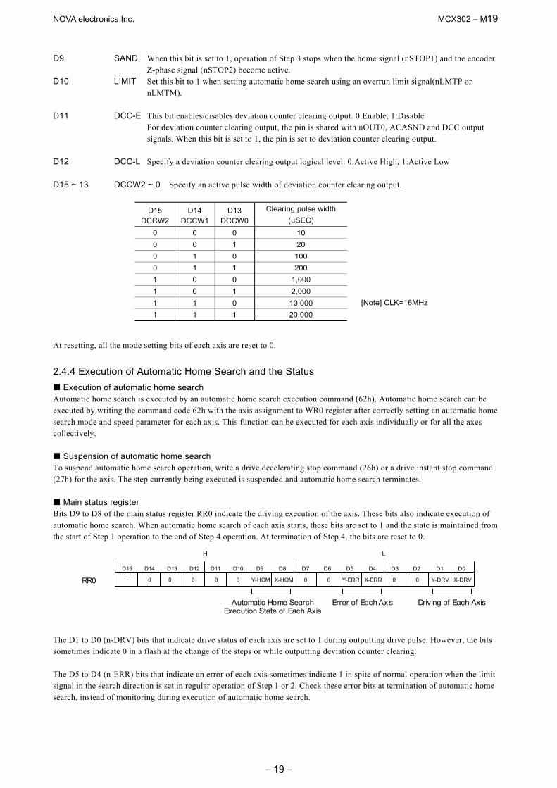
signals. When this bit is set to 1, the pin is set to deviation counter clearing output. D12 DCC-L Specify a deviation counter clearing output logical level. 0:Active High, 1:Active Low D15 ~ 13 DCCW2 ~ 0 Specify an active pulse width of deviation counter clearing output. At resetting, all the mode setting bits of each axis are reset to 0.
2.4.4 Execution of Automatic Home Search and the Status Execution of automatic home search
Automatic home search is executed by an automatic home search execution command (62h). Automatic home search can be executed by writing the command code 62h with the axis assignment to WR0 register after correctly setting an automatic home search mode and speed parameter for each axis. This function can be executed for each axis individually or for all the axes collectively.
Suspension of automatic home search To suspend automatic home search operation, write a drive decelerating stop command (26h) or a drive instant stop command (27h) for the axis. The step currently being executed is suspended and automatic home search terminates.
Main status register Bits D9 to D8 of the main status register RR0 indicate the driving execution of the axis. These bits also indicate execution of automatic home search. When automatic home search of each axis starts, these bits are set to 1 and the state is maintained from the start of Step 1 operation to the end of Step 4 operation. At termination of Step 4, the bits are reset to 0.
- 0 Y-HOM X-HOM
D15 D14 D13 D12 D11 D10 D9 D8 D7 D6 D5 D4 D3 D2 D1 D0
H L
Automatic Home Search Execution State of Each Axis
Error of Each Axis Driving of Each Axis
RR0 0 0 0 0 0 0 Y-ERR X-ERR 0 0 Y-DRV X-DRV
The D1 to D0 (n-DRV) bits that indicate drive status of each axis are set to 1 during outputting drive pulse. However, the bits sometimes indicate 0 in a flash at the change of the steps or while outputting deviation counter clearing. The D5 to D4 (n-ERR) bits that indicate an error of each axis sometimes indicate 1 in spite of normal operation when the limit signal in the search direction is set in regular operation of Step 1 or 2. Check these error bits at termination of automatic home search, instead of monitoring during execution of automatic home search.
D15 DCCW2
D14 DCCW1
D13 DCCW0
Clearing pulse width (μSEC)
0 0 0 10 0 0 1 20 0 1 0 100 0 1 1 200 1 0 0 1,000 1 0 1 2,000 1 1 0 10,000 1 1 1 20,000
[Note] CLK=16MHz
NOVA electronics Inc. MCX302 – M20
– 20 –
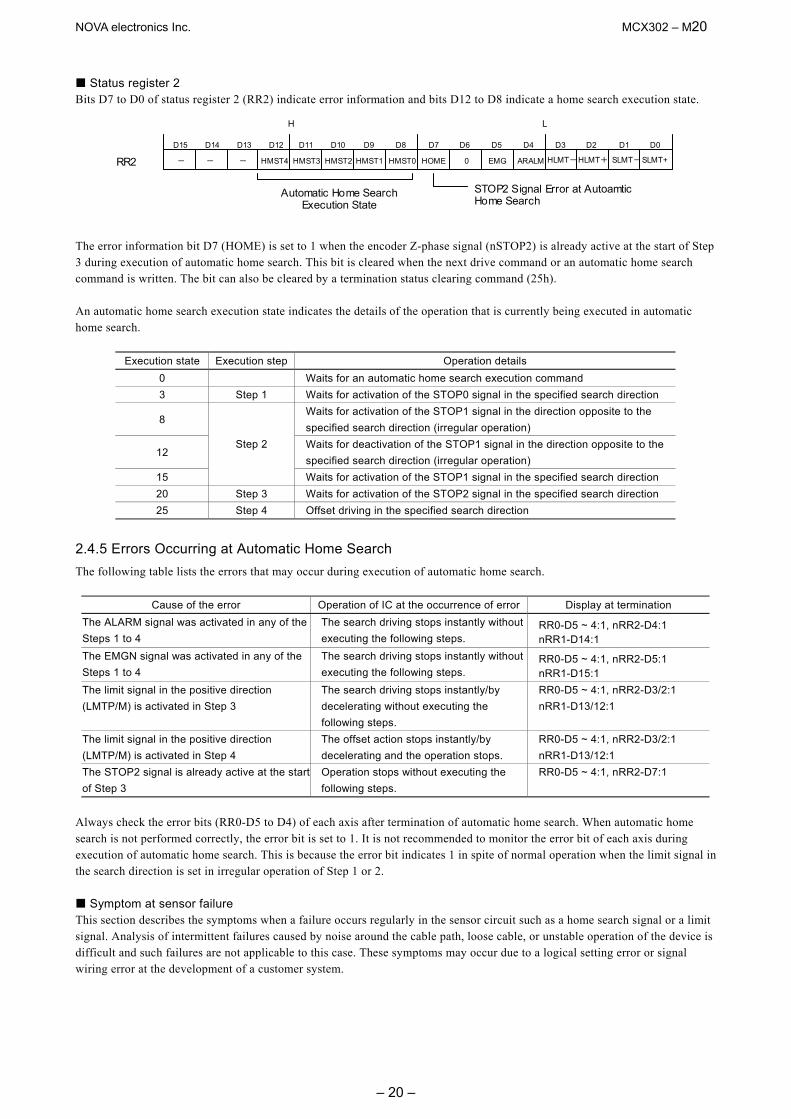
Status register 2 Bits D7 to D0 of status register 2 (RR2) indicate error information and bits D12 to D8 indicate a home search execution state.
-
D15 D14 D13 D12 D11 D10 D9 D8 D7 D6 D5 D4 D3 D2 D1 D0
H L
Automatic Home Search Execution State
STOP2 Signal Error at Autoamtic Home Search
RR2 HMST4 HOME 0 EMG ARALM HLMT- SLMT- SLMT+ - - HMST3 HMST2 HMST1 HMST0 HLMT+
The error information bit D7 (HOME) is set to 1 when the encoder Z-phase signal (nSTOP2) is already active at the start of Step 3 during execution of automatic home search. This bit is cleared when the next drive command or an automatic home search command is written. The bit can also be cleared by a termination status clearing command (25h). An automatic home search execution state indicates the details of the operation that is currently being executed in automatic home search.
Execution state Execution step Operation details 0 Waits for an automatic home search execution command 3 Step 1 Waits for activation of the STOP0 signal in the specified search direction
8 Waits for activation of the STOP1 signal in the direction opposite to the specified search direction (irregular operation)
12 Waits for deactivation of the STOP1 signal in the direction opposite to the specified search direction (irregular operation)
15
Step 2
Waits for activation of the STOP1 signal in the specified search direction 20 Step 3 Waits for activation of the STOP2 signal in the specified search direction 25 Step 4 Offset driving in the specified search direction
2.4.5 Errors Occurring at Automatic Home Search The following table lists the errors that may occur during execution of automatic home search.
Cause of the error Operation of IC at the occurrence of error Display at termination The ALARM signal was activated in any of the Steps 1 to 4
The search driving stops instantly without executing the following steps.
RR0-D5 ~ 4:1, nRR2-D4:1 nRR1-D14:1
The EMGN signal was activated in any of the Steps 1 to 4
The search driving stops instantly without executing the following steps.
RR0-D5 ~ 4:1, nRR2-D5:1 nRR1-D15:1
The limit signal in the positive direction (LMTP/M) is activated in Step 3
The search driving stops instantly/by decelerating without executing the following steps.
RR0-D5 ~ 4:1, nRR2-D3/2:1 nRR1-D13/12:1
The limit signal in the positive direction (LMTP/M) is activated in Step 4
The offset action stops instantly/by decelerating and the operation stops.
RR0-D5 ~ 4:1, nRR2-D3/2:1 nRR1-D13/12:1
The STOP2 signal is already active at the start of Step 3
Operation stops without executing the following steps.
RR0-D5 ~ 4:1, nRR2-D7:1
Always check the error bits (RR0-D5 to D4) of each axis after termination of automatic home search. When automatic home search is not performed correctly, the error bit is set to 1. It is not recommended to monitor the error bit of each axis during execution of automatic home search. This is because the error bit indicates 1 in spite of normal operation when the limit signal in the search direction is set in irregular operation of Step 1 or 2.
Symptom at sensor failure This section describes the symptoms when a failure occurs regularly in the sensor circuit such as a home search signal or a limit signal. Analysis of intermittent failures caused by noise around the cable path, loose cable, or unstable operation of the device is difficult and such failures are not applicable to this case. These symptoms may occur due to a logical setting error or signal wiring error at the development of a customer system.
NOVA electronics Inc. MCX302 – M21
– 21 –
Failure cause Symptom
Kept ON The axis does not advance to the direction and the limit error bit (nRR2-D3.2) is set to 1 at termination.
Failure in the device of the limit sensor and wiring path
Kept OFF The axis runs into the mechanical terminal point and the home search operation does not terminate.
Kept ON Although Step 1 is enabled and automatic home search is started from the signal OFF position, the axis advances to Step 2 without executing Step 1 (high-speed near home search).
Failure in the device of the near home (nSTOP0) sensor and wiring path
Kept OFF Operation stops in Step 1 (high-speed near home search) by setting the limit and proceeds with irregular operation of Step 2. The home search result is correct, however, the operation is not normal.
Kept ON The axis moves in the opposite direction in Step 2 (low-speed home search) and stops by setting the limit. At termination, the error bit (nRR2-D3/2) of the limit of the opposite direction is set to 1.
Failure in the device of the home (nSTOP1) sensor and wiring path
Kept OFF The axis moves in the opposite direction after setting the limit in the specified direction in Step 2 (low-speed home search) and terminates by setting the limit of the opposite direction. At termination, the error limit (nRR2-D3/2) of the limit of the reverse direction is set to 1.
Kept ON Operation stops due to an error in Step 3 (low-speed Z-phase search). nRR2-D7 is set to n.
Failure in the device of the Z-phase (nSTOP2) sensor and wiring path Kept OFF Operation stops in Step 3 (low-speed Z-phase search) by setting the limit in
the specified direction. The error bit of the limit in the specified direction (nRR2-D3/2) is set to 1 at termination.
2.4.6 Notes on Automatic Home Search Search speed
A home search speed (HV) must be set to a low speed to increase the home search position precision. Set a value lower than the initial speed to stop the operation immediately when the input signal becomes active. For encoder Z-phase search of Step 3, the relationship between the Z-phase signal delay and the home search speed (HV) becomes important. For instance, if a total of the photo coupler delay time of the Z-phase signal path and delay time of the integral filter incorporated in the IC is the maximum 500μsec, the home search speed must be set so that the encoder Z-phase output is ON for more than 1msec.
Step 3 (Z-phase search) starting position In Z-phase search of Step 3, the function stops search driving when the Z-phase signal (nSTOP2) changes from inactive to active. Therefore, the Step 3 starting position (that is, Step 2 stop position) must be stable and must be different from this change point. Normally, adjust mechanically so that the Step 3 starting position becomes the 180° opposite side to the encoder Z-phase position.
Software limit Disable the software limit during execution of automatic home search. If software limit is enabled, automatic home search is not performed correctly. Set a software limit after setting a real position counter following normal completion of automatic home search.
Logical setting of each input signal Use the bits (WR1-D2, D4, and D7) of the WR1 register for input signal (nSTOP0, 1, 2) of active logical setting that is used by automatic home search. At automatic home search, the contents set in the bits (WR1-D1, D3, and D5) that enable/disable each signal are ignored.
NOVA electronics Inc. MCX302 – M22
– 22 –
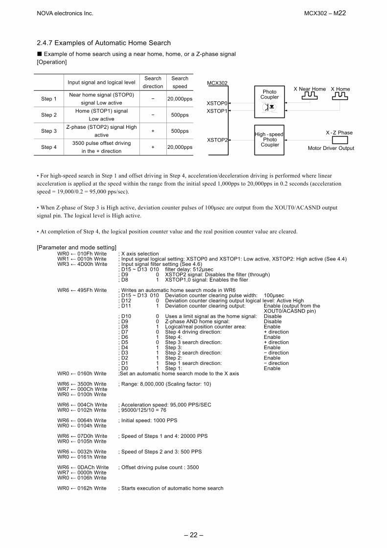
2.4.7 Examples of Automatic Home Search Example of home search using a near home, home, or a Z-phase signal
[Operation]
Input signal and logical level Search
directionSearch speed
Step 1 Near home signal (STOP0)
signal Low active − 20,000pps
Step 2 Home (STOP1) signal
Low active − 500pps
Step 3 Z-phase (STOP2) signal High
active + 500pps
Step 4 3500 pulse offset driving
in the + direction + 20,000pps
• For high-speed search in Step 1 and offset driving in Step 4, acceleration/deceleration driving is performed where linear acceleration is applied at the speed within the range from the initial speed 1,000pps to 20,000pps in 0.2 seconds (acceleration speed = 19,000/0.2 = 95,000 pps/sec). • When Z-phase of Step 3 is High active, deviation counter pulses of 100μsec are output from the XOUT0/ACASND output signal pin. The logical level is High active. • At completion of Step 4, the logical position counter value and the real position counter value are cleared. [Parameter and mode setting]
WR0 ← 010Fh Write ; X axis selection WR1 ← 0010h Write ; Input signal logical setting: XSTOP0 and XSTOP1: Low active, XSTOP2: High active (See 4.4) WR3 ← 4D00h Write ; Input signal filter setting (See 4.6) ; D15 ~ D13 010 filter delay: 512μsec ; D9 0 XSTOP2 signal: Disables the filter (through) ; D8 1 XSTOP1,0 signal: Enables the filer WR6 ← 495Fh Write ; Writes an automatic home search mode in WR6 ; D15 ~ D13 010 Deviation counter clearing pulse width: 100μsec ; D12 0 Deviation counter clearing output logical level: Active High
; D11 1 Deviation counter clearing output: Enable (output from the XOUT0/ACASND pin)
; D10 0 Uses a limit signal as the home signal: Disable ; D9 0 Z-phase AND home signal: Disable ; D8 1 Logical/real position counter area: Enable ; D7 0 Step 4 driving direction: + direction ; D6 1 Step 4: Enable ; D5 0 Step 3 search direction: + direction ; D4 1 Step 3: Enable ; D3 1 Step 2 search direction: − direction ; D2 1 Step 2: Enable ; D1 1 Step 1 search direction: − direction ; D0 1 Step 1: Enable WR0 ← 0160h Write ;Set an automatic home search mode to the X axis WR6 ← 3500h Write ; Range: 8,000,000 (Scaling factor: 10) WR7 ← 000Ch Write WR0 ← 0100h Write WR6 ← 004Ch Write ; Acceleration speed: 95,000 PPS/SEC WR0 ← 0102h Write ; 95000/125/10 = 76 WR6 ← 0064h Write ; Initial speed: 1000 PPS WR0 ← 0104h Write WR6 ← 07D0h Write ; Speed of Steps 1 and 4: 20000 PPS WR0 ← 0105h Write WR6 ← 0032h Write ; Speed of Steps 2 and 3: 500 PPS WR0 ← 0161h Write WR6 ← 0DACh Write ; Offset driving pulse count : 3500 WR7 ← 0000h Write WR0 ← 0106h Write WR0 ← 0162h Write ; Starts execution of automatic home search
XSTOP0XSTOP1
XSTOP2
X Near Home X Home
X -Z Phase
PhotoCoupler
MCX302
Motor Driver Output
High -speedPhoto
Coupler
NOVA electronics Inc. MCX302 – M23
– 23 –
After start of the execution, the function monitors the RR0-D8 (X-HOM) bit and terminates automatic home search if the bit is reset to 0 from 1. If automatic home search did not terminate normally due to an error, the RR0-D4(X-ERR) bit is set to 1 after termination. Analyze the error based on the contents of the XRR2-D7, bits D5 to D0, and bits XRR1-D15 to D12.
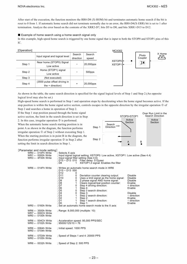
Example of home search using a home search signal only In this example, high-speed home search is triggered by one home signal that is input to both the STOP0 and STOP1 pins of this IC. [Operation]
Input signal and logical level Search
directionSearch speed
Step 1 Near home (STOP0) Signal
Low active − 20,000pps
Step 2 Home (STOP1) signal
Low active − 500pps
Step 3 (Not executed)
Step 4 (3500 pulse offset driving in
the + direction) + 20,000pps
As shown in the table, the same search direction is specified for the signal logical levels of Step 1 and Step 2.(An opposite logical level may also be set.) High-speed home search is performed in Step 1 and operation stops by decelerating when the home signal becomes active. If the stop position is within the home signal active section, controls escapes in the opposite direction by the irregular operation of Step 2 and searches a home in operation of Step 2. If the Step 1 stop position passed through the home signal active section, the limit in the search direction is set in Step 2. In this case, irregular operation is performed. When the automatic home search starting position is in point A as shown in the diagram, the function performs irregular operation of Step 2 without executing Step 1. When the starting position is in point B in the diagram, the function performs irregular operation in Step 2 after setting the limit in search direction in Step 1. [Parameter and mode setting]
WR0 ← 010Fh Write ; Selects X axis WR1 ← 0000h Write ; Input signal logical setting: XSTOP0: Low active, XSTOP1: Low active (See 4.4) WR3 ← 4F00h Write ; Input signal filter setting (See 4.6) ; D15 ~ D13 010 Filter delay: 512μsec ; D8 1 XSTOP1,0 signal: Enables the filter WR6 ← 014Fh Write ; Writes an automatic home search mode in WR6 ; D15 ~ D13 000 ; D12 0 ; D11 0 Deviation counter clearing output: Disable ; D10 0 Uses a limit signal as the home signal: Disable ; D9 0 Z-phase signal AND home signal: Disable ; D8 1 Clears logical/real position counter: Enable ; D7 0 Step 4 driving direction: + direction ; D6 1 Step 4: Enable ; D5 0 Step 3 search direction: ; D4 0 Step 3: Disable ; D3 1 Step 2 search direction: − direction ; D2 1 Step 2: Enable ; D1 1 Step 1 search direction: − direction ; D0 1 Step 1: Enable WR0 ← 0160h Write ; Set an automatic home search mode to the X axis WR6 ← 3500h Write ; Range: 8,000,000 (multiple: 10) WR7 ← 000Ch Write WR0 ← 0100h Write WR6 ← 004Ch Write ; Acceleration speed: 95,000 PPS/SEC WR0 ← 0102h Write ; 95000/125/10 = 76 WR6 ← 0064h Write ; Initial speed: 1000 PPS WR0 ← 0104h Write WR6 ← 07D0h Write ; Speed of Steps 1 and 4: 20000 PPS WR0 ← 0105h Write WR6 ← 0032h Write ; Speed of Step 2: 500 PPS
XSTOP0XSTOP1
PhotoCoupler
MCX302X Home
ActiveSection
STOP0=STOP1
SearchDirection
Over Run Limit in theSearch Direction
Step 1
Step 2A B
ActiveSection
NOVA electronics Inc. MCX302 – M24
– 24 –
WR0 ← 0161h Write WR6 ← 0DACh Write ; Offset driving pulse count : 3500 WR7 ← 0000h Write WR0 ← 0106h Write
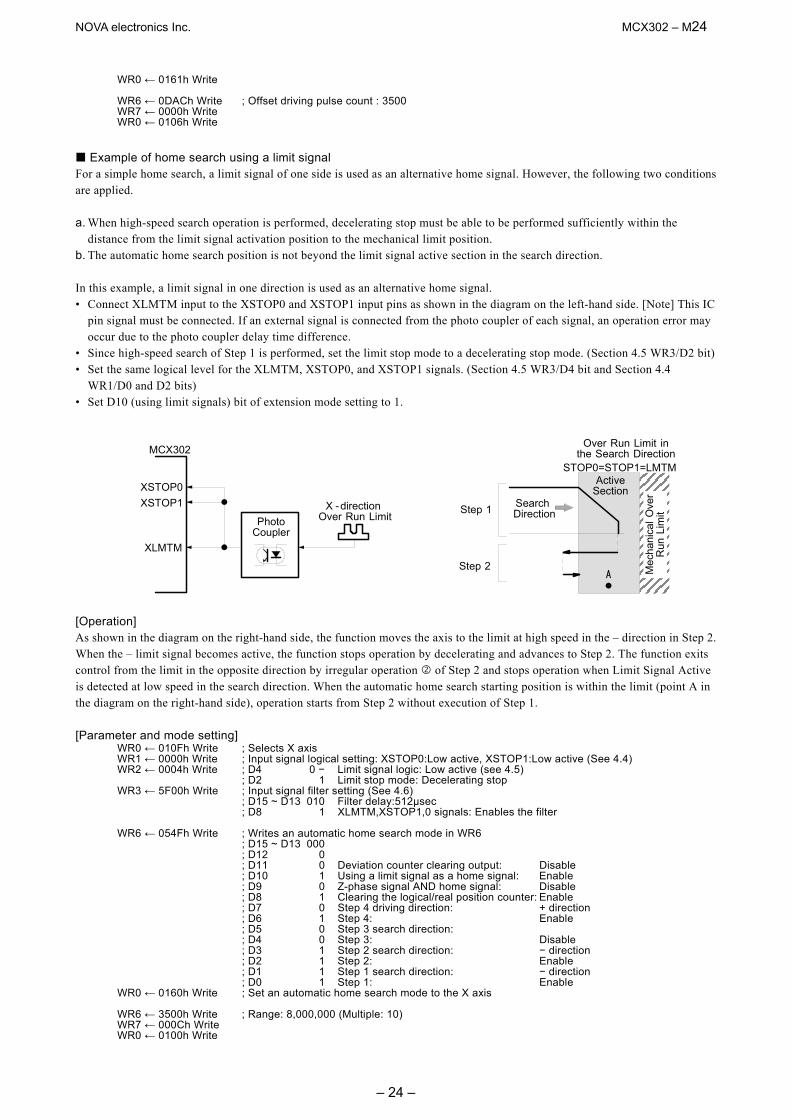
Example of home search using a limit signal For a simple home search, a limit signal of one side is used as an alternative home signal. However, the following two conditions are applied. a. When high-speed search operation is performed, decelerating stop must be able to be performed sufficiently within the
distance from the limit signal activation position to the mechanical limit position. b. The automatic home search position is not beyond the limit signal active section in the search direction. In this example, a limit signal in one direction is used as an alternative home signal. • Connect XLMTM input to the XSTOP0 and XSTOP1 input pins as shown in the diagram on the left-hand side. [Note] This IC
pin signal must be connected. If an external signal is connected from the photo coupler of each signal, an operation error may occur due to the photo coupler delay time difference.
• Since high-speed search of Step 1 is performed, set the limit stop mode to a decelerating stop mode. (Section 4.5 WR3/D2 bit) • Set the same logical level for the XLMTM, XSTOP0, and XSTOP1 signals. (Section 4.5 WR3/D4 bit and Section 4.4
WR1/D0 and D2 bits) • Set D10 (using limit signals) bit of extension mode setting to 1.
[Operation] As shown in the diagram on the right-hand side, the function moves the axis to the limit at high speed in the – direction in Step 2. When the – limit signal becomes active, the function stops operation by decelerating and advances to Step 2. The function exits control from the limit in the opposite direction by irregular operation of Step 2 and stops operation when Limit Signal Active is detected at low speed in the search direction. When the automatic home search starting position is within the limit (point A in the diagram on the right-hand side), operation starts from Step 2 without execution of Step 1. [Parameter and mode setting]
WR0 ← 010Fh Write ; Selects X axis WR1 ← 0000h Write ; Input signal logical setting: XSTOP0:Low active, XSTOP1:Low active (See 4.4) WR2 ← 0004h Write ; D4 0 − Limit signal logic: Low active (see 4.5) ; D2 1 Limit stop mode: Decelerating stop WR3 ← 5F00h Write ; Input signal filter setting (See 4.6) ; D15 ~ D13 010 Filter delay:512μsec ; D8 1 XLMTM,XSTOP1,0 signals: Enables the filter WR6 ← 054Fh Write ; Writes an automatic home search mode in WR6 ; D15 ~ D13 000 ; D12 0 ; D11 0 Deviation counter clearing output: Disable ; D10 1 Using a limit signal as a home signal: Enable ; D9 0 Z-phase signal AND home signal: Disable ; D8 1 Clearing the logical/real position counter: Enable ; D7 0 Step 4 driving direction: + direction ; D6 1 Step 4: Enable ; D5 0 Step 3 search direction: ; D4 0 Step 3: Disable ; D3 1 Step 2 search direction: − direction ; D2 1 Step 2: Enable ; D1 1 Step 1 search direction: − direction ; D0 1 Step 1: Enable WR0 ← 0160h Write ; Set an automatic home search mode to the X axis WR6 ← 3500h Write ; Range: 8,000,000 (Multiple: 10) WR7 ← 000Ch Write WR0 ← 0100h Write
XSTOP0XSTOP1 X -direction
Over Run Limit
XLMTM
MCX302
STOP0=STOP1=LMTM
A
PhotoCoupler
Step 1
Step 2
Over Run Limit inthe Search Direction
SearchDirection
ActiveSection
Mec
hani
calO
ver
Run
Lim
it
NOVA electronics Inc. MCX302 – M25
– 25 –
WR6 ← 004Ch Write ; Acceleration speed: 95,000 PPS/SEC WR0 ← 0102h Write ; 95000/125/10 = 76 WR6 ← 0064h Write ; Initial speed: 1000 PPS WR0 ← 0104h Write WR6 ← 07D0h Write ; Speed of Steps 1 and 4: 20000 PPS WR0 ← 0105h Write WR6 ← 0032h Write ; Speed of Step 2: 500 PPS WR0 ← 0161h Write WR6 ← 0DACh Write ; Offset driving pulse count: 3500 WR7 ← 0000h Write WR0 ← 0106h Write
[Notes on using limit signals] • The same search direction must be applied for Steps 1 and 2. For Step 3 (Z-phase search), apply a direction opposite to the
direction of Steps 1 and 2. For Step 4 also (offset driving), apply a direction opposite to Steps 1 and 2 and make sure that automatic home search operation stops at the position beyond the limit active section.
• When Step 3 operation is performed, the AND condition between a Z-phase signal and a home signal (STOP1) cannot be applied. The automatic home search mode bit D9 (SAND) must be set to 0.
NOVA electronics Inc. MCX302 – M26
– 26 –
2.5 Interrupt The interrupt is generated from X, Y axis. There is only one interrupt signal, INTN (33), to the host CPU. So, the signal will be OR calculated, then output, as shown in Fig. 2.25.
X Axis
Y Axis INT INT
INTN (33)
Fig. 2.24 Interrupt Signal Path in IC
Every interrupt can be enabled or disabled individually. When resetting, all interrupt signals are disabled.
Interrupt of X and Y Axes The following table shows the interrupt factors generated by X and Y axes.
Enable / Disable nWR1 Register
Status nRR3 Register
The Factors of Interrupt Happening
D9 (P≥C−) D1 (P≥C−) once the value of logical / real position counter is larger than or equal to the value of COMP− register (CM)...
D10 (P<C−) D2 (P<C−) once the value of logical/real position counter is smaller than the value ofCOMP− register (CM)...
D11 (P<C+) D3 (P<C+) once the value of logical / real position counter is larger than the value of COMP+ register (CM)…
D12 (P≥C+) D4 (P≥C+) once the value of logical / real position counter is smaller than or equal to thevalue of COMP+ register (CM)...
D13 (C-END) D5 (C-END) in the acceleration / deceleration driving, when the driving changes from theconstant speed region into the decelerating region...
D14 (C-STA) D6 (C-STA) in the acceleration / deceleration driving, when the driving changes from theaccelerating region into the constant speed region…
D15 (D-END) D7 (D-END) when the driving is finished... Each factor of interrupt can be masked by setting levels in nWR1 register bits: 1- enable and 0 - disable. When interrupt is generated during the driving, and if the interrupt is generated, each bit in nRR3 will be set to 1; INTN will be on the Low level. After the nRR3 status has been read from the host CPU, nRR3 will be cleared from 1 to 0, and INTN will return to the High-Z level.
NOVA electronics Inc. MCX302 – M27
– 27 –
2.6 Other Functions
2.6.1 Driving By External Pulses Fixed driving and continuous driving can be controlled by either commands or external signals, which can reduce the load of host CPU. By inputting an encoder 2-phase signal of MPG, jog feed of each axis is enabled. Each axis has two input signals, nEXPP and nEXPM. In fixed drive mode and a continuous drive mode, the nEXPP signal triggers driving in the + direction and the nEXPM signal in the – direction. nEXPP controls + direction pulse output, and nEXPM controls – direction command. D3 and D4 bits of register WR3 are for the setting in driving. The user should preset the parameters and commands. The default level of nEXPP and nEXPM is normally set on Hi. In MPG mode, the A-phase signal is connected to nEXPP input and the B-phase signal to nEXPM input.
Fixed Driving Mode Set bits D4 and D3 of register WR3 to 1 and 0 respectively, and set all the parameters of fixed driving. Once nEXPP is falling down to the Low level (↓), the + direction fixed driving will start; once nEXPM is raising to the Hi level (↓), the − direction fixed driving will start. The width of Low level signal must be larger than 4 CLK-cycle. Before this driving is finished, a new Hi-to-Low level falling down of the signal is invalid.
XEXPP
XEXPM
XPP
XPM
Fig. 2. 25 Example of The Constant Driving by External Signal Continuous Driving Mode
Set bits D4 and D3 of WR3 register to be 0 and 1 respectively, and set all the parameters of continuous driving. Once nEXPP is falling down to the Low level (↓), the + direction continuous driving will start; once nEXPM is raising to the Low level (↓), the − direction continuous driving will start. When nEXPP and nEXPM returns to the Hi level from the Low level, the decelerating stop will be performed in trapezoidal driving, and the sudden stop in constant speed driving.
XEXPP
XEXPM
XPP
XPM
Fig. 2. 26 Example of The Continuous Driving by External Signal
Low period
Low period
NOVA electronics Inc. MCX302 – M28
– 28 –
MPG mode
Set the bits D4 and D3 of the WR3 register to 1 and set the necessary speed parameter for driving and the output pulse number. Connect the A-phase signal of the encoder to nEXPP input and the B-phase signal to nEXPM input. The − fixed driving is activated when the nEXPM signal is at a Low level and the nEXPP signal is at the rising edge. When the output pulse number is set to 1, one drive pulse is output at each of the rising edge and falling edge of the nEXPP signal. If the output pulse number is set to P, the P number of drive pulses is output. Set the speed parameter in the following conditions to complete output of all the P number of drive pulses with a period from the rising edge/falling edge of the nEXPP signal to the next rising edge/falling edge. V ≥ F × P × 2 V : Drive speed (pps) P : Output pulses
F : Frequency (Hz) at the maximum speed of MPG encoder
For instance, under the condition where the maximum frequency of the MPG is F=500Hz and the output pulse is P=1, the drive speed must be V=1000PPS or greater. Since acceleration/deceleration driving is not applied, set the initial speed SV to the same value as the drive speed. However, when a stepping motor is used for driving, the drive speed must not exceed the automatic activation frequency of the motor.
2.6.2 Pulse Output Type Selection There are two types of pulse output--independent 2-pulse type: when the driving is in + direction, the pulse output is from nPP/PLS; when the driving is in − direction, the pulse output is from nPM/DIR; 1-pulse 1- direction type: nPP/PLS is for pulse outputting, and nPM/DIR is for direction signal outputting. (pulse / direction is set on the positive logical level)
Pulse Output Waveform Pulse Output Type Drive Direction
nPP/PLS Signal nPM/DIR Signal
+Direction Low level
Independent 2-pulse −Direction Low level
+Direction Low level
1-pulse 1-direction −Direction
Bit D6 (PLSMD) of register WR2 is used for the selection of pulse output type. Additionally, bits D7 (PLS-L) and D8 (DIR-L) of register WR2 can be used for pulse outputting, direction and logical level setting.
Hi level
XEXPP(A phase)
XEXPM(B phase)
XPP
XPM
Fig. 2.27 Example Output Pulse 1Driving by A MPG
Normal rotation Reverse rotation
XEXPP(A phase)
XEXPM(B phase)
XPP
XPM
Fig. 2.28 Example of Output Pulse 2 Driving by A MPG
Normal rotation Reverse rotation
NOVA electronics Inc. MCX302 – M29
– 29 –
[Note] Please refer to Chapter 13.2, 13.3 for the pulse signal (nPLS) and direction signal (nDIR) in 1- pulse 1-direction pulse outputting.
2.6.3 Pulse Input Type Selection For real position counter, A/B quadrature pulse type and Up / Down pulse type can be selected for pulse input.
A/B quadrature pulse input mode A/B quadrature pulse input mode can be set by setting the D9 (PINMD) bit of the WR2 register to 0. In this mode at the time of reset (WR1/D7=0), when A phase is advancing with positive logical pulses, the count is incremented and when the B-phase is advancing, the count is decremented. The count is incremented and decremented at the rising edge and falling edge of both signals. When the real position counter up/down reverse bit (WR1/D7) is set to 1, the up/down operation of the real counter is reversed. In A/B quadrature pulse input mode, the input pulses can be divided into 1/2 or 1/4.
nECA/PPIN
nECB/PMIN
EPINV)= 0
EPINV)= 1
Count up at the both signals
Count down at the both signals
Count down at the both signals
Count up at the both signals
Up/down pulse input mode By setting the D9 (PINMD) bit of the WR2 register to 1, a counter up/down pulse input mode can be set. nECA/PPIN is count up input and nECB/PMIN is count down input. The counter counts at the rising edge of the positive pulse.
nECA/PPIN
nECB/PMINCount up Count down
Use the D9 (PINMD) bit of the WR2 register for selecting a pulse input mode and the D11 and D10 (PIND1,0) bits to set the division ratio of encoder 2-phase pulse input. [Note] Time specification is applied to the pulse width and pulse cycle of input pulses. See Section 12.2.5 Input Pulse of Chapter 12.
2.6.4 Hardware Limit Signals Hardware limit signals, nLMTP and nLMTM, are used for stopping the pulse output if the limit sensors of + and − directions are triggered. When the limit signal and also the logical level are active, the command of sudden stop or decelerating stop can be set by bits D3 and D4 (HLMT+, HLMT−), and D2 (LMTMD) of register WR2.
2.6.5 Interface to Servo Motor Drivers Enable / Disable and logical levels of the input signals for connecting servo motor drivers such as nINPOS (in-position input signal) and nALARM (alarm input signal) can be set by D15~12 bits of register WR2. nINPOS input signal responds to the in-position signal of servo motor driver. When “enable” is set, and when the driving is finished, nINPOS will wait for the “active”. Then, the n-DRV bit of main status register RRO will return to 0. nALARM input signal receives the alarm signal from servo motor drivers. When “enable” is set, nALARM signal will be monitored, and the D4 (alarm) bit of RR2 register is 1 when nALARM is active. The sudden stop will occur in the driving when this signal is active. These input signals from servo motor drivers can be read by RR4 and RR5 registers.
NOVA electronics Inc. MCX302 – M30
– 30 –
2.6.6 Emergency Stop Signal EMGN is able to perform the emergency stop function for both X and Y axes during the driving. Normally, this signal is kept on the Hi level. When it is falling to the Low level, all axes will stop immediately, and the D5 (EMG) bit of register RR2 (each axis) becomes 1. Please be noted that there is no way to select the logical level of EMGN signal. Please check the following methods to perform the emergency stop function from the host CPU.
a. Execute the sudden stop commend for both of 2 axes at the same time… Appoint both X and Y axes, then write the sudden stop command (27h) to register WR0.
b. Reset software limit…
Write 800h to register WR0 to reset software limit.
2.6.7 Status Output The driving status of each axis will be output to main status register RR0 and status register nRR1 of each axis, also it can be output as signal that shares the same terminal with general purpose output signals. D7 (OUTSL) bit of register WR3 should be set 1 for drive status output. This bit will return 0 by reset and then turn to the terminal for general purpose output (nOUT 7~0). nOUT4/DRIVE output signals and bits D1, 0 (n-DRV) of register RR0 can be used for drive / stop status output. The driving status of acceleration / constant speed / deceleration will be output to bits D2 (ASND), D3 (CNST) and D4 (DSND), and also the signals TS/ASND, nOUT6/CNST and nOUT7/DSND will show the levels. Moreover in S curve acceleration / deceleration driving, the state of acceleration / constant speed / deceleration will be also shown to bits D5 (AASND), D6 (ACNST) and D7 (ADSND) and the signals nOUT0/ACASND and nOUT1/ACDSND. However, if deviation counter clearing is enabled in automatic home search mode setting, nOUT0/ACASND functions as deviation counter clearing output, so nOUT0/ACASND cannot be used. See section 2.6.7 and 2.6.8.
Drive Status Status Register
( Active : 1 ) Output Signal ( Active : Hi )
Drive RR0 / D1, 0 (n-DRV) nDRIVE Acceleration nRR1 / D2 (ASND) nASND
Constant Speed nRR1 / D3 (CNST) nCNST Deceleration nRR1 / D4 (DSND) nDSND
Acceleration / Deceleration Increase nRR1 / D5 (AASND) nACASND Acceleration / Deceleration Constant nRR1 / D6 (ACNST) - Acceleration / Deceleration Decrease nRR1 / D7 (ADSND) nACDSND
Stop Acceleration
Speed
time
StopDecelerationConstantSpeed
Speed
0
Acceleration/DecelerationIncrease
Acceleration ConstantAcceleration/Deceleration
Decrease
AccelerationConstantSpeed Deceleration
time
Acceleration/Deceleration
Linear acceleration driving state
S curve acceleration driving state
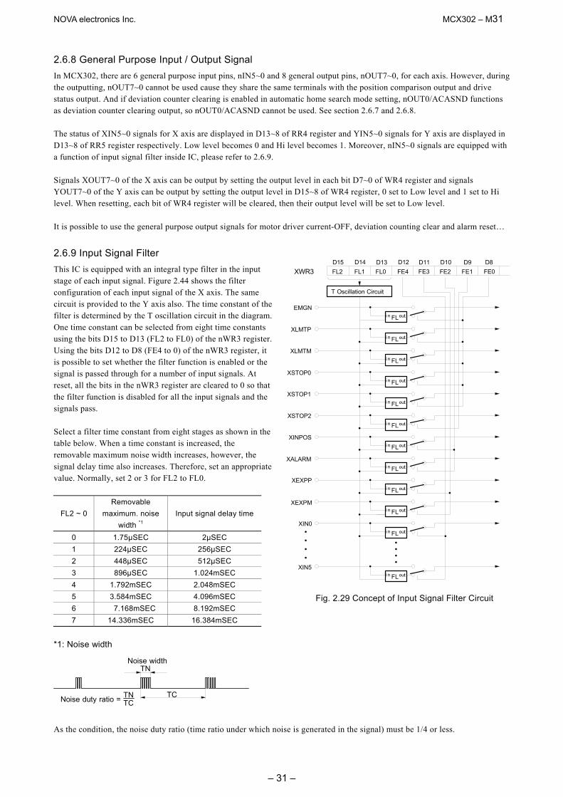
NOVA electronics Inc. MCX302 – M31
– 31 –
2.6.8 General Purpose Input / Output Signal In MCX302, there are 6 general purpose input pins, nIN5~0 and 8 general output pins, nOUT7~0, for each axis. However, during the outputting, nOUT7~0 cannot be used cause they share the same terminals with the position comparison output and drive status output. And if deviation counter clearing is enabled in automatic home search mode setting, nOUT0/ACASND functions as deviation counter clearing output, so nOUT0/ACASND cannot be used. See section 2.6.7 and 2.6.8. The status of XIN5~0 signals for X axis are displayed in D13~8 of RR4 register and YIN5~0 signals for Y axis are displayed in D13~8 of RR5 register respectively. Low level becomes 0 and Hi level becomes 1. Moreover, nIN5~0 signals are equipped with a function of input signal filter inside IC, please refer to 2.6.9. Signals XOUT7~0 of the X axis can be output by setting the output level in each bit D7~0 of WR4 register and signals YOUT7~0 of the Y axis can be output by setting the output level in D15~8 of WR4 register, 0 set to Low level and 1 set to Hi level. When resetting, each bit of WR4 register will be cleared, then their output level will be set to Low level. It is possible to use the general purpose output signals for motor driver current-OFF, deviation counting clear and alarm reset…
2.6.9 Input Signal Filter This IC is equipped with an integral type filter in the input stage of each input signal. Figure 2.44 shows the filter configuration of each input signal of the X axis. The same circuit is provided to the Y axis also. The time constant of the filter is determined by the T oscillation circuit in the diagram. One time constant can be selected from eight time constants using the bits D15 to D13 (FL2 to FL0) of the nWR3 register. Using the bits D12 to D8 (FE4 to 0) of the nWR3 register, it is possible to set whether the filter function is enabled or the signal is passed through for a number of input signals. At reset, all the bits in the nWR3 register are cleared to 0 so that the filter function is disabled for all the input signals and the signals pass. Select a filter time constant from eight stages as shown in the table below. When a time constant is increased, the removable maximum noise width increases, however, the signal delay time also increases. Therefore, set an appropriate value. Normally, set 2 or 3 for FL2 to FL0.
FL2 ~ 0 Removable
maximum. noise width *1
Input signal delay time
0 1.75μSEC 2μSEC
1 224μSEC 256μSEC
2 448μSEC 512μSEC
3 896μSEC 1.024mSEC
4 1.792mSEC 2.048mSEC
5 3.584mSEC 4.096mSEC
6 7.168mSEC 8.192mSEC
7 14.336mSEC 16.384mSEC
*1: Noise width
As the condition, the noise duty ratio (time ratio under which noise is generated in the signal) must be 1/4 or less.
EMGN
XLMTP
XLMTM
XSTOP2
XSTOP1
XSTOP0
XINPOS
XALARM
XEXPP
XEXPM
XIN5
XIN0
FLi n out
FLi n out
FLi n out
FLi n out
FLi n out
FLi n out
FLi n out
FLi n out
FLi n out
FLi n out
FLi n out
FLi n out
D15 D14 D13 D12 D11 D10 D9 D8FL2 FL1 FL0 FE4 FE3 FE2 FE0FE1XWR3
T Oscillation Circuit
Fig. 2.29 Concept of Input Signal Filter Circuit
Noise widthTN
TCNoise duty ratio = TNTC
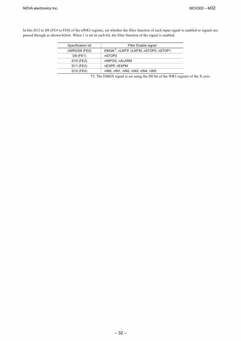
NOVA electronics Inc. MCX302 – M32
– 32 –
In bits D12 to D8 (FE4 to FE0) of the nWR3 register, set whether the filter function of each input signal is enabled or signals are passed through as shown below. When 1 is set in each bit, the filter function of the signal is enabled.
Specification bit Filter Enable signal nWR3/D8 (FE0) EMGN*2, nLMTP, nLMTM, nSTOP0, nSTOP1
D9 (FE1) nSTOP2 D10 (FE2) nINPOS, nALARM
D11 (FE3) nEXPP, nEXPM
D12 (FE4) nIN0, nIN1, nIN2, nIN3, nIN4, nIN5 *2: The EMGN signal is set using the D8 bit of the WR3 register of the X axis.
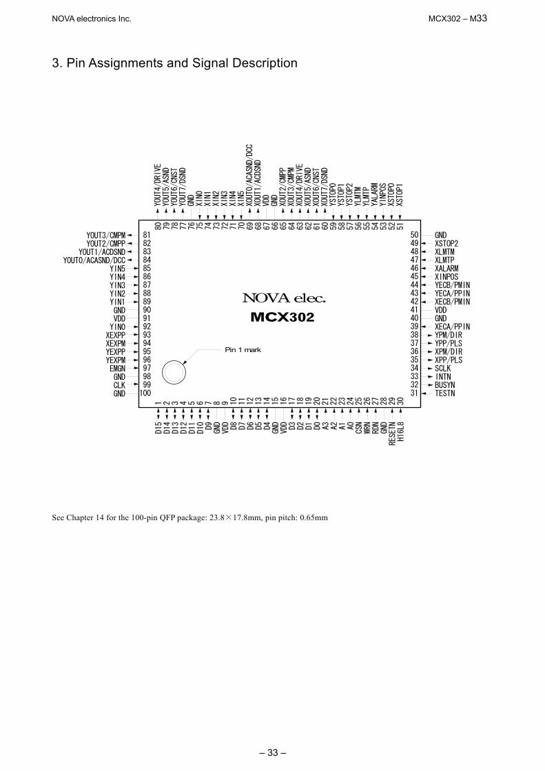
NOVA electronics Inc. MCX302 – M33
– 33 –
3. Pin Assignments and Signal Description
1 2 3 4 5 6 7 8 9 10 11 12 13 14 15 16 17 18 19 20 21 22 23 24 25 26 27 28 29 30
5049484746454443424140393837363534333231
81828384858687888990919293949596979899100
YOUT3/CMPMYOUT2/CMPP
YOUT1/ACDSNDYOUT0/ACASND/DCC
YIN5YIN4YIN3YIN2YIN1GNDVDDYIN0XEXPPXEXPMYEXPPYEXPMEMGNGNDCLKGND
NOVAelec.
MCX302
Pin 1 mark
D15
D14
D13
D12
D11
D10 D9 GND
VDD D8 D7 D6 D5 D4 GND
VDD D3 D2 D1 D0 A3 A2 A1 A0 CSN
WRN
RDN
GND
RESETN
H16L8
80 79 78 77 76 75 74 73 72 71 70 69 68 67 66 65 64 63 62 61 60 59 58 57 56 55 54 53 52 51
YOUT4/DRIVE
YOUT5/ASND
YOUT6/CNST
YOUT7/DSND
GND
XIN0
XIN1
XIN2
XIN3
XIN4
XIN5
XOUT0/ACASND/DCC
XOUT1/ACDSND
VDD
GND
XOUT2/CMPP
XOUT3/CMPM
XOUT4/DRIVE
XOUT5/ASND
XOUT6/CNST
XOUT7/DSND
YSTOP0
YSTOP1
YSTOP2
YLMTM
YLMTP
YALARM
YINPOS
XSTOP0
XSTOP1
GNDXSTOP2XLMTMXLMTPXALARMXINPOSYECB/PMINYECA/PPINXECB/PMINVDDGNDXECA/PPINYPM/DIRYPP/PLSXPM/DIRXPP/PLSSCLKINTNBUSYNTESTN
See Chapter 14 for the 100-pin QFP package: 23.8×17.8mm, pin pitch: 0.65mm
NOVA electronics Inc. MCX302 – M34
– 34 –
Signal Description Signals X and Y are input / output signals for X and Y axes, where n stands for X and Y. If the signals are named
N, they are negative-active or low-active. See the end of this chapter for description of input/output circuits. An integral filter circuit is available in the internal input column of this IC for the input signals with – F – symbol. See Section 2.6.9 for the filter function.
Signal Name Pin No. Input/Output Signal Description CLK 99 Input A Clock: clock signal for internal synchronous loop of MCX302
The standard frequency is 16 MHz. This signal is for drive speed, acceleration / deceleration and jerk. If the frequency setting is not 16 MHz, the setting values of speed and acceleration / deceleration are different.
D15~D0 1~7,10~ 14, 17~20
Bi-directional A DATA BUS: 3-state bi-direction 16-bit data bus When CSN=Low and RDN=Low, these signals are for outputting. Otherwise, they are high impedance inputs. If 8-bit data bus is used, D15~D8 can not be used, and D15~D8 should be pull up to + 5V through high impedance (about 100 kΩ).
A3~A0 21,22,23,24
Input A Address: address signal for host CPU to access the write / read registers A3 is used only when the 8-bit data bus is used.
CSN 25 Input A Chip Select: input signal for selecting I/O device for MCX302. Set CSN to the Low level for data reading and writing.
WRN 26 Input A Write Strobe: its level is Low while data is being written to MCX302. When WRN is Low, CSN and A3-A0 must be assured. When WRN is up (↑), the data will be latched in the write register, and while WRN is up (↑), the levels of D15~D0 should be assured.
RDN 27 Input A Read Strobe: its level is Low while data is being read from MCX302. Only when CSN is on the low level, the selected read register data from A3~A0 address signals can be output from the data bus.
RESETN 29 Input A Reset: reset (return to the initial setting) signal for MCX302. Setting RESETN to Low for more than 4 CLK cycles will reset MCX302. The RESETN setting is necessary when the power is on. [Note] If there is no clock input to MCX302, setting the RESETN to Low still cannot reset this IC.
H16L8 30 Input A Hi=16-bit, Low=8-bit: data bus width selection for 16-bit / 8-bit When the setting is Hi, 16-bit data bus is selected for processing the 16-bit data reading / writing in IC; when the setting is Low, 8-bit data bus (D7~D0) is active for data reading / writing.
TESTN 31 Input A Test: terminal for internal-circuit test Please open, or connect it to + 5V.
BUSYN 32 Output B Busy: reflecting the execution of the input command at this moment Once the command is written to MCX302, the process will take 2 CLK to 4CLK (250nsec for 16MHz) on the Low level. When BUSYN is on the Low level, the other written commands cannot be executed.
INTN 33 Output B Interrupt: outputting an interrupt signal to the host CPU. If any interrupt factor occurs the interrupt, the level is Low; when the interrupt is released, it will return to the Hi-Z level.
SCLK 34 Output A System Clock: SCLK=CLK/2 All the signals in MCX302 are controlled and synchronized by internal SCLK. When the output signal of each axis is latched, it can be used as an external signal source. [Note] There is no SCLK output when RESETN is on the Low level.
XPP/PLS YPP/PLS
35 37
Output A Pulse +/Pulse: + direction dive pulse outputting When the reset is on the Low level, and while the driving is starting, DUTY 50% (at constant speed) of the plus drive pulses are outputting. + or − pulse mode is selectable. When the 1-pulse 1-direction mode is selected, this terminal is for drive output.
XPM/DIR YPM/DIR
36 38
Output A Pulse −/Pulse: − direction dive pulse outputting When the reset is on the Low level, and while the driving is starting, DUTY 50% (at constant speed) of the plus drive pulses are outputting. + or − pulse mode is selectable. When the 1-pulse 1-direction mode is selected, this terminal is direction signal.
XECA/PPIN YECA/PPIN
39 43
Input A Encoder−A/Pulse +in: signal for encoder phase-A input This input signal, together with phase-B signal, will make the Up / Down pulse transformation to be the input count of real position counter. When the Up / Down pulse input mode is selected, this terminal is for UP pulses input. Once the input pulse is up (↑), the real position counter is counting up.
XECB/PMIN YECB/PMIN
42 44
Input A Encoder-B/Pulse -in: signal for encoder phase-B input This input signal, together with phase-A signal, will make the Up / Down pulse transformation to be the input count of real position counter. When the Up / Down pulse input mode is selected, this terminal is for DOWN pulses input. Once the input pulse is up (↑), the real position counter is counting down.
NOVA electronics Inc. MCX302 – M35
– 35 –
Signal Name Pin No. Input/Output Signal Description XINPOS YINPOS
45 53
Input A − F −
In-position: input signal for servo driver in-position Enable / disable and logical levels can be set as commands. When “enable” is set, and after the driving is finished, this signal is active and standby. n-DVR bit of main status register returns to 0.
XALARM YALARM
46 54
Input A − F −
Servo Alarm: input signal for servo driver alarm Enable / disable and logical levels can be set as commands. When it is enable and when this signal is in its active level, the ALARM bit of RR2 register becomes 1.
XLMTP YLMTP
47 55
Input A − F −
OVER Limit +: signal of + direction over limit During the + direction drive pulse outputting, decelerating stop or sudden stop will be performed once this signal is active. When the filter function is disabled, the active pulse width must be 2CLK or more. When it is enable, and when this signal is in its active level, the HLMT+ of RR2 register becomes 1.
XLMTM YLMTM
48 56
Input A − F −
OVER Limit −: signal of − direction over limit During the − direction drive pulse outputting, decelerating stop or sudden stop will be performed once this signal is active. The active pulse width should be more than 2CLK. Decelerating stop / sudden stop and logical levels can be set during the mode selection. When it is enable, and when this signal is in its active level, the HLMT− of RR2 register becomes 1.
XSTOP2~0 YSTOP2~0
49, 51, 5257, 58, 59
Input A − F −
STOP 2~0: input signal to perform decelerating / sudden stop for each axisThese signals can be used for HOME searching. The active pulse width should be more than 2CLK. Enable / disable and logical levels can be set for STOP2~STOP0. The signal status can be read from register RR4 / RR5. And nSTOP2 signal is equipped with a function that clears a real position counter value by (↑) signal depends on mode setting so that it is appropriate to input an encoder Z-phase signal.
XOUT7/DSND YOUT7/DSND
60 77
Output A General Output 7 / Descend: general purpose output signals XOUT7~0 can output the 1/0 data of D7~0 in WR4 register and YOUT7~0 can output the 1/0 data of D15~8 in WR4 register to Hi / Low. They become Low when the IC is reset. When the drive status output mode is engaged, this signal can be used for reflecting the status of deceleration. While the driving command is executed and during the deceleration, it becomes Hi.
XOUT6/CNST YOUT6/CNST
61 78
Output A General Output 6 / Constant: general purpose output signals (the operation is as same as nOUT7) When the drive status output mode is engaged, this signal can be used for reflecting the status of constant speed drive. While the driving command is executed and during the constant speed drive, it becomes Hi.
XOUT5/ASND YOUT5/ASND
62 79
Output A General Output 5 / Ascend: general purpose output signals (the operation is as same as nOUT7) When the drive status output mode is engaged, this signal can be used for reflecting the status of acceleration. While the driving command is executed and during the acceleration, it becomes Hi.
XOUT4/DRIVE YOUT4/DRIVE
63 80
Output A General Output 4 / Drive: general purpose output signals (the operation is as same as nOUT7) When the drive status output mode is engaged, this signal can be used for reflecting the status of drive. During outputting drive pulses, it becomes Hi. The DRIVE signal is set to a High level until nINPOS becomes active, while the nINPOS signal for the serve motor is enabled by mode selection.
XOUT3/CMPM YOUT3/CMPM
64 81
Output A General Output 3 / Compare−: general purpose output signals (the operation is as same as nOUT7) When the drive status output mode is engaged, it becomes Hi if the value of logical / real position counter is smaller than that of COMP−; it becomes Low if the value of logical / real position counter is larger than that of COMP−.
XOUT2/CMPP YOUT2/CMPP
65 82
Output A General Output2 / Compare+: general purpose output signals (the operation is as same as nOUT7) When the drive status output mode is engaged, it becomes Hi if the value oflogical / real position counter is larger than that of COMP+; it becomes Low if the value of logical / real position counter is smaller than that of COMP+.
XOUT1/ACDSND YOUT1/ ACDSND
68 83
Output A General Output 1 / Acceleration Descend: general purpose output signals(the operation is as same as nOUT7) When the drive status output mode is engaged, it becomes Hi if acceleration / deceleration of S curve acceleration / deceleration decreases.
XOUT0/ACASND /DCC
YOUT0/ ACASND /DCC
69 84
Output A General Output 0 / Acceleration Ascend: general purpose output signals (the operation is as same as nOUT7) When the drive status output mode is engaged, it becomes Hi if acceleration / deceleration of S curve acceleration / deceleration increases. When deviation counter clearing output is enabled in automatic home search mode setting, deviation counter clearing signal is output from this pin.
NOVA electronics Inc. MCX302 – M36
– 36 –
Signal Name Pin No. Input/Output Signal Description XIN5 YIN5
70 85
Input A − F −
General Input 5 / : general purpose input signals The status of signal is displayed in a register, XIN5~0 of the X axis is displayed in D13~8 of RR4 register and YIN5~0 of the Y axis is displayed in D13~8 of RR5 register. Low level input shows 0, High level input shows 1.
YIN4 YIN4
71 86
Input A − F −
General Input 4 / : general purpose input signals (Reading operation is as same as nIN5)
XIN3 YIN3
72 87
Input A − F −
General Input 3 / : general purpose input signals (Reading operation is as same as nIN5)
XIN2 YIN2
73 88
Input A − F −
General Input 2 / : general purpose input signals (Reading operation is as same as nIN5)
XIN1 YIN1
74 89
Input A − F −
General Input 1 /: general purpose input signals (Reading operation is as same as nIN5)
XIN0 YIN0
75 92
Input A − F −
General Input 0 /: general purpose input signals (Reading operation is as same as nIN5)
XEXPP YEXPP
93 95
Input A − F −
External Operation +: + direction drive starting signal from external sourceWhen the fixed driving is commanded from an external source, +direction driving will start if this signal is down (↓). Otherwise, when the continuous driving is commanded from an external source, + driving will start if this signal is on the Low level.
XEXPM YEXPM
94 96
Input A − F −
External Operation −: − direction drive starting signal from external sourceWhen the fixed driving is commanded from an external source, − direction driving will start if this signal is down (↓). Otherwise, when the continuous driving is commanded from an external source, − driving will start if this signal is on the Low level.
EMGN
97
Input A − F −
Emergency Stop: input signal to perform the emergency stop for all axes When this signal is on the Low level, every axis will stop the operation immediately. EMG bit of register RR2, of each axis, will become 1. The low level pulse width should be more than 2CLK. [Note] For this signal, its logical levels cannot be selected.
GND
8, 15, 28, 40, 50, 66, 76, 90, 98, 100
Ground (0V) Terminal All of the 10 pins must be connected to 0V.
VDD 9, 16, 41, 67, 91
+ 5V Power Terminal. All of the 5 pins must be connected to +5V.
Input/ Output Circuit
Input A Smith trigger input in TTL level, which is pulled up to VDD with high impedance. (dozens of kΩ ~ hundreds of kΩ) CMOS and TTL can be connected. The user should open, or pull up with + 5V if the input is not used. The signal with – F – symbol has an integral filter circuit in the internal input column of this IC. See Section 2.6.9 for the filter function.
Output A It is CMOS level output, 4mA driving buffer (Hi level output current IOH=−4mA, VOH=2.4Vmin, Low level output current IOL=4mA, VOL=0.4Vmax). Up to 10 LSTTL can be driven.
Output B It is open drain type output, 4mA driving buffer, (Low level output current IOL=4mA, VOL=0.4Vmax). Pull up to +5V with high impedance if this output is used.
Bi-directional A Input side is TTL Smith trigger. Because there is no pull high resister for those signals in this IC, the user should pull up the data bus with high impedance. The user should pull up to +5V with high impedance (about 100 kΩ) when bits D15~D8 are not used. Output side is CMOS level output, 8mA driving buffer (Hi level output current IOH=−8mA, VOH=2.4Vmin, Low level output current IOL=8mA, VOL=0.4Vmax).
Notes for the Design of Circuitry a. De-coupling Capacitor Please connect VDD and GND with one or two De-coupling capacitors (about 0.1μF). b. Noise Generated by Terminal Induction The noise will exist because the inductance is in these pins. The user can add a capacitor (10-100pF) to pins to reduce the noise. c. Reflection on Transfer Path The load capacity for outputting types A, B, and bi-direction type A and B are 20-50pf. So, the reflection will happen if the PCB wiring is more than 60cm.
NOVA electronics Inc. MCX302 – M37
– 37 –
4. Register This chapter indicates the user how to access all the registers in MCX302, and what are the mapping addresses of these registers.
4.1 Register Address by 16-bit Data Bus As shown is the table below, when 16-bit data bus is used, the access address of read / write register is 8-bit.
Write Register in 16-bit Data Bus All registers are 16-bit length.
Address A2 A1 A0
Symbol Register Name Contents
0 0 0 WR0 Command Register for setting axis assignment and command
0 0 1 XWR1 YWR1
X axis mode register 1 Y axis mode register 1
for setting the logical levels of external decelerating / sudden stop, enable / disable, the valid / invalid of interrupt for each axis, and the mode in the real position counter.
0 1 0 XWR2 YWR2
X axis mode register 2 Y axis mode register 2
for setting the limit signal mode, driving pulse mode, encoder input signal mode, the logical levels and enable / disable of servo motor signal for each axis, and the action mode in the real position counter.
0 1 1
XWR3 YWR3
X axis mode register 3 Y axis mode register 3
for setting the manual deceleration, individually decelerating, and S-curve acceleration/ deceleration mode for each axis, external operation mode, and input signal filter.
1 0 0 WR4 Output register for setting the general output nOUT7 ~ 0 1 0 1 not used
1 1 0 WR6 Data writing register 1 for setting the low word 16-bit (D15-D0) for data writing.
1 1 1 WR7 Data writing register 2 for setting the high word 16-bit (D31-D16) for data writing. Each axis is with WR1, WR2 and WR3 mode registers. Each register is for 2-axis data writing (at the same address).
Before those registers have been accessed, the host CPU should specify which axis is going to be accessed by writing a NOP command into WR0.
The bits of nWR1, nWR2, nWR3 and nWR4 will be cleared to 0 after the resetting. It will be unknown for other registers.
Read Register in 16-bit Data Bus
All registers are 16-bit length. Address
A2 A1 A0 Symbol Register Name Contents
0 0 0 RR0 Main status register error status, driving status, automatic home search running status.
0 0 1 XRR1 YRR1
X axis status register 1 Y axis status register 1
comparison result, acceleration state, and jerk state. finishing status
0 1 0 XRR2 YRR2
X axis status register 2 Y axis status register 2
error message, automatic home search execution state
0 1 1
XRR3 YRR3
X axis status register 3 Y axis status register 3
interrupt message
1 0 0 RR4 Input register 1 /O input for X axis
1 0 1 RR5 Input register 2 I/O input for Y axis
1 1 0 RR6 Data reading register 1 low word of data register (D15 ~ D0) 1 1 1 RR7 Data reading register 2 high word of data register (D31 ~ D16)
Each axis is with RR1, RR2 and RR3 mode registers. Each register is for 2-axis data writing (at the same address). Before
those registers have been accessed, the host CPU should specify which axis is going to be accessed by writing a NOP command into WR0.
NOVA electronics Inc. MCX302 – M38
– 38 –
4.2 Register Address by 8-bit Data Bus In case of the 8-bit data bus access, the 16-bit data bus can be divided into high and low word byte. As shown in the table below, xxxxL is the low word byte (D7~D0) of 16-bit register xxxx, xxxxH is the high word byte (D15~8) of 16-bit register xxxx. Only for the command register (WR0L, WR0H), the user must write to the high word byte (WR0H), then to the low word byte (WR0L).
Write Register in 8-bit Data Bus Read Register in 8-bit Data Bus Address
A3 A2 A1 A0 Write Register Address
A3 A2 A1 A0 Read Register
0 0 0 0 WR0L 0 0 0 0 RR0L 0 0 0 1 WR0H 0 0 0 1 RR0H 0 0 1 0 XWR1L,YWR1L 0 0 1 0 XRR1L,YRR1L 0 0 1 1 XWR1H,YWR1H 0 0 1 1 XRR1H,YRR1H 0 1 0 0 XWR2L,YWR2L 0 1 0 0 XRR2L,YRR2L 0 1 0 1 XWR2H,YWR2H 0 1 0 1 XRR2H,YRR2H 0 1 1 0 XWR3L,YWR3L 0 1 1 0 XRR3L,YRR3L 0 1 1 1 XWR3H,YWR3H 0 1 1 1 XRR3H,YRR3H 1 0 0 0 WR4L 1 0 0 0 RR4L 1 0 0 1 WR4H 1 0 0 1 RR4H 1 0 1 0 not used 1 0 1 0 RR5L 1 0 1 1 not used 1 0 1 1 RR5H 1 1 0 0 WR6L 1 1 0 0 RR6L 1 1 0 1 WR6H 1 1 0 1 RR6H 1 1 1 0 WR7L 1 1 1 0 RR7L 1 1 1 1 WR7H
1 1 1 1 RR7H
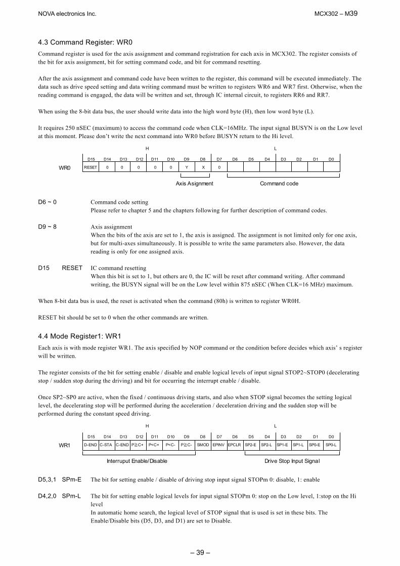
NOVA electronics Inc. MCX302 – M39
– 39 –
4.3 Command Register: WR0 Command register is used for the axis assignment and command registration for each axis in MCX302. The register consists of the bit for axis assignment, bit for setting command code, and bit for command resetting. After the axis assignment and command code have been written to the register, this command will be executed immediately. The data such as drive speed setting and data writing command must be written to registers WR6 and WR7 first. Otherwise, when the reading command is engaged, the data will be written and set, through IC internal circuit, to registers RR6 and RR7. When using the 8-bit data bus, the user should write data into the high word byte (H), then low word byte (L). It requires 250 nSEC (maximum) to access the command code when CLK=16MHz. The input signal BUSYN is on the Low level at this moment. Please don’t write the next command into WR0 before BUSYN return to the Hi level.
H L
WR0 RESET 0 Y X
D15 D14 D13 D12 D11 D10 D9 D8 D7 D6 D5 D4 D3 D2 D1 D0
0 0 0 0 0
Axis Asignment Command code
D6 ~ 0 Command code setting Please refer to chapter 5 and the chapters following for further description of command codes.
D9 ~ 8 Axis assignment
When the bits of the axis are set to 1, the axis is assigned. The assignment is not limited only for one axis, but for multi-axes simultaneously. It is possible to write the same parameters also. However, the data reading is only for one assigned axis.
D15 RESET IC command resetting
When this bit is set to 1, but others are 0, the IC will be reset after command writing. After command writing, the BUSYN signal will be on the Low level within 875 nSEC (When CLK=16 MHz) maximum.
When 8-bit data bus is used, the reset is activated when the command (80h) is written to register WR0H. RESET bit should be set to 0 when the other commands are written.
4.4 Mode Register1: WR1 Each axis is with mode register WR1. The axis specified by NOP command or the condition before decides which axis’ s register will be written. The register consists of the bit for setting enable / disable and enable logical levels of input signal STOP2~STOP0 (decelerating stop / sudden stop during the driving) and bit for occurring the interrupt enable / disable. Once SP2~SP0 are active, when the fixed / continuous driving starts, and also when STOP signal becomes the setting logical level, the decelerating stop will be performed during the acceleration / deceleration driving and the sudden stop will be performed during the constant speed driving.
SP0-L
H L
Interruput Enable/Disable
WR1
Drive Stop Input Signal
D11 D15
D-END
D14 D13 D12 D10 D9 D8 D7 D6 D5 D4 D3 D2 D1 D0
C-STA C-END P≧C+ P<C+ P<C- P≧C- SMOD EPINV EPCLR SP2-E SP2-L SP1-E SP1-L SP0-E
D5,3,1 SPm-E The bit for setting enable / disable of driving stop input signal STOPm 0: disable, 1: enable D4,2,0 SPm-L The bit for setting enable logical levels for input signal STOPm 0: stop on the Low level, 1:stop on the Hi
level In automatic home search, the logical level of STOP signal that is used is set in these bits. The
Enable/Disable bits (D5, D3, and D1) are set to Disable.
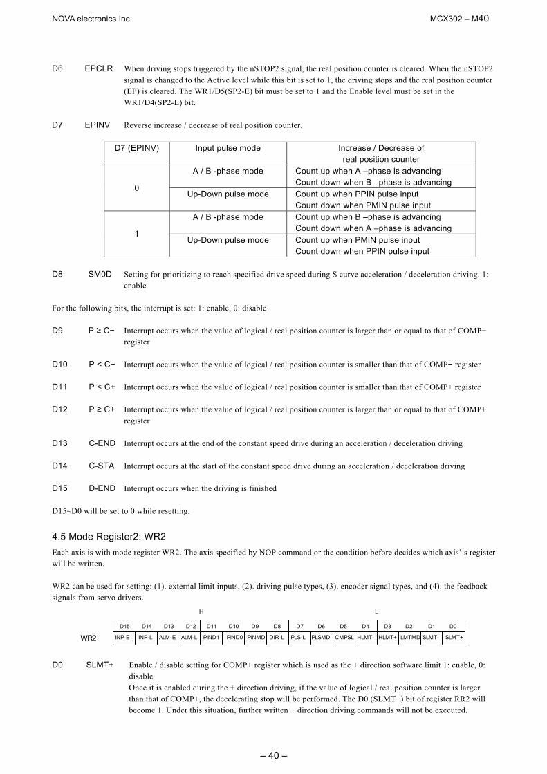
NOVA electronics Inc. MCX302 – M40
– 40 –
D6 EPCLR When driving stops triggered by the nSTOP2 signal, the real position counter is cleared. When the nSTOP2
signal is changed to the Active level while this bit is set to 1, the driving stops and the real position counter (EP) is cleared. The WR1/D5(SP2-E) bit must be set to 1 and the Enable level must be set in the WR1/D4(SP2-L) bit.
D7 EPINV Reverse increase / decrease of real position counter.
D7 (EPINV) Input pulse mode Increase / Decrease of real position counter
A / B -phase mode Count up when A –phase is advancing Count down when B –phase is advancing
0 Up-Down pulse mode Count up when PPIN pulse input
Count down when PMIN pulse input A / B -phase mode Count up when B –phase is advancing
Count down when A –phase is advancing 1
Up-Down pulse mode Count up when PMIN pulse input Count down when PPIN pulse input
D8 SM0D Setting for prioritizing to reach specified drive speed during S curve acceleration / deceleration driving. 1:
enable For the following bits, the interrupt is set: 1: enable, 0: disable D9 P ≥ C− Interrupt occurs when the value of logical / real position counter is larger than or equal to that of COMP−
register D10 P < C− Interrupt occurs when the value of logical / real position counter is smaller than that of COMP− register D11 P < C+ Interrupt occurs when the value of logical / real position counter is smaller than that of COMP+ register D12 P ≥ C+ Interrupt occurs when the value of logical / real position counter is larger than or equal to that of COMP+
register D13 C-END Interrupt occurs at the end of the constant speed drive during an acceleration / deceleration driving D14 C-STA Interrupt occurs at the start of the constant speed drive during an acceleration / deceleration driving D15 D-END Interrupt occurs when the driving is finished D15~D0 will be set to 0 while resetting.
4.5 Mode Register2: WR2 Each axis is with mode register WR2. The axis specified by NOP command or the condition before decides which axis’ s register will be written. WR2 can be used for setting: (1). external limit inputs, (2). driving pulse types, (3). encoder signal types, and (4). the feedback signals from servo drivers.
SLMT+
H L
WR2
D12 D11
INP-E
D15 D14 D13 D10 D9 D8 D7 D6 D5 D4 D3 D2 D1 D0
INP-L ALM-E ALM-L PIND1 PIND0 PINMD DIR-L PLS-L PLSMD CMPSL HLMT- HLMT+ LMTMD SLMT-
D0 SLMT+ Enable / disable setting for COMP+ register which is used as the + direction software limit 1: enable, 0:
disable Once it is enabled during the + direction driving, if the value of logical / real position counter is larger than that of COMP+, the decelerating stop will be performed. The D0 (SLMT+) bit of register RR2 will become 1. Under this situation, further written + direction driving commands will not be executed.
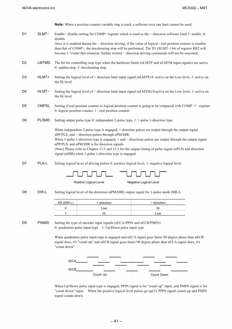
NOVA electronics Inc. MCX302 – M41
– 41 –
Note: When a position counter variable ring is used, a software over run limit cannot be used. D1 SLMT− Enable / disable setting for COMP− register which is used as the − direction software limit 1: enable, 0:
disable Once it is enabled during the − direction driving, if the value of logical / real position counter is smaller than that of COMP−, the decelerating stop will be performed. The D1 (SLMT−) bit of register RR2 will become 1. Under this situation, further written − direction driving commends will not be executed.
D2 LMTMD The bit for controlling stop type when the hardware limits (nLMTP and nLMTM input signals) are active
0: sudden stop, 1: decelerating stop D3 HLMT+ Setting the logical level of + direction limit input signal (nLMTP) 0: active on the Low level, 1: active on
the Hi level D4 HLMT− Setting the logical level of − direction limit input signal (nLMTM) 0:active on the Low level, 1: active on
the Hi level D5 CMPSL Setting if real position counter or logical position counter is going to be compared with COMP +/− register
0: logical position counter, 1 : real position counter D6 PLSMD Setting output pulse type 0: independent 2-pulse type, 1: 1-pulse 1-direction type
When independent 2-pulse type is engaged, + direction pulses are output through the output signal nPP/PLS, and − direction pulses through nPM/DIR. When 1-pulse 1-direction type is engaged, + and − directions pulses are output through the output signal nPP/PLS, and nPM/DIR is for direction signals. [Note] Please refer to Chapter 13.2 and 13.3 for the output timing of pulse signal (nPLS) and direction signal (nDIR) when 1-pulse 1-direction type is engaged.
D7 PLS-L Setting logical level of driving pulses 0: positive logical level, 1: negative logical level
Positive Logical Level
Negative Logical Level
D8 DIR-L Setting logical level of the direction (nPM/DIR) output signal for 1-pulse mode DIR-L
D8 (DIR-L) + direction − direction
0 Low Hi
1 Hi Low D9 PINMD Setting the type of encoder input signals (nECA/PPIN and nECB/PMIN)
0: quadrature pulse input type 1: Up/Down pulse input type
When quadrature pulse input type is engaged and nECA signal goes faster 90 degree phase than nECB signal does, it's "count up" and nECB signal goes faster 90 degree phase than nECA signal does, it's "count down"
When Up/Down pulse input type is engaged, PPIN signal is for “count up” input, and PMIN signal is for “count down” input. When the positive logical level pulses go up(↑), PPIN signal counts up and PMIN signal counts down.
Count Up Count Down
nECA
nECB
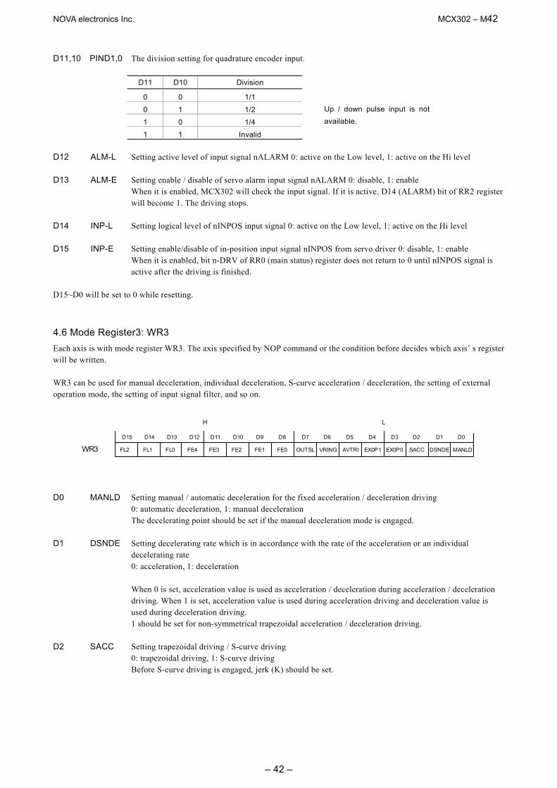
NOVA electronics Inc. MCX302 – M42
– 42 –
D11,10 PIND1,0 The division setting for quadrature encoder input.
D11 D10 Division
0 0 1/1
0 1 1/2
1 0 1/4
1 1 Invalid
Up / down pulse input is not available.
D12 ALM-L Setting active level of input signal nALARM 0: active on the Low level, 1: active on the Hi level D13 ALM-E Setting enable / disable of servo alarm input signal nALARM 0: disable, 1: enable
When it is enabled, MCX302 will check the input signal. If it is active, D14 (ALARM) bit of RR2 register will become 1. The driving stops.
D14 INP-L Setting logical level of nINPOS input signal 0: active on the Low level, 1: active on the Hi level
D15 INP-E Setting enable/disable of in-position input signal nINPOS from servo driver 0: disable, 1: enable
When it is enabled, bit n-DRV of RR0 (main status) register does not return to 0 until nINPOS signal is active after the driving is finished.
D15~D0 will be set to 0 while resetting.
4.6 Mode Register3: WR3 Each axis is with mode register WR3. The axis specified by NOP command or the condition before decides which axis’ s register will be written. WR3 can be used for manual deceleration, individual deceleration, S-curve acceleration / deceleration, the setting of external operation mode, the setting of input signal filter, and so on.
MANLD
H L
WR3
D12 D11
FL2
D15 D14 D13 D10 D9 D8 D7 D6 D5 D4 D3 D2 D1 D0
FL1 FL0 FE4 FE3 FE2 FE1 FE0 OUTSL VRING AVTRI EX0P1 EX0P0 SACC DSNDE
D0 MANLD Setting manual / automatic deceleration for the fixed acceleration / deceleration driving
0: automatic deceleration, 1: manual deceleration The decelerating point should be set if the manual deceleration mode is engaged.
D1 DSNDE Setting decelerating rate which is in accordance with the rate of the acceleration or an individual
decelerating rate 0: acceleration, 1: deceleration
When 0 is set, acceleration value is used as acceleration / deceleration during acceleration / deceleration driving. When 1 is set, acceleration value is used during acceleration driving and deceleration value is used during deceleration driving. 1 should be set for non-symmetrical trapezoidal acceleration / deceleration driving.
D2 SACC Setting trapezoidal driving / S-curve driving
0: trapezoidal driving, 1: S-curve driving Before S-curve driving is engaged, jerk (K) should be set.
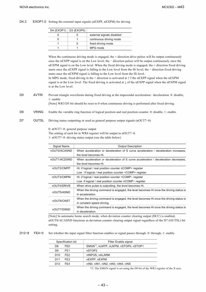
NOVA electronics Inc. MCX302 – M43
– 43 –
D4,3 EXOP1,0 Setting the external input signals (nEXPP, nEXPM) for driving
D4 (EXOP1) D3 (EXOP0)
0 0 external signals disabled 0 1 continuous driving mode 1 0 fixed driving mode 1 1 MPG mode
When the continuous driving mode is engaged, the + direction drive pulses will be output continuously once the nEXPP signal is on the Low level; the − direction pulses will be output continuously once the nEXPM signal is on the Low level. When the fixed driving mode is engaged, the + direction fixed driving starts once the nEXPP signal is falling to the Low level from the Hi level; the − direction fixed driving starts once the nEXPM signal is falling to the Low level from the Hi level. In MPG mode, fixed driving in the + direction is activated at ↑ f the nEXPP signal when the nEXPM signal is at the Low level. The fixed driving is activated at ↓ of the nEXPP signal when the nEXPM signal is at the Low level.
D5 AVTRI Prevent triangle waveforms during fixed driving at the trapezoidal acceleration / deceleration. 0: disable,
1: enable. [Note] WR3/D5 bit should be reset to 0 when continuous driving is performed after fixed driving. D6 VRING Enable the variable ring function of logical position and real position counter. 0: disable, 1: enable. D7 OUTSL Driving status outputting or used as general purpose output signals (nOUT7~0)
0: nOUT7~0: general purpose output The setting of each bit in WR4 register will be output to nOUT7~0. 1: nOUT7~0: driving status output (see the table below)
Signal Name Output Description
nOUT0/ACASND When acceleration or deceleration of S curve acceleration / deceleration increases,the level becomes Hi.
nOUT1/ACDSND When acceleration or deceleration of S curve acceleration / deceleration decreases,the level becomes Hi.
nOUT2/CMPP Hi: if logical / real position counter ≥COMP+ register Low : if logical / real position counter <COMP+ register
nOUT3/CMPM Hi: if logical / real position counter <COMP− register Low: if logical / real position counter ≥COMP− register
nOUT4/DRIVE When drive pulse is outputting, the level becomes Hi.
nOUT5/ASND When the driving command is engaged, the level becomes Hi once the driving status is in acceleration.
nOUT6/CNST When the driving command is engaged, the level becomes Hi once the driving status is in constant speed driving.
nOUT7/DSND When the driving command is engaged, the level becomes Hi once the driving status is in deceleration.
[Note] In automatic home search mode, when deviation counter clearing output (DCC) is enabled, nOUT0/ACASND functions as deviation counter clearing output signal regardless of the D7 (OUTSL) bit setting.
D12~8 FE4~0 Set whether the input signal filter function enables or signal passes through. 0: through, 1: enable.
Specification bit Filter Enable signal D8 FE0 EMGN*2, nLMTP, nLMTM, nSTOP0, nSTOP1 D9 FE1 nSTOP2 D10 FE2 nINPOS, nALARM D11 FE3 nEXPP, nEXPM D12 FE4 nIN0, nIN1, nIN2, nIN3, nIN4, nIN5
*2: The EMGN signal is set using the D8 bit of the WR3 register of the X axis.
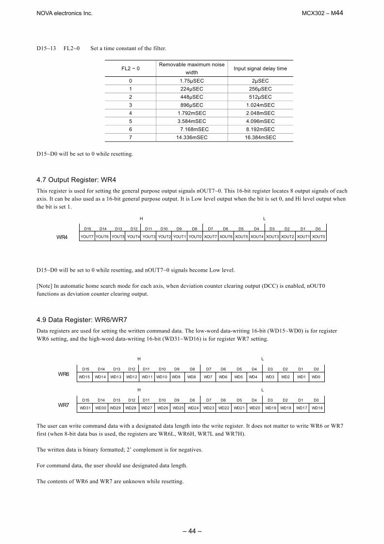
NOVA electronics Inc. MCX302 – M44
– 44 –
D15~13 FL2~0 Set a time constant of the filter.
FL2 ~ 0 Removable maximum noise
width Input signal delay time
0 1.75μSEC 2μSEC
1 224μSEC 256μSEC
2 448μSEC 512μSEC
3 896μSEC 1.024mSEC
4 1.792mSEC 2.048mSEC
5 3.584mSEC 4.096mSEC
6 7.168mSEC 8.192mSEC
7 14.336mSEC 16.384mSEC D15~D0 will be set to 0 while resetting.
4.7 Output Register: WR4 This register is used for setting the general purpose output signals nOUT7~0. This 16-bit register locates 8 output signals of each axis. It can be also used as a 16-bit general purpose output. It is Low level output when the bit is set 0, and Hi level output when the bit is set 1.
XOUT0 WR4
H L
YOUT7
D15 D14 D13 D12 D11 D10 D9 D8 D7 D6 D5 D4 D3 D2 D1 D0
YOUT6 YOUT5 YOUT4 YOUT3 YOUT2 YOUT1 YOUT0 XOUT7 XOUT6 XOUT5 XOUT4 XOUT3 XOUT2 XOUT1
D15~D0 will be set to 0 while resetting, and nOUT7~0 signals become Low level. [Note] In automatic home search mode for each axis, when deviation counter clearing output (DCC) is enabled, nOUT0 functions as deviation counter clearing output.
4.9 Data Register: WR6/WR7 Data registers are used for setting the written command data. The low-word data-writing 16-bit (WD15~WD0) is for register WR6 setting, and the high-word data-writing 16-bit (WD31~WD16) is for register WR7 setting.
WD16
WD0
WR6
H
L
WR7
H
L
WD15
D15
D14
D13
D12
D11
D10
D9
D8
D7
D6
D5
D4
D3
D2
D1
D0
WD14
WD13
WD12
WD11
WD10
WD9
WD8
WD7
WD6
WD5
WD4
WD3
WD2
WD1
WD31
D15
D14
D13
D12
D11
D10
D9
D8
D7
D6
D5
D4
D3
D2
D1
D0
WD30
WD29
WD28
WD27
WD26
WD25
WD24 WD23
WD22
WD21
WD20 WD19 WD18 WD17
The user can write command data with a designated data length into the write register. It does not matter to write WR6 or WR7 first (when 8-bit data bus is used, the registers are WR6L, WR6H, WR7L and WR7H). The written data is binary formatted; 2’ complement is for negatives. For command data, the user should use designated data length. The contents of WR6 and WR7 are unknown while resetting.
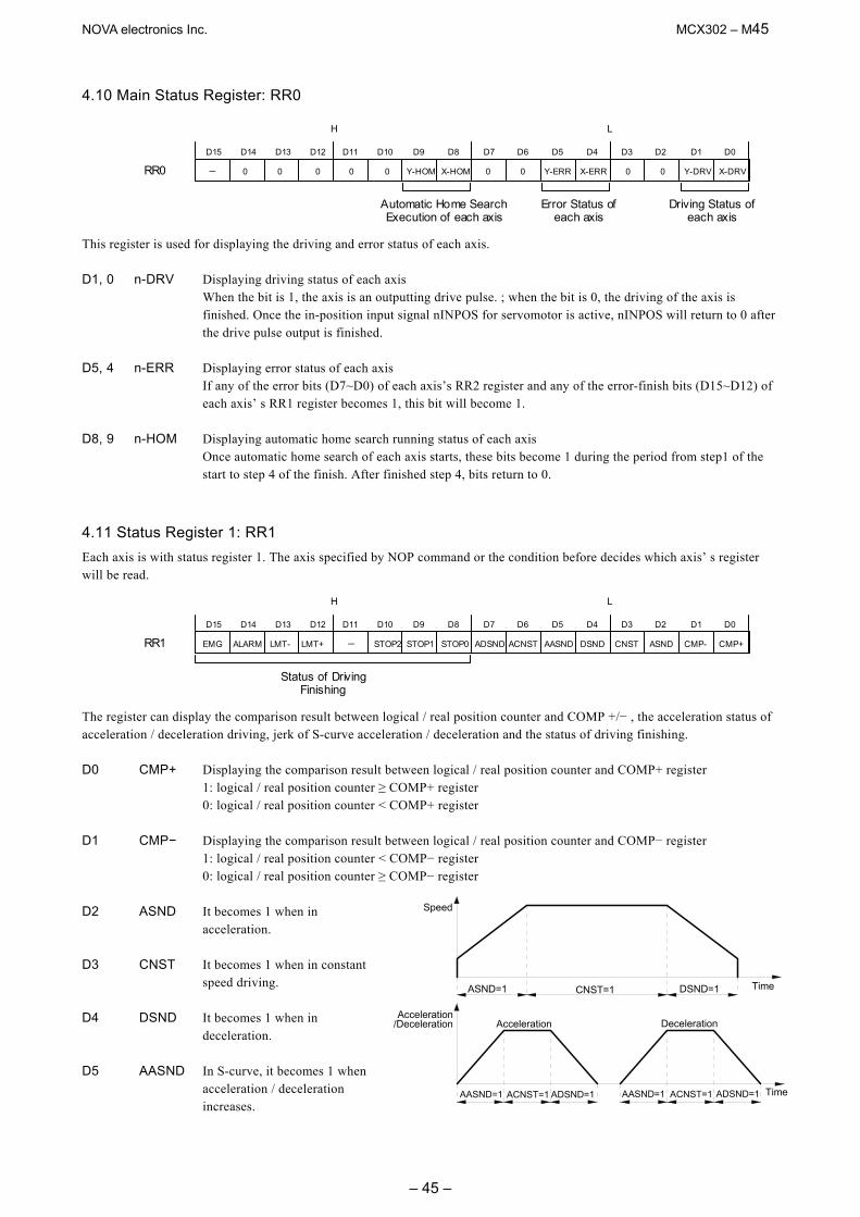
NOVA electronics Inc. MCX302 – M45
– 45 –
4.10 Main Status Register: RR0
H L
RR0
D15 D11 D12 D14 D13 D10 D9 D8 D7 D6 D5 D4 D3 D2 D1 D0
Y-HOM X-HOM Y-ERR X-ERR Y-DRV X-DRV - 0 0 0 0 0 0 0 0 0
Automatic Home Search Execution of each axis
Error Status of each axis
Driving Status of each axis
This register is used for displaying the driving and error status of each axis. D1, 0 n-DRV Displaying driving status of each axis
When the bit is 1, the axis is an outputting drive pulse. ; when the bit is 0, the driving of the axis is finished. Once the in-position input signal nINPOS for servomotor is active, nINPOS will return to 0 after the drive pulse output is finished.
D5, 4 n-ERR Displaying error status of each axis
If any of the error bits (D7~D0) of each axis’s RR2 register and any of the error-finish bits (D15~D12) of each axis’ s RR1 register becomes 1, this bit will become 1.
D8, 9 n-HOM Displaying automatic home search running status of each axis Once automatic home search of each axis starts, these bits become 1 during the period from step1 of the
start to step 4 of the finish. After finished step 4, bits return to 0.
4.11 Status Register 1: RR1 Each axis is with status register 1. The axis specified by NOP command or the condition before decides which axis’ s register will be read.
H L
RR1
Status of Driving Finishing
D15 D12 D11
EMG
D14 D13 D10 D9 D8 D7 D6 D5 D4 D3 D2 D1 D0
ALARM LMT- LMT+ - STOP2 STOP1 STOP0 ADSND ACNST AASND DSND CNST ASND CMP- CMP+
The register can display the comparison result between logical / real position counter and COMP +/− , the acceleration status of acceleration / deceleration driving, jerk of S-curve acceleration / deceleration and the status of driving finishing. D0 CMP+ Displaying the comparison result between logical / real position counter and COMP+ register 1: logical / real position counter ≥ COMP+ register 0: logical / real position counter < COMP+ register D1 CMP− Displaying the comparison result between logical / real position counter and COMP− register 1: logical / real position counter < COMP− register 0: logical / real position counter ≥ COMP− register D2 ASND It becomes 1 when in
acceleration. D3 CNST It becomes 1 when in constant
speed driving. D4 DSND It becomes 1 when in
deceleration. D5 AASND In S-curve, it becomes 1 when
acceleration / deceleration increases.
ASND=1 CNST=1 DSND=1
Speed
Time
Acceleration/Deceleration Acceleration Deceleration
AASND=1 ACNST=1 AASND=1 ACNST=1 ADSND=1 TimeADSND=1
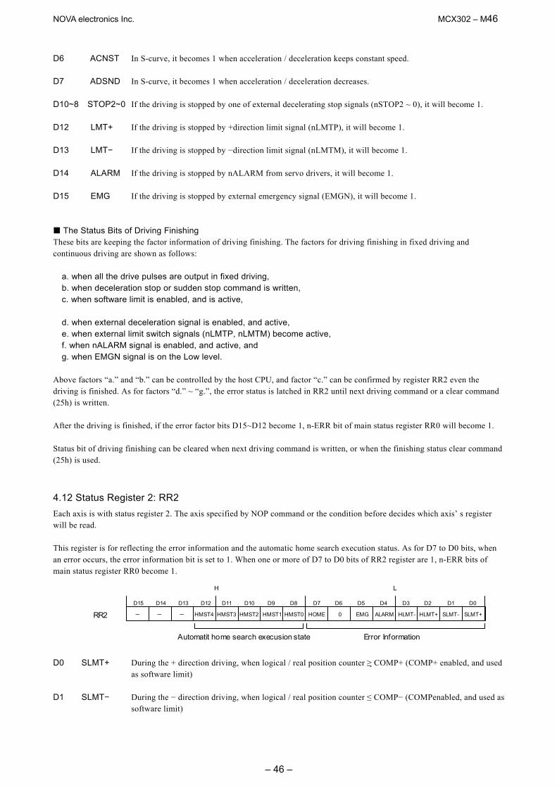
NOVA electronics Inc. MCX302 – M46
– 46 –
D6 ACNST In S-curve, it becomes 1 when acceleration / deceleration keeps constant speed. D7 ADSND In S-curve, it becomes 1 when acceleration / deceleration decreases. D10~8 STOP2~0 If the driving is stopped by one of external decelerating stop signals (nSTOP2 ~ 0), it will become 1. D12 LMT+ If the driving is stopped by +direction limit signal (nLMTP), it will become 1. D13 LMT− If the driving is stopped by −direction limit signal (nLMTM), it will become 1. D14 ALARM If the driving is stopped by nALARM from servo drivers, it will become 1. D15 EMG If the driving is stopped by external emergency signal (EMGN), it will become 1.
The Status Bits of Driving Finishing These bits are keeping the factor information of driving finishing. The factors for driving finishing in fixed driving and continuous driving are shown as follows: a. when all the drive pulses are output in fixed driving, b. when deceleration stop or sudden stop command is written, c. when software limit is enabled, and is active, d. when external deceleration signal is enabled, and active, e. when external limit switch signals (nLMTP, nLMTM) become active, f. when nALARM signal is enabled, and active, and g. when EMGN signal is on the Low level. Above factors “a.” and “b.” can be controlled by the host CPU, and factor “c.” can be confirmed by register RR2 even the driving is finished. As for factors “d.” ~ “g.”, the error status is latched in RR2 until next driving command or a clear command (25h) is written. After the driving is finished, if the error factor bits D15~D12 become 1, n-ERR bit of main status register RR0 will become 1. Status bit of driving finishing can be cleared when next driving command is written, or when the finishing status clear command (25h) is used.
4.12 Status Register 2: RR2 Each axis is with status register 2. The axis specified by NOP command or the condition before decides which axis’ s register will be read. This register is for reflecting the error information and the automatic home search execution status. As for D7 to D0 bits, when an error occurs, the error information bit is set to 1. When one or more of D7 to D0 bits of RR2 register are 1, n-ERR bits of main status register RR0 become 1.
H L
RR2
Automatit home search execusion state Error Information
-
D15 D14 D13 D12 D11 D10 D9 D8 D7 D6 D5 D4 D3 D2 D1 D0
HOME - - HMST4 HMST3 HMST2 HMST1 HMST0 0 EMG ALARM HLMT- HLMT+ SLMT- SLMT+
D0 SLMT+ During the + direction driving, when logical / real position counter ≥ COMP+ (COMP+ enabled, and used
as software limit) D1 SLMT− During the − direction driving, when logical / real position counter ≤ COMP− (COMPenabled, and used as
software limit)
NOVA electronics Inc. MCX302 – M47
– 47 –
D2 HLMT+ When external +direction limit signal (nLMTP) is on its active level D3 HLMT− When external −direction limit signal (nLMTM) is on its active level D4 ALARM When the alarm signal (nALARM) for servo motor is on its active level D5 EMG When emergency stop signal (EMGN) becomes Low level. D7 HOME Error during automatic home search execution
When encoder z-phase signal (nSTOP2) is already active at the start of step 3, it will become 1. D12~8 HMST4~0 Autoamtic home search execution state displays the current executing action during automatic home
search execution. Please refer to 2.4.4. In driving, when hardware / software limit is active, the decelerating stop or sudden stop will be executed. Bit SLMT+ / − will not become 1 during the reverse direction driving.
4.13 Status Register 3: RR3 Each axis is with status register 3. The axis specified by NOP command or the condition before decides which axis’ s register will be read. This register is for reflecting the interrupt factor. When interrupt happens, the bit with the interrupt factor becomes 1. The user should set the interrupt factor through register WR1 to perform the interrupt.
H L
RR3 -
D15 D14 D13 D12 D11 D10 D9 D8 D7 D6 D5 D4 D3 D2 D1 D0
D-END - - C-STA P<C+ P<C- - - - - - C-END P≧C+ - P≧C-
To generate an interrupt, interrupt enable must be set for each factor in the WR1 register. D1 P ≥ C− Once the value of logical / real position counter is larger than that of COMP− register D2 P < C− Once the value of logical / real position counter is smaller than that of COMP− register D3 P < C+ Once the value of logical / real position counter is smaller than that of COMP+ register D4 P ≥ C+ Once the value of logical / real position counter is larger than that of COMP+ register D5 C-END When the pulse output is finished in the constant speed drive during an acceleration / deceleration driving D6 C-STA When the pulse output is started in the constant speed drive during an acceleration / deceleration driving D7 D-END When the driving is finished When one of the interrupt factors occurs an interrupt, the bit of the register becomes 1, and the interrupt output signal (INTN) will become the Low level. The host CPU will read register RR3 of the interrupted axis, the bit of RR3 will be cleared to 0, and the interrupt signal will return to the non-active level. For a 8-bit data bus, all the bits are cleared when the RR3L register is read.
NOVA electronics Inc. MCX302 – M48
– 48 –
4.14 Input Register: RR4 / RR5 RR4 and RR5 are used for displaying the input signal status. The bit is 0 if the input is on the Low level; the bit is 1 if the input is on the Hi level. These input signals can be used as general input signal when they are not used as function except for nLMTP/M signal.
Y-ST0
X-ST0
RR4
H
L
RR5
H
L
X-LM-
D15
D14
D13
D12
D11
D10
D9
D8
D7
D6
D5
D4
D3
D2
D1
D0
X-LM+
X-IN5
X-IN4
X-IN3
X-IN2
X-IN1
X-IN0
X-ALM
X-INP
X-EX-
X-EX+
EMG X-ST2
X-ST1
Y-LM-
D15
D14
D13
D12
D11
D10
D9
D8
D7
D6
D5
D4
D3
D2
D1
D0
Y-LM+
Y-IN5
Y-IN4
Y-IN3
Y-IN2
Y-IN1
Y-IN0 Y-ALM
Y-INP
Y-EX-
Y-EX+ - Y-ST2 Y-ST1
Bit Name Input Signal Bit Name Input Signal
n-ST0 n-ST1 n-ST2 EMG
n-EX+ n-EX- n-INP n-ALM
n-STOP0 n-STOP1 n-STOP2
EMGN nEXPP nEXPM nINPOS nALARM
n-IN0 n-IN1 n-IN2 n-IN3 n-IN4 n-IN5 n-LM+ n-LM-
nIN0 nIN1 nIN2 nIN3 nIN4 nIN5
nLMTP nLMTM
4.15 Data-Read Register: RR6 / RR7 According to the data-read command, the data of internal registers will be set into registers RR6 and RR7. The low word 16 bits (D15 ~ D0) is set in RR6 register, and the high word 16 bits (D31 ~ D16) is set in RR7 register for data reading.
RD16
RD0
RR6
H
L
RR7
H
L
RD15
D15
D14
D13
D12
D11
D10
D9
D8
D7
D6
D5
D4
D3
D2
D1
D0
RD14
RD13
RD12
RD11
RD10
RD9
RD8
RD7
RD6
RD5
RD4
RD3 RD2
RD1
RD31
D15
D14
D13
D12
D11
D10
D9
D8
D7
D6
D5
D4
D3
D2
D1
D0
RD30
RD29
RD28
RD27 RD26
RD25
RD24 RD23 RD22
RD21
RD20 RD18 RD17
RD19
The data is binary formatted; 2’ s complement is for negatives.
NOVA electronics Inc. MCX302 – M49
– 49 –
5. Command Lists
Write Commands
Code Command Symbol Data Range Data Length
00h Range setting R R 8,000,000(multiple=1) ~ 16,000(multiple=500) 4 bytes
01 Jerk setting (Acceleration increasing rate)
K 1 ~ 65,535 2
02 Acceleration setting A 1 ~ 8,000 2 03 Deceleration setting D 1 ~ 8,000 2 04 Initial speed setting SV 1 ~ 8,000 2 05 Drive speed setting V 1 ~ 8,000 2 06 Output pulse numbers P 0 ~ 268,435,455 4 07 Manual deceleration point setting DP 0 ~ 268,435,455 4 09 Logical position counter setting LP −2,147,483,648 ~ +2,147,483,647 4 0A Real position counter setting EP −2,147,483,648 ~ +2,147,483,647 4 0B COMP + register setting CP −1,073,741,824 ~ +1,073,741,824 4 0C COMP − register setting CM −1,073,741,824 ~ +1,073,741,824 4 0D Acceleration counter offsetting AO −32,768 ~ +32,767 2
0F NOP (For axis switching) 60 Automatic home search mode setting HM 2 61 Home search speed setting HV 1 ~ 8,000 2
[Note] When those parameters are written, the total data length should be completely filled. [Formula Calculation for Parameters]
Multiple = R
8,000,000
Jerk (PPS/SEC ) = K
62.5 ×10
2
6
×
R
8,000,000
Multiple
Acceleration (PPS/SEC) = R
8,000,000
Multiple
A ×125 ×
Drive Speed (PPS) = R
8,000,000
Multiple
V ×
Deceleration (PPS/SEC) = R
8,000,000
Multiple
D ×125 ×
Init ial Speed (PPS) = R
8,000,000
Multiple
SV×
NOVA electronics Inc. MCX302 – M50
– 50 –
Data Reading Commands
Code Command Symbol Data Range Data Length10h Logical position counter reading LP −2,147,483,648 ~ +2,147,483,647 4 bytes 11 Real position counter reading EP −2,147,483,648 ~ +2,147,483,647 4 12 Current drive speed reading CV 1 ~ 8,000 2 13 Acceleration / deceleration reading CA 1 ~ 8,000 2
Driving Commands
Code Command 20h + direction fixed driving 21 − direction fixed driving 22 + direction continuous driving 23 − direction continuous driving 24 Drive start holding
25 Drive start holding release / stop status clear
26 Decelerating stop 27 Sudden stop
Other Commands
Code Command 62h Automatic home search execution63 Deviation counter clearing output
[Note] Please do not write the codes not mentioned above. The unknown situation could happen due to IC internal circuit test.
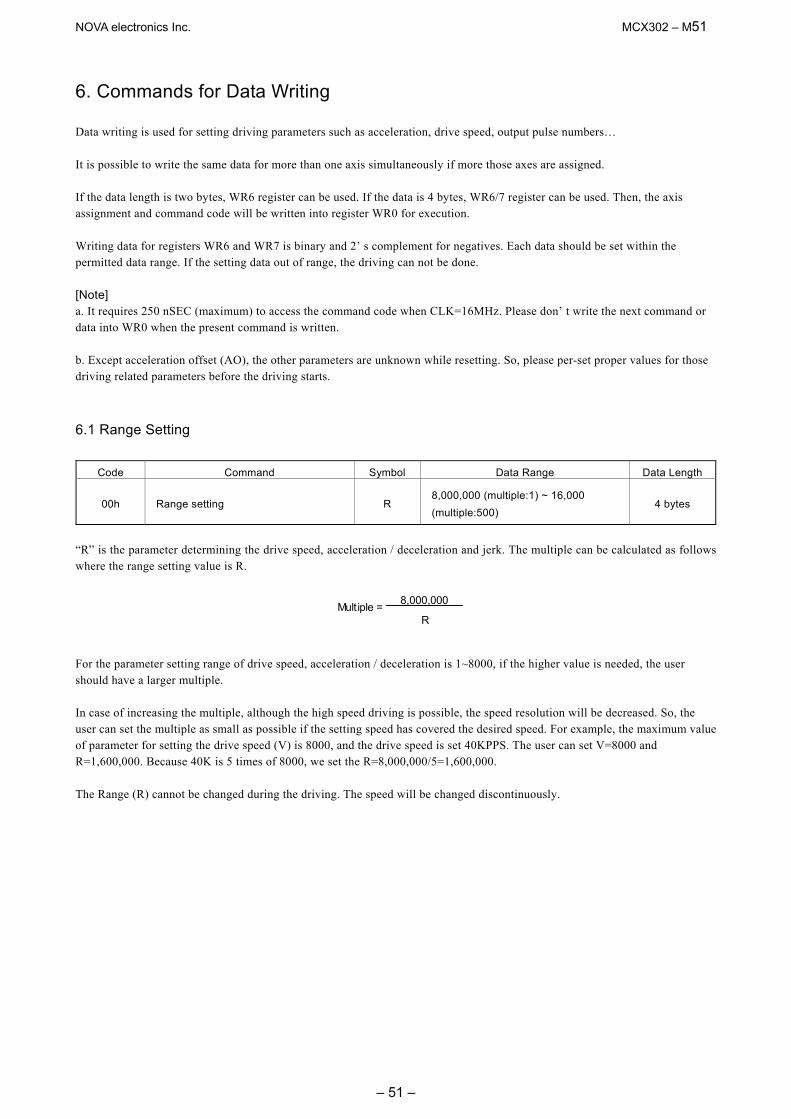
NOVA electronics Inc. MCX302 – M51
– 51 –
6. Commands for Data Writing Data writing is used for setting driving parameters such as acceleration, drive speed, output pulse numbers… It is possible to write the same data for more than one axis simultaneously if more those axes are assigned. If the data length is two bytes, WR6 register can be used. If the data is 4 bytes, WR6/7 register can be used. Then, the axis assignment and command code will be written into register WR0 for execution. Writing data for registers WR6 and WR7 is binary and 2’ s complement for negatives. Each data should be set within the permitted data range. If the setting data out of range, the driving can not be done. [Note] a. It requires 250 nSEC (maximum) to access the command code when CLK=16MHz. Please don’ t write the next command or data into WR0 when the present command is written. b. Except acceleration offset (AO), the other parameters are unknown while resetting. So, please per-set proper values for those driving related parameters before the driving starts.
6.1 Range Setting
Code Command Symbol Data Range Data Length
00h Range setting R 8,000,000 (multiple:1) ~ 16,000 (multiple:500)
4 bytes
“R” is the parameter determining the drive speed, acceleration / deceleration and jerk. The multiple can be calculated as follows where the range setting value is R.
Multiple = R
8,000,000
For the parameter setting range of drive speed, acceleration / deceleration is 1~8000, if the higher value is needed, the user should have a larger multiple. In case of increasing the multiple, although the high speed driving is possible, the speed resolution will be decreased. So, the user can set the multiple as small as possible if the setting speed has covered the desired speed. For example, the maximum value of parameter for setting the drive speed (V) is 8000, and the drive speed is set 40KPPS. The user can set V=8000 and R=1,600,000. Because 40K is 5 times of 8000, we set the R=8,000,000/5=1,600,000. The Range (R) cannot be changed during the driving. The speed will be changed discontinuously.
NOVA electronics Inc. MCX302 – M52
– 52 –
6.2 Jerk Setting
Code Command Symbol Data Range Data Length
01h Jerk setting K 1 ~ 65,535 2 bytes
A jerk setting value is a parameter that determines the acceleration increase/decrease rate per unit in S-curve acceleration/deceleration. “K” is the parameter determining the jerk. The jerk calculation is shown in the following formula:
Jerk (PPS/SEC ) =
K
62.5 ×10
2
6
×
R
8,000,000
Multiple
Because the setting range of jerk is 1 ~ 65,535, the jerk range is shown as follows: When Multiple = 1, 954 PPS/SEC2 ~ 62.5 × 10⁶ PPS/SEC2 When Multiple = 500, 477 × 103 PPS/SEC2 ~ 31.25 109 PPS/SEC2 [Note] This book uses the word “jerk” to express increase / decrease of acceleration / deceleration and increase / decrease rate per unit.
6.3 Acceleration Setting
Code Command Symbol Data Range Data Length
02h Acceleration setting A 1 ~ 8,000 2 bytes
In linear acceleration / deceleration driving, “A” is the parameter determining the acceleration at acceleration and deceleration at deceleration. Acceleration / deceleration increases on a straight line from 0 to the specified value when S-curve acceleration / deceleration driving. Please refer to Fig. 2.13 The acceleration calculation is shown in the following formula:
Acceleration (PPS/SEC) = R
8,000,000
Multiple
A ×125 ×
For the range of A is from 1 ~ 8,000, the actual acceleration range is shown as follows: When Multiple = 1, 125 PPS/SEC ~ 1 × 10⁶ PPS/SEC When Multiple = 500, 62.5 × 10³ PPS/SEC ~ 500 × 106 PPS/SEC
NOVA electronics Inc. MCX302 – M53
– 53 –
6.4 Deceleration Setting
Code Command Symbol Data Range Data Length
03h Deceleration setting D 1 ~ 8,000 2 bytes
In linear acceleration / deceleration driving, “D” is the parameter determining the deceleration at deceleration in the acceleration / deceleration individual settings mode (WR3register D1=1). Deceleration increases on a straight line from 0 to the specified value when S-curve acceleration / deceleration driving in this mode. The deceleration calculation is shown in the following formula:
Deceleration (PPS/SEC) = R
8,000,000
Multiple
D ×125 ×
6.5 Initial Speed Setting
Code Command Symbol Data Range Data Length
04h Initial speed setting SV 1 ~ 8,000 2 bytes
“SV” is the parameter determining the speed of initial speed. The initial speed calculation is shown in the following formula:
Init ial Speed (PPS) = R
8,000,000
Multiple
SV×
In trapezoidal(Linear) accerelation/decerelation driving, for stepper motors, the user should set the initial speed smaller than the self-starting frequency of stepper motors. Also for a servo motor, if the value that is set is too low, creep or premature termination may occur. In this case, it is appropriate to set the value larger than √(acceleration). For instance, when acceleration=125000 PPS/SEC, the value should be larger than √(125000)=354 PPS. In fixed pulse S curve acceleration / deceleration driving, if the value that is set is too low such as SV is set less than 100, creep or premature termination may occur as well. Set the intial speed value (SV) as more than 100.
6.6 Drive Speed Setting
Code Command Symbol Data Range Data Length
05h Drive speed setting V 1 ~ 8,000 2 bytes
“V” is the parameter determining the speed of constant speed period in trapezoidal driving. In constant speed driving, the drive speed is the initial speed. The drive speed calculation is shown in the following formula:
Drive Speed (PPS) = R
8,000,000
Multiple
V ×
If the setting drive speed is lower than the initial speed, the acceleration / deceleration will not be performed, and the driving is
NOVA electronics Inc. MCX302 – M54
– 54 –
constant speed. During the encoder Z-phase searching (at a low-peed driving), if the user want to perform the sudden stop once the Z-phase is detected, the drive speed should be set lower than the initial speed. Drive speed can be altered during the driving. When the drive speed of next constant speed period is set, the acceleration / deceleration will be performed to reach the new setting drive speed, then a constant speed driving starts.
In automatic home search, this drive speed is used for high-speed search speed of Step1 and the high-speed drive speed of Step4.
[Note] a. In fixed S-curve acceleration / deceleration driving, there is no way to change the drive speed during the driving. In
continuous S-curve acceleration / deceleration driving, the S-curve profile cannot be exactly tracked if the speed alterations during the acceleration / deceleration. it is better to change the drive speed in the constant speed period.
b. In fixed trapezoidal driving, the frequent changes of drive speed may occur residual pulses at the end of deceleration.
6.7 Output Pulse Number
Code Command Symbol Data Range Data Length
06h Output pulse number P 0 ~ 268,435,455 4 bytes
The number of output pulses indicates the total number of pulses that are output in fixed driving. Set with an unsigned 4 bytes data length. The output pulse numbers can be changed during the driving. In automatic home search, this number of output pulses is used for the offset drive pulses at Step 4.
6.8 Manual Decelerating Point Setting
Code Command Symbol Data Range Data Length
07h Manual decelerating point setting DP 0 ~ 268,435,455 4 bytes
“DP” is the parameter setting the manual deceleration point in fixed acceleration / deceleration driving when the manual deceleration mode is engaged. In manual deceleration mode, the user can set the bit D0 of WR3 register to 1. The decelerating point can be set:
Manual Decelerating Point = Output Pulse Number − Pulse Number for Deceleration
6.9 Logical Position Counter Setting
Code Command Symbol Data Range Data Length
09h Logical position counter setting LP −2,147,483,648 ~ +2,147,483,647 4 bytes
“LP” is the parameter setting the value of logic position counter. Logical position counter counts Up / Down according to the +/− direction pulse output. The data writing and reading of logical position counter is possible anytime.
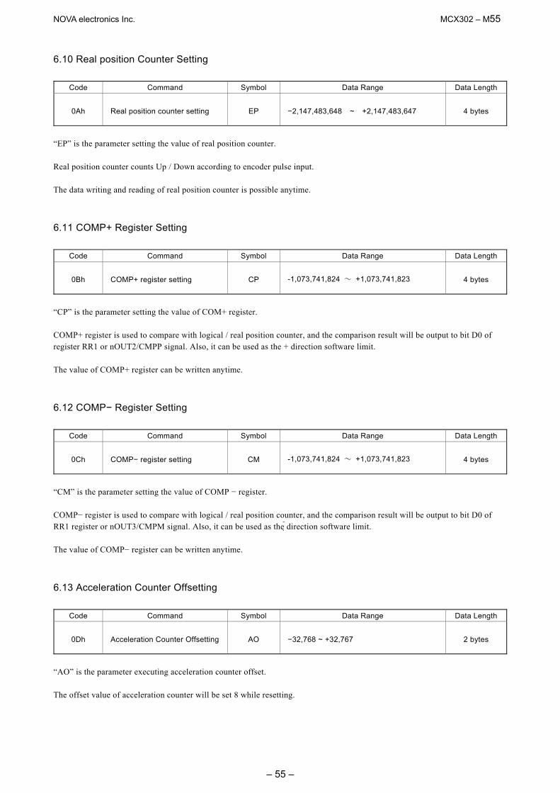
NOVA electronics Inc. MCX302 – M55
– 55 –
6.10 Real position Counter Setting
Code Command Symbol Data Range Data Length
0Ah Real position counter setting EP −2,147,483,648 ~ +2,147,483,647 4 bytes
“EP” is the parameter setting the value of real position counter. Real position counter counts Up / Down according to encoder pulse input. The data writing and reading of real position counter is possible anytime.
6.11 COMP+ Register Setting
Code Command Symbol Data Range Data Length
0Bh COMP+ register setting CP -1,073,741,824 ~ +1,073,741,823 4 bytes
“CP” is the parameter setting the value of COM+ register. COMP+ register is used to compare with logical / real position counter, and the comparison result will be output to bit D0 of register RR1 or nOUT2/CMPP signal. Also, it can be used as the + direction software limit. The value of COMP+ register can be written anytime.
6.12 COMP− Register Setting
Code Command Symbol Data Range Data Length
0Ch COMP− register setting CM -1,073,741,824 ~ +1,073,741,823 4 bytes
“CM” is the parameter setting the value of COMP − register. COMP− register is used to compare with logical / real position counter, and the comparison result will be output to bit D0 of RR1 register or nOUT3/CMPM signal. Also, it can be used as the direction software limit. The value of COMP− register can be written anytime.
6.13 Acceleration Counter Offsetting
Code Command Symbol Data Range Data Length
0Dh Acceleration Counter Offsetting AO −32,768 ~ +32,767 2 bytes
“AO” is the parameter executing acceleration counter offset. The offset value of acceleration counter will be set 8 while resetting.
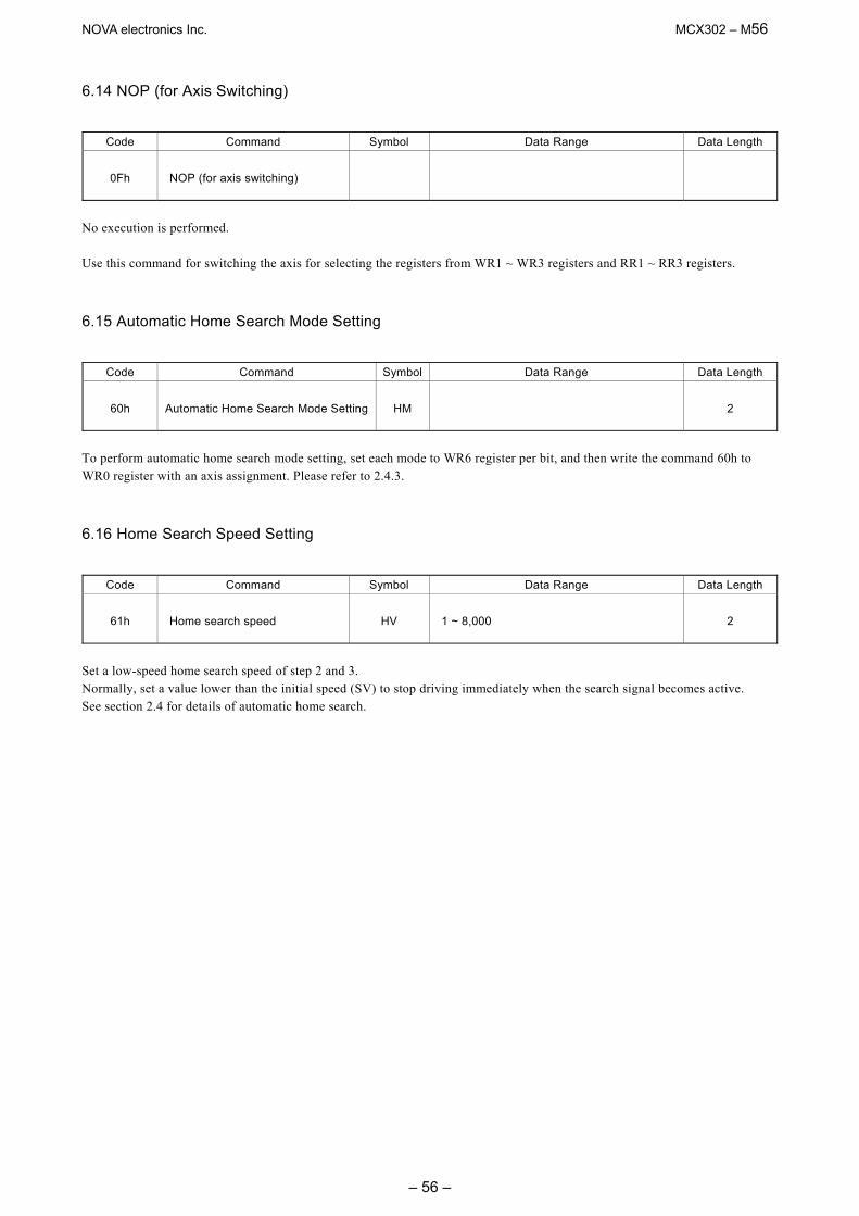
NOVA electronics Inc. MCX302 – M56
– 56 –
6.14 NOP (for Axis Switching)
Code Command Symbol Data Range Data Length
0Fh NOP (for axis switching)
No execution is performed. Use this command for switching the axis for selecting the registers from WR1 ~ WR3 registers and RR1 ~ RR3 registers.
6.15 Automatic Home Search Mode Setting
Code Command Symbol Data Range Data Length
60h Automatic Home Search Mode Setting HM 2
To perform automatic home search mode setting, set each mode to WR6 register per bit, and then write the command 60h to WR0 register with an axis assignment. Please refer to 2.4.3.
6.16 Home Search Speed Setting
Code Command Symbol Data Range Data Length
61h Home search speed HV 1 ~ 8,000 2
Set a low-speed home search speed of step 2 and 3. Normally, set a value lower than the initial speed (SV) to stop driving immediately when the search signal becomes active. See section 2.4 for details of automatic home search.
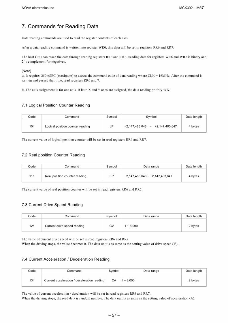
NOVA electronics Inc. MCX302 – M57
– 57 –
7. Commands for Reading Data Data reading commands are used to read the register contents of each axis. After a data reading command is written into register WR0, this data will be set in registers RR6 and RR7. The host CPU can reach the data through reading registers RR6 and RR7. Reading data for registers WR6 and WR7 is binary and 2’ s complement for negatives. [Note] a. It requires 250 nSEC (maximum) to access the command code of data reading where CLK = 16MHz. After the command is written and passed that time, read registers RR6 and 7. b. The axis assignment is for one axis. If both X and Y axes are assigned, the data reading priority is X.
7.1 Logical Position Counter Reading
Code Command Symbol Symbol Data length
10h Logical position counter reading LP −2,147,483,648 ~ +2,147,483,647 4 bytes
The current value of logical position counter will be set in read registers RR6 and RR7.
7.2 Real position Counter Reading
Code Command Symbol Data range Data length
11h Real position counter reading EP −2,147,483,648 ~ +2,147,483,647 4 bytes
The current value of real position counter will be set in read registers RR6 and RR7.
7.3 Current Drive Speed Reading
Code Command Symbol Data range Data length
12h Current drive speed reading CV 1 ~ 8,000 2 bytes
The value of current drive speed will be set in read registers RR6 and RR7. When the driving stops, the value becomes 0. The data unit is as same as the setting value of drive speed (V).
7.4 Current Acceleration / Deceleration Reading
Code Command Symbol Data range Data length
13h Current acceleration / deceleration reading CA 1 ~ 8,000 2 bytes
The value of current acceleration / deceleration will be set in read registers RR6 and RR7. When the driving stops, the read data is random number. The data unit is as same as the setting value of acceleration (A).
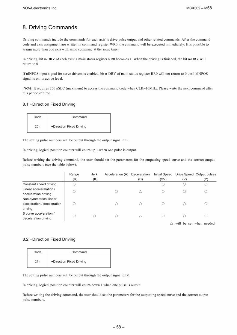
NOVA electronics Inc. MCX302 – M58
– 58 –
8. Driving Commands Driving commands include the commands for each axis’ s drive pulse output and other related commands. After the command code and axis assignment are written in command register WR0, the command will be executed immediately. It is possible to assign more than one axis with same command at the same time. In driving, bit n-DRV of each axis’ s main status register RR0 becomes 1. When the driving is finished, the bit n-DRV will return to 0. If nINPOS input signal for servo drivers is enabled, bit n-DRV of main status register RR0 will not return to 0 until nINPOS signal is on its active level. [Note] It requires 250 nSEC (maximum) to access the command code when CLK=16MHz. Please write the next command after this period of time.
8.1 +Direction Fixed Driving
Code Command
20h +Direction Fixed Driving
The setting pulse numbers will be output through the output signal nPP. In driving, logical position counter will count-up 1 when one pulse is output. Before writing the driving command, the user should set the parameters for the outputting speed curve and the correct output pulse numbers (see the table below). Range
(R) Jerk (K)
Acceleration (A) Deceleration (D)
Initial Speed (SV)
Drive Speed (V)
Output pulses (P)
Constant speed driving Linear acceleralation / decelaration driving
Non-symmetrical linear acceleration / deceleration driving
S curve acceleration / deceleration driving
will be set when needed
8.2 −Direction Fixed Driving
Code Command
21h −Direction Fixed Driving
The setting pulse numbers will be output through the output signal nPM. In driving, logical position counter will count-down 1 when one pulse is output. Before writing the driving command, the user should set the parameters for the outputting speed curve and the correct output pulse numbers.
NOVA electronics Inc. MCX302 – M59
– 59 –
8.3 +Direction Continuous Driving
Code Command
22h +Direction Continuous Driving
Before the stop command or external signal is active, the pulse numbers will be continuously output through the output signal nPP. In driving, logical position counter will count-up 1 when one pulse is output. Before writing the driving command, the user should set the parameters for the outputting speed curve and the correct output pulse numbers.
8.4 −Direction Continuous Driving
Code Command
23h −Direction Continuous Driving
Before the stop command or external signal is active, the pulse numbers will be continuously output through the output signal nPM. In driving, logical position counter will count-down 1 when one pulse is output. Before writing the driving command, the user should set the parameters for the outputting speed curve and the correct output pulse numbers.
8.5 Drive Status Holding
Code Command
24h Holding for driving starting
This command is to hold-on the start of driving. When this command is used for starting multi-axis driving simultaneously, the user may write other commands after the drive status holding command is registered. The drive start holding release command (25h) can be written to start the driving. In driving, even this command is written, the driving will not be stopped. The next command will be held.
8.6 Drive Status Holding Release / Finishing Status Clear
Code Command
25h Drive status holding release / finishing status clearing
This command is to release the drive status holding (24h), and start the driving. Also, this command can clear the finishing status bits D15 ~ 8 of register RR1 and the automatic home search STOP2 signal error bit D7 (HOME) of register RR2.
NOVA electronics Inc. MCX302 – M60
– 60 –
8.7 Decelerating Stop
Code Command
26h Decelerating stop in driving
This command performs the decelerating stop when the drive pulses are outputting. If the drive speed is lower than the initial speed, the driving will be suddenly stopped when this command is engaged. Once the driving stops, this command will not work.
8.8 Sudden Stop
Code Command
27h Sudden stop in driving
This command performs the sudden stop when the drive pulses are output. Also, the sudden stop can be performed in acceleration / deceleration driving. Once the driving stops, this command will not work.
NOVA electronics Inc. MCX302 – M61
– 61 –
9. Other Commands [Note] It requires 250 nSEC (maximum) to access the command code when CLK=16MHz. Please write the next command after this period of time.
9.1 Automatic Home Search Execution
Code Command
62h Automatic home search execution
This command executes automatic home search. Before execution of command, the automatic home search mode and correct parameters must be set. See section 2.4 for details of automatic home search.
9.2 Deviation Counter Clear Output
Code Command
63h Deviation counter clear output
This command outputs deviation counter clear pulses from the nOUT0/ACASND/DCC outoput pin. Before issuing this command, set output enable, a pulse logical level, and a pulse width in using the exetension mode setting command. See section 2.4.2 for details.
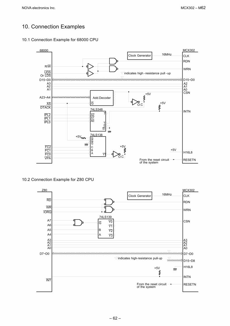
NOVA electronics Inc. MCX302 – M62
– 62 –
10. Connection Examples
10.1 Connection Example for 68000 CPU
10.2 Connection Example for Z80 CPU
MCX302
G
Clock Generator 16MHz
indicates high - resistance pull -up
Add.Decoder
O.C
+5V
7
10
EI
A0A1A2
ABCGGG
Y7
74LS138
74LS348
+5V
+5V
+5V
O.C
+5V
68000
A3A2A1
A23~A4
AS
R/W
Or LDSD15~D0
DTACK
IPL2IPL1IPL0
FC2FC1FC0VPA
UDS
A2A1A0
D15~D0
CLK
RDN
WRN
CSN
H16L8
RESETN
INTN
From the reset circuitof the system
Clock Generator 16MHz
indicates high- resistance pull-up
+5V
Z80
RD
WRIORQ
D7~D0
INT
A7A6A5A4
A3A2A1A0
74LS139
G
A
Y0
Y2Y3
BY1
MCX302
A2A1
CLK
RDN
WRN
CSN
H16L8
RESETN
INTN
A3
A0
D7~D0
D15~D8
From the reset circuitof the system
NOVA electronics Inc. MCX302 – M63
– 63 –
10.3 Example of Connection with H8 CPU
Example of 8 -bit Bus Mode Connection
H8/3048
A3A2A1
D15~D0
RD
HWR
CS4
IRQ4
XTAL
EXTAL 16MHz
indicates high- resistance pull-up+5V
+5V
Crystal/CeramicOscillator
Address Assignment in Mode 5
Low -order data (D15~D0)
16MHz
High -order data (D31~D16)
MCX302
A2A1A0
D15~D0
CLK
RDN
WRN
CSN
H16L8
RESETN
INTN
H8/3048
A3A2A1
D15~D8
RD
HWR
CS4
IRQ4
XTAL
EXTAL
A0
16MHz
+5V
MCX302
A2A1A0
D7~D0
CLK
RDN
WRN
CSN
H16L8
RESETN
INTN
A3
D15~D8
Example of 16 -bit Bus Mode Connection
indicates high- resistance pull-up
From the reset circuitof the system
Address Write Register Read Register80000800028000480006800088000A8000C8000E
WR0WR1WR2WR3WR4
WR6WR7
RR0RR1RR2RR3RR4RR5RR6RR7
From the reset circuitof the system
NOVA electronics Inc. MCX302 – M64
– 64 –
10.4 Connection Example The figure shown below illustrates the example of X axis driving system. Y axis can be assigned in the same way.
10.5 Pulse Output Interface
Output to Motor Drivers in Differential Circuit
Open Collector TTL Output
For drive pulse output signals, we recommend the user to use twist pair shield cable due to the concern of EMC.
EC
Stepper/ServoEncoder
M- Limit Near HomeHome + Limit
MCX302
1/2Motor Drives
I/F
I/F
I/FXPPXPM
XOUT0XOUT1
CW PulseCCW Pulse
Error Counter ClearServo ON/OFF
AlarmPositioning Conpletion
Servo Ready
EC -A/B,Z
XIN0XINPOS
XALARMXECA/B,XSTOP2
EC -A,B,Z
XLMTPXLMTM
XSTOP0XSTOP1
XEXPPXEXPM I/F
Manual Operation
+
-
+
-
GNDTwist Pair Shield Cable
Motor Drives
Am26LS32Am26LS31
XPP
XPM
CW+
CW -
CCW+
CCW -
GND
MCX302
CW+
CW -
CCW+
CCW -
Twist Pair Shield Cable
GND
+5V
+5V
74LS06
MCX302
XPP
XPM
Motor Drives
NOVA electronics Inc. MCX302 – M65
– 65 –
10.6 Connection Example for Input Signals Limit signals often pick up some noise since complicated cabling is normally involved. A photo coupler alone may not be able to absorb this noise. Enable the filter function in the IC and set an appropriate time constant (FL=2,3).
10.7 Connection Example for Encoder The following diagram is the example for the encoder signal which is differential line-drive output. Then, this signal can be received through the high speed photo coupler IC which can direct it to MCX302.
+5V
10K 3.3K
+12~24V
TLP121X Axis + Over Run Limit
XLMTPIntegralFilterEnable
Disable
To the internalcircuit
MCX302
MCX302
220
1K470
+5V
TLP115A
ECA+
ECA -XECA
Motor Drives
NOVA electronics Inc. MCX302 – M66
– 66 –
11. Example Program The example of C program for MCX302 is shown in this section. This is a 16-bit bus configuration program. #include <stdio.h> #include <conio.h> // ----- MCX302 register address definition ----- #define adr 0x0280 // Basic address #define wr0 0x0 //Command register #define wr1 0x2 //Mode register 1 #define wr2 0x4 //Mode register 2 #define wr3 0x6 //Mode register 3 #define wr4 0x8 //Output register #define wr6 0xc //Low word bits data writing register #define wr7 0xe //High word bits data writing register #define rr0 0x0 //Main status register #define rr1 0x2 //Status register 1 #define rr2 0x4 //Status register 2 #define rr3 0x6 //Status register 3 #define rr4 0x8 //Input register 1 #define rr5 0xa //Input register 2 #define rr6 0xc //Low word bits data reading register #define rr7 0xe //High word bits data reading register // wreg 1 (axis assignment, data) ----Write register 1 setting void wreg1(int axis,int wdata) outpw(adr+wr0, (axis << 8) + 0xf); //axis assignment outpw(adr+wr1, wdata); // wreg 2 (axis assignment, data) ----Write register 2 setting void wreg2(int axis,int wdata) outpw(adr+wr0, (axis << 8) + 0xf); //axis assignment outpw(adr+wr2, wdata); // wreg 3 (axis assignment, data) -----Write register 3 setting void wreg3(int axis,int wdata) outpw(adr+wr0, (axis << 8) + 0xf); //axis assignment outpw(adr+wr3, wdata); // command (axis assignment, data) -----For writing commands void command(int axis,int cmd) outpw(adr+wr0, (axis << 8) + cmd); // range(axis assignment, data) -----For range (R) setting void range(int axis,long wdata) outpw(adr+wr7, (wdata >> 16) & 0xffff); outpw(adr+wr6, wdata & 0xffff); outpw(adr+wr0, (axis << 8) + 0x00); // acac(axis assignment, data) -----For Jerk (K) setting void acac(int axis,int wdata) outpw(adr+wr6, wdata); outpw(adr+wr0, (axis << 8) + 0x01);
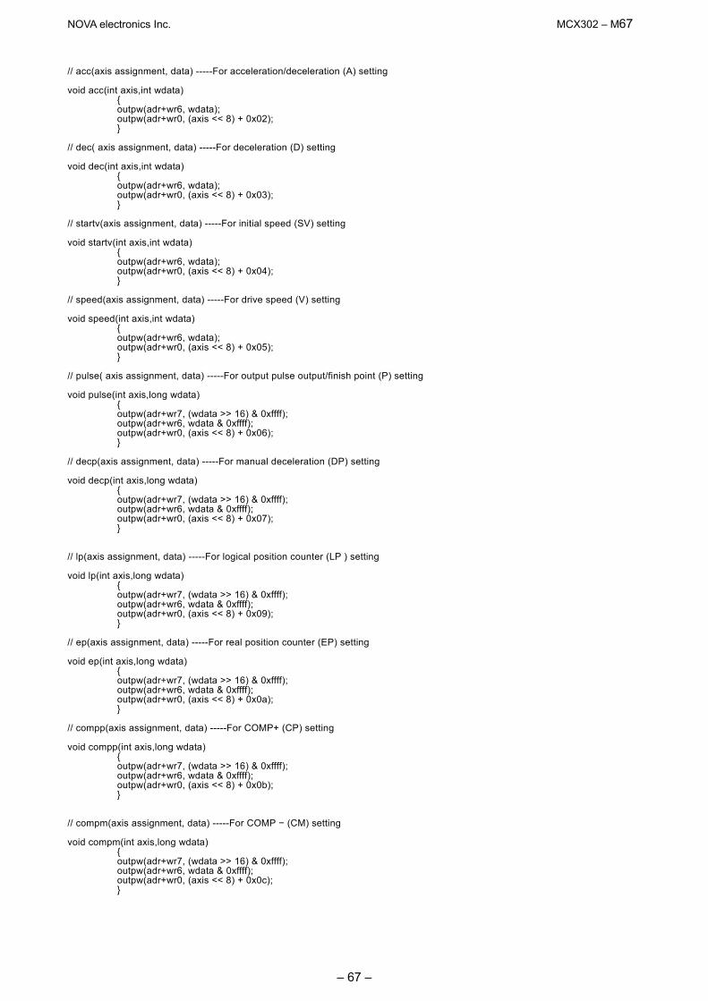
NOVA electronics Inc. MCX302 – M67
– 67 –
// acc(axis assignment, data) -----For acceleration/deceleration (A) setting void acc(int axis,int wdata) outpw(adr+wr6, wdata); outpw(adr+wr0, (axis << 8) + 0x02); // dec( axis assignment, data) -----For deceleration (D) setting void dec(int axis,int wdata) outpw(adr+wr6, wdata); outpw(adr+wr0, (axis << 8) + 0x03); // startv(axis assignment, data) -----For initial speed (SV) setting void startv(int axis,int wdata) outpw(adr+wr6, wdata); outpw(adr+wr0, (axis << 8) + 0x04); // speed(axis assignment, data) -----For drive speed (V) setting void speed(int axis,int wdata) outpw(adr+wr6, wdata); outpw(adr+wr0, (axis << 8) + 0x05); // pulse( axis assignment, data) -----For output pulse output/finish point (P) setting void pulse(int axis,long wdata) outpw(adr+wr7, (wdata >> 16) & 0xffff); outpw(adr+wr6, wdata & 0xffff); outpw(adr+wr0, (axis << 8) + 0x06); // decp(axis assignment, data) -----For manual deceleration (DP) setting void decp(int axis,long wdata) outpw(adr+wr7, (wdata >> 16) & 0xffff); outpw(adr+wr6, wdata & 0xffff); outpw(adr+wr0, (axis << 8) + 0x07); // lp(axis assignment, data) -----For logical position counter (LP ) setting void lp(int axis,long wdata) outpw(adr+wr7, (wdata >> 16) & 0xffff); outpw(adr+wr6, wdata & 0xffff); outpw(adr+wr0, (axis << 8) + 0x09); // ep(axis assignment, data) -----For real position counter (EP) setting void ep(int axis,long wdata) outpw(adr+wr7, (wdata >> 16) & 0xffff); outpw(adr+wr6, wdata & 0xffff); outpw(adr+wr0, (axis << 8) + 0x0a); // compp(axis assignment, data) -----For COMP+ (CP) setting void compp(int axis,long wdata) outpw(adr+wr7, (wdata >> 16) & 0xffff); outpw(adr+wr6, wdata & 0xffff); outpw(adr+wr0, (axis << 8) + 0x0b); // compm(axis assignment, data) -----For COMP − (CM) setting void compm(int axis,long wdata) outpw(adr+wr7, (wdata >> 16) & 0xffff); outpw(adr+wr6, wdata & 0xffff); outpw(adr+wr0, (axis << 8) + 0x0c);
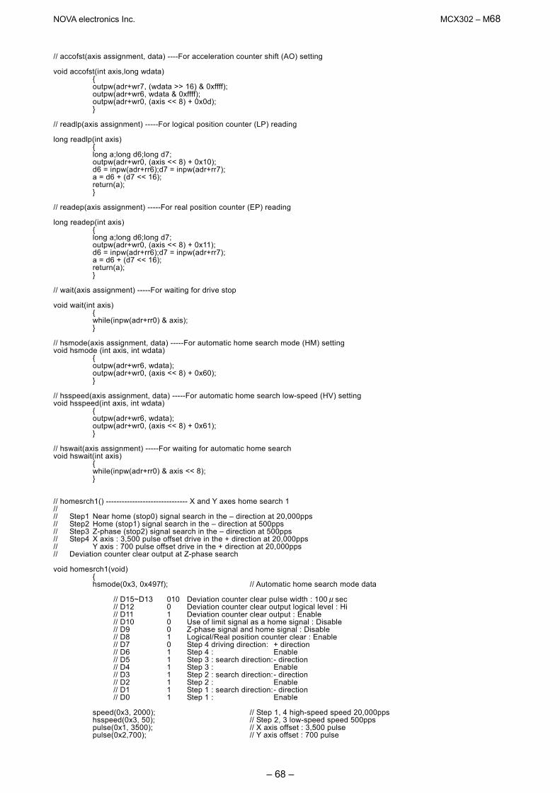
NOVA electronics Inc. MCX302 – M68
– 68 –
// accofst(axis assignment, data) ----For acceleration counter shift (AO) setting void accofst(int axis,long wdata) outpw(adr+wr7, (wdata >> 16) & 0xffff); outpw(adr+wr6, wdata & 0xffff); outpw(adr+wr0, (axis << 8) + 0x0d); // readlp(axis assignment) -----For logical position counter (LP) reading long readlp(int axis) long a;long d6;long d7; outpw(adr+wr0, (axis << 8) + 0x10); d6 = inpw(adr+rr6);d7 = inpw(adr+rr7); a = d6 + (d7 << 16); return(a); // readep(axis assignment) -----For real position counter (EP) reading long readep(int axis) long a;long d6;long d7; outpw(adr+wr0, (axis << 8) + 0x11); d6 = inpw(adr+rr6);d7 = inpw(adr+rr7); a = d6 + (d7 << 16); return(a); // wait(axis assignment) -----For waiting for drive stop void wait(int axis) while(inpw(adr+rr0) & axis); // hsmode(axis assignment, data) -----For automatic home search mode (HM) setting void hsmode (int axis, int wdata) outpw(adr+wr6, wdata); outpw(adr+wr0, (axis << 8) + 0x60); // hsspeed(axis assignment, data) -----For automatic home search low-speed (HV) setting void hsspeed(int axis, int wdata) outpw(adr+wr6, wdata); outpw(adr+wr0, (axis << 8) + 0x61); // hswait(axis assignment) -----For waiting for automatic home search void hswait(int axis) while(inpw(adr+rr0) & axis << 8); // homesrch1() ------------------------------- X and Y axes home search 1 // // Step1 Near home (stop0) signal search in the – direction at 20,000pps // Step2 Home (stop1) signal search in the – direction at 500pps // Step3 Z-phase (stop2) signal search in the – direction at 500pps // Step4 X axis : 3,500 pulse offset drive in the + direction at 20,000pps // Y axis : 700 pulse offset drive in the + direction at 20,000pps // Deviation counter clear output at Z-phase search void homesrch1(void) hsmode(0x3, 0x497f); // Automatic home search mode data // D15~D13 010 Deviation counter clear pulse width : 100μsec // D12 0 Deviation counter clear output logical level : Hi // D11 1 Deviation counter clear output : Enable // D10 0 Use of limit signal as a home signal : Disable // D9 0 Z-phase signal and home signal : Disable // D8 1 Logical/Real position counter clear : Enable // D7 0 Step 4 driving direction: + direction // D6 1 Step 4 : Enable // D5 1 Step 3 : search direction: - direction // D4 1 Step 3 : Enable // D3 1 Step 2 : search direction: - direction // D2 1 Step 2 : Enable // D1 1 Step 1 : search direction: - direction // D0 1 Step 1 : Enable speed(0x3, 2000); // Step 1, 4 high-speed speed 20,000pps hsspeed(0x3, 50); // Step 2, 3 low-speed speed 500pps pulse(0x1, 3500); // X axis offset : 3,500 pulse pulse(0x2,700); // Y axis offset : 700 pulse
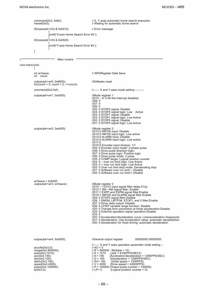
NOVA electronics Inc. MCX302 – M69
– 69 –
command(0x3, 0x62); // X, Y axes automatic home search execution hswait(0x3); // Waiting for automatic home search if((inpw(adr+rr0) & 0x0010) // Error message printf(“X-axis Home Search Error ¥n”); if((inpw(adr+rr0) & 0x0020) printf(“Y-axis Home Search Error ¥n”); // ***************************** Main routine ***************************************************************************** void main(void) int wr3save; // WR3Register Data Save int count; outpw(adr+wr0, 0x8000); //Software reset for(count = 0; count < 2; ++count); command(0x3,0xf); //------ X and Y axes mode setting --------- outpw(adr+wr1, 0x0000); //Mode register 1 //D15 ~ 9: 0 All the interrupt disabled //D8: 0 //D7: 0 //D6: 0 //D5: 0 STOP2 signal: Disable //D4: 0 STOP2 signal logic: Low Active //D3: 0 STOP1 signal: Disable //D3: 0 STOP1 signal logic: Low Active //D2: 0 STOP0 signal: Disable //D1: 0 STOP0 signal logic: Low Active outpw(adr+wr2, 0xe000); //Mode register 2 //D15:0 INPOS input: Disable //D14:0 INPOS input logic: Low active //D13:0 ALARM input: Disable //D12:0 ALARM input logic: Low active //D11:0 //D10:0 Encoder input division: 1/1 //D9: 0 Encoder input mode” 2-phase pulse //D8: 0 Drive pulse direction logic: //D7: 0 Drive pulse logic: Positive logic //D6: 0 Drive pulse mode: 2 pulse //D5: 0 COMP target: Logical position counter //D4: 0 – over run limit logic: Low Active //D3: 0 + over run limit logic: Low Active //D2: 0 Over run limit stop mode: Decelerating stop //D1: 0 Software over run limit-:Disable //D0: 0 Software over run limit+:Disable wr3save = 0x5d00 outpw(adr+wr3, wr3save); //Mode register 3 //D15 ~ 13:010 Input signal filter delay:512μ //D12:1 IN5 ~IN0 signal filter: Enable //D11:1 EXPP and EXPM signal filter:Enable //D10:1 INPOS and ALARM signal filter:Enable //D9: 0 STOP2 signal filter:Disable //D8: 1 EMGN, LMTP/M, STOP1, and 0 filter:Enable //D7: 0 Drive state output: Disable //D6: 0 LP/EP variable range function: Disable //D5: 0 Triangle form prevention at linear acceleration:Disable //D4: 0 External operation signal operation:Disable //D3: 0 //D2: 0 Acceleration/deceleration curve: Lineracceleration (trapezoid) //D1: 0 Deceleration: Use Acceleration value: automatic decelolartion //D0: 0 Deceleration for fixed driving: automatic deceleration outpw(adr+wr4, 0x0000); //General output register 00000000 00000000 //------ X and Y axes operation parameter initial setting -- accofst(0x3,0); // AO = 0 range(0x3,800000); // R = 800000(Multiple = 10) acac(0x3,1010); // K = 1010 (Jerk = 619KPPS/SEC2) acc(0x3,100); // A = 100 (Accleration/deceleration = 125KPPS/SEC) dec(0x3,100); // D = 100 (Deceleration = 125KPPS/SEC) startv(0x3,100); // SV= 100 (Initial speed = 1000PPS) speed(0x3,4000); // V = 4000 (Drive speed = 40000PPS) pulse(0x3,100000); // P = 100000 (Output pulse number = 100000) lp(0x3,0); // LP= 0 (Logical position counter = 0)
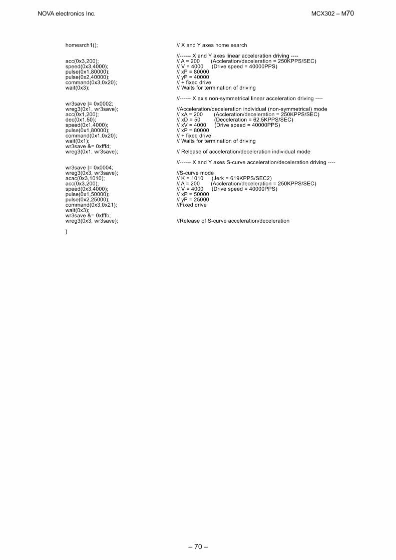
NOVA electronics Inc. MCX302 – M70
– 70 –
homesrch1(); // X and Y axes home search //------ X and Y axes linear acceleration driving ---- acc(0x3,200); // A = 200 (Accleration/deceleration = 250KPPS/SEC) speed(0x3,4000); // V = 4000 (Drive speed = 40000PPS) pulse(0x1,80000); // xP = 80000 pulse(0x2,40000); // yP = 40000 command(0x3,0x20); // + fixed drive wait(0x3); // Waits for termination of driving //------ X axis non-symmetrical linear acceleration driving ---- wr3save |= 0x0002; wreg3(0x1, wr3save); //Acceleration/deceleration individual (non-symmetrical) mode acc(0x1,200); // xA = 200 (Accleration/deceleration = 250KPPS/SEC) dec(0x1,50); // xD = 50 (Deceleration = 62.5KPPS/SEC) speed(0x1,4000); // xV = 4000 (Drive speed = 40000PPS) pulse(0x1,80000); // xP = 80000 command(0x1,0x20); // + fixed drive wait(0x1); // Waits for termination of driving wr3save &= 0xfffd; wreg3(0x1, wr3save); // Release of acceleration/deceleration individual mode //------ X and Y axes S-curve acceleration/deceleration driving ---- wr3save |= 0x0004; wreg3(0x3, wr3save); //S-curve mode acac(0x3,1010); // K = 1010 (Jerk = 619KPPS/SEC2) acc(0x3,200); // A = 200 (Accleration/deceleration = 250KPPS/SEC) speed(0x3,4000); // V = 4000 (Drive speed = 40000PPS) pulse(0x1,50000); // xP = 50000 pulse(0x2,25000); // yP = 25000 command(0x3,0x21); //Fixed drive wait(0x3); wr3save &= 0xfffb; wreg3(0x3, wr3save); //Release of S-curve acceleration/deceleration
NOVA electronics Inc. MCX302 – M71
– 71 –
12. Electrical Characteristics 12.1 DC Characteristics
Absolute Maximum Rated Item Symbol Value Unit
Power Voltage VDD −0.3 ~ +7.0 V Input voltage VIN −0.3 ~ VDD+0.3 V Input Current IIN ±10 mA Preservation Temperature
TSTG −40 ~ +125 °C
Recommend Operation Environment
If the user wishes to operate the IC below 0°C, please make contact with our R&D engineer.
DC Characteristics (Ta = 0 ~ +85°C, VDD = 5V ±5%)
Item Mark Condition Min. Typ. Max. Unit Remark High level input
voltage VIH 2.2 V
Low level input voltage
VIL 0.8 V
High level input current
IIH VIN = VDD −10 10 μA
VIN = 0V −10 10 μA D15~D0 Input signal Low level input current
IIL VIN = 0V −200 −10 μA Input signal besides D15~D0
IOH = −1μA VDD−0.05 V Note 1 IOH = −4mA 2.4 V Output signal besides D15~D0
High level output voltage
VOH IOH = −8mA 2.4 V D15~D0 Output signal IOL = 1μA 0.05 V
IOL = 4mA 0.4 V Output signal besides D15~D0Low level output
voltage VOL
IOL = 8mA 0.4 V D15~D0 Output signal Output leakage
current IOZ VOUT=VDD or 0V −10 10 μA
D15 ~ D0,BUSYN,INTN
Smith hysteresis voltage
VH 0.3 V
Consuming current IDD IIO=0mA,CLK=16MHz 28 50 mA Note1 : BUSYN and INTN output signals have no items for high level output voltage due to the open drain output.
Pin Capacity Item Mark Condition Min. Typ. Max. Unit Remark
Input/ Output capacity
CIO 10 pF D15 ~ D0
Input capacity CI
Ta=25°C, f=1MHz 10 pF Other input pins
Item Symbol Value Unit Power Voltage VDD 4.75 ~ 5.25 V
Ambient Temperature
Ta 0 ~ +85 °C
NOVA electronics Inc. MCX302 – M72
– 72 –
12.2 AC Characteristics (Ta = 0 ~ 85°C, VDD = +5V ± 5%, Output load condition: 85 pF + 1 TTL )
12.2.1 Clock
Symbol Item Min. Max. Unit tCYC CLK Cycle 62.5 nS tWH CLK Hi Level Width 20 nS tWL CLK Low Level Width 20 nS tDR CLK ↑ → SCLK ↑ Delay Time 21 nS tDF CLK ↑ → SCLK ↓ Delay Time 23 nS
12.2.2 Read / Write Cycle
a. The figure shown above is used for 16-bit data bus accessing (H16L8 = Hi). For 8-bit data bus (H16L8 = Low), the address
signals shown in the figure become A3~A0, and data signals become D7~D0.
b. At a read cycle, the data signal (D15~D0) becomes an output state as soon as both RDN and CSN become low and stays in the output state during tDF even if RDN is reset to High. Avoid the occurrence of bus conflict (collision).
Symbol Item Min. Max. Unit
tAR Address Setup Time (to RDN ↓) 0 nS tCR CSN Setup Time (to RDN ↓) 0 nS tRD Output Data Delay Time (from RDN ↓) 29 nS tDF Output Data Hold Time (from RDN ↑) 0 30 nS tRC CSN Hold Time (from RDN ↑) 0 nS tRA Address Hold Time (from RDN ↑) 0 nS
tAW Address Setup Time (to WRN ↓) 0 nS tCW CSN Setup Time (to WRN ↓) 0 nS tWW WRN Low Level Width 50 nS tDW Setup Time of Input Data (to WRN ↑) 32 nS tDH Hold Time of Input Data (from WRN ↑) 0 nS tWC CSN Hold Time (from WRN ↑) 0 nS tWA Address Hold Time (from WRN ↑) 5 nS
CLK Input Signal SCLK Output Signal
CLK CLK
SCLKtCYC
tWH tWLtDR tDF
SCLK will not be output during reset.
CSNA2 -A0
WRNRDN
D15 -D0
Valid Address
Data OutputHi-Z Hi-Z
tCR tRDtAR
tDFtRC
tRA
tCWtAW tWW
tDW tDHtWC
tWA
Valid Address
Read Cycle Write Cycle
Data Input
NOVA electronics Inc. MCX302 – M73
– 73 –
12.2.3 BUSYN Signal
SCLKWRN
BUSYNtDF tWL
Hi- Z
BUSYN becomes low active for maximum 2 SCLK cycles from WRN ↑. During the time, IC cannot accept Read/Write.
Symbol Item Min. Max. Unit tDF WRN ↑ → BUSYN ↓ Delay Time 32 nS tWL BUSYN Low Level Width tCYC×4 +30 nS
tCYC is a cycle of CLK. 12.2.4 SCLK/Output Signal Timing The following output singles are synchronized with SCLK output signal. The level will be changed at SCLK ↑. Output signals : nPP/PLS, nPM/DIR, nDRIVE, nASND, nDSND, nCMPP, and nCMPM.
SCLK
tDD
Output Signal
Symbol Item Min. Max. Unit tDD SCLK ↑ → Output Signal ↑ ↓Delay Time 0 20 nS
12.2.5 Input Pulses
Quadrature Pulses Input Mode (A/B phases)
Up / Down Pulses Input Mode
a. In quadrature pulses input mode, when nECA and nECB input pulses are changed, the value of real position counter will be
reflected in maximum 4 SCLK cycles. b. In UP/DOWN pulse input mode, the value of real position counter will be reflected in maximum 4 SCLK cycles from nPPIN and nPMIN input↑.
Symbol Item Min. Max. Unit tDE nECA and nECB Phase Difference Time tCYC×2 +20 nS tIH nPPIN and nPMIN Hi Level Width tCYC×2 +20 nS tIL nPPIN and nPMIN Low Level Width tCYC×2 +20 nS
tICYC nPPIN and nPMIN Cycle tCYC×4 +20 nS tIB nPPIN ↑ nPMIN ↑ between Time tCYC×4 +20 nS
tCYC is a cycle of CLK.
nECAnECB
tDE tDE tDE tDE tDE tDE tDE tDE
Count downCount up
nPPIN
nPMINtIH tIL tIB tIH tIL
tICYC tICYC
NOVA electronics Inc. MCX302 – M74
– 74 –
12.2.6 General Purpose Input / Output Signals The figure shown at the lower left hand side illustrates the delay time when input signals nSTOP2 ~ 0, nIN5 ~ 0, nEXPP, nEXPM, nINPOS, and nALARM are read through RR4 and RR5 registers. (When filter is disabled.) The figure shown at the lower right hand side illustrates the delay time when writing general output signal data into WR4.
Symbol Item Min. Max. Unit tDI Input Signal → Data Delay Time 32 nS tDO WRN ↑ → nOUT7~0 Setup Time 32 nS
Input Signal
RDND15~0
tDInOUT7~0
tDO
WRN
D15~0
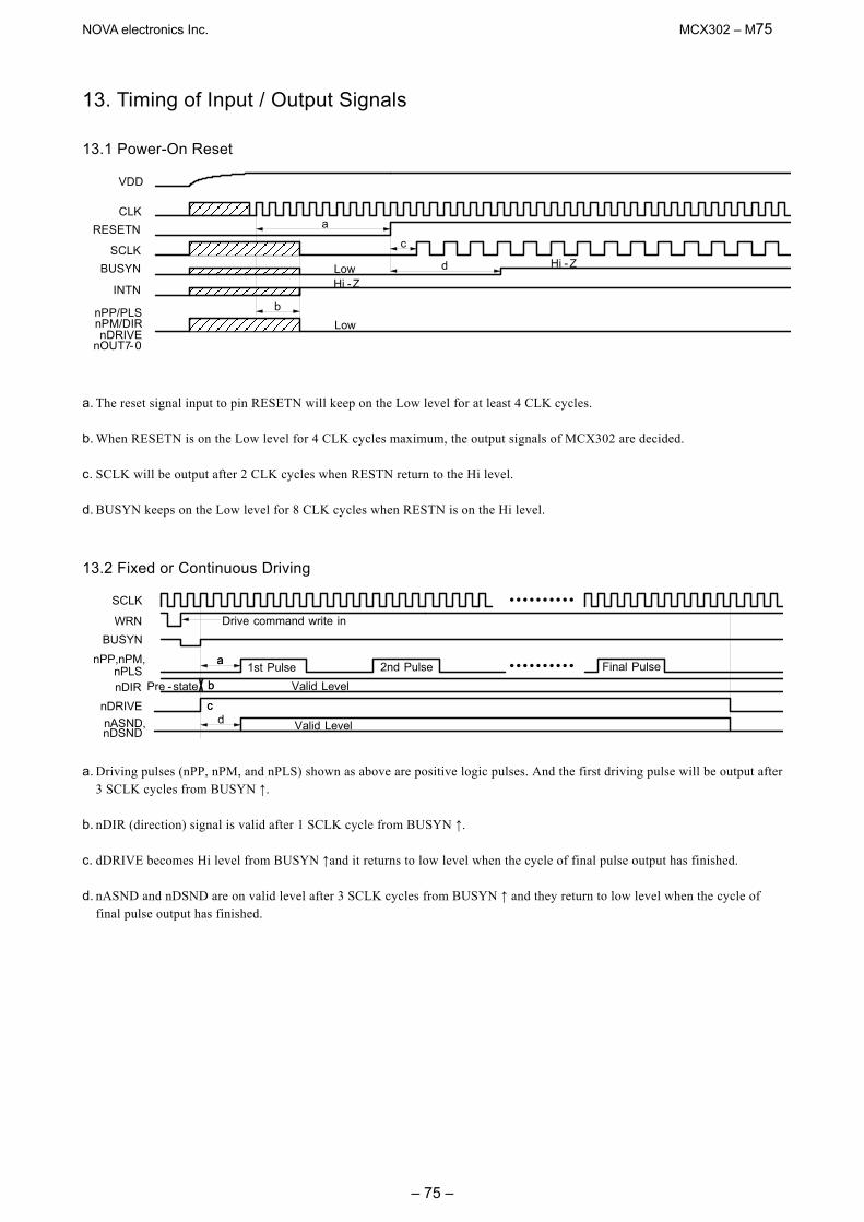
NOVA electronics Inc. MCX302 – M75
– 75 –
13. Timing of Input / Output Signals
13.1 Power-On Reset
a. The reset signal input to pin RESETN will keep on the Low level for at least 4 CLK cycles. b. When RESETN is on the Low level for 4 CLK cycles maximum, the output signals of MCX302 are decided. c. SCLK will be output after 2 CLK cycles when RESTN return to the Hi level. d. BUSYN keeps on the Low level for 8 CLK cycles when RESTN is on the Hi level.
13.2 Fixed or Continuous Driving
a. Driving pulses (nPP, nPM, and nPLS) shown as above are positive logic pulses. And the first driving pulse will be output after
3 SCLK cycles from BUSYN ↑. b. nDIR (direction) signal is valid after 1 SCLK cycle from BUSYN ↑. c. dDRIVE becomes Hi level from BUSYN ↑and it returns to low level when the cycle of final pulse output has finished. d. nASND and nDSND are on valid level after 3 SCLK cycles from BUSYN ↑ and they return to low level when the cycle of
final pulse output has finished.
CLKRESETN
BUSYN
nPP/PLSnPM/DIR
nOUT7-0
INTN
VDD
Low Hi -Z
Hi -Z
nDRIVELow
SCLK
a
b
c
d
1st Pulse 2nd Pulse Final Pulse
Pre -state Valid Level
SCLK
WRNBUSYN
nPP,nPM,
nDIRnDRIVEnASND, Valid Level
nPLS
nDSND
Drive command write in
a
b
cd
a
b
c
NOVA electronics Inc. MCX302 – M76
– 76 –
13.3 Start Driving after Hold Command
a. The pulses (nPP, nPM, and nPLS) of each axis will start outputting after 3 SCLK cycles when BUSYN is ↑. b. nDRIVE will become Hi level when BUSYN is ↑ for each axis.
13.4 Sudden Stop The following figure illustrates the timing of sudden stop. The sudden stop input signals are EMGN, nLMTP/M (When the sudden stop mode is engaged), and nALARM. When sudden stop input signal becomes active, or the sudden stop command is written, it will stop the output of pulses immediately. The width of external signals input for sudden stop must be more than 1 SCLK cycle. The stop function will not be active if the width is less 1 SCLK cycle.
An instant stop input signal is loaded into IC by SCLK↑. When the input signal filter is enabled, the input signal will be delayed according to the constant value at filtering.
13.5 Decelerating Stop The following figure illustrates the timing of decelerating stop input signal and decelerating commands. The decelerating stop signal are nSTOP2 ~ 0 and nLMTP/M (When the decelerating mode is engaged). When speed decelerating signals become active, or the decelerating stop command is written, the decelerating stop function will be performed.
If the input signal filter is disabled, the input signal is delayed according to the value of the time constant of the filter.
Start Driving after Hold CommandDrive Command
SCLKWRN
BUSYNnPP,nPM,
nPLSnDRIVE
1st Pulse 2nd Pulsea
b
SCLKSignal,
Command WRN
nPP,nPM,nPLSnDRIVE
Active
Signal,Command WRN
nPP,nPM,nPLS
nDSND
Active
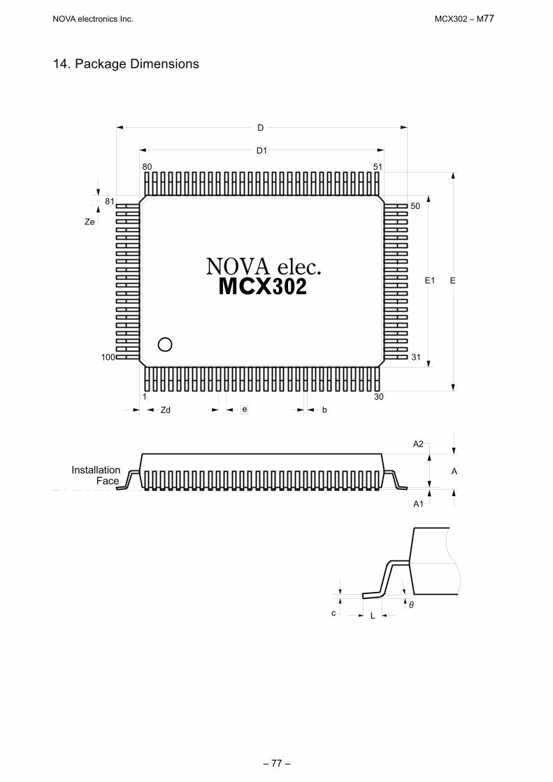
NOVA electronics Inc. MCX302 – M77
– 77 –
14. Package Dimensions
Installation
θc L
A2
A1
A
Zd e b
Ze
100
1 30
31
50
5180
81
D
D1
EE1NOVA elec.MCX302
Face
NOVA electronics Inc. MCX302 – M78
– 78 –
Size mm (inch) Symbol
Minimum Standard MaximumDescription
A — — 3.05
(0.120) Height from the installation face to the top end of the package main unit
A1 0.09
(0.004) 0.19
(0.007) 0.29
(0.011) Height from the installation face to the bottom end of the package main unit
A2 2.5
(0.098) 2.7
(0.106) 2.9
(0.114) Height from the top to the bottom of the package main unit
b 0.2
(0.008) 0.3
(0.012) 0.4
(0.016) Pin width
c 0.10
(0.004) 0.15
(0.006) 0.25
(0.010) Pin thickness
D 23.5
(0.925) 23.8
(0.937) 24.1
(0.949) Maximum length in the package length direction including pins
D1 19.8
(0.780) 20.0
(0.787) 20.2
(0.795) Length of the package main unit excluding pins
E 17.5
(0.689) 17.8
(0.701) 18.1
(0.713) Maximum length in the package width direction including pin
E1 13.8
(0.543) 14.0
(0.551) 14.2
(0.559) Width of the package main unit excluding pins
e 0.65
(0.026) Pin pitch standard size
L 0.6
(0.024) 0.8
(0.031) 1.0
(0.039) Length of the flat section of the pins that contacts the installation face
Zd — 0.575
(0.023) —
Length from the center of the outer-most pin to the outer-most pin section of the package main unit in the length direction
Ze — 0.825
(0.032) —
Length from the center of the outer-most pin to the outer-most pin section of the package main unit in the width direction
θ 0° — 10° Angle of the pin flat section for the installation face
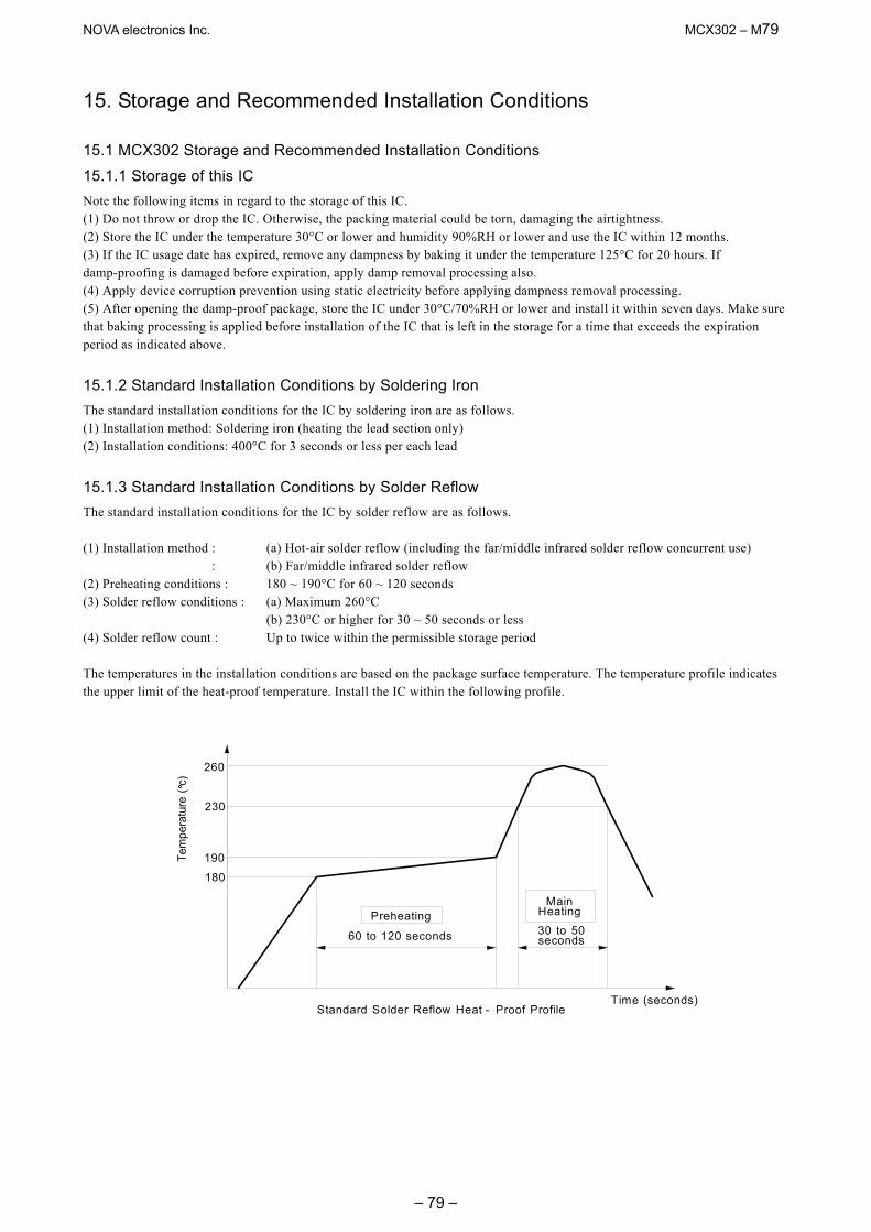
NOVA electronics Inc. MCX302 – M79
– 79 –
15. Storage and Recommended Installation Conditions
15.1 MCX302 Storage and Recommended Installation Conditions
15.1.1 Storage of this IC Note the following items in regard to the storage of this IC. (1) Do not throw or drop the IC. Otherwise, the packing material could be torn, damaging the airtightness. (2) Store the IC under the temperature 30°C or lower and humidity 90%RH or lower and use the IC within 12 months. (3) If the IC usage date has expired, remove any dampness by baking it under the temperature 125°C for 20 hours. If damp-proofing is damaged before expiration, apply damp removal processing also. (4) Apply device corruption prevention using static electricity before applying dampness removal processing. (5) After opening the damp-proof package, store the IC under 30°C/70%RH or lower and install it within seven days. Make sure that baking processing is applied before installation of the IC that is left in the storage for a time that exceeds the expiration period as indicated above.
15.1.2 Standard Installation Conditions by Soldering Iron The standard installation conditions for the IC by soldering iron are as follows. (1) Installation method: Soldering iron (heating the lead section only) (2) Installation conditions: 400°C for 3 seconds or less per each lead
15.1.3 Standard Installation Conditions by Solder Reflow The standard installation conditions for the IC by solder reflow are as follows. (1) Installation method : (a) Hot-air solder reflow (including the far/middle infrared solder reflow concurrent use)
: (b) Far/middle infrared solder reflow (2) Preheating conditions : 180 ~ 190°C for 60 ~ 120 seconds (3) Solder reflow conditions : (a) Maximum 260°C (b) 230°C or higher for 30 ~ 50 seconds or less (4) Solder reflow count : Up to twice within the permissible storage period The temperatures in the installation conditions are based on the package surface temperature. The temperature profile indicates the upper limit of the heat-proof temperature. Install the IC within the following profile.
260
230
190
180
60 to 120 seconds 30 to 50seconds
MainHeatingPreheating
Time (seconds)
Tem
pera
ture
(c)
Standard Solder Reflow Heat - Proof Profile
NOVA electronics Inc. MCX302 – M80
– 80 –
16. Specifications
Control Axis 2 axes Data Bus 16/8 bits selectable Drive Pulses Output (When CLK = 16 MHz)
Pulse Output Speed Range 1 ~ 4MPPS Pulse Output Accuracy within ± 0.1% (according to the setting speed) S-curve Jerk 954 ~ 62.5 x 10⁶ PPS/S2 (Multiple = 1) 477 x 103 ~ 31.25 x 10⁹PPS/S2 (Multiple = 500) Accelerating / Decelerating Speed 125 ~ 1 x 10⁶ PPS/S (Multiple = 1) 62.5×10³ ~ 500 x 106 PPS/S (Multiple = 500) Initial Speed 1 ~ 8,000PPS (Multiple = 1) 500PPS ~ 4×10⁶ PPS (Multiple = 500) Drive Speed 1 ~ 8,000PPS (Multiple = 1) 500PPS ~ 4×10⁶ PPS (Multiple = 500) Output-pulse Number 0 ~ 268,435,455 (fixed drive) Speed Curve Constant speed, linear acceleration, parabola S-curve acceleration/deceleration drive Fixed Drive Deceleration Mode auto (non-symmetrical trapezoidal acceleration is also allowed) / manual Output-pulse numbers and drive speeds changeable during the driving Independent 2-pulse system or 1-pulse 1-direction system selectable Logical levels of drive pulse selectable
Encoder Input A/B quadrature pulse style or Up/Down pulse style selectable Pulse of 1, 2 and 4 divisions selectable (A/B quadrature pulse style)
Position Counter Logic Position Counter (for output pulse) range −2,147,483,648 ~ +2,147,483,647 Real Position Counter (for feedback pulse) range −2,147,483,648 ~ +2,147,483,647 Data read and write possible
Comparison Register COMP + Register Position comparison range −1,073,741,824 ~ +1,073,741,824 COMP − Register Position comparison range −1,073,741,824 ~ +1,073,741,824 Status and signal outputs for the comparisons of position counters Software limit functioned
Automatic home search Automatic execution of Step 1 (high-speed near home search) → Step 2 (low-speed home search) → Step 3 (low-speed
encoder Z-phase search) → Step 4 (high-speed offset drive). Enable/Disable of each step and search direction selectable
Deviation counter clear output : Clear pulse width within the range of 10μ ~ 20msec and logical level selectable
Interrupt (Interpolations Excluded) The factors of occurring interrupt: ..the start / finish of a constant-speed drive during the acceleration / deceleration driving ..the end of the driving ..the volume of position counter ≥ the volume of COMP− ..the volume of position counter < the volume of COMP− ..the volume of position counter ≥ the volume of COMP+ ..the volume of position counter < the volume of COMP+ Enable / disable for these factors selectable
External Signal for Driving EXPP and EXPM signals for fixed pulse / continuous drive Driving in MPG mode (encoder input)
External Deceleration / Sudden Stop Signal STOP0 ~ 2 3 points for each axis Enable / disable and logical levels selectable
Servo Motor Input Signal ALARM (Alarm), INPOS (In Position Check), DCC (Deviation counter clear output) Enable / disable and logical levels selectable
General Input / Output Signal IN0 ~ 5 6 points for each axis (wherein 4 points use with multichip interpolation signal pin) OUT0 ~ 7 8 points for each axis (wherein it uses with drive status output pin and OUT0 uses with deviation counter
clear output pin)
NOVA electronics Inc. MCX302 – M81
– 81 –
Driving Status Signal Output
DRIVE (drive pulse outputting), ASND (speed accelerating), CNST (constant driving), DSND (speed decelerating), CMPP (position ≥ COMP+), CMPM (position < COMP−), ACASND (acceleration/deceleration speed increase), ACDSND (acceleration/deceleration speed decrease)
Drive status and status registers readable
Limit Signals Input 1 point, for each + and − side Logical levels and decelerating / sudden stop selectable
Emergency Stop Signal Input EMG, 1 point in all axes Sudden stop the drive pulse of all axes when on Low level
Contents of integral type filters Equipped with integral filters in the input column of each input signal. One time constant can be selected from eight
types.
Electrical Characters Temperature Range for Operation 0 ~ + 85°C (32°F ~185°F) Power Voltage +5V ± 5 % Input / Output Signal Level CMOS, TTL connectable Clock pulse 16,000 MHz (Standard)
Package 100-pin plastic QFP, pitch = 0.65mm Dimension : 23.8 × 17.8 × 3.05 mm

NOVA electronics Inc. MCX302 - A1
– A1 –
Appendix A Profile of Speed curve The following curves are based on the test records from MCX302 output drive pulses and speed curve traces. The perfect S curve acceleration / deceleration is the curve drive, without linear acceleration / deceleration, before the appointed drive speed is reached. Partial S curve acceleration / deceleration is with a period of linear acceleration / deceleration before the appointed drive speed is reached.
20K
20K
R=800000 (Multiple: 10), K=700, (A=D=200), SV=100, V=4000, A0=0Auto Deceleration mode
Jerk= 893K PPS/SEC2 (Acceleration= 250K PPS/SEC)Initial speed= 1000 PPS Drive speed= 40K PPS
Output Pulse P= 50000 P= 30000P= 2000P= 20000P= 10000
P= 5000
1.0 2.0sec
20K
40K PPS
40KPPS Perfect S curve acceleration/deceleration
R=800000 (Multiple: 10), K=300, (A=D=150), SV=100, V=4000, A0=0Auto Deceleration mode
Jerk= 2083K PPS/SEC2 Acceleration= 188K PPS/SEC Initial speed= 1000 PPS Drive speed= 40K PPS
Output Pulse P= 50000 P= 30000P= 20000P= 10000 P= 5000
40KPPS Partial S curve acceleration/deceleration
20K
40K PPS
1.0 2.0sec

NOVA electronics Inc. MCX302 - A2
– A2 –
R=8000000 (Multiple: 1), K=2000, (A=D=500), SV=100, V=8000, A0=0Auto Deceleration mode
Jerk= 31K PPS/SEC2 (Acceleration= 62.5K PPS/SEC)Initial speed= 100 PPS Drive speed= 8000 PPS
8000PPS Perfect S curve acceleration/deceleration
2.0 4.0sec
4K
8K PPS
Output Pulse P= 20000 P= 10000P= 5000P= 2000
R=8000000 (Multiple: 1), K=1000, A=D=100, SV=100, V=8000, A0=0Auto Deceleration mode
Jerk= 62.5K PPS/SEC2 (Acceleration= 12.5K PPS/SEC)Initial speed= 100 PPS Drive speed= 8000 PPS
8000PPS Partial S curve acceleration/deceleration
2.0 4.0sec
4K
8K PPS
Output Pulse P= 20000 P= 10000P= 5000 P= 2000
R=80000 (Multiple: 100), K=2000, (A=D=100), SV=10, V=4000, A0=0Auto Deceleration mode
Jerk= 3.13M PPS/SEC2 (Acceleration= 1.25M PPS/SEC)Initial speed= 1000 PPS Drive speed= 400K PPS
400KPPS Perfect S curve acceleration/deceleration
1.0 2.0sec
200K
400K PPS
Output Pulse P= 400000P= 200000P= 100000P= 50000
R=80000 (Multiple: 100), K=500, (A=D=100), SV=10, V=4000, A0=0 Auto Deceleration mode
Jerk= 12.5M PPS/SEC2 (Acceleration= 1.25M PPS/SEC)Initial speed= 1000 PPS Drive speed= 400K PPS
400KPPS Partial S curve acceleration/deceleration
1.0 2.0sec
200K
400K PPS
Output Pulse P= 400000P= 200000P= 100000 P= 20000
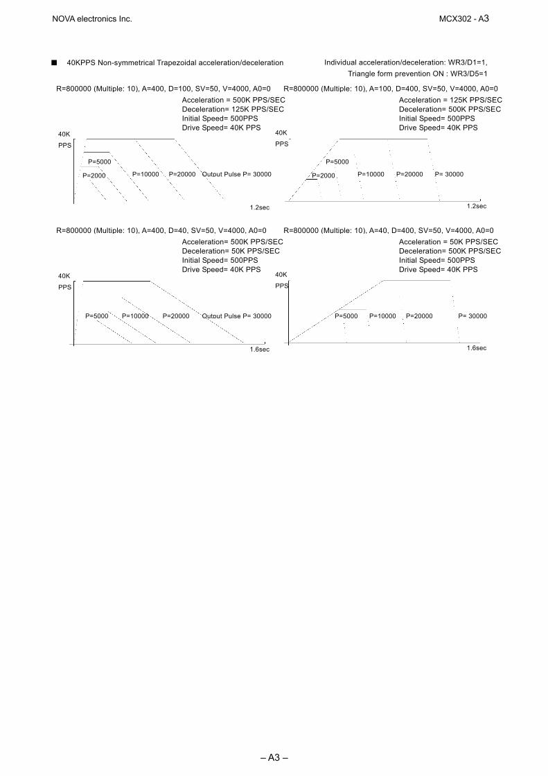
NOVA electronics Inc. MCX302 - A3
– A3 –
R=800000 (Multiple: 10), A=400, D=100, SV=50, V=4000, A0=0Acceleration = 500K PPS/SECDeceleration= 125K PPS/SECInitial Speed= 500PPS Drive Speed= 40K PPS
40KPPS Non-symmetrical Trapezoidal acceleration/deceleration
Output Pulse P= 30000P=20000 P=10000
P=5000
P=2000
1.2sec
40K
PPS
Acceleration = 125K PPS/SECDeceleration= 500K PPS/SECInitial Speed= 500PPS Drive Speed= 40K PPS
Individual acceleration/deceleration: WR3/D1=1,Triangle form prevention ON : WR3/D5=1
P= 30000P=20000 P=10000
P=5000
P=2000
1.2sec
40K
PPS
R=800000 (Multiple: 10), A=100, D=400, SV=50, V=4000, A0=0
R=800000 (Multiple: 10), A=400, D=40, SV=50, V=4000, A0=0Acceleration= 500K PPS/SECDeceleration= 50K PPS/SECInitial Speed= 500PPS Drive Speed= 40K PPS
Output Pulse P= 30000P=20000 P=10000 P=5000
1.6sec
40K
PPS
Acceleration = 50K PPS/SECDeceleration= 500K PPS/SECInitial Speed= 500PPS Drive Speed= 40K PPS
P= 30000P=20000 P=10000 P=5000
1.6sec
40K
PPS
R=800000 (Multiple: 10), A=40, D=400, SV=50, V=4000, A0=0
NOVA electronics Inc. MCX302 - B1
– B1 –
Appendix B Important notice
Ⅰ Notice for fixed pulse or continuous pulse driving in S-curve acceleration/deceleration
[Symptom]
When using fixed pulse driving or continuous pulse driving in S-curve acceleration/deceleration, driving is performed at an initial speed without acceleration.
[Occurrence Condition]
1. When fixed pulse driving or continuous pulse driving is performed in S-curve acceleration / deceleration mode
(WR3/D2=1), 2. the value of (Drive speed V - Initial speed SV) is lower than the half value of (V-SV) which is driven just before. 3. And in the driving just before, when ACC counter (which is used in S-curve acceleration / deceleration driving in
the IC) is not returned to 0 at the end of driving.
[Workaround]
Before start of driving, use following steps to workaround this behavior, with an inspection command to clear the internal ACC counter. This command is not described in the manual. When fixed pulse driving or continuous pulse driving is performed in S-curve acceleration/ deceleration mode (WR3/D2=1), write 44h command just before all the drive commands are written. (Example) Set mode for S-curve acceleration/deceleration Set Range (R) Set Jerk (K) Set Acceleration (A) Set Initial speed (SV) Set Drive speed (V) Set Output pulse number (P)
WR0 Axis assignment+44h ;Command for workaround
WR0 Axis assignment+20h ;Fixed pulse drive in the +direction
Waits for termination of driving
|
Set Output pulse number (P)
WR0 Axis assignment+44h ;Command for workaround
WR0 Axis assignment+21h ;Fixed pulse drive in the –direction
NOVA electronics Inc. MCX302 - B2
– B2 –
Waits for termination of driving
|
Change Drive speed (V)
WR0 Axis assignment+44h ;Command for workaround
WR0 Axis assignment+22h ;Continuous pulse drive in the +direction
Waits for termination of driving
Ⅱ Notice for Compare Register
[Symptom]
Although Range of Position Comparison between Position Counter and Compare Register(COMP+,-) is shown as -2,147,483,648 to +2,147,483,647 (signed 32-bit)on User’s Manual, actually it is -1,073,741,824 to +1,073,741,823(signed 31-bit)due to the defect of IC.
[Workaround]
Don’t compare the values over the range such as -1,073,741,824 to +1,073,741,823.
NOVA electronics Inc. MCX302 - B3
– B3 –
Ⅲ Notice for Fixed pulse driving in S-curve acceleration/deceleration
[Symptom]
When using fixed pulse driving in S-curve acceleration/deceleration, if one of the following occasions ① to ④ is taken just before finishing driving, pulse may be continuously outputted depending on setting value of parameters.
speed
time
drive speed
initial speed
one of ①~④ is excuted here. Figure 1. Speed profile of fixed pulse driving in S-curve acceleration/deceleration
① When decelerating stop command (26h) was given just before finishing driving ② When setting stop mode of hardware limit(nLMTP/M signal) as decelerating stop(WR2/D2=1), driving is
started and hardware limit of progress direction becomes active just before finishing driving ③ When software limit is enabled(WR2/D0,1=1), driving is started and hardware limit of progress direction
becomes active just before finishing driving ④ When nSTOP(2~0)signals are enabled(WR1/D5,3,1), fixed pulse driving is started and those signals become
active just before finishing driving ・ This trouble won’t happen when trapezoidal(liner) acceleration/deceleration drive or constant speed drive is
performed. ・ This trouble won’t be happened when continuous pulse driving in S-curve acceleration/deceleration. ・ This trouble won’t happen when any of Sudden stop command, EMGN signal, LMT signal of Sudden stop and
ALARM signal is outputted. Fixed pulse driving in S-curve acceleration/deceleration is performed as that driving speed and initial speed becomes equal and acceleration becomes zero(0) when driving finished ,which means all pulse outputted. But it’s impossible to make driving speed & initial speed equal and acceleration zero(0) in all combinations of parameters because of the problem of calculation accuracy. This trouble will happen if it is in the above mentioned occasion ①, ②, ③ or ④ as the factors of deceleration stop accidentally and driving speed hasn’t reached initial speed yet but acceleration has become zero(0) showing on Figure 2.

NOVA electronics Inc. MCX302 - B4
– B4 –
speed
time
time
initial speed
0
driving speed hasn't reached initial one yet.
acceleration becomes0.
acceleration
Figure 2. Driving speed and acceleration just before driving completion
Deceleration status of accelerating(ASND), constant speed driving(CNST) and decelerating(DSND) can be read out according to RR1 resister of IC. The status is shown as Figure 3. as below ;
Figure 3. Status of
deceleration shown by RR1 resister
The timing when the trouble may possibly happen is shown as “d” on Figure 3. At this time, status of deceleration is constant speed
driving(CNST=1). Besides in case the trouble such as outputting pulse continuously happens, all of ASND, CNST and DSND will become 0 even though it’s driving(RR0/nDRV=1).
[Workaround] 1 When deceleration stop command(26h) is executed【Case ①】 Basically once deceleration starts, it isn’t necessary to execute deceleration stop command. Therefore deceleration stop command should be prohibit. See nRR1/D4(DSND) normally to know it’s decelerating or not. Timing when the trouble happens is in “d” as shown on Figure 3 if deceleration stop command is executed. In “d” DSND status bit is 0 and CNST status bit is 1. Therefore the following two(2) solutions will be proposed.
(1) When interruption from IC can be used When deceleration starts, interruption will be occurred to prohibit execution of deceleration stop command(26h) until driving completion. Flag of prohibition against deceleration stop command is prepared and it will be clear before driving starts. Enable constant speed area completion interruption(WR1/D13(C-END)=1). Fixed pulse driving starts and if interruption is occurred, read RR3/D5(C-END) within interruption process routine and status bit is 1, constant speed area is completed which is same as deceleration starts. So make flag of prohibition against deceleration stop
speed
timeacceleration
time
driving speed
initial speed
0
RR1/D2 ASNDRR1/D3 CNSTRR1/D4 DSNDRR0/D0~3 nDRV
a b cd
e
1
0
0
0

NOVA electronics Inc. MCX302 - B5
– B5 –
command 1. Besides it is possible that CNST(constant speed area) will occur just before driving completion. Then return WR1/D13 status bit from 1 to 0 in order to prevent interruption. On the other hand, within task, see flag and if it’s 1, don’t execute deceleration stop command.
(2) When interruption can’t be used Terms when deceleration stop command should be executed in accelerating and constant speed driving such as “a” and “b” on Figure 3. Status of deceleration for both “d” (timing when the trouble happens) and “b” (constant speed driving) is same as constant speed driving as shown on Figure 3. But there is difference of driving speed between two. Driving speed in “b” is near that of setting driving speed. Driving speed in “d” is near that of initial speed. Therefore before driving starts, prepare judgmental speed which is middle one between initial speed and setting speed ((Driving speed - initial speed)/2 + initial speed). When execute deceleration stop command during driving, make sure status is accelerating(ASND=1) or constant speed driving(CNST=1) and driving speed is same or faster than judgmental speed. 2 Hardware limit(nLMTP/M signal) at deceleration stop mode【Case ②】 Basically use hardware limit(nLMTP/M signal) at Sudden stop mode when fixed pulse driving in S-curve acceleration/deceleration. Out of necessity, when use hardware limit at deceleration stop mode, prepare the following measures. If multi-axes are controlled in the same time, (1) When interruption from IC can be used is effective. (1) When interruption from IC can be used Constant speed area (“b” area) on Figure 3 is set as occurrence factor of interruption. But this interruption is also happened when there is “d” area just before driving stops on Figure 3 such as when driving speed reaches initial speed or when acceleration becomes 0(zero). There should occur “d” area definitely if the trouble is happened just before driving stops, driving speed hasn’t reached initial speed yet, acceleration becomes 0 and decelerating stop requirement is executed. The measure is to judge if the trouble happens or not in the timing of interruption when “d” area ends. Make constant speed area finishing interruption of IC active(WR1/D13(C-END)=1). Start fixed pulse driving in S-curve acceleration/deceleration and when interruption is happened, interruption processing is executed as follows;

NOVA electronics Inc. MCX302 - B6
– B6 –
INTERRUPTION PROCESSING
nRR3/D5(C-END)=1?
nRR1/D4(DSND)=1?
RR0/D0(X AXIS)=0?
nRR1/D12orD13=1?
nRR1/D2=D3=D4=0?
SUDDEN STOP COMMAND(27h)
PROCESSING FINISHED
① GOES OUT CONSTANT SPEED AREA?
② DECELERATING AREA?
③ DRIVING FINISHES?
④ FORWARD LIMIT IS ON?
⑤ ASND=CNST=DSND=0?
⑥ JUDGED AS TROUBLE HAPPENS
This shows the interruption when driving goes into decelerating area (c) from constant speed area (b) is normal. Make driving finished as it goes.
This shows the interruption when driving has finished normally in area (d). Make driving finished as it goes.
During driving, backward limit never be on. So RR1/D12, D13 won’t be 1 due to backward limit.
no OTHER INTERRUPTION FACTORS
no
no
no
no
yes
yes
yes
yes
① Check if driving goes out constant speed area or not. If RR3/D5(C-END) bit of driving axis is 0, there are other
interruption factors. Execute those interruption processing. ② Check if driving goes into decelerating area or not. If it’s RR1/D4(DSND)=1, make it finished as it goes because
driving goes into “c” area from “b” area on Figure 3. If it’s RR1/D4(DSND)=0, move it to ③ processing because driving has gone out “d” area.
③ Check if driving has finished or not. If it’s finished, make it finished as it goes because driving has finished normally. But if it’s not finished yet, surely trouble have happened because status is shown as it’s still driving even though driving has gone out “d” area.
④ Check if hard limit is ON or OFF. Since RR1/D12 bit becomes 1 if + limit is ON and RR1/D13 bit becomes 1 if – limit is ON, if it’s D12=1 or D13=1, judge forward limit is ON.
⑤ If trouble has happened, it becomes ASND=CNST=DSND=0. Check them all. ⑥ Execute sudden stop command(27h).
NOVA electronics Inc. MCX302 - B7
– B7 –
(2) When interruption can’t be used In “d” area on Figure 3, if forward limit is active, the trouble will happen, more exactly saying, it will seldom happen. There isn’t any method to avoid it before it happens. So immediately after the trouble happens, take means to stop driving. If the trouble happens (“e” area on Figure 3), status keeps driving(RR0/nDRV=1), status of acceleration/deceleration is 0 in ASND, CNST, DSND. This is completely abnormal state. So the example of measure is shown as follows;
DRIVING STARTS
KEEP DRIVING?
FORWARD LIMIT ON?
KEEP DRIVING?
ASND=CNST=DSND=0?
SUDDEN STOP COMMAND(27h)
KEEP DRIVING?
DRIVING COMPLETION
RR0/DRV bit
RR1/D12,13
RR1/ASND,CNST,DSND bit
no
no
no
no
no
yes
yes
yes
yes
yes
When start fixed pulse driving in S-curve acceleration/deceleration, always read out status of progress directional hardware limit(RR1/D12,D13) with timer interruption. If limit signal becomes active, read out bit status of ASND(D2), CNST(D3) and DSND(D4) in RR1 resister and execute Sudden stop command(27h) one time only if all those 3 bits are 0. 3 Software limit【Case ③】 In fixed pulse driving, the target position(goal) can be calculated from present position(logical position counter value) and number of output pulse. If target position is over value of software limit, don’t drive to avoid the trouble.
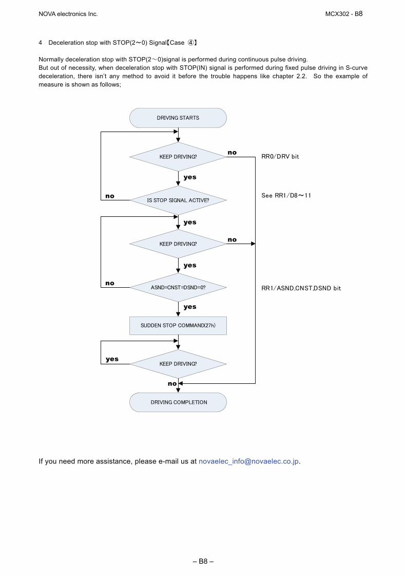
NOVA electronics Inc. MCX302 - B8
– B8 –
4 Deceleration stop with STOP(2~0) Signal【Case ④】 Normally deceleration stop with STOP(2~0)signal is performed during continuous pulse driving. But out of necessity, when deceleration stop with STOP(IN) signal is performed during fixed pulse driving in S-curve deceleration, there isn’t any method to avoid it before the trouble happens like chapter 2.2. So the example of measure is shown as follows;
DRIVING STARTS
KEEP DRIVING?
IS STOP SIGNAL ACTIVE?
KEEP DRIVING?
ASND=CNST=DSND=0?
SUDDEN STOP COMMAND(27h)
KEEP DRIVING?
DRIVING COMPLETION
RR0/DRV bit
See RR1/D8~11
RR1/ASND,CNST,DSND bit
no
no
no
no
no
yes
yes
yes
yes
yes
If you need more assistance, please e-mail us at [email protected].
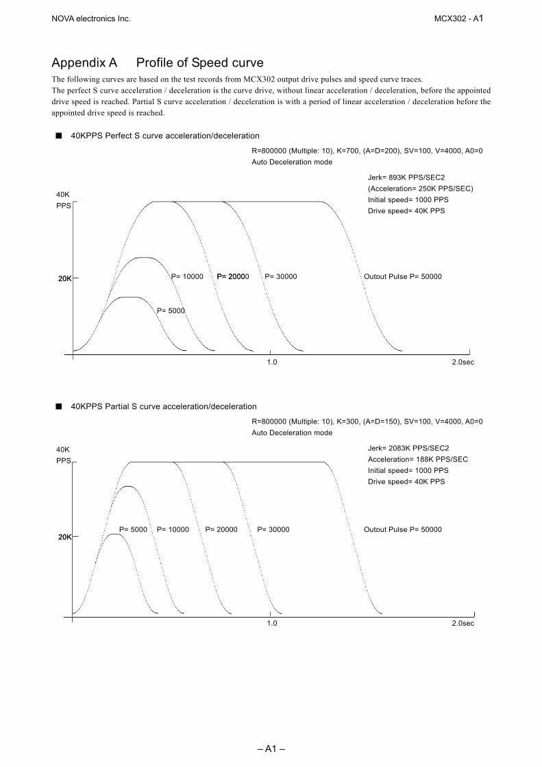
NOVA electronics Inc. MCX302 - A1
– A1 –
Appendix A Profile of Speed curve The following curves are based on the test records from MCX302 output drive pulses and speed curve traces. The perfect S curve acceleration / deceleration is the curve drive, without linear acceleration / deceleration, before the appointed drive speed is reached. Partial S curve acceleration / deceleration is with a period of linear acceleration / deceleration before the appointed drive speed is reached.
20K
20K
R=800000 (Multiple: 10), K=700, (A=D=200), SV=100, V=4000, A0=0Auto Deceleration mode
Jerk= 893K PPS/SEC2 (Acceleration= 250K PPS/SEC)Initial speed= 1000 PPS Drive speed= 40K PPS
Output Pulse P= 50000 P= 30000P= 2000P= 20000P= 10000
P= 5000
1.0 2.0sec
20K
40K PPS
40KPPS Perfect S curve acceleration/deceleration
R=800000 (Multiple: 10), K=300, (A=D=150), SV=100, V=4000, A0=0Auto Deceleration mode
Jerk= 2083K PPS/SEC2 Acceleration= 188K PPS/SEC Initial speed= 1000 PPS Drive speed= 40K PPS
Output Pulse P= 50000 P= 30000P= 20000P= 10000 P= 5000
40KPPS Partial S curve acceleration/deceleration
20K
40K PPS
1.0 2.0sec
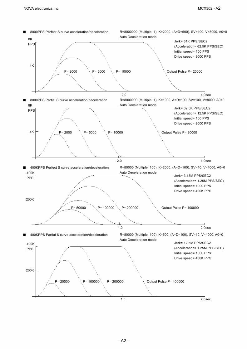
NOVA electronics Inc. MCX302 - A2
– A2 –
R=8000000 (Multiple: 1), K=2000, (A=D=500), SV=100, V=8000, A0=0Auto Deceleration mode
Jerk= 31K PPS/SEC2 (Acceleration= 62.5K PPS/SEC)Initial speed= 100 PPS Drive speed= 8000 PPS
8000PPS Perfect S curve acceleration/deceleration
2.0 4.0sec
4K
8K PPS
Output Pulse P= 20000 P= 10000P= 5000P= 2000
R=8000000 (Multiple: 1), K=1000, A=D=100, SV=100, V=8000, A0=0Auto Deceleration mode
Jerk= 62.5K PPS/SEC2 (Acceleration= 12.5K PPS/SEC)Initial speed= 100 PPS Drive speed= 8000 PPS
8000PPS Partial S curve acceleration/deceleration
2.0 4.0sec
4K
8K PPS
Output Pulse P= 20000 P= 10000P= 5000 P= 2000
R=80000 (Multiple: 100), K=2000, (A=D=100), SV=10, V=4000, A0=0Auto Deceleration mode
Jerk= 3.13M PPS/SEC2 (Acceleration= 1.25M PPS/SEC)Initial speed= 1000 PPS Drive speed= 400K PPS
400KPPS Perfect S curve acceleration/deceleration
1.0 2.0sec
200K
400K PPS
Output Pulse P= 400000P= 200000P= 100000P= 50000
R=80000 (Multiple: 100), K=500, (A=D=100), SV=10, V=4000, A0=0 Auto Deceleration mode
Jerk= 12.5M PPS/SEC2 (Acceleration= 1.25M PPS/SEC)Initial speed= 1000 PPS Drive speed= 400K PPS
400KPPS Partial S curve acceleration/deceleration
1.0 2.0sec
200K
400K PPS
Output Pulse P= 400000P= 200000P= 100000 P= 20000

NOVA electronics Inc. MCX302 - A3
– A3 –
R=800000 (Multiple: 10), A=400, D=100, SV=50, V=4000, A0=0Acceleration = 500K PPS/SECDeceleration= 125K PPS/SECInitial Speed= 500PPS Drive Speed= 40K PPS
40KPPS Non-symmetrical Trapezoidal acceleration/deceleration
Output Pulse P= 30000P=20000 P=10000
P=5000
P=2000
1.2sec
40K
PPS
Acceleration = 125K PPS/SECDeceleration= 500K PPS/SECInitial Speed= 500PPS Drive Speed= 40K PPS
Individual acceleration/deceleration: WR3/D1=1,Triangle form prevention ON : WR3/D5=1
P= 30000P=20000 P=10000
P=5000
P=2000
1.2sec
40K
PPS
R=800000 (Multiple: 10), A=100, D=400, SV=50, V=4000, A0=0
R=800000 (Multiple: 10), A=400, D=40, SV=50, V=4000, A0=0Acceleration= 500K PPS/SECDeceleration= 50K PPS/SECInitial Speed= 500PPS Drive Speed= 40K PPS
Output Pulse P= 30000P=20000 P=10000 P=5000
1.6sec
40K
PPS
Acceleration = 50K PPS/SECDeceleration= 500K PPS/SECInitial Speed= 500PPS Drive Speed= 40K PPS
P= 30000P=20000 P=10000 P=5000
1.6sec
40K
PPS
R=800000 (Multiple: 10), A=40, D=400, SV=50, V=4000, A0=0

NOVA electronics Inc. MCX302 - B1
– B1 –
Appendix B Important notice
Ⅰ Notice for fixed pulse or continuous pulse driving in S-curve acceleration/deceleration
[Symptom]
When using fixed pulse driving or continuous pulse driving in S-curve acceleration/deceleration, driving is performed at an initial speed without acceleration.
[Occurrence Condition]
1. When fixed pulse driving or continuous pulse driving is performed in S-curve acceleration / deceleration mode
(WR3/D2=1), 2. the value of (Drive speed V - Initial speed SV) is lower than the half value of (V-SV) which is driven just before. 3. And in the driving just before, when ACC counter (which is used in S-curve acceleration / deceleration driving in
the IC) is not returned to 0 at the end of driving.
[Workaround]
Before start of driving, use following steps to workaround this behavior, with an inspection command to clear the internal ACC counter. This command is not described in the manual. When fixed pulse driving or continuous pulse driving is performed in S-curve acceleration/ deceleration mode (WR3/D2=1), write 44h command just before all the drive commands are written. (Example) Set mode for S-curve acceleration/deceleration Set Range (R) Set Jerk (K) Set Acceleration (A) Set Initial speed (SV) Set Drive speed (V) Set Output pulse number (P)
WR0 Axis assignment+44h ;Command for workaround
WR0 Axis assignment+20h ;Fixed pulse drive in the +direction
Waits for termination of driving
|
Set Output pulse number (P)
WR0 Axis assignment+44h ;Command for workaround
WR0 Axis assignment+21h ;Fixed pulse drive in the –direction

NOVA electronics Inc. MCX302 - B2
– B2 –
Waits for termination of driving
|
Change Drive speed (V)
WR0 Axis assignment+44h ;Command for workaround
WR0 Axis assignment+22h ;Continuous pulse drive in the +direction
Waits for termination of driving
Ⅱ Notice for Compare Register
[Symptom]
Although Range of Position Comparison between Position Counter and Compare Register(COMP+,-) is shown as -2,147,483,648 to +2,147,483,647 (signed 32-bit)on User’s Manual, actually it is -1,073,741,824 to +1,073,741,823(signed 31-bit)due to the defect of IC.
[Workaround]
Don’t compare the values over the range such as -1,073,741,824 to +1,073,741,823.

NOVA electronics Inc. MCX302 - B3
– B3 –
Ⅲ Notice for Fixed pulse driving in S-curve acceleration/deceleration
[Symptom]
When using fixed pulse driving in S-curve acceleration/deceleration, if one of the following occasions ① to ④ is taken just before finishing driving, pulse may be continuously outputted depending on setting value of parameters.
speed
time
drive speed
initial speed
one of ①~④ is excuted here. Figure 1. Speed profile of fixed pulse driving in S-curve acceleration/deceleration
① When decelerating stop command (26h) was given just before finishing driving ② When setting stop mode of hardware limit(nLMTP/M signal) as decelerating stop(WR2/D2=1), driving is
started and hardware limit of progress direction becomes active just before finishing driving ③ When software limit is enabled(WR2/D0,1=1), driving is started and hardware limit of progress direction
becomes active just before finishing driving ④ When nSTOP(2~0)signals are enabled(WR1/D5,3,1), fixed pulse driving is started and those signals become
active just before finishing driving ・ This trouble won’t happen when trapezoidal(liner) acceleration/deceleration drive or constant speed drive is
performed. ・ This trouble won’t be happened when continuous pulse driving in S-curve acceleration/deceleration. ・ This trouble won’t happen when any of Sudden stop command, EMGN signal, LMT signal of Sudden stop and
ALARM signal is outputted. Fixed pulse driving in S-curve acceleration/deceleration is performed as that driving speed and initial speed becomes equal and acceleration becomes zero(0) when driving finished ,which means all pulse outputted. But it’s impossible to make driving speed & initial speed equal and acceleration zero(0) in all combinations of parameters because of the problem of calculation accuracy. This trouble will happen if it is in the above mentioned occasion ①, ②, ③ or ④ as the factors of deceleration stop accidentally and driving speed hasn’t reached initial speed yet but acceleration has become zero(0) showing on Figure 2.
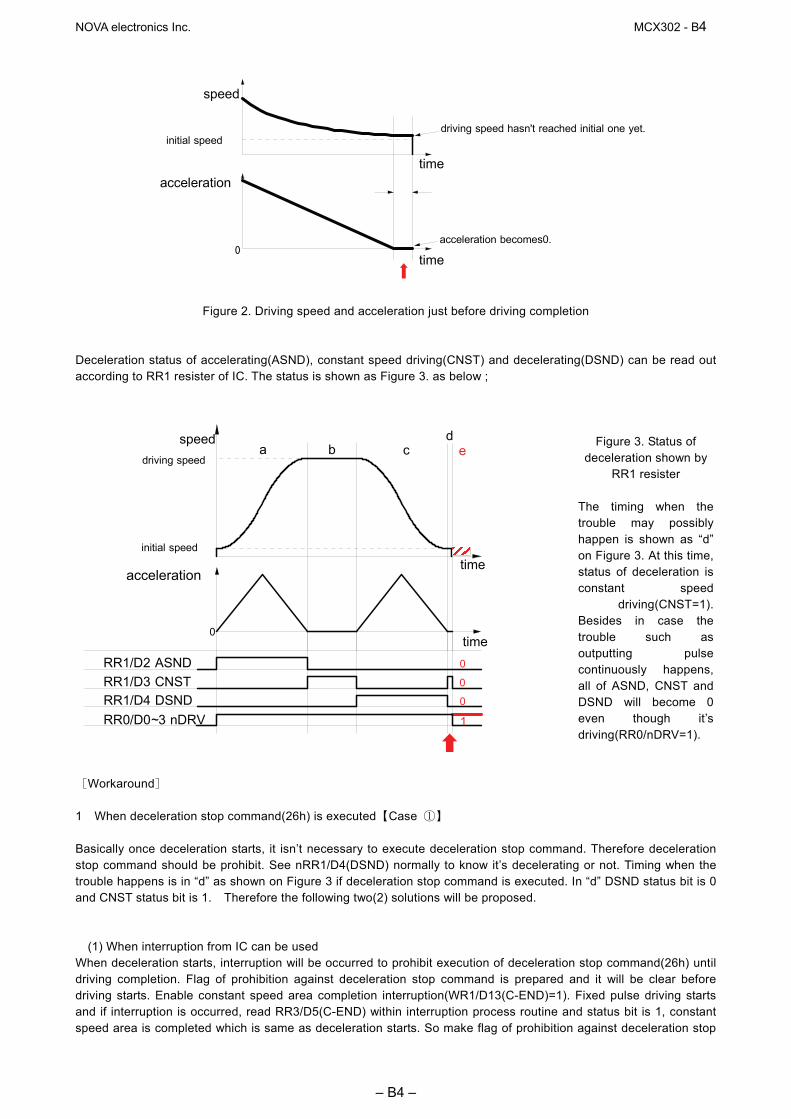
NOVA electronics Inc. MCX302 - B4
– B4 –
speed
time
time
initial speed
0
driving speed hasn't reached initial one yet.
acceleration becomes0.
acceleration
Figure 2. Driving speed and acceleration just before driving completion
Deceleration status of accelerating(ASND), constant speed driving(CNST) and decelerating(DSND) can be read out according to RR1 resister of IC. The status is shown as Figure 3. as below ;
Figure 3. Status of deceleration shown by
RR1 resister The timing when the trouble may possibly happen is shown as “d” on Figure 3. At this time, status of deceleration is constant speed
driving(CNST=1). Besides in case the trouble such as outputting pulse continuously happens, all of ASND, CNST and DSND will become 0 even though it’s driving(RR0/nDRV=1).
[Workaround] 1 When deceleration stop command(26h) is executed【Case ①】 Basically once deceleration starts, it isn’t necessary to execute deceleration stop command. Therefore deceleration stop command should be prohibit. See nRR1/D4(DSND) normally to know it’s decelerating or not. Timing when the trouble happens is in “d” as shown on Figure 3 if deceleration stop command is executed. In “d” DSND status bit is 0 and CNST status bit is 1. Therefore the following two(2) solutions will be proposed.
(1) When interruption from IC can be used When deceleration starts, interruption will be occurred to prohibit execution of deceleration stop command(26h) until driving completion. Flag of prohibition against deceleration stop command is prepared and it will be clear before driving starts. Enable constant speed area completion interruption(WR1/D13(C-END)=1). Fixed pulse driving starts and if interruption is occurred, read RR3/D5(C-END) within interruption process routine and status bit is 1, constant speed area is completed which is same as deceleration starts. So make flag of prohibition against deceleration stop
speed
timeacceleration
time
driving speed
initial speed
0
RR1/D2 ASNDRR1/D3 CNSTRR1/D4 DSNDRR0/D0~3 nDRV
a b cd
e
1
0
0
0
NOVA electronics Inc. MCX302 - B5
– B5 –
command 1. Besides it is possible that CNST(constant speed area) will occur just before driving completion. Then return WR1/D13 status bit from 1 to 0 in order to prevent interruption. On the other hand, within task, see flag and if it’s 1, don’t execute deceleration stop command.
(2) When interruption can’t be used Terms when deceleration stop command should be executed in accelerating and constant speed driving such as “a” and “b” on Figure 3. Status of deceleration for both “d” (timing when the trouble happens) and “b” (constant speed driving) is same as constant speed driving as shown on Figure 3. But there is difference of driving speed between two. Driving speed in “b” is near that of setting driving speed. Driving speed in “d” is near that of initial speed. Therefore before driving starts, prepare judgmental speed which is middle one between initial speed and setting speed ((Driving speed - initial speed)/2 + initial speed). When execute deceleration stop command during driving, make sure status is accelerating(ASND=1) or constant speed driving(CNST=1) and driving speed is same or faster than judgmental speed. 2 Hardware limit(nLMTP/M signal) at deceleration stop mode【Case ②】 Basically use hardware limit(nLMTP/M signal) at Sudden stop mode when fixed pulse driving in S-curve acceleration/deceleration. Out of necessity, when use hardware limit at deceleration stop mode, prepare the following measures. If multi-axes are controlled in the same time, (1) When interruption from IC can be used is effective. (1) When interruption from IC can be used Constant speed area (“b” area) on Figure 3 is set as occurrence factor of interruption. But this interruption is also happened when there is “d” area just before driving stops on Figure 3 such as when driving speed reaches initial speed or when acceleration becomes 0(zero). There should occur “d” area definitely if the trouble is happened just before driving stops, driving speed hasn’t reached initial speed yet, acceleration becomes 0 and decelerating stop requirement is executed. The measure is to judge if the trouble happens or not in the timing of interruption when “d” area ends. Make constant speed area finishing interruption of IC active(WR1/D13(C-END)=1). Start fixed pulse driving in S-curve acceleration/deceleration and when interruption is happened, interruption processing is executed as follows;
NOVA electronics Inc. MCX302 - B6
– B6 –
INTERRUPTION PROCESSING
nRR3/D5(C-END)=1?
nRR1/D4(DSND)=1?
RR0/D0(X AXIS)=0?
nRR1/D12orD13=1?
nRR1/D2=D3=D4=0?
SUDDEN STOP COMMAND(27h)
PROCESSING FINISHED
① GOES OUT CONSTANT SPEED AREA?
② DECELERATING AREA?
③ DRIVING FINISHES?
④ FORWARD LIMIT IS ON?
⑤ ASND=CNST=DSND=0?
⑥ JUDGED AS TROUBLE HAPPENS
This shows the interruption when driving goes into decelerating area (c) from constant speed area (b) is normal. Make driving finished as it goes.
This shows the interruption when driving has finished normally in area (d). Make driving finished as it goes.
During driving, backward limit never be on. So RR1/D12, D13 won’t be 1 due to backward limit.
no OTHER INTERRUPTION FACTORS
no
no
no
no
yes
yes
yes
yes
① Check if driving goes out constant speed area or not. If RR3/D5(C-END) bit of driving axis is 0, there are other
interruption factors. Execute those interruption processing. ② Check if driving goes into decelerating area or not. If it’s RR1/D4(DSND)=1, make it finished as it goes because
driving goes into “c” area from “b” area on Figure 3. If it’s RR1/D4(DSND)=0, move it to ③ processing because driving has gone out “d” area.
③ Check if driving has finished or not. If it’s finished, make it finished as it goes because driving has finished normally. But if it’s not finished yet, surely trouble have happened because status is shown as it’s still driving even though driving has gone out “d” area.
④ Check if hard limit is ON or OFF. Since RR1/D12 bit becomes 1 if + limit is ON and RR1/D13 bit becomes 1 if – limit is ON, if it’s D12=1 or D13=1, judge forward limit is ON.
⑤ If trouble has happened, it becomes ASND=CNST=DSND=0. Check them all. ⑥ Execute sudden stop command(27h).

NOVA electronics Inc. MCX302 - B7
– B7 –
(2) When interruption can’t be used In “d” area on Figure 3, if forward limit is active, the trouble will happen, more exactly saying, it will seldom happen. There isn’t any method to avoid it before it happens. So immediately after the trouble happens, take means to stop driving. If the trouble happens (“e” area on Figure 3), status keeps driving(RR0/nDRV=1), status of acceleration/deceleration is 0 in ASND, CNST, DSND. This is completely abnormal state. So the example of measure is shown as follows;
DRIVING STARTS
KEEP DRIVING?
FORWARD LIMIT ON?
KEEP DRIVING?
ASND=CNST=DSND=0?
SUDDEN STOP COMMAND(27h)
KEEP DRIVING?
DRIVING COMPLETION
RR0/DRV bit
RR1/D12,13
RR1/ASND,CNST,DSND bit
no
no
no
no
no
yes
yes
yes
yes
yes
When start fixed pulse driving in S-curve acceleration/deceleration, always read out status of progress directional hardware limit(RR1/D12,D13) with timer interruption. If limit signal becomes active, read out bit status of ASND(D2), CNST(D3) and DSND(D4) in RR1 resister and execute Sudden stop command(27h) one time only if all those 3 bits are 0. 3 Software limit【Case ③】 In fixed pulse driving, the target position(goal) can be calculated from present position(logical position counter value) and number of output pulse. If target position is over value of software limit, don’t drive to avoid the trouble.

NOVA electronics Inc. MCX302 - B8
– B8 –
4 Deceleration stop with STOP(2~0) Signal【Case ④】 Normally deceleration stop with STOP(2~0)signal is performed during continuous pulse driving. But out of necessity, when deceleration stop with STOP(IN) signal is performed during fixed pulse driving in S-curve deceleration, there isn’t any method to avoid it before the trouble happens like chapter 2.2. So the example of measure is shown as follows;
DRIVING STARTS
KEEP DRIVING?
IS STOP SIGNAL ACTIVE?
KEEP DRIVING?
ASND=CNST=DSND=0?
SUDDEN STOP COMMAND(27h)
KEEP DRIVING?
DRIVING COMPLETION
RR0/DRV bit
See RR1/D8~11
RR1/ASND,CNST,DSND bit
no
no
no
no
no
yes
yes
yes
yes
yes
If you need more assistance, please e-mail us at [email protected].


![Liste des données - Home - Yamaha - United States · · 2018-04-19Setting the octave [Octave] *1 65 Setting the volume level [Volume] *1 65 Setting the position of the right and](https://img.pdfslide.net/doc/110x75/5ae288eb7f8b9ae74a8c98f4/liste-des-donnes-home-yamaha-united-states-the-octave-octave-1-65-setting.jpg)