Embed Size (px)
Citation preview
19
Coarse Grained Reconfigurable Architectures Chapter 2
2. Coarse Grained Reconfigurable Architectures
While the first systems for reconfigurable computation featured fine grainedFPGAs, it was soon discovered, that FPGAs bear different disadvantages forcomputational tasks. First, due to the bit-level operations, operators for widedatapaths have to be composed of several (bit-level) processing units. Thisincludes typically a large routing overhead for the interconnect between theseunits and leads to a low silicon area efficiency of FPGA computing solutions.Also, the switched routing wires use up more power than hardwired connections.
A second drawback of the fine granularity is the high volume of configurationdata needed for the large number of both processing units and routing switches.This implies the need for a large configuration memory, with an according powerdissipation. The long configuration time, which is implied by this problem,makes execution models relying on a steady change of the configurationimpossible.
As a third disadvantage, application development for FPGAs is very similar toVLSI design due to the programmability at logic level. The mapping ofapplications from common high-level languages is difficult compared to thecompilation onto a standard microprocessor, as the granularity of the targetFPGA does not match that of the operations in the source code. The standard wayof application specification is still a hardware description language, whichrequires a hardware expert. In the following design process, the large number ofprocessing units leads to a complex synthesis, which uses up much computationtime.
Coarse grained reconfigurable architectures try to overcome the disadvantages ofFPGA-based computing solutions by providing multiple-bit wide datapaths andcomplex operators instead of bit-level configurability. In contrast to FPGAs, thewide datapath allows the efficient implementation of complex operators insilicon. Thus, the routing overhead generated by having to compose complexoperators from bit-level processing units is avoided.
Regarding the interconnects between processing elements, coarse grainarchitectures also differ in several ways to FPGAs. The connections are multiplebits wide, which implies a higher area usage for a single line. On the other hand,the number of processing elements is typically several orders of magnitude lowerthan in an FPGA. Thus, much fewer lines are needed, resulting in a globally lowerarea usage for routing. The lower number and higher granularity of
Chapter 2 Coarse Grained Reconfigurable Architectures
20
communication lines allows also for communication resources, which would bequite inefficient for fine grained architectures. Examples for such resources aretime-multiplexed buses or global buses, which connect every processing element.
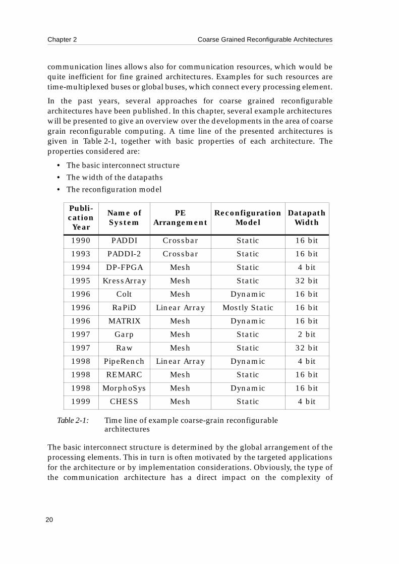
In the past years, several approaches for coarse grained reconfigurablearchitectures have been published. In this chapter, several example architectureswill be presented to give an overview over the developments in the area of coarsegrain reconfigurable computing. A time line of the presented architectures isgiven in Table 2-1, together with basic properties of each architecture. Theproperties considered are:
• The basic interconnect structure• The width of the datapaths• The reconfiguration model
The basic interconnect structure is determined by the global arrangement of theprocessing elements. This in turn is often motivated by the targeted applicationsfor the architecture or by implementation considerations. Obviously, the type ofthe communication architecture has a direct impact on the complexity of
Publi-cation Year
Name of System
PEArrangement
Reconfiguration Model
Datapath Width
1990 PADDI Crossbar Static 16 bit
1993 PADDI-2 Crossbar Static 16 bit
1994 DP-FPGA Mesh Static 4 bit
1995 KressArray Mesh Static 32 bit
1996 Colt Mesh Dynamic 16 bit
1996 RaPiD Linear Array Mostly Static 16 bit
1996 MATRIX Mesh Dynamic 16 bit
1997 Garp Mesh Static 2 bit
1997 Raw Mesh Static 32 bit
1998 PipeRench Linear Array Dynamic 4 bit
1998 REMARC Mesh Static 16 bit
1998 MorphoSys Mesh Dynamic 16 bit
1999 CHESS Mesh Static 4 bit
Table 2-1: Time line of example coarse-grain reconfigurable architectures
21
Coarse Grained Reconfigurable Architectures Chapter 2
application mapping. The predominating structure of the architectures presentedhere is a two-dimensional mesh. In other architectures, the processing elementsare arranged in one or more linear arrays. The third interconnect structure foundis a crossbar switch being used to connect processing elements. This allowsbasically arbitrary connections.
The width of the datapath ranges from two bits to 32 bits. The selection of thedatapath width for an architecture is a trade-off between flexibility and efficiency.While a wide datapath allows an efficient implementation of the processingelement for operations on a whole data word, the execution of operations on partsof a data word, which occur in certain applications, requires typically severalexecution steps, including the extraction of the relevant bit range. A smallerdatapath allows the direct execution of such operations or implies less extractionoverhead. On the other hand, operators for wider data words have to becomposed of several processing elements, which inflicts routing overhead.
The reconfiguration model determines, when a new configuration is loaded intothe architecture. For architectures featuring static reconfiguration, aconfiguration is loaded at the beginning of the execution and stays during thecomputation phase. When a new configuration has to be loaded, the executionmust stop. The dynamic reconfiguration model allows a new configuration to beloaded while the application is running. This includes the case, that the executionrelies on steady reconfiguration of the processing elements. Some architecturesuse normally static reconfiguration, but allow dynamic reconfiguration forspecial purposes like the configuration of unused parts for the next task, while acomputation is running. Such architectures are denoted as static, as this remainsthe main reconfiguration model.
The presentation of the example systems is ordered by the interconnect structure.In the next subsection, nine mesh-based architectures are described. Then, twosystems based on linear arrays are presented, and finally, two systems employinga crossbar switch are shown.
2.1 Mesh-Based ArchitecturesMesh-based architectures arrange their processing elements in a rectangulararray, featuring horizontal and vertical connections. This structure allowsefficient parallelism and a good use of communication resources. However, theadvantages of a mesh are traded for the need of an efficient placement androuting step. The quality of this step can have a remarkable impact on theapplication performance. Though, due to the relative low number of processingelements, the placement and routing is often much less complex than for e.g.FPGAs.
Chapter 2 Coarse Grained Reconfigurable Architectures
22
The arrangement of the processing elements encourages nearest neighbor linksbetween adjacent elements as an obvious communication resource. Typically,longer lines are added with different lengths, which allow connections overseveral processing elements.
The first architecture called DP-FPGA [ChLe94] was published by D. Cherepachaand D. Lewis from the University of Toronto. This approach shows clearly itsrelation to FPGAs, featuring bit-sliced ALUs and a routing architecture quitesimilar to its fine-grained ancestors. The KressArray-I [Kres96] by R. Kress ofUniversity of Kaiserslautern is an approach with a very wide datapath, whichrequired to reduce the communication resources in order to achieve a feasiblechip design. However, the KressArray features also a serial bus as a high-levelconnection, which connecs all processing elements, and is globally scheduled.The KressArray-I was accompanied by a control unit and integrated into theXputer prototype MoM-3 [Rein99]. The Colt [BAM96] architecture by R. Bittner,P. Athanas and M. Musgrove from Virginia State University features a singleinteger multiplier in addition to the mesh of processing elements. Thisarchitecture is a study for the wormhole runtime-reconfiguration computingparadigm, which relies on heavy dynamic reconfiguration. The MATRIX[MiDe96] system by E. Mirsky and A. DeHon of MIT is the first one to extend theprocessing elements to small processors, featuring local instruction memories ineach element as well as small data memories. While the previous systemsresembled stand-alone architectures (sometimes accompanied by a control unit),the Garp [HaWa97] architecture by J. Hauser and J. Wawrzynek from Universityof Berkeley is a system composed of a normal microprocessor with areconfigurable coprocessor. It features lookup-table based processing elementswith only two-bit wide datapaths. In fact, this architecture comes very close to anFPGA and is often considered to be fine-grained. It appears in this chapter, as thebasic unit of reconfiguration is a whole row of processing elements, which forma kind of reconfigurable ALU. Though, the available routing resources of thisapproach classify it as a mesh-based architecture. The Raw machine paradigm[WTSS97], which has been developed by E. Waingold et al. from MIT features themost complex processing elements with a complete RISC processor, data andinstruction memory, and a programmable switch for time-multiplexed nearestneighbor interconnects. In contrast to other approaches, which try to provide amore complex FPGA, this architecture tries to realize a mesh of less complexmicroprocessors, with the main responsibility for proper execution moved to thesoftware environment at compile time. The REMARC [MiOl98a] architecture byT. Miyamori and K. Olukotun from Stanford University is another co-processor,consisting of 64 small processors with memory. The MorphoSys [LSLB99]machine by G. Lu et al. from Irvine University is also a hybrid system consistingof a RISC processor with a reconfigurable coprocessor. Here, the reconfigurablemesh is accompanied by a frame buffer for intermediate data. The last

23
Coarse Grained Reconfigurable Architectures Chapter 2
architecture shown is the CHESS [MVS99] array by A. Marshall et al. fromHewlett Packard Laboratories. This architecture features a unique PEarrangement in the form of a chess board, with embedded memories to supportmultimedia applications.
2.1.1 The Datapath FPGAIn 1994, Cherepacha and Lewis introduced the DP-FPGA (Datapath FPGA)[ChLe94], [ChLe96]. The DP-FPGA is intended for implementing regularlystructured datapaths like the ones found in digital signal processing,communications, circuit emulation and special-purpose processor applications.The system comprises three basic components: A control logic, the datapath andmemory. The control logic resembles a general purpose architecture adequate forimplementing random logic. The memory is useful for large datapath designs.The datapath, which also occupies the most area of the design, is unique for theDP-FPGA and will be described in more detail in the following.
The targeted applications for the DP-FPGA may contain several datapaths ofvarious widths, where also a small number of irregularities in some bit-slices isallowed. To provide both flexibility like bit-level devices and area advantages likeALU level architectures, the DP-FPGA features a medium granularity of four bitsfor both logic and routing resources. Thus, the basic logic block is made of fourbit-slices, which are programmed identically using the same set of configurationbits. Each bit-slice comprises a lookup table, a carry chain and a four-bit register,the latter inspired by an experimental study by Rose et al [RFLC90].
An overview on the routing architecture of the DP-FPGA is shown in figure 2-1.In contrast to other architectures, the DP-FPGA features separate routingresources for data (horizontal) and control signals (vertical), both using four-bitbuses. Vertical data routing is needed for shifts of multiples of four bits,connections to the I/O pads and connections spanning several rows, when theentire bit-slice does not fit in one row. However, such vertical routing connectionsare only possible in a limited way by using control wires for data transport.
To enable bit-granular shifts and irregularities in datapaths in spite of the four-bitgranularity, shift blocks are included in the architecture, which can perform upand down shifts from zero to three bits. As these shifters can access data lines aswell as control lines for source and destination, limited vertical data routing isalso possible.
2.1.2 The KressArray-IIn 1995, the KressArray-I [Kres96] was introduced under the name rDPA(reconfigurable DataPath Architecture). The architecture was originally targetedas a reconfigurable ALU (rALU) for the MoM-3 prototype [Rein99] of the Xputer
Chapter 2 Coarse Grained Reconfigurable Architectures
24
machine paradigm [HHW90], [HHRS91], [Hirs91], [AHRS94]. As Xputers arebased on a strict separation of control path and datapath, the KressArray-I wasused exclusively for application datapaths, which can include branches as well aswhile and do-while loops. Although the KressArray-I is dynamically partiallyconfigurable, the typical datapath would not change during execution.
The general structure of the KressArray-I system is depicted in figure 2-2. Itconsists of the array itself, resembling a mesh of processing elements calledrDPUs (reconfigurable DataPath Units) and a controller unit. The controllermanages the input and output of data streams to and from the array as well as theconfiguration process. For data I/O, the controller interfaces between the arrayand an external bus to the memory. Data streams are provided over this bus,controlled by the MoM-3 machine. For synchronization of input and output datastreams, a data buffer register is provided. Further, the status of the array, like thefinishing of the computation, is signaled by a status generation unit. The datawords of the I/O streams may have to be distributed to arbitrary rDPUs. For thispurpose, every rDPU can be addressed individually. An address generation unitdelivers the correct addresses for the rDPU registers, so the data can be written tothe correct location. For intermediate results of the computation, a register filewith 64 entries of 34 bits each is integrated, which can also be used as a smartcache to save memory cycles. The global control of all the parts is done by theKressArray-I control unit, which executes a control program. The instruction setincludes operations for data transfer between the external bus, the register file,and specific rDPUs in the array. The control program is loaded during theconfiguration time by the configuration unit, which manages also the
L sh
CD
CC
SD
Sc
L sh
CD
CC
SD
Sc
L sh
CD
CC
SD
Sc
L sh
CD
CC
SD
Sc
shift chain4-bit data bus1-bit control wirecarry chainL: logic blocksh: shift blockCC: control connection blockCD: data connection blockSC: control switch blockSD: data switch block
Figure 2-1: The DP-FPGA architecture
25
Coarse Grained Reconfigurable Architectures Chapter 2
configuration of the rDPU array. The controller is connected to the rDPU array bya serial global bus leading to every single rDPU, which is used for data transfersand for configuration.
The KressArray-I itself resembles a rectangular array of rDPUs. In the prototypeimplementation, a subarray of three by three rDPUs was implemented on onechip. The whole array was composed of two by four chips, resulting in an arrayof six by twelve (72) rDPUs. Each single rDPU contains an ALU with a datapathof 32 bits wide, featuring all integer operators of the C programming language.The operators are microprogrammed, so the operator repertory can be extendedif necessary. The KressArray architectures are based on transport-triggeredexecution. That means, an operator starts its computation as soon as all inputoperands are available.
The routing architecture of the KressArray-I features nearest neighborconnections from each rDPU to its southern and eastern neighbors. As anadditional routing resource for longer connections, the serial global bus isavailable, which is also used for data I/O and the transfer of intermediate resultsbetween the array and the register file in the controller. This global bus iscontrolled by a static schedule, which is determined at compile-time. The rALUcontroller uses this schedule to manage the data transfers over the global bus.
Register
File
KressArray-I Address
Generation
KressArray-I control unit
external Bus to Host and Main Memory (MoM Bus )
KressArray-Iglobal I/O bus
op op op op op op
op op op op op op
op op op op op op
Unit
status FIFO
conf.unit
rALU controller
op op op op op op
reconf. datapath unit (rDPU)
Figure 2-2: KressArray-I architecture
Chapter 2 Coarse Grained Reconfigurable Architectures
26
2.1.3 The Colt SystemThe Colt system [BAM96], [BiAt97], presented in 1996 by Bittner, Athanas andMusgrove, combines concepts from FPGAs and data flow computing. Colt ismainly targeted for DSP applications, which are implemented by configuringpipelines or parts of pipelines onto the architecture. These pipelines are then usedto process data streams. Thus, the Colt architecture can be seen as a Pipenet asdiscussed by Hwang [Hwan93]. The granularity of the data paths for routing andoperations is 16 bits, with only limited possibilities for finer-grained operations.The Colt architecture relies highly on runtime reconfiguration (RTR). It usesWormhole-RTR as an execution model. Hereby, the data streams to be processedcarry a header with configuration information. This header holds theconfiguration data for both the routing and the functionality of all processingelements the data stream encounters on its way. Thus, the model employs thewormhole routing method known from computing networks [DaSe87].
The general structure of the Colt architecture is shown in figure 2-3. The maincomponents are a mesh of IFUs (Interconnected Functional Units), a crossbarswitch, an integer multiplier, and six data ports. The mesh of IFUs is the maincomputational facility. Each IFU features a 16-bit ALU with all logical operationswith two inputs as well as a carry chain for add, subtract and negation.Furthermore, each IFU contains a barrel shifter to support multipliers andfloating point arithmetic, a conditional unit for data-dependent flow control, andoptional delay units for synchronization of pipelines. In addition to the ALUoutput, there is an auxiliary output passing through one of the inputs to supportfloating point arithmetic. Thus, the core of an IFU has two inputs and twooutputs. The IFUs are connected by unidirectional nearest neighbor links in eachdirection with one outgoing and one incoming port at each side of the IFU.Additionally, each row and column features a so-called skip bus, which is asegmented bus featuring bidirectional local links, which can be merged. The IFUsin the northern and southern rows of the mesh differ from the inner IFUs inregard of their links at the edge, which are connected to the crossbar. In thenorthern row, each IFU has two inputs at the north side coming from the crossbar,while in the southern row, each IFU features a single output at the south sidegoing to the crossbar. At the eastern and western edge, the two nearest neighborlinks and the skip bus are connected to the opposing edge, thus forming a torusstructure. The dedicated integer multiplier has two 16 bit inputs and two 16 bitoutputs for the high and low word of the 32 bit result. The six data ports arebidirectional, each 20 bits wide with 16 bits for data and four bits for stream flowcontrol. The crossbar is used to make nearly arbitrary connections between themesh, the multiplier and the data ports.
27
Coarse Grained Reconfigurable Architectures Chapter 2
2.1.4 The MATRIX architectureThe MATRIX architecture by Mirsky and DeHon [MiDe96], [Mirs96], [Mirs97]was introduced in 1996. It is aimed at general computing. The main idea is tomake the amount of the basic resources of a computing system, namelycomputational units, instruction storage and data memory, adaptable toapplication requirements. Although the reconfiguration is meant to happen at aper task basis, the processing elements can be programmed using instructionstorage to change their behavior and data sources on a cycle-by-cycle basis.
The MATRIX comprises an array of identical Basic Functional Units (BFUs). EachBFU contains an 8-bit ALU, a 256 words of 8-bit memory and a control logic. TheALU features the standard set of arithmetic and logic functions and a multiplier.A configurable carry-chain between adjacent ALUs can be used to cascade ALUsfor wide-word operations. The control logic can generate local control signals byseveral ways. A pattern matcher can be used to generate control signals from theALU output data. A reduction network can be employed for control generatedfrom neighbor data. Finally, a 20-input, 8-output NOR block may be used as halfof an PLA to produce control signals. According to these features, a BFU can serveas an instruction memory, a data memory, a register-file-ALU combination, or anindependent ALU function. Due to the routing resources of the MATRIX,instructions may be routed over the array to several ALUs. Thus, a highcompression rate for instructions can be achieved.
Multiplier
DP
DP
DP
SmartCrossbar
IFUIFUIFUIFU
IFUIFUIFUIFU
IFUIFUIFUIFU
IFUIFUIFUIFU
DP
DP
DPI/O Pins
I/O Pins
I/O Pins
I/O Pins
I/O Pins
I/O Pins
Figure 2-3: General structure of the Colt architecture
IFU: InterconnectedFunctional Unit
DP: Data Port
Chapter 2 Coarse Grained Reconfigurable Architectures
28
The routing architecture of the MATRIX, which is sketched in figur e2-4, consistsof a hierarchical network with three levels, each consisting of 8-bit buses. Thelevels are nearest neighbor connections, length four bypass connections, andglobal lines. The nearest neighbor connections link each BFU to all of itsneighbors within manhattan distance two (see left side of figure 2-4). The lengthfour bypass connections (right side of figure 2-4) allows corner turns, local fan-out, medium distance interconnect, and some data shifting and retiming. Theglobal lines span an entire row or column. There are four of them in every rowand column.
2.1.5 The Garp ArchitectureThe Garp architecture concept [HaWa97] first published in 1997 by Hauser andWawrzynek, consists of a standard Processor accompanied by a reconfigurablearchitecture, aiming to combine the advantages of both concepts. By including amicroprocessor, the Garp is targeted for ordinary processing environments, withthe reconfigurable array being only activated for acceleration of specific loops orsubroutines. Although the processing elements of Garp resemble basically LUTswith a two bit datapath, the architecture is considered to be medium-grained, asthe basic unit of reconfiguration is a cluster of several processing elements.
Figure 2-4: Local interconnect and length four bypass interconnect of the MATRIX architecturea) Nearest neighbor interconnect within distance twob) Length four bypass interconnect
a) b)
29
Coarse Grained Reconfigurable Architectures Chapter 2
Garp consists of a main processor resembling a MIPS-II attached to areconfigurable array. The instruction set of the processor has been extended withinstructions to configure and control the array. An execution of the reconfigurablearray is initialized by the processor specifying the number of clock cycles thecomputation in the array should last. Hereby, the processor clock and the arrayclock do not need to be the same.
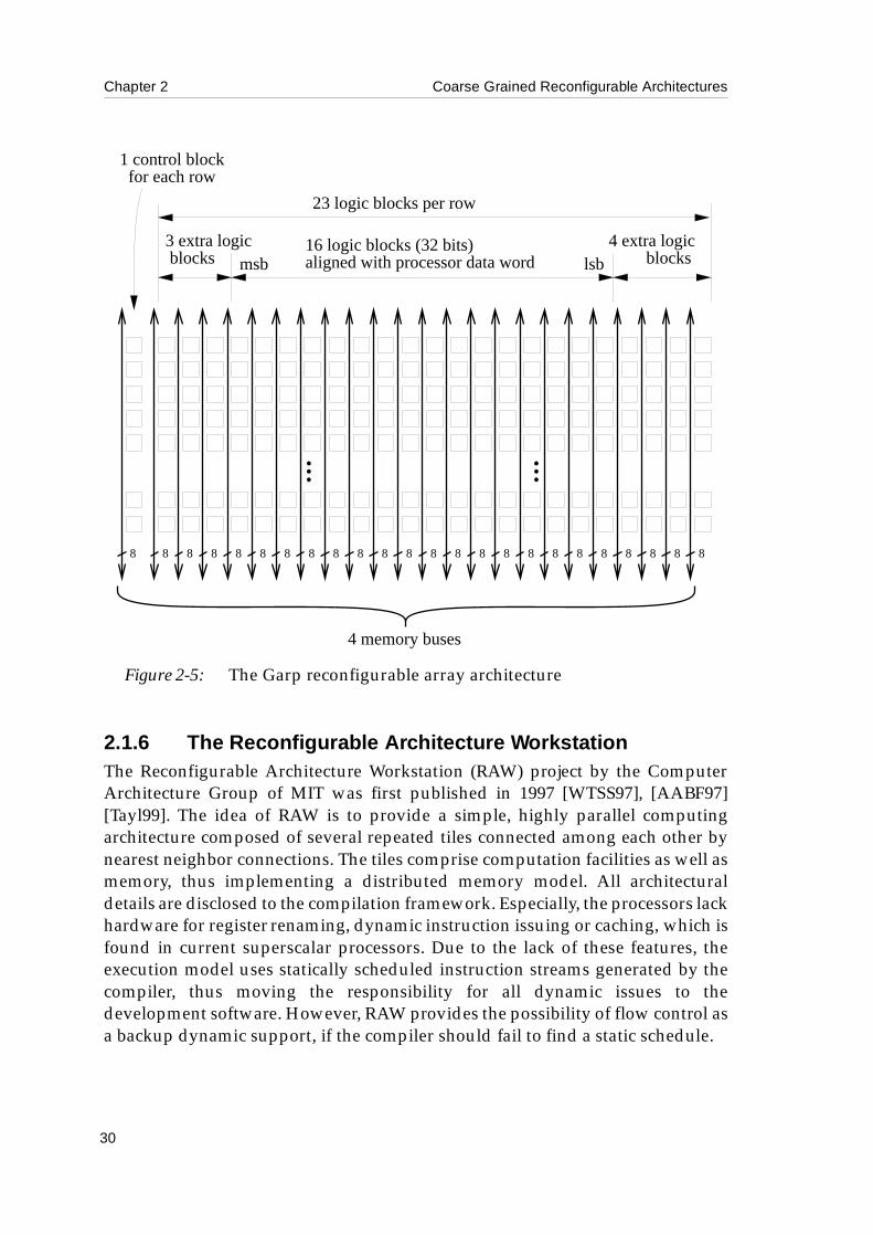
The reconfigurable array consists of at least 32 rows of processing elements(called blocks) arranged in 24 columns. An overview of this structure is given infigure 2-5. The array is connected to the processor by vertical buses, with four 2bit buses in each column. These buses are used for data I/O between the arrayand the memory or the processor. Memory accesses can be initiated by thereconfigurable array, but the data connection to memory is restricted to thecentral 16 columns. However, the array can access the same memory hierarchy asthe main processor. The blocks in the leftmost column are dedicated controlblocks, which are used for interfacing tasks like interrupting the processor orinitiating the mentioned memory accesses. The basic unit of reconfiguration isone row, which can be seen to as a kind of reconfigurable ALU, being formedfrom relatively fine-grained blocks. To allow fast switching of configurations, thearray also features a distributed cache with depth four, which stores the leastrecently used configurations. Although the array is partially reconfigurable, therecan be only one active configuration at a time.
Each block in the reconfigurable array features a datapath of 2 bits width and canimplement a function of up to four 2 bit inputs and two outputs. Wider datapathscan be formed by joining blocks in the same row. A carry chain is provided tosupport the build of wide adders, shifters or similar functions. The blockscomprise two-bit lookup tables with three inputs to implement the functions aswell as two clocked registers. Three of the four inputs are fed into the lookup-tables, forming one output value, while the second output is a direct copy of thefourth input. The two outputs can be sent to three different paths leading to otherblocks.
The routing architecture of the reconfigurable array consists of horizontal andvertical lines of different length. Conforming to the datapath of the blocks, theselines are 2 bits wide. Unlike other architectures, the horizontal and vertical linesare not segmented the same way, but are arranged in different patterns, beingoptimized for different purposes. Several short horizontal lines with segmentsspanning 11 blocks are provided to support multi-bit shifts along a row, whilevertical wires with different segment lengths are used for connecting functionalunits laid out horizontally. In addition to this, some long horizontal lines span thewhole array to enable the broadcast of control signals to the blocks of a singlemulti-bit operation.
Chapter 2 Coarse Grained Reconfigurable Architectures
30
2.1.6 The Reconfigurable Architecture WorkstationThe Reconfigurable Architecture Workstation (RAW) project by the ComputerArchitecture Group of MIT was first published in 1997 [WTSS97], [AABF97][Tayl99]. The idea of RAW is to provide a simple, highly parallel computingarchitecture composed of several repeated tiles connected among each other bynearest neighbor connections. The tiles comprise computation facilities as well asmemory, thus implementing a distributed memory model. All architecturaldetails are disclosed to the compilation framework. Especially, the processors lackhardware for register renaming, dynamic instruction issuing or caching, which isfound in current superscalar processors. Due to the lack of these features, theexecution model uses statically scheduled instruction streams generated by thecompiler, thus moving the responsibility for all dynamic issues to thedevelopment software. However, RAW provides the possibility of flow control asa backup dynamic support, if the compiler should fail to find a static schedule.
lsb16 logic blocks (32 bits)aligned with processor data word
3 extra logic blocks
23 logic blocks per row
msb
1 control block for each row
88 88 88 88 88 88 88 88 88 88 8888
blocks 4 extra logic
4 memory buses
Figure 2-5: The Garp reconfigurable array architecture
31
Coarse Grained Reconfigurable Architectures Chapter 2
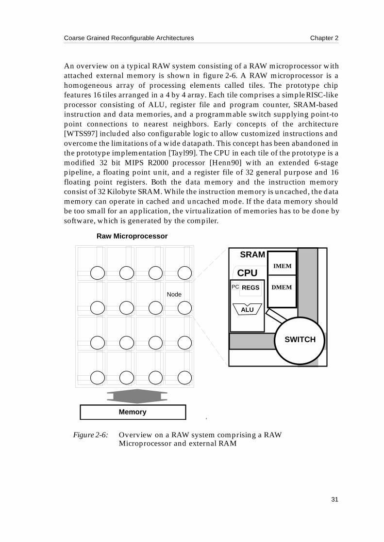
An overview on a typical RAW system consisting of a RAW microprocessor withattached external memory is shown in figure 2-6. A RAW microprocessor is ahomogeneous array of processing elements called tiles. The prototype chipfeatures 16 tiles arranged in a 4 by 4 array. Each tile comprises a simple RISC-likeprocessor consisting of ALU, register file and program counter, SRAM-basedinstruction and data memories, and a programmable switch supplying point-topoint connections to nearest neighbors. Early concepts of the architecture[WTSS97] included also configurable logic to allow customized instructions andovercome the limitations of a wide datapath. This concept has been abandoned inthe prototype implementation [Tayl99]. The CPU in each tile of the prototype is amodified 32 bit MIPS R2000 processor [Henn90] with an extended 6-stagepipeline, a floating point unit, and a register file of 32 general purpose and 16floating point registers. Both the data memory and the instruction memoryconsist of 32 Kilobyte SRAM. While the instruction memory is uncached, the datamemory can operate in cached and uncached mode. If the data memory shouldbe too small for an application, the virtualization of memories has to be done bysoftware, which is generated by the compiler.
Figure 2-6: Overview on a RAW system comprising a RAW Microprocessor and external RAM
REGS
ALU
SWITCH
PC
SRAM
CPUIMEM
DMEMNode
Memory
Raw Microprocessor
Chapter 2 Coarse Grained Reconfigurable Architectures
32
The interconnect of the RAW architecture is done over nearest neighborconnections being optimized for single data word transfer. Communicationbetween tiles is pipelined over these connections and appears at register levelbetween processors, making it different from multiprocessor systems. Aprogrammable switch on each tile connects the four nearest neighbor links toeach other and to the processor.
The RAW architecture provides both a static and a dynamic network, which aremultiplexed on the physical structure described above. The static network isrealized by a dedicated processor in the switch, which controls data transfers. Thecompiler has to generate code for this switch processor based on a static schedulefor the data transfers. Thus, in the static network each data transfer is exactlydetermined at compile-time. For cases where a static schedule is not possible, adynamic network is provided, which can perform data transfers in free cycles notused by the static network. This network uses wormhole routing for the dataforwarding, with the routing information contained in a header put before thedata to be transmitted.
2.1.7 The Reconfigurable Multimedia Array CoprocessorThe Reconfigurable Multimedia Array Coprocessor (REMARC) [MiOl98a],[MiOl98b] by Miyamori and Olukotun was introduced in 1998. The architectureis a reconfigurable coprocessor aimed at multimedia applications like videocompression, video decompression, and image processing. The REMARC istightly coupled to a MIPS-II ISA [Kane88] RISC processor, which suppliessupport for coprocessors. The processor has been extended by specialinstructions to access the REMARC architecture in the same way as a floating-point coprocessor is accessed.
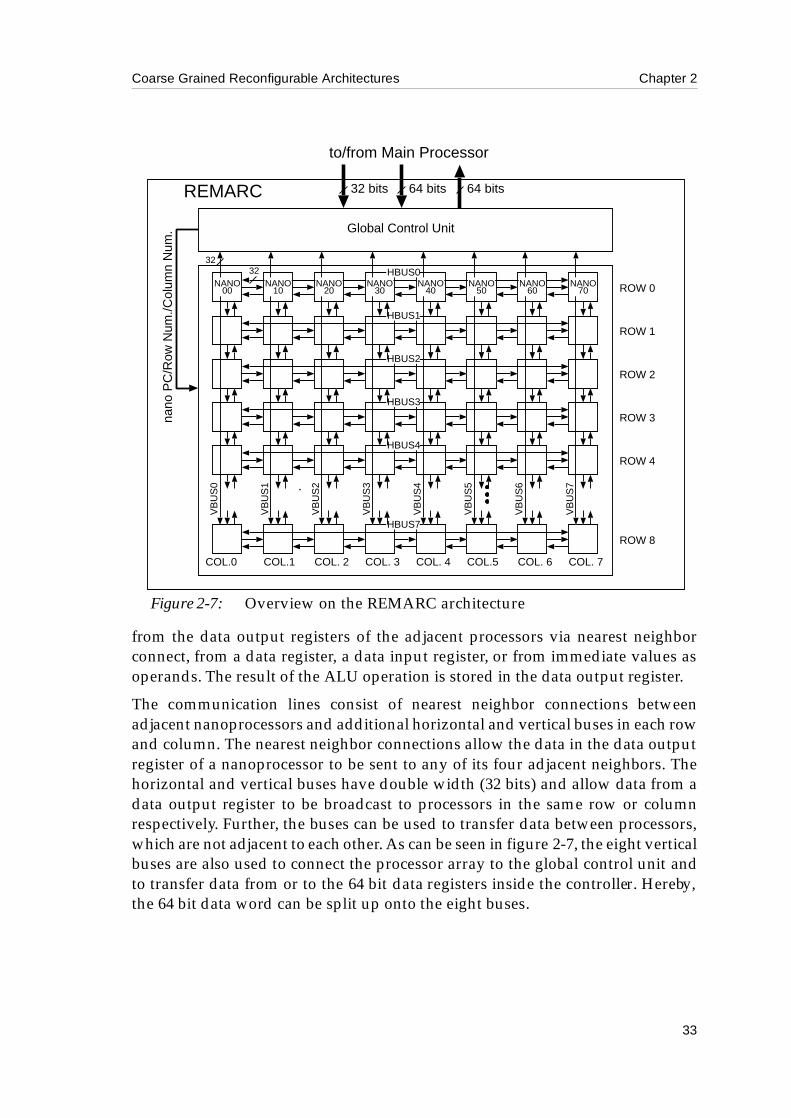
An overview on the REMARC architecture is given in figure 2-7. The REMARCconsists of an 8 by 8 array of processing elements (also called nanoprocessors),which is attached to a global control unit. The control unit manages data transfersbetween the main processor and the reconfigurable array and controls theexecution of the nanoprocessors. It comprises an instruction RAM with 1024entries, 64 bit data registers and four control registers.
The nanoprocessors consist of a local instruction RAM with 32 entries, an ALUwith 16 bit datapath, a data RAM with 16 entries, an instruction register, eightdata registers, four data input registers, and one data output register. The ALUscan execute 30 instructions, including add, subtract, logical operations, shiftinstructions, as well as some operations often found in multimedia applicationslike minimum, maximum, average and absolute and add. Each ALU can use data
33
Coarse Grained Reconfigurable Architectures Chapter 2
from the data output registers of the adjacent processors via nearest neighborconnect, from a data register, a data input register, or from immediate values asoperands. The result of the ALU operation is stored in the data output register.
The communication lines consist of nearest neighbor connections betweenadjacent nanoprocessors and additional horizontal and vertical buses in each rowand column. The nearest neighbor connections allow the data in the data outputregister of a nanoprocessor to be sent to any of its four adjacent neighbors. Thehorizontal and vertical buses have double width (32 bits) and allow data from adata output register to be broadcast to processors in the same row or columnrespectively. Further, the buses can be used to transfer data between processors,which are not adjacent to each other. As can be seen in figure 2-7, the eight verticalbuses are also used to connect the processor array to the global control unit andto transfer data from or to the 64 bit data registers inside the controller. Hereby,the 64 bit data word can be split up onto the eight buses.
Global Control Unit
64 bits
3232
ROW 0
ROW 1
ROW 2
ROW 3
ROW 4
ROW 8
REMARC
NANO00
COL.0 COL.1 COL. 2 COL. 3 COL. 4 COL.5 COL. 6 COL. 7
NANO10
NANO20
NANO30
NANO40
NANO50
NANO60
NANO70
VB
US
0
VB
US
1
VB
US
2
VB
US
3
VB
US
4
VB
US
5
VB
US
6
VB
US
7
HBUS0
HBUS1
HBUS2
HBUS3
HBUS4
HBUS7
64 bits32 bits
to/from Main Processorna
no P
C/R
ow N
um./C
olum
n N
um.
Figure 2-7: Overview on the REMARC architecture
Chapter 2 Coarse Grained Reconfigurable Architectures
34
During execution, the global control unit issues a global program counter valueeach cycle, which is broadcast to all nanoprocessors. Each nanoprocessor thenuses this global value to index its local instruction memory and execute theaccording operation. To support SIMD operations for multimedia applications, itis possible to configure a whole row or column of processors to execute the sameoperation with a single instruction, thus saving instruction memory in thenanoprocessors.
2.1.8 The Morphoing SystemThe Morphoing System (MorphoSys) reconfigurable processing architecture[LSLB99], [SLLK98], [LSLB00], first published in 1998 is a parallel system on onechip comprising a standard processor tightly coupled to a reconfigurable co-processor. Though MorphoSys can be used for general computing due to theincluded processor, it is targeted to applications with inherent parallelism and ahigh level of granularity, which can be accelerated by the reconfigurable part. Inspite of a preference for word-level applications, which is caused by the coarsegranularity of the MorphoSys processing elements, the system is also flexibleenough to support operations at bit level.
The complete MorphoSys chip comprises a core processor, a frame buffer, a DMAcontroller, a context memory, and an array of 8 by 8 reconfigurable cells. The coreprocessor is a MIPS-like TinyRISC CPU with an extended instruction set formanipulation of the DMA controller and the reconfigurable array. The framebuffer is an internal data memory for blocks of intermediate results, similar to adata cache. This memory is logically organized into two sets, which can be usedindependently, so overlapping load and store is possible. Each set is itself dividedinto two banks with 64 rows of 8 bytes each, resulting in 128 times 16 bytes for thewhole memory. The frame buffer is connected by a horizontal bus of 128 bitswidth to the reconfigurable array, so each row of cells gets a segment of 16 bitsfrom the frame buffer. The DMA controller is used for both loading configurationdata from the main memory and for data transfers between the main memoryand the frame buffer. The context memory is used to store the configuration datafor the reconfigurable array. This memory supports multiple contexts, which canbe changed dynamically during execution. The configuration model of thereconfigurable cell array is restricted to the concurrent configuration of all cells ineither one row or one column of the array by broadcasting a configuration wordto all cells in the according row or column, which will then perform the sameoperation. Thus, the context memory features two blocks (one for the rows, onefor the columns), each block containing eight configuration sets (one for each rowor column) with sixteen context words.

35
Coarse Grained Reconfigurable Architectures Chapter 2
The general structure of the configurable cell array is shown in figure 2-8 (thefigure shows the same array twice, with different parts of the routing structure).The reconfigurable part of MorphoSys comprises an 8 by 8 array of meshconnected processing elements, also called reconfigurable cells. The array isdivided into four quadrants of 4 by 4 cells each. A single reconfigurable cellfeatures a 16-bit datapath, comprising an ALU-Multiplier, a shift unit, two inputmultiplexers, a register file with four 16 bit registers, and a 32 bit context registerfor storing the configuration word. The ALU-multiplier can perform the standardarithmetic and logical operations as well as a multiply-accumulate operation in asingle cycle. It has four inputs, two over the input multiplexers, one from theoutput register, and one connected to the context register to load a 12 bit operandcontained in the configuration word. The multiplexers are used to selectoperands from the register file, the data bus from the frame buffer, or from othercells over the interconnect structure.
The interconnect network of MorphoSys features three layers. First, all cells areconnected to their four nearest neighbors. Second, each cell can access data fromany other cell in the same row or column of the same array quadrant. These firsttwo layers of interconnect are depicted in figure 2-8a. The third layer ofinterconnect, which is shown in figure 2-8b, consists of buses spanning the wholearray and allowing transfer of data from a cell in a row or column of a quadrantto any other cell in the same row or column in the adjacent quadrant. In additionto the shown interconnect resources, two horizontal 128 bit buses connect the
a) b)
Figure 2-8: Architecture of the MorphoSys reconfigurable cell array:a) Nearest neighbor connects and inter-quadrant linesb) Same architecture showing buses spanning the whole array
RC RC RC RC
RC RC RC RC
RC RC RC RC
RC RC RC RC
RC RC RC RC
RC RC RC RC
RC RC RC RC
RC RC RC RC
RC RC RC RC
RC RC RC RC
RC RC RC RC
RC RC RC RC
RC RC RC RC
RC RC RC RC
RC RC RC RC
RC RC RC RC
quadrant
RC RC RC RC
RC RC RC RC
RC RC RC RC
RC RC RC RC
RC RC RC RC
RC RC RC RC
RC RC RC RC
RC RC RC RC
RC RC RC RC
RC RC RC RC
RC RC RC RC
RC RC RC RC
RC RC RC RC
RC RC RC RC
RC RC RC RC
RC RC RC RC
Chapter 2 Coarse Grained Reconfigurable Architectures
36
array to the frame buffer: An operand bus for data transfer to the array, and aresult bus for data transfer to the frame buffer. Like mentioned in the descriptionof the frame buffer, the 128 bits of the buses are shared among the eight rows ofthe array, giving each row access to a 16 bit segment of each bus.
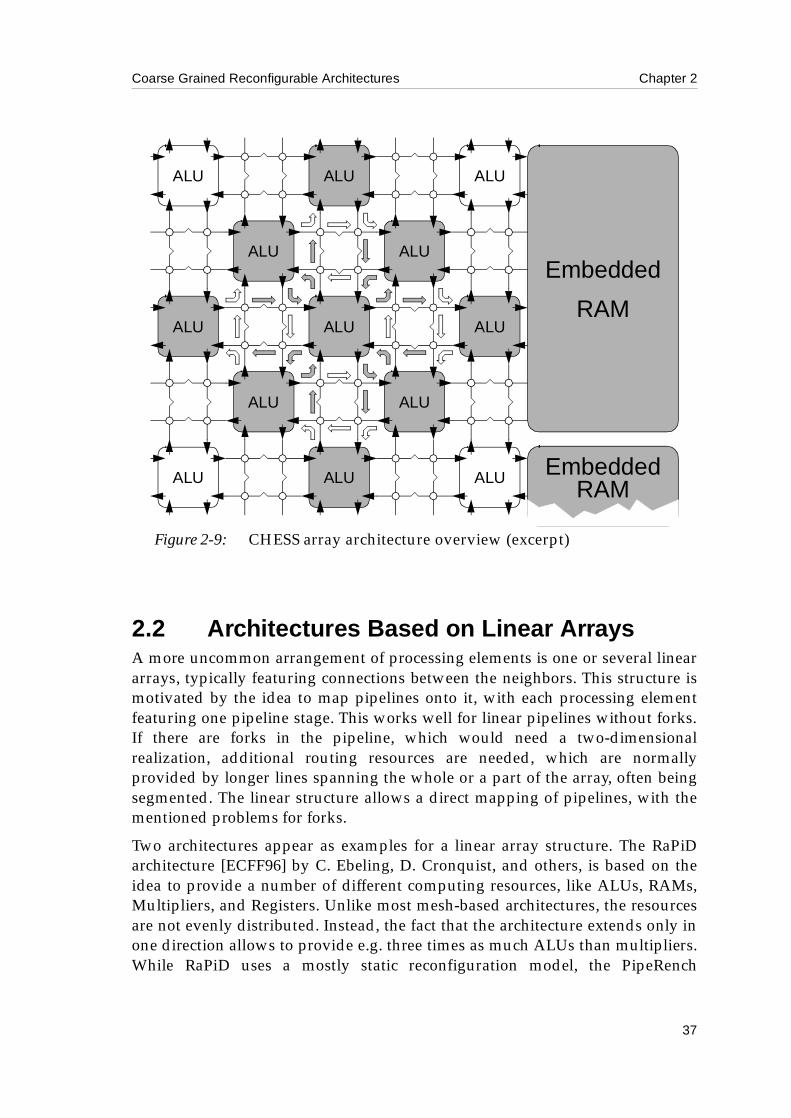
2.1.9 The CHESS ArrayThe CHESS architecture [MVS99] by Hewlett Packard Laboratories wasintroduced in 1999 and is intended for the implementation of multimediaapplications. CHESS is aimed as a component of an ASIC or processor datapath.
An overview of the CHESS array is given in figure 2-9. The architecture consistsof ALUs and switchboxes. These components are arranged in a chessboard-likepattern with each switchbox being surrounded by four ALUs and each ALUbeing surrounded by four switchboxes. To support applications with memoryrequirements for intermediate results, embedded RAMs can be providedorganized in vertical stripes inside the array. Additionally, switchboxes can beconverted to 16 word by 4 bit RAMs if needed.
The ALUs and all routing resources are four bits wide. The ALUs feature twoinputs and one output for four-bit data words, as well as one single-bit input andone output for carry. The instruction set features 16 operations, including add andsubtract, nine logical operations, two multiplex operations and three tests usingthe carry bit as condition output. It is possible to connect the data output of anALU to the configuration input of another one. Thus, the functionality of an ALUcan be changed in a limited way on a cycle-per-cycle basis during runtime byconfiguration data generated inside the array. However, a way for partialconfiguration from outside is not provided. In order to enable operations, whichcannot be mapped onto an ALU or to make fine-grained interconnections notsupported by the four-bit wiring, the RAMs in the switchboxes can also be usedas a 4-input, 4-output LUT.
The routing structure of the CHESS array consists of segmented four-bit buses ofdifferent length. There are 16 buses in each row and column of the array. Fourbuses are for local connections, spanning one switchbox. Due to the chessboardlayout of the array, these local connections are sufficient to link an ALU to all ofits eight surrounding neighbors, as shown in figure 2-9 by the grey arrows. Inaddition to the four local buses, there are two buses of length 1, crossing one ALUand half a switchbox on either side. Longer buses have lengths of powers of 2. Abus of length 2n crosses 2n ALUs and half a switchbox on either side. These busesare laid out in pairs with the ends of one bus in the middle of the other one. Thereare four buses of length 2, and two buses of length 4, 8 and 16 respectively.
37
Coarse Grained Reconfigurable Architectures Chapter 2
2.2 Architectures Based on Linear ArraysA more uncommon arrangement of processing elements is one or several lineararrays, typically featuring connections between the neighbors. This structure ismotivated by the idea to map pipelines onto it, with each processing elementfeaturing one pipeline stage. This works well for linear pipelines without forks.If there are forks in the pipeline, which would need a two-dimensionalrealization, additional routing resources are needed, which are normallyprovided by longer lines spanning the whole or a part of the array, often beingsegmented. The linear structure allows a direct mapping of pipelines, with thementioned problems for forks.
Two architectures appear as examples for a linear array structure. The RaPiDarchitecture [ECFF96] by C. Ebeling, D. Cronquist, and others, is based on theidea to provide a number of different computing resources, like ALUs, RAMs,Multipliers, and Registers. Unlike most mesh-based architectures, the resourcesare not evenly distributed. Instead, the fact that the architecture extends only inone direction allows to provide e.g. three times as much ALUs than multipliers.While RaPiD uses a mostly static reconfiguration model, the PipeRench
Figure 2-9: CHESS array architecture overview (excerpt)
ALU ALU
ALU
ALU
ALU
ALU
ALU
ALU
ALU
ALU
ALU
ALU
ALU
Embedded
RAM
EmbeddedRAM
Chapter 2 Coarse Grained Reconfigurable Architectures
38
architecture [CWGS98] relies on dynamic reconfiguration, allowing theconfiguration of a processing element to change in each execution cycle. Besidesmostly unidirectional nearest neighbor connects, this architecture provides also aglobal bus for data transfer.
2.2.1 The Reconfigurable Pipelined DatapathsThe Reconfigurable Pipelined Datapath (RaPiD) described in [ECFF96], [ECF96],[CFFF99] was developed in 1996 by Ebeling et al. It is aimed to speed up highlyregular, computation-intensive tasks by implementing deep application-specificpipelines.
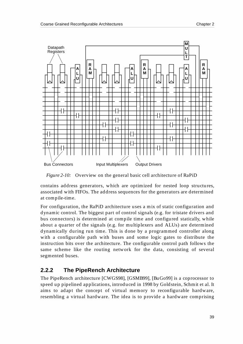
RaPiD provides a number of computational resources like ALUs, multipliers,registers and memory modules, which can implement application-specificdatapaths. These resources are arranged in a linear array, which is configured toform a mostly linear pipeline. This array is divided into identical basic cells,which are replicated to form a whole array. The RaPiD-1 prototype features 16cells, each cell containing an integer multiplier, three integer ALUs, six general-purpose datapath registers and three local memories with 32 entries. Alldatapaths as well as the memories are 16 bits wide. The ALUs are capable of theusual logical and arithmetic integer operations and can be chained for wide-integer operations. The multiplier processes two 16 bit input data words to one32 bit output word. The datapath registers can be used to store constants ortemporary values, to implement additional multiplexers, to support routing, andfor additional pipeline delays. The local memories can be used for block orienteddata processing. Each memory has a specialized datapath register featuring anincrementing feedback path. An overview on the general basic cell architecture isgiven in figure 2-10.
The routing architecture of the RaPiD consists of several parallel segmented 16 bitbuses, which span the whole array. The length of the bus segments varies indifferent tracks. In some tracks, adjacent bus segments can be merged byconfigurable bus connectors (see figure 2-10), which can also implement pipelinedelays if needed. The functional units can access all buses for reading and writingdata. For reading from the bus, each functional unit features an input multiplexerof n:1. One multiplexer input is reserved for constant zero, another one for afeedback line (the latter one does not appear any more in [CFFF99]). Thus, n-2inputs are for the buses, and therefore the number of buses is also n-2. The outputdrivers can put the result of a functional unit onto one or more bus segments.
The data to be processed enters and leaves RaPiD via I/O streams at each end ofthe datapath. For this purpose, the linear array is accompanied by a streamgenerator, which also contains the memory interface. The stream generator
39
Coarse Grained Reconfigurable Architectures Chapter 2
contains address generators, which are optimized for nested loop structures,associated with FIFOs. The address sequences for the generators are determinedat compile-time.
For configuration, the RaPiD architecture uses a mix of static configuration anddynamic control. The biggest part of control signals (e.g. for tristate drivers andbus connectors) is determined at compile time and configured statically, whileabout a quarter of the signals (e.g. for multiplexers and ALUs) are determineddynamically during run time. This is done by a programmed controller alongwith a configurable path with buses and some logic gates to distribute theinstruction bits over the architecture. The configurable control path follows thesame scheme like the routing network for the data, consisting of severalsegmented buses.
2.2.2 The PipeRench ArchitectureThe PipeRench architecture [CWGS98], [GSMB99], [BuGo99] is a coprocessor tospeed up pipelined applications, introduced in 1998 by Goldstein, Schmit et al. Itaims to adapt the concept of virtual memory to reconfigurable hardware,resembling a virtual hardware. The idea is to provide a hardware comprising
ALU
RAM
MULT
ALU
RAM
ALU
RAM
Bus Connectors Input Multiplexers Output Drivers
DatapathRegisters
Figure 2-10: Overview on the general basic cell architecture of RaPiD
Chapter 2 Coarse Grained Reconfigurable Architectures
40
several reconfigurable pipeline stages (called stripes in PipeRench terminology).An application pipeline is mapped onto the PipeRench, whereby the physicalhardware is kept transparent to the application. This is done by removingtemporary unused pipeline segments from the hardware, if necessary, thusimplementing a time multiplexing of the physical computation resources.According to this concept, the PipeRench relies highly on fast partial dynamicpipeline reconfiguration as well as run time scheduling of both configurationstreams and data streams.
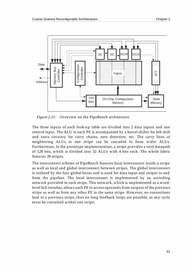
An overview of the architecture is given in figure 2-11. The PipeRench consists ofa reconfigurable fabric, a configuration memory, a state memory, an addresstranslation table (ATT), four data controllers, a memory bus controller and aconfiguration controller. The configuration memory is on-chip and connected tothe fabric with a wide bus, enabling one complete pipeline stage to be configuredwith one memory read. In a prototype described in [CWGS98], the configurationmemory has a capacity of 256 entries with 1024 bits each. The state memory isused to save the current register contents of a stripe, if it is swapped out. Theaddress translation table is used for storing the address in the state memory forthe state of a given stripe. The four data controllers are connected to the fabric byfour global buses. Each of the buses is dedicated to either the storing of a stripestate, the restoring of a state, the input of data or the output of data. Thecontrollers may all be used for data input or output where they interface betweenthe fabric and the memory bus controller. For the task of state storing andrestoring, only the two rightmost controllers may be employed, which act asinterface between the fabric and state memory, when used this way. The datacontrollers are also responsible for the generation of address sequences for bothinput and output data streams. This task includes the run time scheduling ofmemory accesses. The address sequences that can be generated are affinefunctions of the loop index. The data controllers may also contain caches toexploit locality or FIFOs to enhance burst mode memory accesses. The memorybus controller handles access of the data controllers to off-chip memory byarbitrating accesses to a single memory bus. This unit is also used to load theconfiguration memory. The configuration controller is responsible for the tasks ofinterfacing the fabric to the host, mapping of the configuration words to thehardware, run time scheduling (including time multiplexing and handling of thevirtualization), and managing the configuration memory.
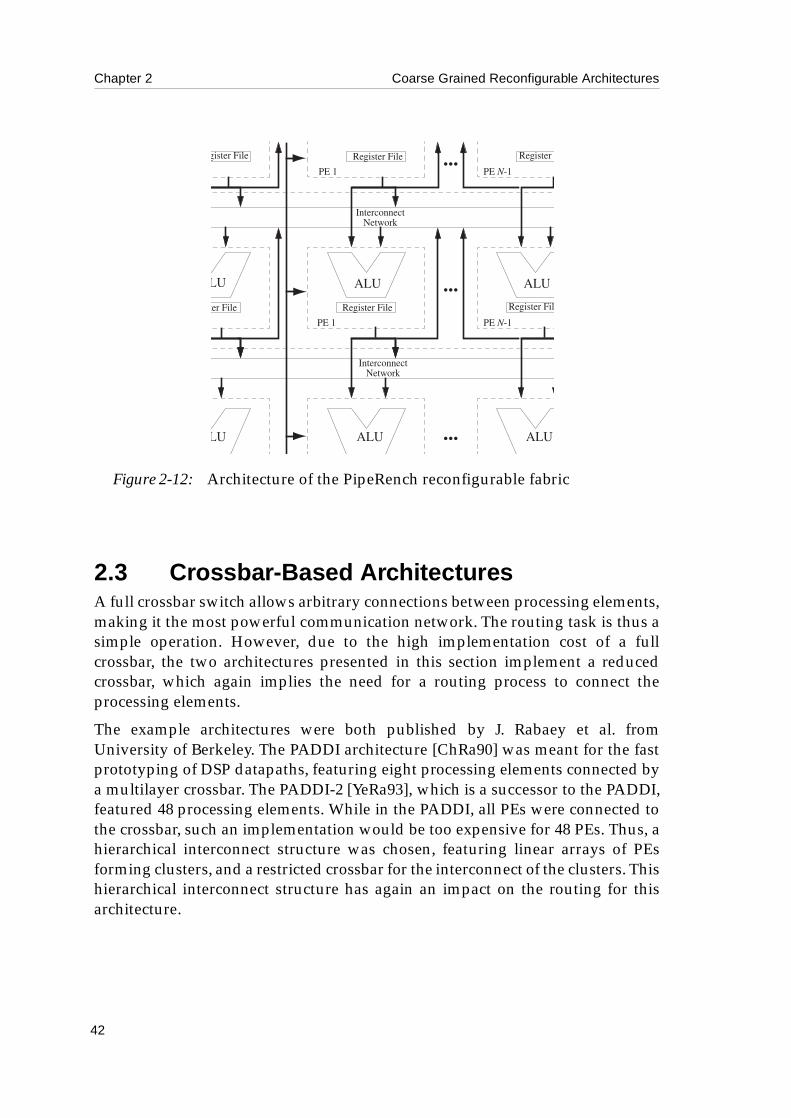
The reconfigurable fabric of the PipeRench allows the configuration of a pipelinestage in every cycle, while concurrently executing all other stages. Thearchitecture of the reconfigurable fabric is sketched in figure 2-12. The fabricconsists of several (horizontal) stripes. Each stripe is composed of interconnectand processing elements (PEs in figure 2-12), which contain registers and ALUs.The ALUs are implemented as 3-input lookup tables (one for each datapath bit).
41
Coarse Grained Reconfigurable Architectures Chapter 2
The three inputs of each look-up table are divided into 2 data inputs and onecontrol input. The ALU in each PE is accompanied by a barrel shifter for left shiftand extra circuitry for carry chains, zero detection, etc. The carry lines ofneighboring ALUs in one stripe can be cascaded to form wider ALUs.Furthermore, In the prototype implementation, a stripe provides a total datapathof 128 bits, which is divided into 32 ALUs with 4 bits each. The whole fabricfeatures 28 stripes.
The interconnect scheme of PipeRench features local interconnect inside a stripeas well as local and global interconnect between stripes. The global interconnectis realized by the four global buses and is used for data input and output to andfrom the pipeline. The local interconnect is implemented by an accordingnetwork provided in each stripe. This network, which is implemented as a word-level full crossbar, allows each PE to access operands from outputs of the previousstripe as well as from any other PE in the same stripe. However, no connectionslead to a previous stripe, thus no long feedback loops are possible, as any cyclemust be contained within one stripe.
State Memory
Ctrl Bits
Fabric AT
T
Mem
ory
Bus
Con
trol
ler
Con
figur
atio
n C
ontr
olle
r
Data
Address
On-Chip ConfigurationMemory
DC DC DC/R DC/S
Figure 2-11: Overview on the PipeRench architecture
Chapter 2 Coarse Grained Reconfigurable Architectures
42
2.3 Crossbar-Based ArchitecturesA full crossbar switch allows arbitrary connections between processing elements,making it the most powerful communication network. The routing task is thus asimple operation. However, due to the high implementation cost of a fullcrossbar, the two architectures presented in this section implement a reducedcrossbar, which again implies the need for a routing process to connect theprocessing elements.
The example architectures were both published by J. Rabaey et al. fromUniversity of Berkeley. The PADDI architecture [ChRa90] was meant for the fastprototyping of DSP datapaths, featuring eight processing elements connected bya multilayer crossbar. The PADDI-2 [YeRa93], which is a successor to the PADDI,featured 48 processing elements. While in the PADDI, all PEs were connected tothe crossbar, such an implementation would be too expensive for 48 PEs. Thus, ahierarchical interconnect structure was chosen, featuring linear arrays of PEsforming clusters, and a restricted crossbar for the interconnect of the clusters. Thishierarchical interconnect structure has again an impact on the routing for thisarchitecture.
LU
LU
ter File
ALU
ALU
PE 1
PE 1
Interconnect
ALU
ALU
PE N-1
PE N-1
...
...
...gister File Register File Register F
Register File Register Fil
Network
InterconnectNetwork
Figure 2-12: Architecture of the PipeRench reconfigurable fabric
43
Coarse Grained Reconfigurable Architectures Chapter 2
2.3.1 The Programmable Arithmetic Device for Digital Signal Processing
The PADDI (Programmable Arithmetic Device for Digital Signal Processing)architecture was first described in 1990 by Chen and Rabaey [ChRa90], [ChRa92],[CGNS92a]. PADDI addresses the problem of rapid prototyping for computation-intensive DSP data paths.
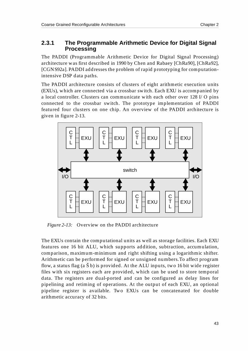
The PADDI architecture consists of clusters of eight arithmetic execution units(EXUs), which are connected via a crossbar switch. Each EXU is accompanied bya local controller. Clusters can communicate with each other over 128 I/O pinsconnected to the crossbar switch. The prototype implementation of PADDIfeatured four clusters on one chip. An overview of the PADDI architecture isgiven in figure 2-13.
The EXUs contain the computational units as well as storage facilities. Each EXUfeatures one 16 bit ALU, which supports addition, subtraction, accumulation,comparison, maximum-minimum and right shifting using a logarithmic shifter.Arithmetic can be performed for signed or unsigned numbers. To affect programflow, a status flag (a Š b) is provided. At the ALU inputs, two 16 bit wide registerfiles with six registers each are provided, which can be used to store temporaldata. The registers are dual-ported and can be configured as delay lines forpipelining and retiming of operations. At the output of each EXU, an optionalpipeline register is available. Two EXUs can be concatenated for doublearithmetic accuracy of 32 bits.
EXUCTL
EXUCTL
EXUCTL
EXUCTL
EXUCTL
EXUCTL
EXUCTL
EXUCTL
switchI/OI/O
Figure 2-13: Overview on the PADDI architecture
Chapter 2 Coarse Grained Reconfigurable Architectures
44
For the interconnection of the EXUs, a crossbar switch is employed, which is usedfor routing both data and status flags. While the data routing can be changed ineach cycle dynamically at run time, the routing of the status flags is static anddetermined at compile time.
The control of the architecture is done hierarchically in order to handle therelatively high instruction bandwidth for all eight EXUs. On a first level, anexternal global controller broadcasts 3 bit global instructions to each EXU. Theinstructions from the global controller are decoded on a second level by localcontrol units in each EXU into a 53 bit instruction word. The local controllers ineach EXU are SRAM-based nanostores, which are serially configured at setup-time. Each SRAM contains eight words, allowing eight different operations to beperformed. The execution units and the external controller communicate statusinformation to affect both the local and global control flow.
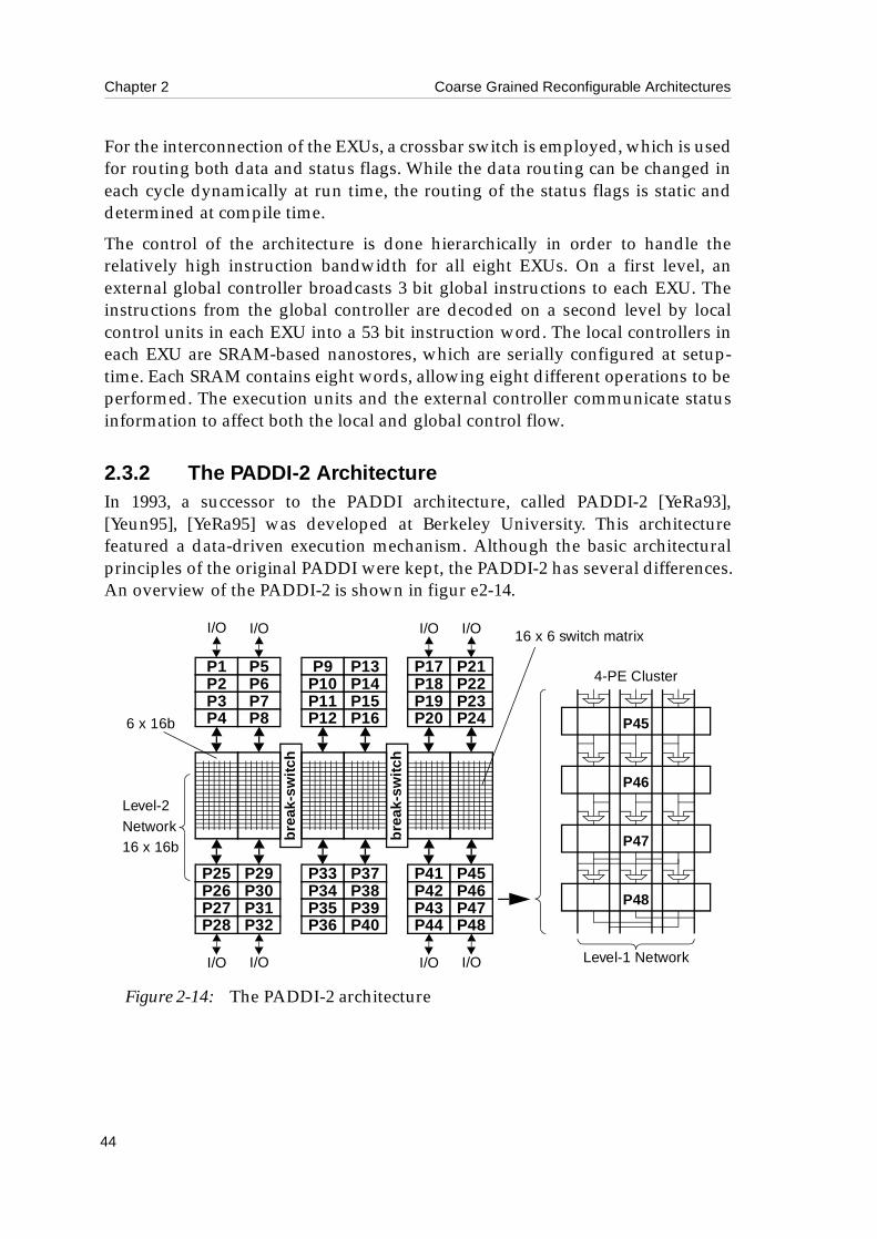
2.3.2 The PADDI-2 ArchitectureIn 1993, a successor to the PADDI architecture, called PADDI-2 [YeRa93],[Yeun95], [YeRa95] was developed at Berkeley University. This architecturefeatured a data-driven execution mechanism. Although the basic architecturalprinciples of the original PADDI were kept, the PADDI-2 has several differences.An overview of the PADDI-2 is shown in figur e2-14.
Figure 2-14: The PADDI-2 architecture
NetworkP47
P48
P46
P45
P1P2P3P4
P5P6P7P8
P9P10P11P12
P13P14P15P16
P17P18P19P20
P21P22P23P24
P25P26P27P28
P29P30P31P32
P33P34P35P36
P37P38P39P40
P41P42P43P44
P45P46P47P48
bre
ak-s
wit
ch
bre
ak-s
wit
ch
I/O I/O I/O I/O
I/O I/O I/O I/O
6 x 16b
16 x 6 switch matrix
Level-2
16 x 16b
Level-1 Network
4-PE Cluster
45
Coarse Grained Reconfigurable Architectures Chapter 2
The PADDI-2 has been implemented on a chip featuring 48 processing elements(or EXUs in original PADDI terminology) with a 16 bit datapath. Each processingelement features a 16 bit ALU with 12 instructions including add, add with carry-in, subtract, subtract with carry-in, logical or, logical and, logical xor, logical not,arithmetic up shift, arithmetic down shift, booth multiply and select.Multiplication can be done in eight cycles on a single processor. Alternatively,eight processors can be pipelined, resulting in one multiplication product inevery cycle. Using the carry-in, the add and subtract operations can beconcatenated for datapaths with a width of a multiple of 16 bits. Each processingelement provides also six general purpose registers, which can be configured asup to three input queues for the ALU, three scratch pad registers and aninstruction memory (nanostore) with eight entries as well as a control unit.
In contrast to the original PADDI architecture, the processing elements of PADDI-2 are packed in 12 clusters of four elements each. Thus, the interconnect ishierarchical with two levels. On the first level, each cluster features six 16 bit databuses and four one bit control buses, providing intra-cluster interconnect. On thesecond level, 16 data buses and eight control buses can be used for inter-clusterinterconnect. They can be broken up into shorter segments by reconfigurableswitches. The eight clusters in the corners of the chip provide additional I/Oconnections to the outside. As the crossbar switch of the original PADDI forarbitrary connections between processing elements has been given up, theplacement and routing for PADDI-2 is more sophisticated.
The PADDI-2 architecture employs a distributed data-driven control strategy[YeRa92] implemented by a hardware handshake protocol for synchronization. Ifa sender or a receiver is not ready for a data transfer, all participants are stalled.By this mechanism, the need for global synchronization and retiming during themapping process is eliminated.

Chapter 2 Coarse Grained Reconfigurable Architectures
46