Embed Size (px)
Citation preview

http://introcs.cs.princeton.edu
R O B E R T S E D G E W I C K K E V I N W A Y N E
Com
puter Science
ComputerScience
An Interdisciplinary Approach
20. Central Processing Unit
COMPUTER SC I ENCE S E D G E W I C K / W A Y N E
PART I I : ALGORITHMS, MAC HINES , and THEORY
Sections 6.3−4

20. CPU
•Overview •Bits, registers, and memory •Program counter •Components and connections
COMPUTER SC I ENCE S E D G E W I C K / W A Y N E
PART I I : ALGORITHMS, MAC HINES , and THEORY
CS.20.A.CPU.Overview
Let's build a computer!
CPU = Central Processing Unit
Computer Display Touchpad Battery Keyboard ... CPU (difference between a TV set and a computer)
Previous lecture Combinational circuits ALU (calculator)
This lecture Sequential circuits with memory CPU (computer)
3
CPU
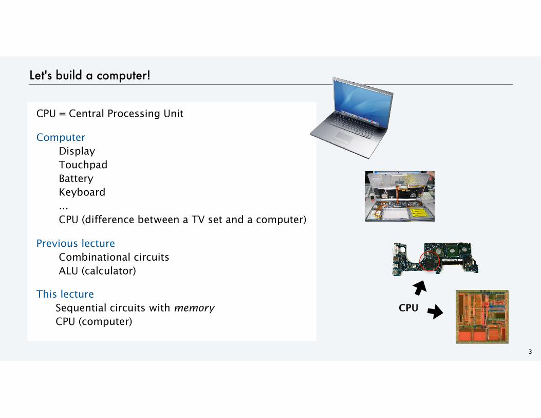
A smaller computing machine: TOY-8
TOY instruction-set architecture. • 256 16-bit words of memory. • 16 16-bit registers. • 1 8-bit program counter. • 2 instruction types. • 16 instructions.
TOY-8 instruction-set architecture. • 16 8-bit words of memory. • 1 8-bit register. • 1 4-bit program counter. • 1 instruction type. • 8 instructions.
4
4 bits to specify one of 16 registers
8 bits to specify one of 256 memory words
Type 1 instructionopcode Rd Rs Rt
Type 2 instructionopcode Rd addr
Purpose of TOY-8. Illustrate CPU circuit design for a "typical" computer.
4 bits to specify one of 16 memory words
TOY-8 instructionopcode addr
0
3 bits to specifyone of 8 instructions
always 0 (future expansion of memory or instruction set)
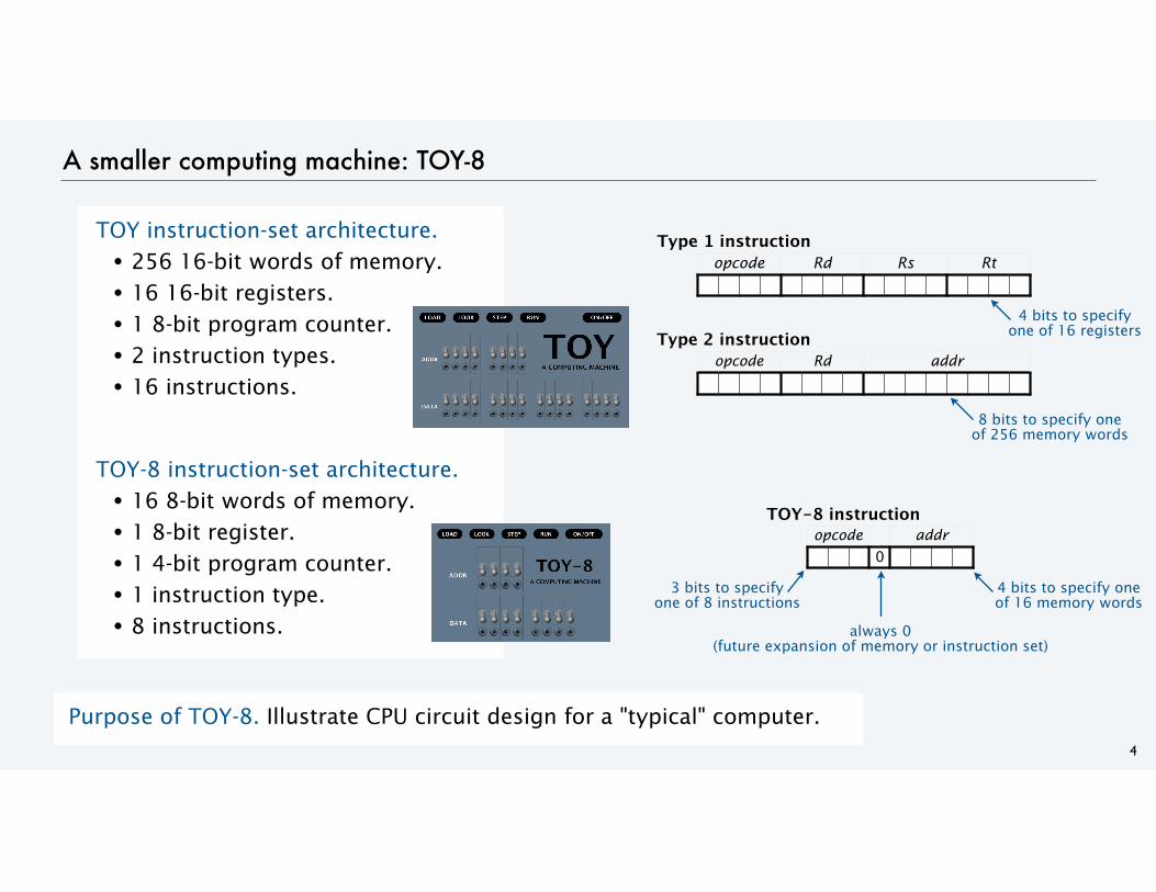
TOY-8 reference card
5
opcode addr0
PC
1
opcode operation pseudo-code
0 halt halt
2 add R = R + M[addr]
4 bitwise and R = R & M[addr]
6 bitwise xor R = R ^ M[addr]
8 load addr R = addr
A load R = M[addr]
C store M[addr] = R
E branch zero if (R == 0) PC = addr
ZERO M[0] is always 0.
STANDARD INPUT Load from M[F].
STANDARD OUTPUT Store to M[F].
Memory
R = M[5]R = R + M[6]M[7] = R
halt
1 A 52 2 63 C 74 0 05 0 56 0 87
...
A TOY-8 program
R 0 50 D
0 D
234
Challenge for the bored:
Write Fibonacci seq, add numbers on stdin, ...
Add two numbers from memory and put sum in memory
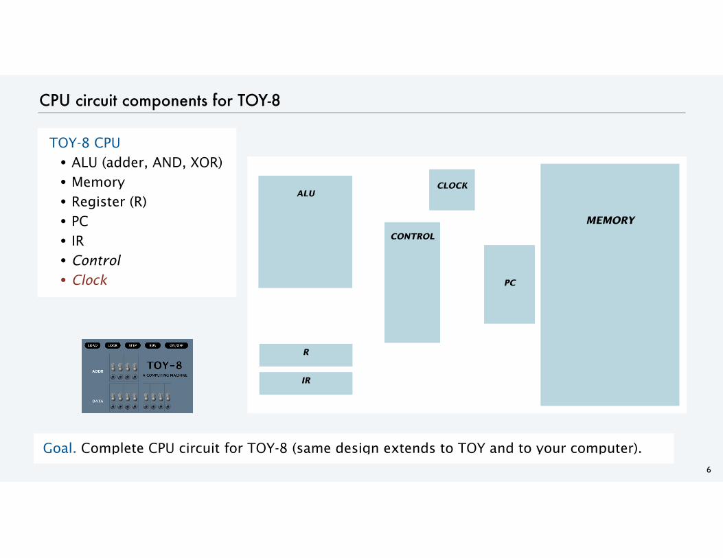
CPU circuit components for TOY-8
TOY-8 CPU • ALU (adder, AND, XOR) • Memory • Register (R) • PC • IR • Control • Clock
6
CLOCK
MEMORY
ALU
R
IR
PC
CONTROL
Goal. Complete CPU circuit for TOY-8 (same design extends to TOY and to your computer).

Review: Components, busses, and control lines
Basic design of our circuits • Organized as components (functional units of TOY: ALU, memory, register, PC, and IR). • Connected by busses (groups of wires that propagate information between components). • Controlled by control lines (single wires that control circuit behavior).
7
Conventions • Bus inputs are at the top,
input connections are at the left. • Bus outputs are at the bottom,
output connections are at the right. • Control lines are blue.
These conventions make circuits easy to understand. (Like style conventions in coding.)
output bus
input busses
control lines

Perspective
Q. Why TOY-8?
A. TOY circuit width would be about 5 times TOY-8 circuit width.
8
TOY
TOY-8
Sobering fact. The circuit for your computer is hundreds to thousands of times wider.
Reassuring fact. Design of all three is based on the same fundamental ideas.
C O M P U T E R S C I E N C E S E D G E W I C K / W A Y N E
CS.20.A.CPU.Overview
20. CPU
•Overview •Bits, registers, and memory •Program counter •Connections
COMPUTER SC I ENCE S E D G E W I C K / W A Y N E
PART I I : ALGORITHMS, MAC HINES , and THEORY
CS.20.B.CPU.Memory
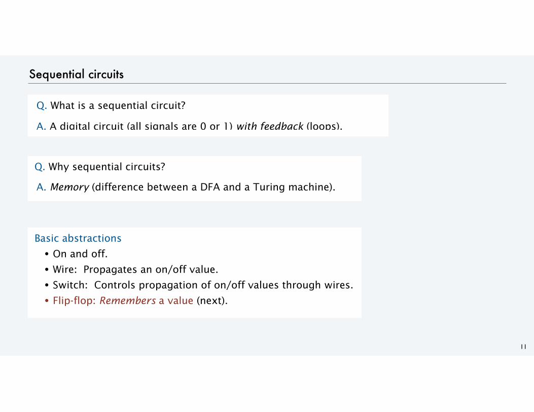
Sequential circuits
Q. What is a sequential circuit?
A. A digital circuit (all signals are 0 or 1) with feedback (loops).
11
Q. Why sequential circuits?
A. Memory (difference between a DFA and a Turing machine).
Basic abstractions
• On and off.
• Wire: Propagates an on/off value.
• Switch: Controls propagation of on/off values through wires.
• Flip-flop: Remembers a value (next).
12
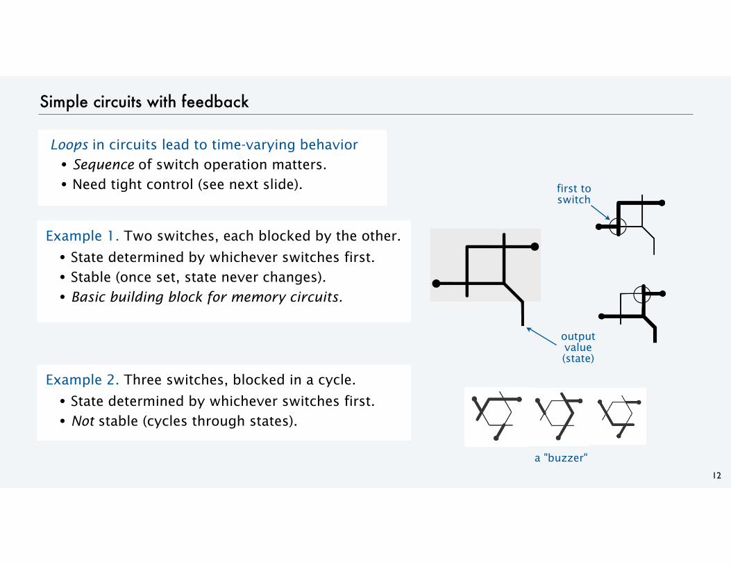
Simple circuits with feedback
Loops in circuits lead to time-varying behavior • Sequence of switch operation matters. • Need tight control (see next slide).
a "buzzer"
Example 1. Two switches, each blocked by the other.
• State determined by whichever switches first. • Stable (once set, state never changes). • Basic building block for memory circuits.
Example 2. Three switches, blocked in a cycle.
• State determined by whichever switches first. • Not stable (cycles through states).
output value (state)
first to switch
13
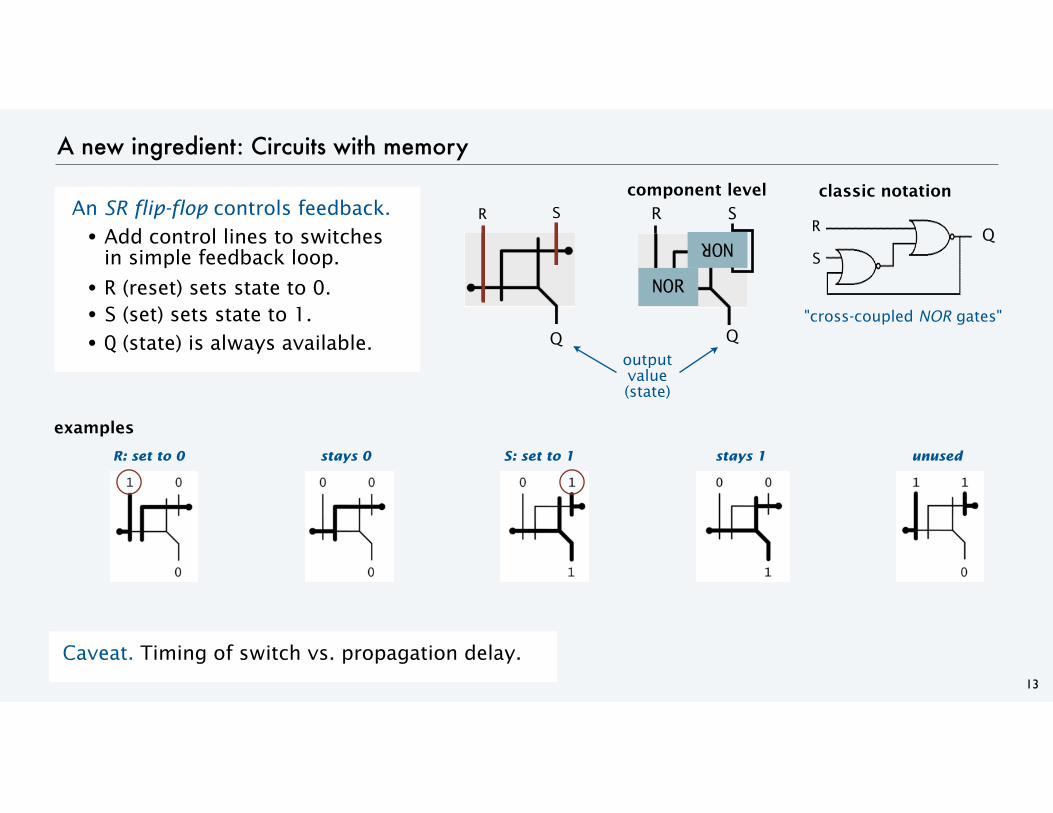
A new ingredient: Circuits with memory
An SR flip-flop controls feedback. • Add control lines to switches
in simple feedback loop.
• R (reset) sets state to 0. • S (set) sets state to 1. • Q (state) is always available.
NOR
S
Q
component level
NOR
R
Caveat. Timing of switch vs. propagation delay.
stays 0 stays 1 unused
SR
Qoutput value (state)
QR
S
classic notation
"cross-coupled NOR gates"
examplesR: set to 0 S: set to 1

14
Flip-flop application: Memory bit
Add logic to an SR flip-flop for more precise control • Provide data value on an input wire instead of using S and R controls. • Use WRITE control wire to enable change in flip-flop value. • Flip-flop value always available as output.
1
WRITE on
set to 1
S
stays 1
WRITE off
set to 0 0
WRITE on
R
stays 0
WRITE off
MEMORY BIT
input
WRITE
output
FETCH
CLOCK
EXECUTE
RUN
HALT
15
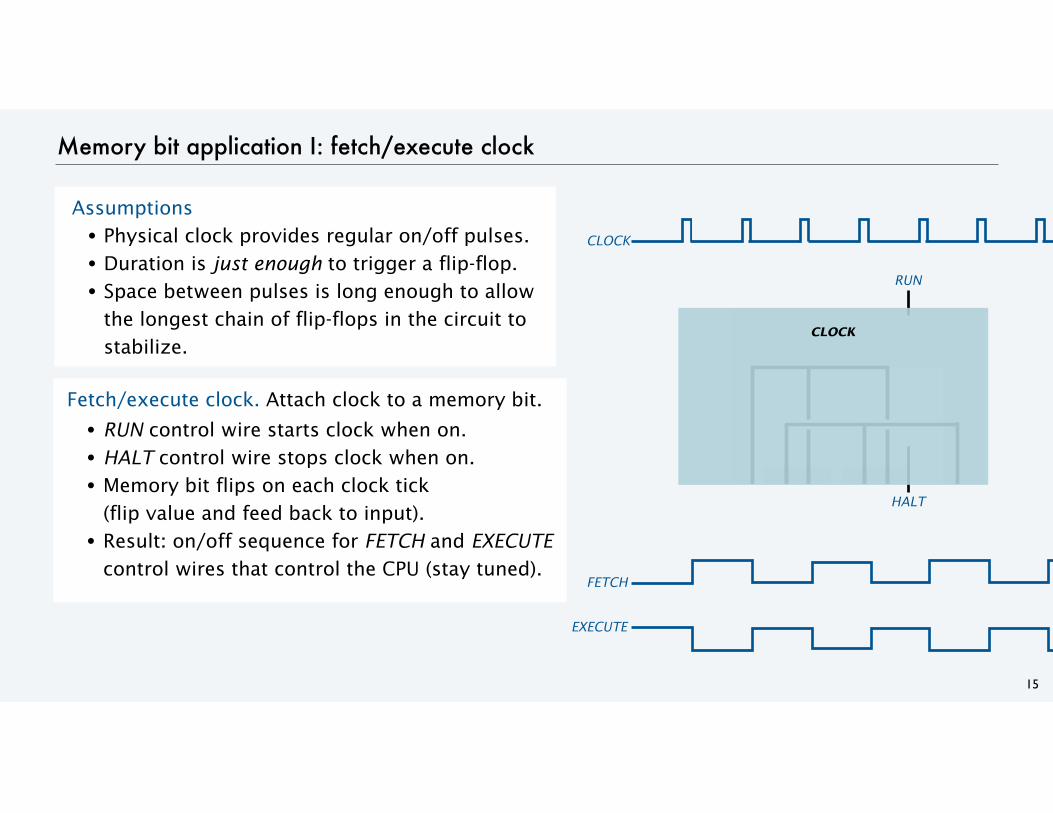
Memory bit application I: fetch/execute clock
Assumptions • Physical clock provides regular on/off pulses. • Duration is just enough to trigger a flip-flop. • Space between pulses is long enough to allow
the longest chain of flip-flops in the circuit to stabilize.
Fetch/execute clock. Attach clock to a memory bit.
• RUN control wire starts clock when on. • HALT control wire stops clock when on. • Memory bit flips on each clock tick
(flip value and feed back to input). • Result: on/off sequence for FETCH and EXECUTE
control wires that control the CPU (stay tuned).
CLOCK
FETCH
EXECUTE
CLOCK
16
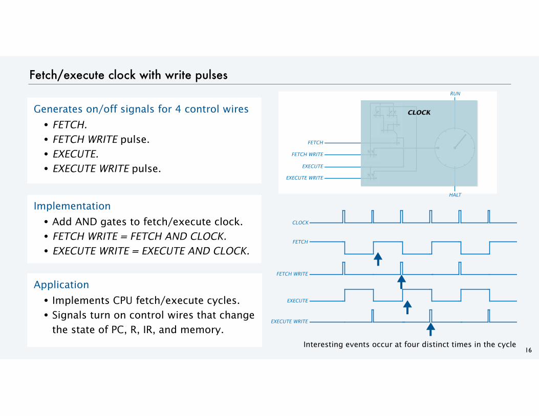
Fetch/execute clock with write pulses
Generates on/off signals for 4 control wires
• FETCH. • FETCH WRITE pulse. • EXECUTE. • EXECUTE WRITE pulse.
RUN
HALT
FETCH WRITE
FETCH
FETCH
FETCH WRITE
EXECUTE
EXECUTE WRITE
CLOCK
EXECUTE
EXECUTE WRITE
Implementation
• Add AND gates to fetch/execute clock. • FETCH WRITE = FETCH AND CLOCK. • EXECUTE WRITE = EXECUTE AND CLOCK.
Application
• Implements CPU fetch/execute cycles. • Signals turn on control wires that change
the state of PC, R, IR, and memory.
CLOCK
Interesting events occur at four distinct times in the cycle
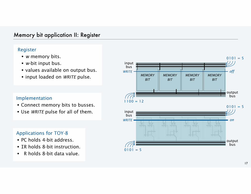
Memory bit application II: Register
Register • w memory bits. • w-bit input bus. • values available on output bus. • input loaded on WRITE pulse.
17
0101 = 5input bus
Implementation • Connect memory bits to busses. • Use WRITE pulse for all of them.
Applications for TOY-8 • PC holds 4-bit address. • IR holds 8-bit instruction. • R holds 8-bit data value.
WRITE offMEMORY
BITMEMORY
BITMEMORY
BITMEMORY
BIT
0101 = 5input bus
output bus
0101 = 5
WRITE on
output bus
1100 = 12
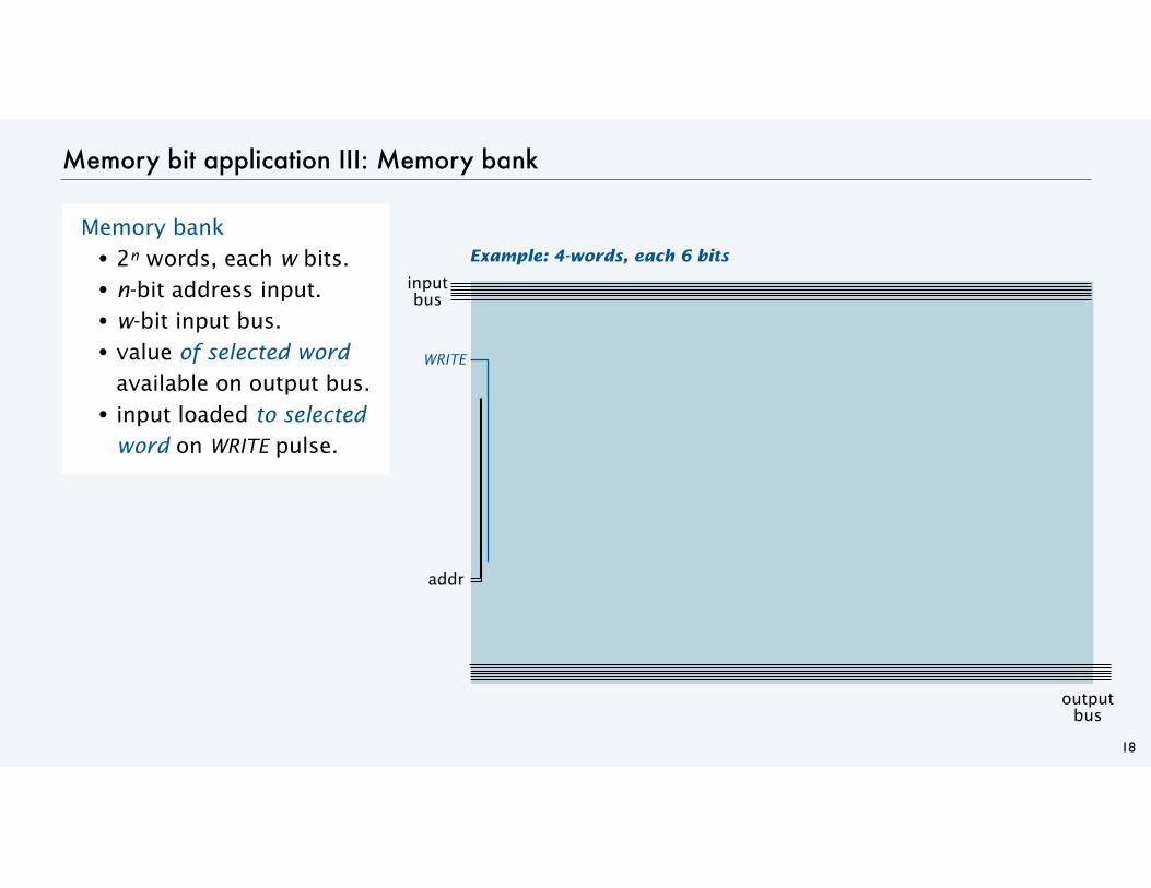
Memory bit application III: Memory bank
Memory bank • 2n words, each w bits. • n-bit address input. • w-bit input bus. • value of selected word
available on output bus. • input loaded to selected
word on WRITE pulse.
18
Example: 4-words, each 6 bits
WRITE
input bus
addr
output bus
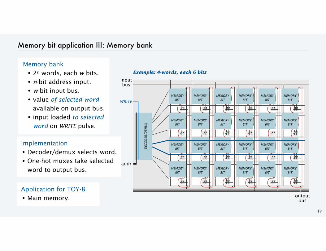
Memory bit application III: Memory bank
Memory bank • 2n words, each w bits. • n-bit address input. • w-bit input bus. • value of selected word
available on output bus. • input loaded to selected
word on WRITE pulse.
19
Implementation • Decoder/demux selects word. • One-hot muxes take selected
word to output bus.
Application for TOY-8 • Main memory.
Example: 4-words, each 6 bits
MEMORY BIT
MEMORY BIT
MEMORY BIT
MEMORY BIT
MEMORY BIT
MEMORY BIT
MEMORY BIT
MEMORY BIT
MEMORY BIT
MEMORY BIT
MEMORY BIT
MEMORY BIT
MEMORY BIT
MEMORY BIT
MEMORY BIT
MEMORY BIT
MEMORY BIT
MEMORY BIT
MEMORY BIT
MEMORY BIT
MEMORY BIT
MEMORY BIT
MEMORY BIT
MEMORY BIT
DEC
OD
ER/D
EMU
X
WRITE
input bus
addr
output bus
MEMORY 16 8-bit words
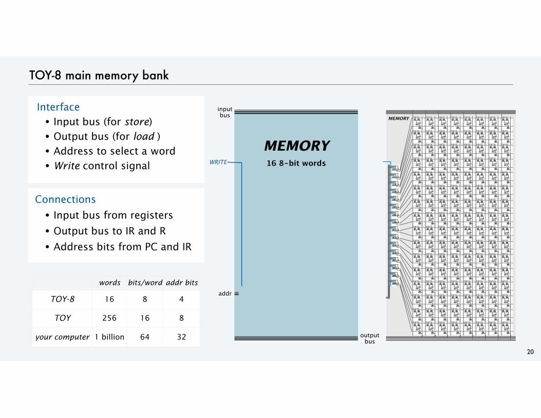
TOY-8 main memory bank
Interface • Input bus (for store) • Output bus (for load ) • Address to select a word • Write control signal
20
Connections
• Input bus from registers
• Output bus to IR and R
• Address bits from PC and IR
input bus
addr
MEMORY
output bus
WRITE
words bits/word addr bits
TOY-8 16 8 4
TOY 256 16 8
your computer 1 billion 64 32
C O M P U T E R S C I E N C E S E D G E W I C K / W A Y N E
CS.20.B.CPU.Memory
20. CPU
•Overview •Bits, registers, and memory •Program counter •Components and connections
COMPUTER SC I ENCE S E D G E W I C K / W A Y N E
PART I I : ALGORITHMS, MAC HINES , and THEORY
CS.20.C.CPU.PC
23
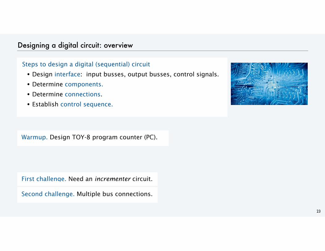
Designing a digital circuit: overview
Steps to design a digital (sequential) circuit
• Design interface: input busses, output busses, control signals.
• Determine components.
• Determine connections.
• Establish control sequence.
Warmup. Design TOY-8 program counter (PC).
First challenge. Need an incrementer circuit.
Second challenge. Multiple bus connections.
24
Pop quiz on combinational circuit design
Q. Design a circuit to compute x + 1.

25
Pop quiz on combinational circuit design
A. Start with a bitwise adder • Delete y inputs, set carry in to 1. • Compute carry with AND and sum with XOR.
Q. Design a circuit to compute x + 1.
c4 c3 c2 c1 1
+ x3 x2 x1 x0
z3 z2 z1 z0
xi ci ci+1
0 0 0
0 1 0
1 0 0
1 1 1
carry bit
xi ci zi
0 0 0
0 1 1
1 0 1
1 1 0
sum bit
AND
0
0
0
1
XOR
0
1
1
0x + 1
x
4-bit incrementer
XOR XOR XOR XOR
AND AND AND AND

R
ALU
MEMORY
Multiple bus connections
26
If component outputs go to multiple other components • No problem, just use T connections. • Values on both busses are the same. • Example: Register connects to ALU and memory.
If component inputs come from multiple other components • Problem. • Values on the busses are different. • Example: ALU, memory, and IR connect to register. • Solution: Need a selector switch (bus mux).
MEMORY
ALU
IR
R
?
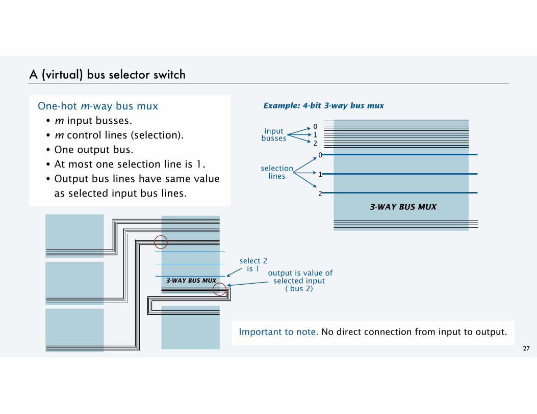
A (virtual) bus selector switch
One-hot m-way bus mux • m input busses. • m control lines (selection). • One output bus. • At most one selection line is 1. • Output bus lines have same value
as selected input bus lines.
27
3-WAY BUS MUX
input busses
0 1 2
0
1
2
selection lines
3-WAY BUS MUX
select 2 is 1 output is value of
selected input ( bus 2)
Important to note. No direct connection from input to output.
Example: 4-bit 3-way bus mux
0 1 2
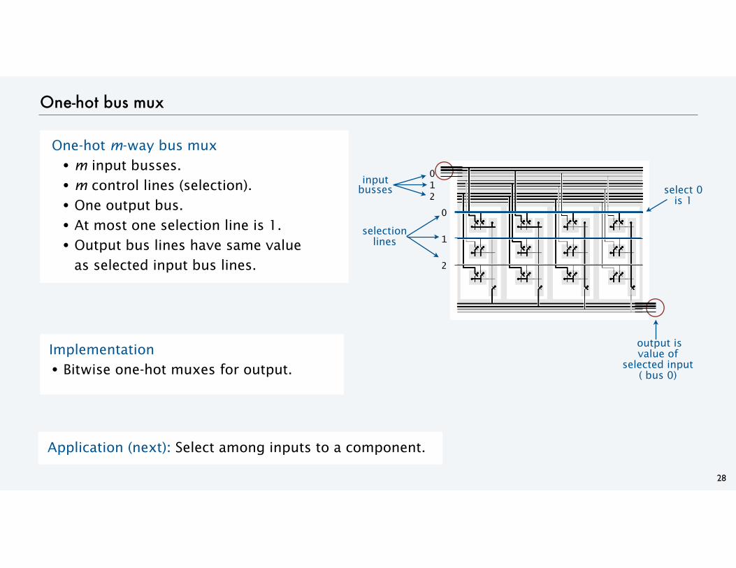
One-hot bus mux
28
Implementation • Bitwise one-hot muxes for output.
0
1
2
selection lines
select 0 is 1
output is value of
selected input ( bus 0)
input busses
Application (next): Select among inputs to a component.
One-hot m-way bus mux • m input busses. • m control lines (selection). • One output bus. • At most one selection line is 1. • Output bus lines have same value
as selected input bus lines.
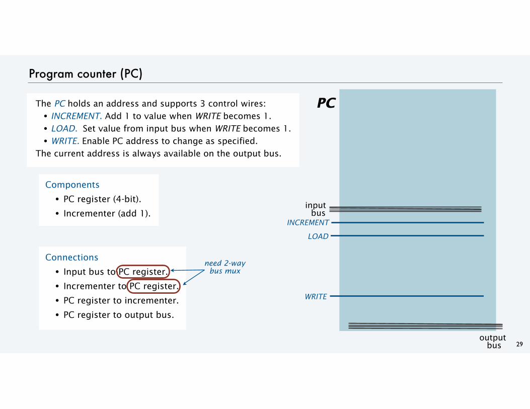
Components
• PC register (4-bit).
• Incrementer (add 1).
Connections
• Input bus to PC register.
• Incrementer to PC register.
• PC register to incrementer.
• PC register to output bus.
29
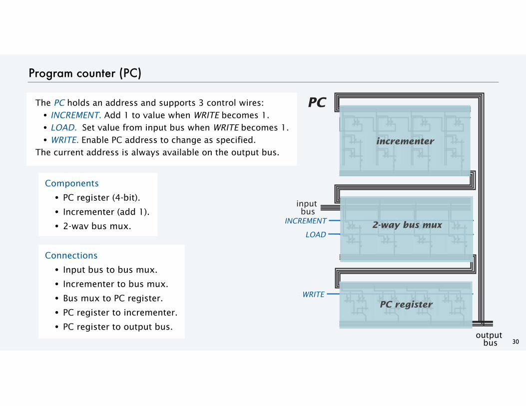
Program counter (PC)
The PC holds an address and supports 3 control wires: • INCREMENT. Add 1 to value when WRITE becomes 1. • LOAD. Set value from input bus when WRITE becomes 1. • WRITE. Enable PC address to change as specified.
The current address is always available on the output bus.
input bus
output bus
PC
need 2-way bus mux
INCREMENT
LOAD
WRITE
30
Program counter (PC)
The PC holds an address and supports 3 control wires: • INCREMENT. Add 1 to value when WRITE becomes 1. • LOAD. Set value from input bus when WRITE becomes 1. • WRITE. Enable PC address to change as specified.
The current address is always available on the output bus.
write
increment
outputbus
input bus
load
PC
incrementer
2-way bus mux
PC register
INCREMENT
LOAD
WRITE
output bus
Components
• PC register (4-bit).
• Incrementer (add 1).
• 2-way bus mux.
Connections
• Input bus to bus mux.
• Incrementer to bus mux.
• Bus mux to PC register.
• PC register to incrementer.
• PC register to output bus.

31
Summary of TOY-8 PC circuit
The PC supports two control-signal sequences: • Load, then write. Set address from input bus (example: branch instruction). • Increment, then write. Add one to value.
Address is written to the PC register in both cases and always available on the output bus.
Next. CPU circuit.
Important note: write pulse must be very short because of the cycle in this circuit.
write
increment
outputbus
input bus
load
PC
incrementer
2-way bus mux
PC registerwrite
loadLOAD
WRITE write
increment
outputbus
input bus
load
PC
incrementer
2-way bus mux
PC registerwrite
incrementINCREMENT
WRITE

C O M P U T E R S C I E N C E S E D G E W I C K / W A Y N E
CS.20.C.CPU.PC

20. CPU
•Overview •Bits, registers, and memory •Program counter •Components, connections, and control
COMPUTER SC I ENCE S E D G E W I C K / W A Y N E
PART I I : ALGORITHMS, MAC HINES , and THEORY
CS.20.D.CPU.Components
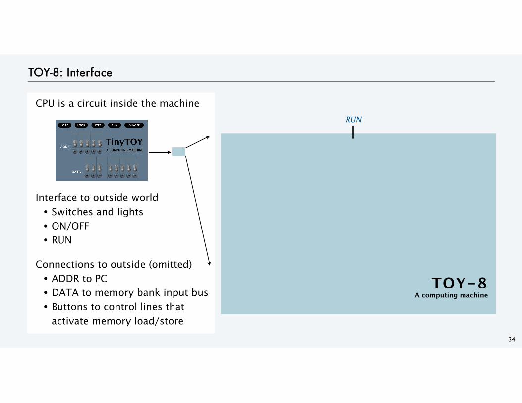
CPU is a circuit inside the machine
Interface to outside world • Switches and lights • ON/OFF • RUN
Connections to outside (omitted) • ADDR to PC • DATA to memory bank input bus • Buttons to control lines that
activate memory load/store
TOY-8: Interface
34
TOY-8A computing machine
RUN
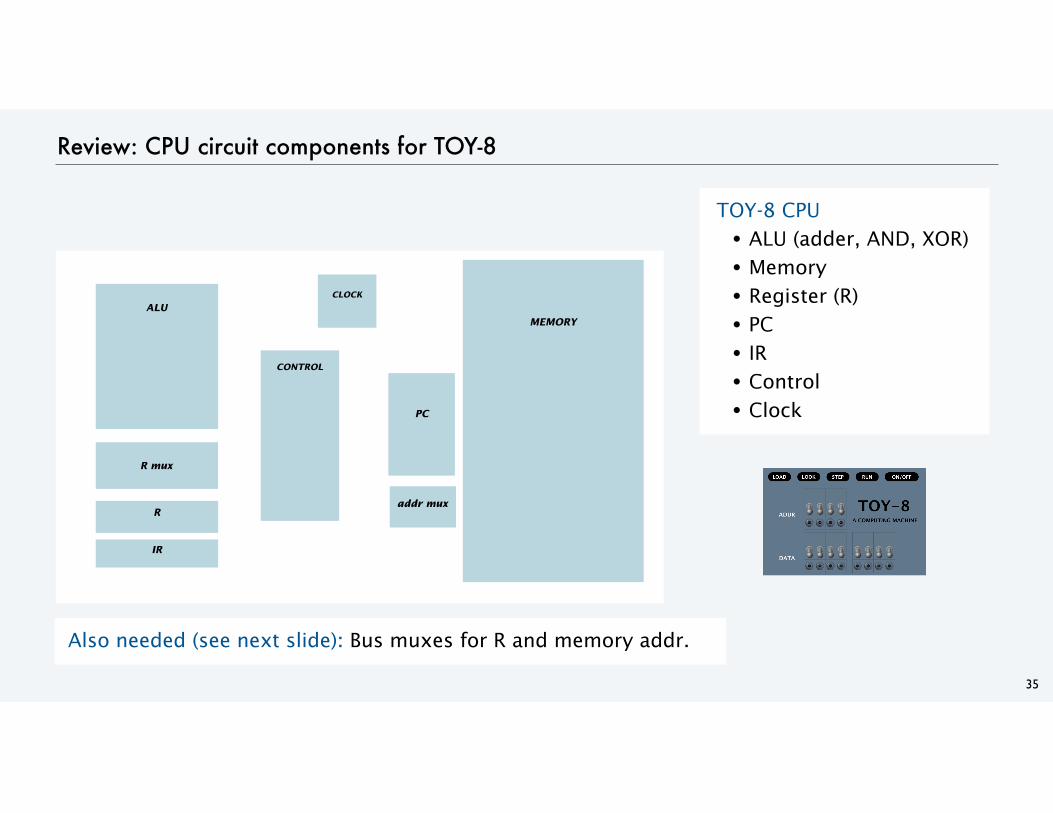
Review: CPU circuit components for TOY-8
TOY-8 CPU • ALU (adder, AND, XOR) • Memory • Register (R) • PC • IR • Control • Clock
35
CLOCK
MEMORYALU
R
IR
PC
CONTROL
R mux
addr mux
Also needed (see next slide): Bus muxes for R and memory addr.
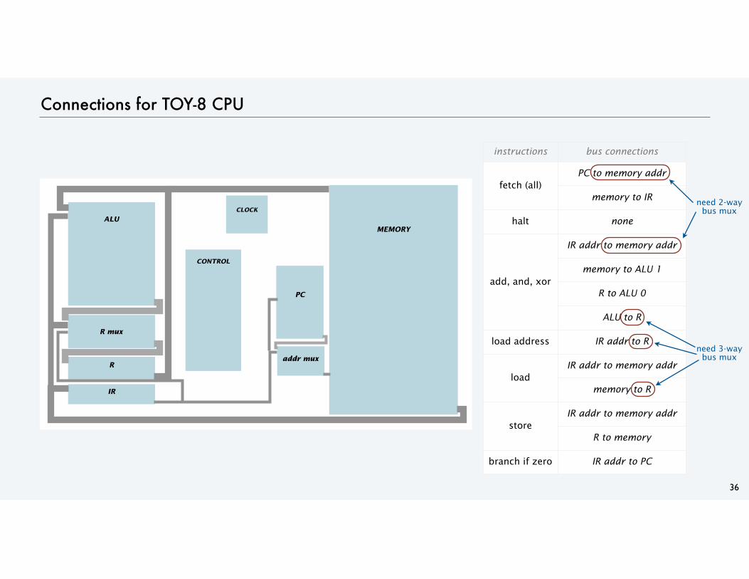
instructions bus connections
fetch (all)PC to memory addr
memory to IR
halt none
add, and, xor
IR addr to memory addr
memory to ALU 1
R to ALU 0
ALU to R
load address IR addr to R
loadIR addr to memory addr
memory to R
storeIR addr to memory addr
R to memory
branch if zero IR addr to PC
Connections for TOY-8 CPU
36
CLOCK
MEMORYALU
R
IR
PC
CONTROL
R mux
addr muxneed 3-way
bus mux
need 2-way bus mux
`
`
`

component control wires
CLOCKRUN
HALT
CONTROL
FETCH
FETCH WRITE
EXECUTE
EXECUTE WRITE
ALU
ADD
XOR
AND
R mux
R MUX ALU
R MUX MEM
R MUX IR
R R WRITE
IR IR WRITE
memory MEMORY WRITE
PCPC INCREMENT
PC LOAD
PC WRITE
addr muxADDR MUX PC
ADDR MUX IR
Control wires for TOY-8 CPU
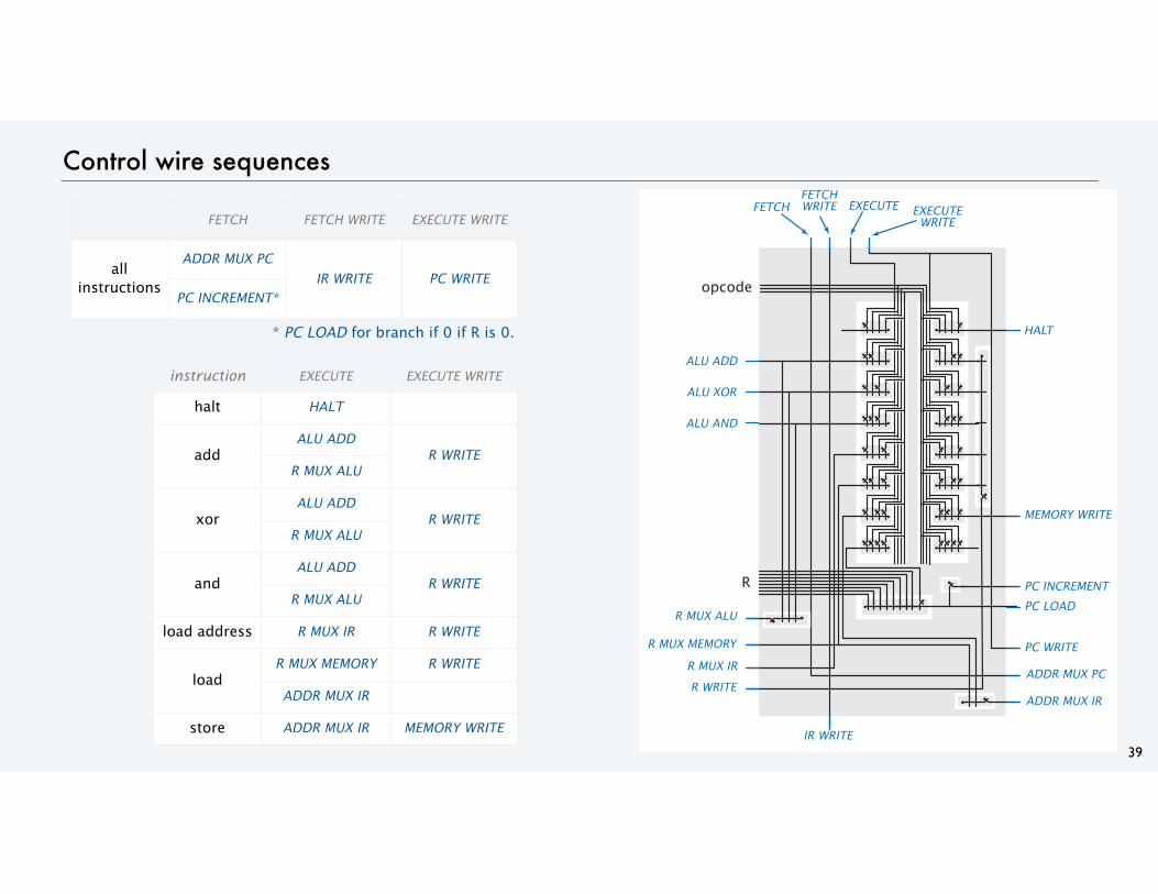
37
CLOCK
MEMORYALU
R
IR
PC
CONTROL
R mux
addr mux
`
`
`
38
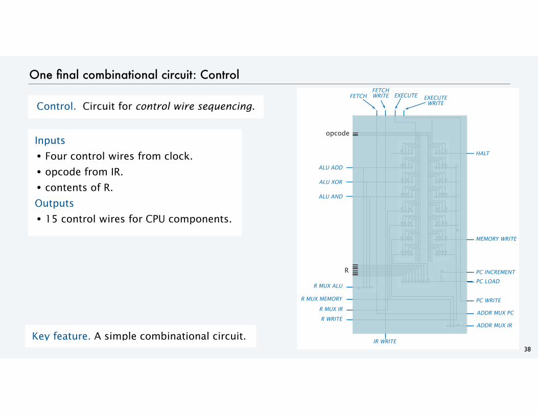
One final combinational circuit: Control
Control. Circuit for control wire sequencing.
Inputs
• Four control wires from clock.
• opcode from IR.
• contents of R. Outputs
• 15 control wires for CPU components.
Key feature. A simple combinational circuit.
ALU ADD
ALU XOR
ALU AND
R MUX ALU
R MUX MEMORY
R MUX IR
R WRITE
IR WRITE
MEMORY WRITE
PC LOAD
PC WRITE
PC INCREMENT
ADDR MUX PC
ADDR MUX IR
FETCHFETCHWRITE EXECUTE EXECUTE
WRITE
HALT
opcode
R
39
Control wire sequences
instruction EXECUTE EXECUTE WRITE
halt HALT
addALU ADD
R WRITER MUX ALU
xorALU ADD
R WRITER MUX ALU
andALU ADD
R WRITER MUX ALU
load address R MUX IR R WRITE
loadR MUX MEMORY R WRITE
ADDR MUX IR
store ADDR MUX IR MEMORY WRITE
FETCH FETCH WRITE EXECUTE WRITE
all instructions
ADDR MUX PCIR WRITE PC WRITE
PC INCREMENT*
* PC LOAD for branch if 0 if R is 0.
ALU ADD
ALU XOR
ALU AND
R MUX ALU
R MUX MEMORY
R MUX IR
R WRITE
IR WRITE
MEMORY WRITE
PC LOAD
PC WRITE
PC INCREMENT
ADDR MUX PC
ADDR MUX IR
FETCHFETCHWRITE EXECUTE EXECUTE
WRITE
HALT
opcode
R
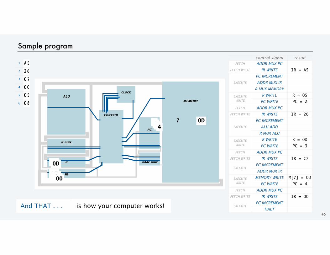
Sample program
40
And THAT . . . is how your computer works!
CLOCK
MEMORYALU
R
IR
PC
CONTROL
R mux
addr mux
`
`
`
control signal resultFETCH ADDR MUX PC
FETCH WRITE IR WRITE IR = A5
EXECUTE
PC INCREMENT
ADDR MUX IR
R MUX MEMORY
EXECUTE WRITE
R WRITE R = 05PC WRITE PC = 2
FETCH ADDR MUX PC
FETCH WRITE IR WRITE IR = 26
EXECUTE
PC INCREMENT
ALU ADD
R MUX ALU
EXECUTE WRITE
R WRITE R = 0DPC WRITE PC = 3
FETCH ADDR MUX PC
FETCH WRITE IR WRITE IR = C7
EXECUTEPC INCREMENT
ADDR MUX IR
EXECUTE WRITE
MEMORY WRITE M[7] = 0DPC WRITE PC = 4
FETCH ADDR MUX PC
FETCH WRITE IR WRITE IR = 00
EXECUTEPC INCREMENT
HALT
1 A5
2 26
3 C7
4 00
5 05
6 08
A5
05
1
26
2
0D
3
C7
0D74
00
R WRITE
IR WRITE
PC WRITE
MEMORY WRITE
PC INCREMENT
PC LOAD
ALU ADD
ALU XOR
ALU AND
ADDR MUX IR
ADDR MUX PC
R MUX ALU
R MUX MEM
R MUX IR
CONTROL
PC
MEMORY
R
IR
ALU FETCH
FETCH WRITEEXECUTE
EXECUTE WRITE
RUN
HALT
CLOCK
TOY-8 CPU
41
MEMORY
ALU
R
IR
PC
CONTROL
R MUX 3-way
addr MUX 2-way
CLOCK
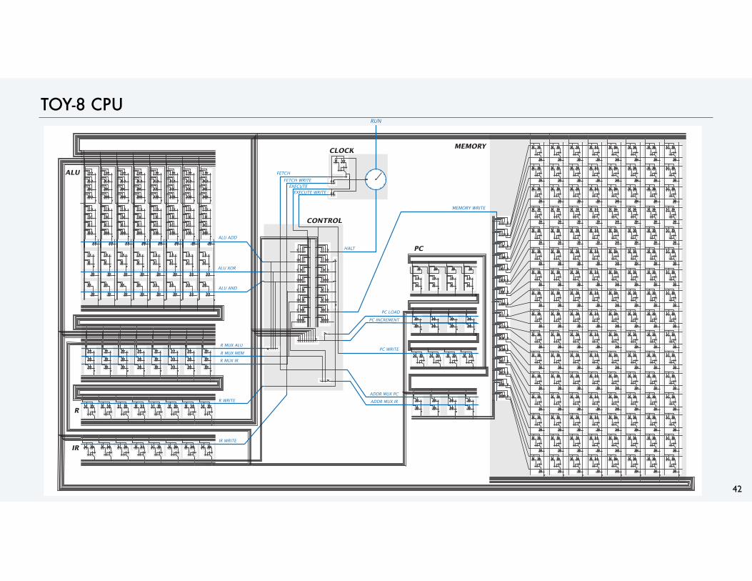
TOY-8 CPU
42
R WRITE
IR WRITE
PC WRITE
MEMORY WRITE
PC INCREMENT
PC LOAD
ALU ADD
ALU XOR
ALU AND
ADDR MUX IR
ADDR MUX PC
R MUX ALU
R MUX MEM
R MUX IR
CONTROL
PC
MEMORY
R
IR
ALU FETCH
FETCH WRITEEXECUTE
EXECUTE WRITE
RUN
HALT
CLOCK
43
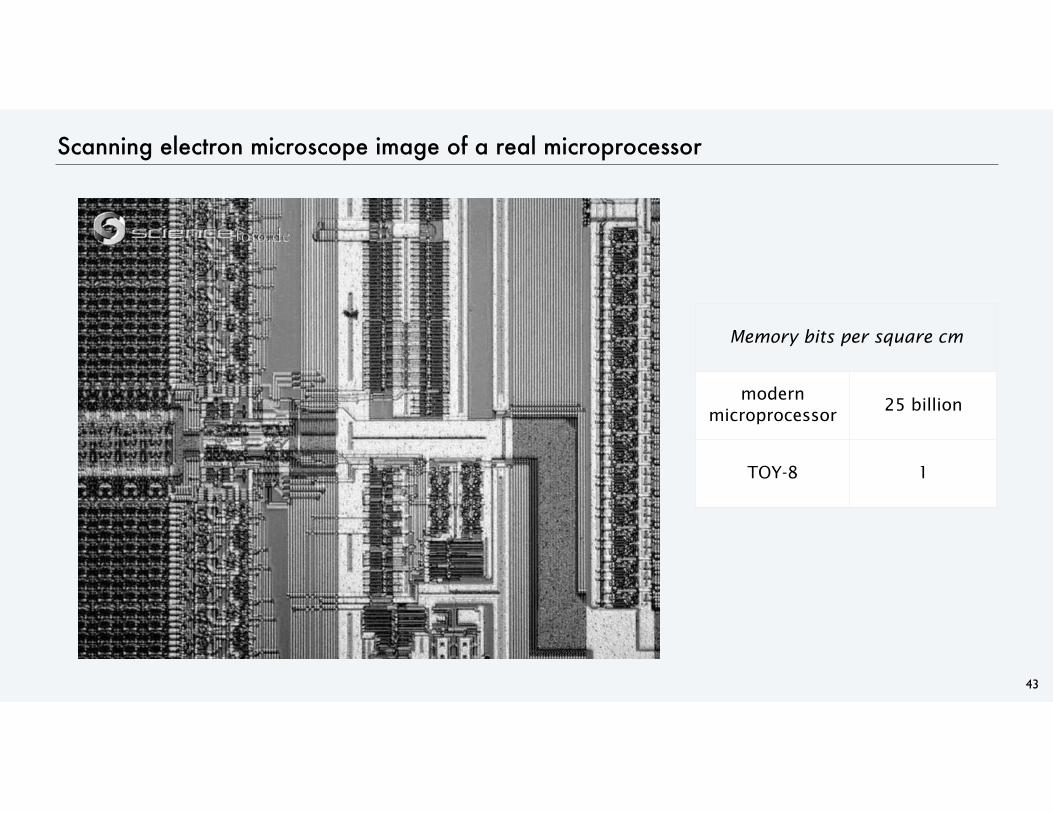
Scanning electron microscope image of a real microprocessor
Memory bits per square cm
modern microprocessor 25 billion
TOY-8 1
44
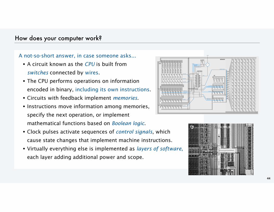
How does your computer work?
A not-so-short answer, in case someone asks...
• A circuit known as the CPU is built from switches connected by wires.
• The CPU performs operations on informationencoded in binary, including its own instructions.
• Circuits with feedback implement memories.
• Instructions move information among memories,specify the next operation, or implementmathematical functions based on Boolean logic.
• Clock pulses activate sequences of control signals, which cause state changes that implement machine instructions.
• Virtually everything else is implemented as layers of software, each layer adding additional power and scope.
R WRITE
IR WRITE
PC WRITE
MEMORY WRITE
PC INCREMENT
PC LOAD
ALU ADD
ALU XOR
ALU AND
ADDR MUX IR
ADDR MUX PC
R MUX ALU
R MUX MEM
R MUX IR
CONTROL
PC
MEMORY
R
IR
ALU FETCH
FETCH WRITEEXECUTE
EXECUTE WRITE
RUN
HALT
CLOCK
45
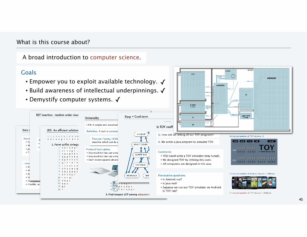
What is this course about?
Goals
• Empower you to exploit available technology.
• Build awareness of intellectual underpinnings.
• Demystify computer systems.
A broad introduction to computer science.
✓✓
✓

46
What is this course about?
Goals
• Empower you to exploit available technology.
• Build awareness of intellectual underpinnings.
• Demystify computer systems.
A broad introduction to computer science.
R O B E R T S E D G E W I C K K E V I N W A Y N E
Com
puter Science
ComputerScience
An Interdisciplinary Approach
✓✓
✓ Next: Algorithms.
AlgorithmsF O U R T H E D I T I O N
R O B E R T S E D G E W I C K K E V I N W A Y N E
C O M P U T E R S C I E N C E S E D G E W I C K / W A Y N E
CS.20.D.CPU.Components
Image sources http://download.intel.com/pressroom/images/corefamily/Westmere4.jpg
http://www.sciencefoto.de/detail.php?rubrik=Nano&id=214956&lang=en&q=&qrubrik=

http://introcs.cs.princeton.edu
R O B E R T S E D G E W I C K K E V I N W A Y N E
Com
puter Science
ComputerScience
An Interdisciplinary Approach
20. Central Processing Unit
COMPUTER SC I ENCE S E D G E W I C K / W A Y N E
PART I I : ALGORITHMS, MAC HINES , and THEORY
Sections 6.3−4