Embed Size (px)
Citation preview
1/33
XC6501 200mA High Speed LDO Regulator, Output Capacitor-Less, Low Power Consumption
GENERAL DESCRIPTION The XC6501 series is a high speed, low noise CMOS LDO regulator that can provide stable output voltages even without a load capacitor CL. This is possible because phase compensation is carried out internally unlike other LDOs where it is done externally. The series consists of a reference voltage source, driver transistor, error amplifier, current limit circuit, and phase compensation circuit. The CE function enables the circuit to be put into stand-by mode by inputting a low level signal to the CE pin thereby reducing current consumption from an already low 13μA (in operation) to less than 0.1μA. In the stand-by mode, if a CL capacitor is used, the electric charge stored at CL can be discharged via the internal auto-discharge switch and as a result, the VOUT pin quickly returns to the VSS level. The current limit fold-back circuit operates as a short circuit protection and a current limiter function for the output pin.
APPLICATIONS
Smart phones / Mobile phones
Portable games
Modules (wireless, cameras,etc.) Bluetooth
Digital-TV tuners
FEATURES Maximum Output Current : 200mA
Operating Voltage Range : 1.4~6.0V
Output Voltage Range
: 2.0~5.0V (±1%) (*1)
1.2~1.95V (±0.02V) (*1)
Dropout Voltage : 150mV@IOUT=100mA, VOUT=2.8V
Low Power Supply : 13μA @VOUT=2.8V
Stand-by Current : Less than 0.1μA
Ripple Rejection : 50dB@f=1kHz,VOUT=2.8V
Protection Circuits : Current limit (300mA, TYP.)
Short circuit protection
Output capacitor is not required : Internal phase compensation
CL High Speed Auto Discharge
Operating Ambient Temperature : -40~+85
Packages : SOT-25, SSOT-24, USP-4, USPN-4,USP-3, WLP-4-01
Environmentally Friendly : EU RoHS Compliant, Pb Free (*1) WLP-4-01 : 2.0~5.0V(±2%), 1.2~1.95V(±0.03V)
TYPICAL PERFORMANCE CHARACTERISTICS
XC6501 Series
2.0
2.2
2.4
2.6
2.8
3.0
3.2
Time (40μs/div)
Out
put V
olta
ge: V
OU
T(V
)
0
50
100
150
200
250
300
Out
put C
urre
nt: I
OU
T(m
A)CL=1.0μF
Output Current
CL無し
Ta=25,tr=tf=5μsCIN=0.1μF (ceramic)
XC6501 Series
2.0
2.2
2.4
2.6
2.8
3.0
3.2
Time (40μs/div)
Out
put V
olta
ge: V
OU
T(V
)
0
50
100
150
200
250
300
Out
put C
urre
nt: I
OU
T(m
A)CL=1.0μF
Output Current
CL無し
Ta=25,tr=tf=5μsCIN=0.1μF (ceramic)
Without CL
ETR03037-011
TYPICAL APPLICATION CIRCUIT
2/33
XC6501 Series BLOCK DIAGRAMS
*図のダイオードは、静電保護用のダイオードと寄生ダイオードです。
*Diodes inside the circuit are an ESD protection diode and a parasitic diode.
1) XC6501 Series A type
3) XC6501 Series C type
2) XC6501 Series B type
5) XC6501 Series P type
4) XC6501 Series D type
3/33
XC6501Series
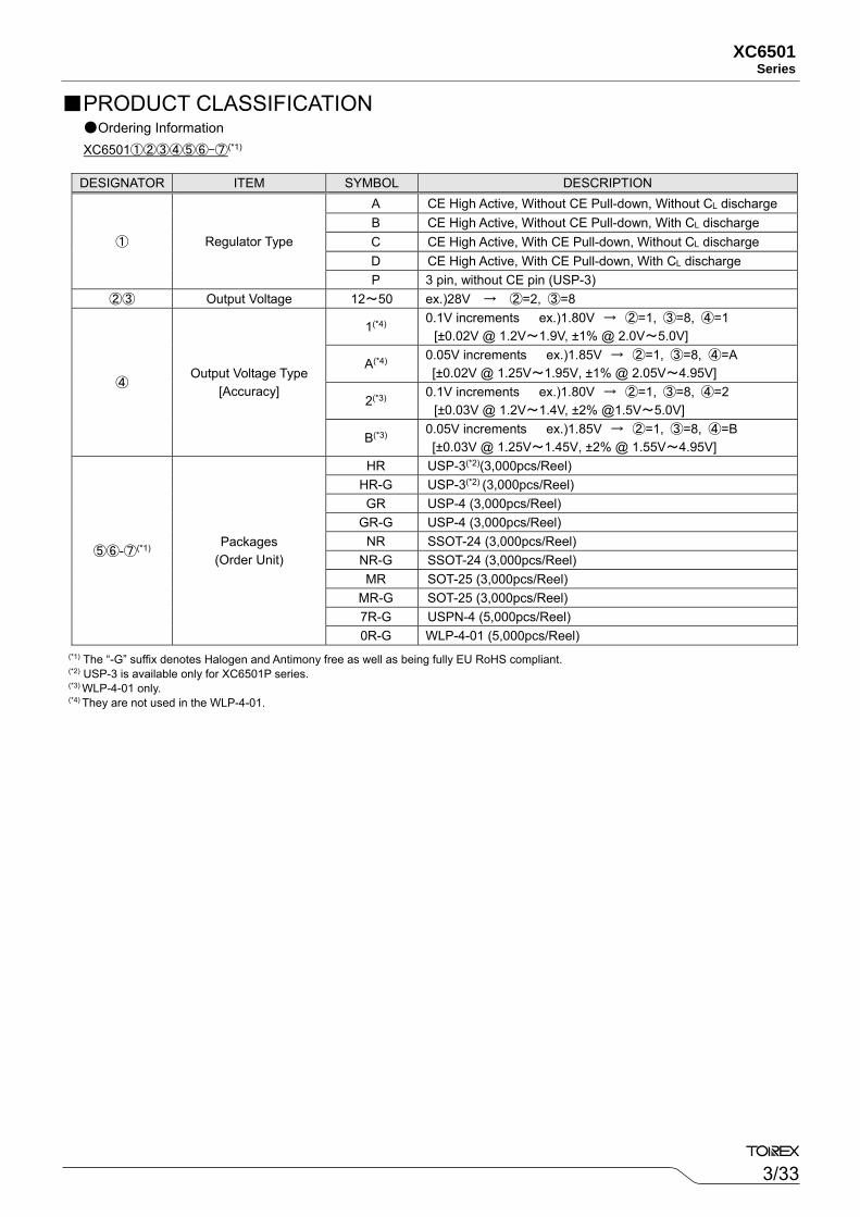
PRODUCT CLASSIFICATION Ordering Information XC6501①②③④⑤⑥-⑦(*1)
DESIGNATOR ITEM SYMBOL DESCRIPTION
① Regulator Type
A CE High Active, Without CE Pull-down, Without CL discharge B CE High Active, Without CE Pull-down, With CL discharge C CE High Active, With CE Pull-down, Without CL discharge D CE High Active, With CE Pull-down, With CL discharge P 3 pin, without CE pin (USP-3)
②③ Output Voltage 12~50 ex.)28V → ②=2, ③=8
④ Output Voltage Type
[Accuracy]
1(*4) 0.1V increments ex.)1.80V → ②=1, ③=8, ④=1
[±0.02V @ 1.2V~1.9V, ±1% @ 2.0V~5.0V]
A(*4) 0.05V increments ex.)1.85V → ②=1, ③=8, ④=A [±0.02V @ 1.25V~1.95V, ±1% @ 2.05V~4.95V]
2(*3) 0.1V increments ex.)1.80V → ②=1, ③=8, ④=2
[±0.03V @ 1.2V~1.4V, ±2% @1.5V~5.0V]
B(*3) 0.05V increments ex.)1.85V → ②=1, ③=8, ④=B [±0.03V @ 1.25V~1.45V, ±2% @ 1.55V~4.95V]
⑤⑥-⑦(*1) Packages
(Order Unit)
HR USP-3(*2)(3,000pcs/Reel) HR-G USP-3(*2) (3,000pcs/Reel) GR USP-4 (3,000pcs/Reel)
GR-G USP-4 (3,000pcs/Reel) NR SSOT-24 (3,000pcs/Reel)
NR-G SSOT-24 (3,000pcs/Reel) MR SOT-25 (3,000pcs/Reel)
MR-G SOT-25 (3,000pcs/Reel) 7R-G USPN-4 (5,000pcs/Reel) 0R-G WLP-4-01 (5,000pcs/Reel)
(*1) The “-G” suffix denotes Halogen and Antimony free as well as being fully EU RoHS compliant. (*2) USP-3 is available only for XC6501P series. (*3) WLP-4-01 only. (*4) They are not used in the WLP-4-01.
4/33
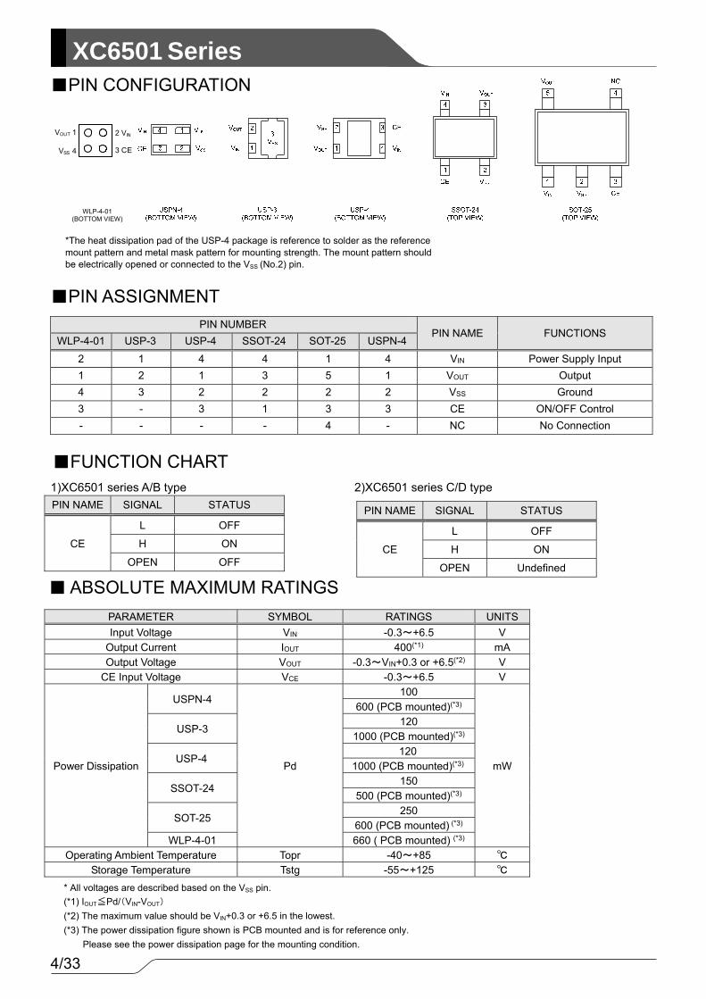
XC6501 Series PIN CONFIGURATION
PIN ASSIGNMENT
FUNCTION CHART
1)XC6501 series A/B type 2)XC6501 series C/D type PIN NAME SIGNAL STATUS
CE
L OFF
H ON
OPEN OFF
ABSOLUTE MAXIMUM RATINGS
PIN NUMBER PIN NAME FUNCTIONS
WLP-4-01 USP-3 USP-4 SSOT-24 SOT-25 USPN-4
2 1 4 4 1 4 VIN Power Supply Input 1 2 1 3 5 1 VOUT Output 4 3 2 2 2 2 VSS Ground 3 - 3 1 3 3 CE ON/OFF Control - - - - 4 - NC No Connection
PIN NAME SIGNAL STATUS
CE
L OFF
H ON
OPEN Undefined
PARAMETER SYMBOL RATINGS UNITS Input Voltage VIN -0.3~+6.5 V
Output Current IOUT 400(*1) mA Output Voltage VOUT -0.3~VIN+0.3 or +6.5(*2) V
CE Input Voltage VCE -0.3~+6.5 V
Power Dissipation
USPN-4
Pd
100
mW
600 (PCB mounted)(*3)
USP-3 120
1000 (PCB mounted)(*3)
USP-4 120
1000 (PCB mounted)(*3)
SSOT-24 150
500 (PCB mounted)(*3)
SOT-25 250
600 (PCB mounted) (*3) WLP-4-01 660 ( PCB mounted) (*3)
Operating Ambient Temperature Topr -40~+85
Storage Temperature Tstg -55~+125
*The heat dissipation pad of the USP-4 package is reference to solder as the reference mount pattern and metal mask pattern for mounting strength. The mount pattern should be electrically opened or connected to the VSS (No.2) pin.
* All voltages are described based on the VSS pin. (*1) IOUT≦Pd/(VIN-VOUT) (*2) The maximum value should be VIN+0.3 or +6.5 in the lowest. (*3) The power dissipation figure shown is PCB mounted and is for reference only.
Please see the power dissipation page for the mounting condition.
2 VIN
3 CE
VOUT 1
VSS 4
WLP-4-01 (BOTTOM VIEW)
5/33
XC6501Series
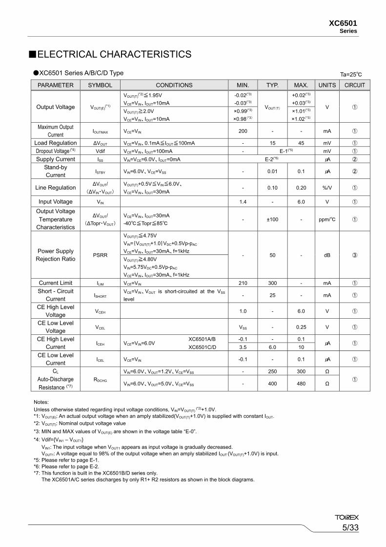
ELECTRICAL CHARACTERISTICS
XC6501 Series A/B/C/D Type
PARAMETER SYMBOL CONDITIONS MIN. TYP. MAX. UNITS CIRCUIT
Output Voltage VOUT(E)(*1)
VOUT(T)(*2)≦1.95V
VCE=VIN、IOUT=10mA -0.02(*3)
-0.03(*3) VOUT(T)
+0.02(*3)
+0.03(*3) V ①
VOUT(T)≧2.0V VCE=VIN、IOUT=10mA
×0.99(*3)
×0.98(*3)
×1.01(*3)
×1.02(*3) Maximum Output
Current IOUTMAX VCE=VIN 200 - - mA ①
Load Regulation ∆VOUT VCE=VIN、0.1mA≦IOUT≦100mA - 15 45 mV ①
Dropout Voltage (*4) Vdif VCE=VIN、IOUT=100mA - E-1(*5) mV ①
Supply Current ISS VIN=VCE=6.0V、IOUT=0mA E-2(*6) μA ②
Stand-by Current
ISTBY VIN=6.0V、VCE=VSS - 0.01 0.1 μA ②
Line Regulation ∆VOUT/
(∆VIN・VOUT) VOUT(T)+0.5V≦VIN≦6.0V、 VCE=VIN、IOUT=30mA
- 0.10 0.20 %/V ①
Input Voltage VIN 1.4 - 6.0 V ①
Output Voltage Temperature
Characteristics
∆VOUT/ (∆Topr・VOUT)
VCE=VIN、IOUT=30mA -40≦Topr≦85
- ±100 - ppm/ ①
Power Supply Rejection Ratio
PSRR
VOUT(T)≦4.75V VIN={VOUT(T)+1.0}VDC+0.5Vp-pAC VCE=VIN、IOUT=30mA、f=1kHz
- 50 - dB ③ VOUT(T)≧4.80V VIN=5.75VDC+0.5Vp-pAC VCE=VIN、IOUT=30mA、f=1kHz
Current Limit ILIM VCE=VIN 210 300 - mA ①
Short - Circuit Current
ISHORT VCE=VIN、VOUT is short-circuited at the VSS level
- 25 - mA ①
CE High Level Voltage
VCEH 1.0 - 6.0 V ①
CE Low Level Voltage
VCEL VSS - 0.25 V ①
CE High Level Current
ICEH VCE=VIN=6.0V XC6501A/B -0.1 - 0.1
μA ① XC6501C/D 3.5 6.0 10
CE Low Level Current
ICEL VCE=VIN -0.1 - 0.1 μA ①
CL
Auto-Discharge Resistance (*7)
RDCHG VIN=6.0V、VOUT=1.2V、VCE=VSS - 250 300 Ω
① VIN=6.0V、VOUT=5.0V、VCE=VSS - 400 480 Ω
Notes: Unless otherwise stated regarding input voltage conditions, VIN=VOUT(T)
(*2)+1.0V. *1: VOUT(E): An actual output voltage when an amply stabilized(VOUT(T)+1.0V) is supplied with constant IOUT. *2: VOUT(T): Nominal output voltage value *3: MIN and MAX values of VOUT(E) are shown in the voltage table “E-0”. *4: Vdif=VIN1 – VOUT1
VIN1: The input voltage when VOUT1 appears as input voltage is gradually decreased. VOUT1: A voltage equal to 98% of the output voltage when an amply stabilized IOUT (VOUT(T)+1.0V) is input.
*5: Please refer to page E-1. *6: Please refer to page E-2. *7: This function is built in the XC6501B/D series only.
The XC6501A/C series discharges by only R1+ R2 resistors as shown in the block diagrams.
Ta=25
6/33
XC6501 Series
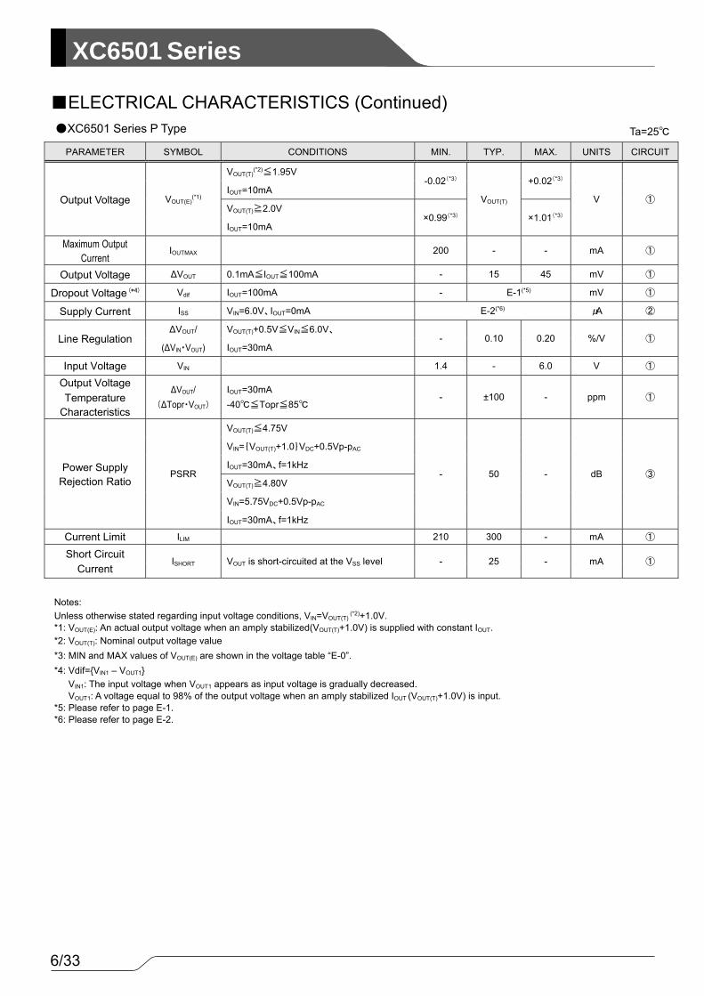
ELECTRICAL CHARACTERISTICS (Continued)
PARAMETER SYMBOL CONDITIONS MIN. TYP. MAX. UNITS CIRCUIT
Output Voltage VOUT(E)(*1)
VOUT(T)(*2)≦1.95V
-0.02(*3)
VOUT(T)
+0.02(*3)
V ① IOUT=10mA
VOUT(T)≧2.0V ×0.99(*3) ×1.01(*3)
IOUT=10mA
Maximum Output Current
IOUTMAX 200 - - mA ①
Output Voltage ∆VOUT 0.1mA≦IOUT≦100mA - 15 45 mV ①
Dropout Voltage (*4) Vdif IOUT=100mA - E-1(*5) mV ①
Supply Current ISS VIN=6.0V、IOUT=0mA E-2(*6) μA ②
Line Regulation ∆VOUT/ VOUT(T)+0.5V≦VIN≦6.0V、
- 0.10 0.20 %/V ① (∆VIN・VOUT) IOUT=30mA
Input Voltage VIN 1.4 - 6.0 V ①
Output Voltage Temperature
Characteristics
∆VOUT/ (∆Topr・VOUT)
IOUT=30mA -40≦Topr≦85
- ±100 - ppm ①
Power Supply Rejection Ratio
PSRR
VOUT(T)≦4.75V
- 50 - dB ③
VIN={VOUT(T)+1.0}VDC+0.5Vp-pAC
IOUT=30mA、f=1kHz
VOUT(T)≧4.80V
VIN=5.75VDC+0.5Vp-pAC
IOUT=30mA、f=1kHz
Current Limit ILIM 210 300 - mA ①
Short Circuit Current
ISHORT VOUT is short-circuited at the VSS level - 25 - mA ①
Ta=25 XC6501 Series P Type
Notes: Unless otherwise stated regarding input voltage conditions, VIN=VOUT(T)
(*2)+1.0V. *1: VOUT(E): An actual output voltage when an amply stabilized(VOUT(T)+1.0V) is supplied with constant IOUT. *2: VOUT(T): Nominal output voltage value *3: MIN and MAX values of VOUT(E) are shown in the voltage table “E-0”. *4: Vdif=VIN1 – VOUT1
VIN1: The input voltage when VOUT1 appears as input voltage is gradually decreased. VOUT1: A voltage equal to 98% of the output voltage when an amply stabilized IOUT (VOUT(T)+1.0V) is input.
*5: Please refer to page E-1. *6: Please refer to page E-2.
7/33
XC6501Series
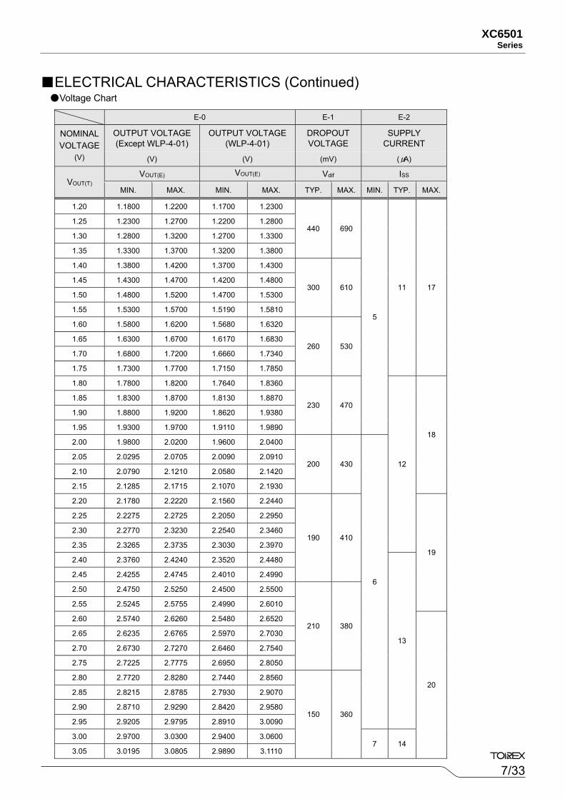
ELECTRICAL CHARACTERISTICS (Continued) Voltage Chart
E-0 E-1 E-2
NOMINAL VOLTAGE
(V)
OUTPUT VOLTAGE (Except WLP-4-01)
OUTPUT VOLTAGE (WLP-4-01)
DROPOUT VOLTAGE
SUPPLY CURRENT
(V) (V) (mV) (μA)
VOUT(T) VOUT(E) VOUT(E) Vdif ISS
MIN. MAX. MIN. MAX. TYP. MAX. MIN. TYP. MAX.
1.20 1.1800 1.2200 1.1700 1.2300
440 690
5
11 17
1.25 1.2300 1.2700 1.2200 1.2800
1.30 1.2800 1.3200 1.2700 1.3300
1.35 1.3300 1.3700 1.3200 1.3800
1.40 1.3800 1.4200 1.3700 1.4300
300 6101.45 1.4300 1.4700 1.4200 1.4800
1.50 1.4800 1.5200 1.4700 1.5300
1.55 1.5300 1.5700 1.5190 1.5810
1.60 1.5800 1.6200 1.5680 1.6320
260 5301.65 1.6300 1.6700 1.6170 1.6830
1.70 1.6800 1.7200 1.6660 1.7340
1.75 1.7300 1.7700 1.7150 1.7850
1.80 1.7800 1.8200 1.7640 1.8360
230 470
12
18
1.85 1.8300 1.8700 1.8130 1.8870
1.90 1.8800 1.9200 1.8620 1.9380
1.95 1.9300 1.9700 1.9110 1.9890
2.00 1.9800 2.0200 1.9600 2.0400
200 430
6
2.05 2.0295 2.0705 2.0090 2.0910
2.10 2.0790 2.1210 2.0580 2.1420
2.15 2.1285 2.1715 2.1070 2.1930
2.20 2.1780 2.2220 2.1560 2.2440
190 410
19
2.25 2.2275 2.2725 2.2050 2.2950
2.30 2.2770 2.3230 2.2540 2.3460
2.35 2.3265 2.3735 2.3030 2.3970
2.40 2.3760 2.4240 2.3520 2.4480
13
2.45 2.4255 2.4745 2.4010 2.4990
2.50 2.4750 2.5250 2.4500 2.5500
210 380
2.55 2.5245 2.5755 2.4990 2.6010
2.60 2.5740 2.6260 2.5480 2.6520
20
2.65 2.6235 2.6765 2.5970 2.7030
2.70 2.6730 2.7270 2.6460 2.7540
2.75 2.7225 2.7775 2.6950 2.8050
2.80 2.7720 2.8280 2.7440 2.8560
150 360
2.85 2.8215 2.8785 2.7930 2.9070
2.90 2.8710 2.9290 2.8420 2.9580
2.95 2.9205 2.9795 2.8910 3.0090
3.00 2.9700 3.0300 2.9400 3.0600 7 14
3.05 3.0195 3.0805 2.9890 3.1110
8/33
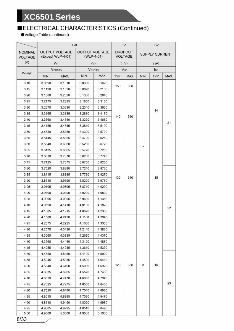
XC6501 Series ELECTRICAL CHARACTERISTICS (Continued) Voltage Table (continued)
E-0 E-1 E-2
NOMINAL VOLTAGE
(V)
OUTPUT VOLTAGE(Except WLP-4-01)
OUTPUT VOLTAGE(WLP-4-01)
DROPOUT VOLTAGE SUPPLY CURRENT
(V) (V) (mV) (μA)
VOUT(T) VOUT(E) VOUT(E) Vdif ISS
MIN. MAX. MIN. MAX. TYP. MAX. MIN. TYP. MAX.
3.10 3.0690 3.1310 3.0380 3.1620 150 360
7
14
21
3.15 3.1190 3.1820 3.0870 3.2130
3.20 3.1680 3.2320 3.1360 3.2640
140 350
3.25 3.2175 3.2825 3.1850 3.3150
3.30 3.2670 3.3330 3.2340 3.3660
3.35 3.3165 3.3835 3.2830 3.4170
3.40 3.3660 3.4340 3.3320 3.4680
3.45 3.4155 3.4845 3.3810 3.5190
3.50 3.4650 3.5350 3.4300 3.5700
3.55 3.5145 3.5855 3.4790 3.6210
3.60 3.5640 3.6360 3.5280 3.6720
130 340 15
3.65 3.6135 3.6865 3.5770 3.7230
3.70 3.6630 3.7370 3.6260 3.7740
3.75 3.7125 3.7875 3.6750 3.8250
3.80 3.7620 3.8380 3.7240 3.8760
22
3.85 3.8115 3.8885 3.7730 3.9270
3.90 3.8610 3.9390 3.8220 3.9780
3.95 3.9105 3.9895 3.8710 4.0290
4.00 3.9600 4.0400 3.9200 4.0800
4.05 4.0095 4.0905 3.9690 4.1310
4.10 4.0590 4.1410 4.0180 4.1820
4.15 4.1085 4.1915 4.0670 4.2330
4.20 4.1580 4.2420 4.1160 4.2840
120 330 8 16
4.25 4.2075 4.2925 4.1650 4.3350
4.30 4.2570 4.3430 4.2140 4.3860
4.35 4.3065 4.3935 4.2630 4.4370
4.40 4.3560 4.4440 4.3120 4.4880
4.45 4.4055 4.4945 4.3610 4.5390
4.50 4.4550 4.5450 4.4100 4.5900
23
4.55 4.5045 4.5955 4.4590 4.6410
4.60 4.5540 4.6460 4.5080 4.6920
4.65 4.6035 4.6965 4.5570 4.7430
4.70 4.6530 4.7470 4.6060 4.7940
4.75 4.7025 4.7975 4.6550 4.8450
4.80 4.7520 4.8480 4.7040 4.8960
4.85 4.8015 4.8985 4.7530 4.9470
4.90 4.8510 4.9490 4.8020 4.9980
4.95 4.9005 4.9995 4.8510 5.0490 5.00 4.9500 5.0500 4.9000 5.1000
9/33
XC6501Series
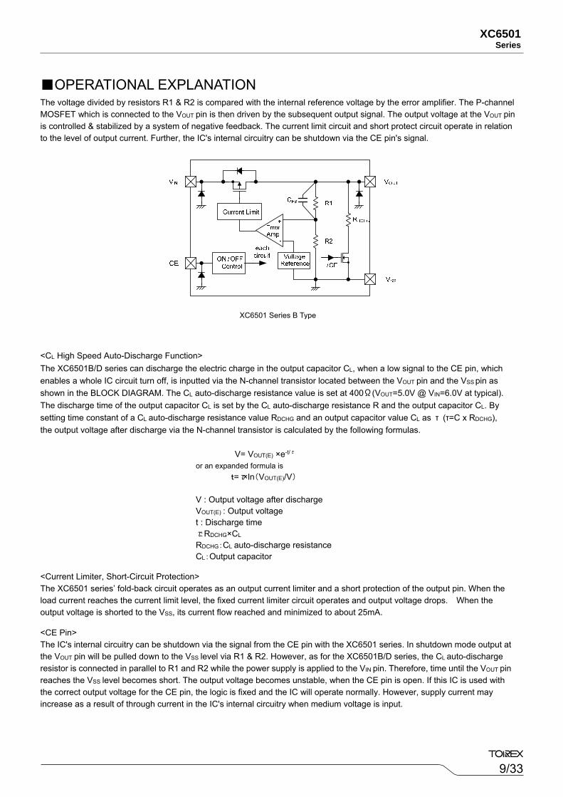
OPERATIONAL EXPLANATION The voltage divided by resistors R1 & R2 is compared with the internal reference voltage by the error amplifier. The P-channel MOSFET which is connected to the VOUT pin is then driven by the subsequent output signal. The output voltage at the VOUT pin is controlled & stabilized by a system of negative feedback. The current limit circuit and short protect circuit operate in relation to the level of output current. Further, the IC's internal circuitry can be shutdown via the CE pin's signal.
<CL High Speed Auto-Discharge Function> The XC6501B/D series can discharge the electric charge in the output capacitor CL, when a low signal to the CE pin, which enables a whole IC circuit turn off, is inputted via the N-channel transistor located between the VOUT pin and the VSS pin as shown in the BLOCK DIAGRAM. The CL auto-discharge resistance value is set at 400Ω(VOUT=5.0V @ VIN=6.0V at typical). The discharge time of the output capacitor CL is set by the CL auto-discharge resistance R and the output capacitor CL. By setting time constant of a CL auto-discharge resistance value RDCHG and an output capacitor value CL as τ (τ=C x RDCHG), the output voltage after discharge via the N-channel transistor is calculated by the following formulas.
<Current Limiter, Short-Circuit Protection> The XC6501 series’ fold-back circuit operates as an output current limiter and a short protection of the output pin. When the load current reaches the current limit level, the fixed current limiter circuit operates and output voltage drops. When the output voltage is shorted to the VSS, its current flow reached and minimized to about 25mA.
<CE Pin> The IC's internal circuitry can be shutdown via the signal from the CE pin with the XC6501 series. In shutdown mode output at the VOUT pin will be pulled down to the VSS level via R1 & R2. However, as for the XC6501B/D series, the CL auto-discharge resistor is connected in parallel to R1 and R2 while the power supply is applied to the VIN pin. Therefore, time until the VOUT pin reaches the VSS level becomes short. The output voltage becomes unstable, when the CE pin is open. If this IC is used with the correct output voltage for the CE pin, the logic is fixed and the IC will operate normally. However, supply current may increase as a result of through current in the IC's internal circuitry when medium voltage is input.
V= VOUT(E) ×e-t/τ
or an expanded formula is t=τ×ln(VOUT(E)/V)
V : Output voltage after discharge
VOUT(E) : Output voltage
t : Discharge time τ:RDCHG×CL RDCHG:CL auto-discharge resistance
CL:Output capacitor
XC6501 Series B Type
10/33
XC6501 Series
NOTES ON USE
1. Please use this IC within the stated absolute maximum ratings. The IC is liable to malfunction should the ratings be exceeded.
2. This IC achieves stable operation without an output capacitor CL by internal phase compensation. However, wiring impedance is high, operations may become unstable due to noise and/or phase lag depending on output current. Please wire the input capacitor CIN and the output capacitor CL as close to the IC as possible.
3. Torex places an importance on improving our products and their reliability. We request that users incorporate fail-safe designs and post-aging protection treatment when using Torex products in their systems.
11/33
XC6501Series
TEST CIRCUITS
The CE pin does not exist in the XC6501 series P type, please disregard CE description in above test circuit.
測定回路①
測定回路②
測定回路③
V
CE
VIN
VSS
VOUT
V
A
CIN=0.1μF(ceramic) IOUT
AV
CE
VIN
VSS
VOUT
A
V
CE
VIN
VSS
VOUT
VA
IOUT
V
Circuit ②
Circuit ③
Circuit ①
12/33
XC6501 Series
(1) Output Voltage vs. Output Current
Ta = 25
CIN = 0.1μF (ceramic)
Ta = 25CIN = 0.1μF (ceramic)
Ta = 25CIN = 0.1μF (ceramic)
VIN = 6.0V
CIN = 0.1μF (ceramic)
VIN = 3.8V
CIN = 0.1μF (ceramic)
VIN = 2.2V
CIN = 0.1μF (ceramic)
XC6501x121
0.0
0.3
0.6
0.9
1.2
1.5
0 50 100 150 200 250 300 350 400
Output Current: IOUT [mA]
Outp
ut
Voltag
e: V
OU
T [
V]
Ta = -40
Ta = 25
Ta = 85
XC6501x501
0.0
1.0
2.0
3.0
4.0
5.0
6.0
0 50 100 150 200 250 300 350 400
Output Current: IOUT [mA]
Outp
ut
Voltag
e: V
OU
T [
V]
Ta = -40
Ta = 25
Ta = 85
XC6501x281
0.0
0.5
1.0
1.5
2.0
2.5
3.0
0 50 100 150 200 250 300 350 400
Output Current: IOUT [mA]
Outp
ut
Voltag
e: V
OU
T [
V]
Ta = -40
Ta = 25
Ta = 85
XC6501x501
0.0
1.0
2.0
3.0
4.0
5.0
6.0
0 50 100 150 200 250 300 350 400
Output Current: IOUT [mA]
Outp
ut
Voltag
e: V
OU
T [
V]
XC6501x281
0.0
0.5
1.0
1.5
2.0
2.5
3.0
0 50 100 150 200 250 300 350 400
Output Current: IOUT [mA]
Outp
ut
Voltag
e: V
OU
T [
V]
XC6501x121
0.0
0.3
0.6
0.9
1.2
1.5
0 50 100 150 200 250 300 350 400
Output Current: IOUT [mA]O
utp
ut
Voltag
e: V
OU
T [
V]
VIN = 3.1V
VIN = 3.3V
VIN = 3.8V
VIN = 5.3V
VIN = 5.5V
VIN = 6.0V
VIN = 1.5V
VIN = 1.7V
VIN = 2.2V
*CE Voltage condition: Unless otherwise stated, VCE =VIN
TYPICAL PERFORMANCE CHARACTERISTICS
13/33
XC6501Series
(2) Output Voltage vs. Input Voltage
Ta = 25
CIN = 0.1μF (ceramic)
Ta = 25
CIN = 0.1μF (ceramic)
Ta = 25CIN = 0.1μF (ceramic)
Ta = 25CIN = 0.1μF (ceramic)
Ta = 25CIN = 0.1μF (ceramic)
Ta = 25CIN = 0.1μF (ceramic)
XC6501x281
2.74
2.76
2.78
2.80
2.82
2.84
2.86
3.2 3.9 4.6 5.3 6.0
Input Voltage: VIN [V]
Outp
ut
Voltag
e: V
OU
T [
V]
XC6501x121
1.14
1.16
1.18
1.20
1.22
1.24
1.26
2.0 3.0 4.0 5.0 6.0
Input Voltage: VIN [V]
Outp
ut
Voltag
e: V
OU
T [
V]
IOUT = 10mA
IOUT = 30mA
IOUT = 100mA
XC6501x121
0.4
0.6
0.8
1.0
1.2
1.4
0.5 1.0 1.5 2.0 2.5
Input Voltage: VIN [V]
Outp
ut
Voltag
e: V
OU
T [
V]
XC6501x281
2.0
2.2
2.4
2.6
2.8
3.0
2.0 2.5 3.0 3.5 4.0
Input Voltage: VIN [V]
Outp
ut
Voltag
e: V
OU
T [
V]
XC6501x501
4.2
4.4
4.6
4.8
5.0
5.2
4.0 4.5 5.0 5.5 6.0
Input Voltage: VIN [V]
Outp
ut
Voltag
e: V
OU
T [
V]
XC6501x501
4.94
4.96
4.98
5.00
5.02
5.04
5.06
5.2 5.4 5.6 5.8 6.0
Input Voltage: VIN [V]
Outp
ut
Voltag
e: V
OU
T [
V]
IOUT = 10mA
IOUT = 30mA
IOUT = 100mA
IOUT = 10mA
IOUT = 30mA
IOUT = 100mA
IOUT = 10mA
IOUT = 30mA
IOUT = 100mA
IOUT = 10mA
IOUT = 30mA
IOUT = 100mA
IOUT = 10mA
IOUT = 30mA
IOUT = 100mA
TYPICAL PERFORMANCE CHARACTERISTICS (Continued)
14/33
XC6501 Series
(3) Dropout Voltage vs. Output Current
(4) Supply Current vs. Input Voltage
CIN = 0.1μF (ceramic) CIN = 0.1μF (ceramic)
CIN = 0.1μF (ceramic)
XC6501x121
0.0
0.2
0.4
0.6
0.8
1.0
0 50 100 150 200
Output Current: IOUT [mA]
Dro
pout
Voltag
e: V
dif
[V] Ta = -40
Ta = 25
Ta = 85
XC6501x501
0.0
0.1
0.2
0.3
0.4
0.5
0 50 100 150 200
Output Current: IOUT [mA]
Dro
pout
Voltag
e: V
dif
[V] Ta = -40
Ta = 25
Ta = 85
XC6501x281
0.0
0.1
0.2
0.3
0.4
0.5
0 50 100 150 200
Output Current: IOUT [mA]
Dro
pout
Voltag
e: V
dif
[V] Ta = -40
Ta = 25
Ta = 85
XC6501x121
0.0
4.0
8.0
12.0
16.0
0 1 2 3 4 5 6
Input Voltage: VIN [V]
Supp
ly C
urr
ent: I S
S [
μA
]
Ta = -40
Ta = 25
Ta = 85
XC6501x281
0.0
4.0
8.0
12.0
16.0
0 1 2 3 4 5 6
Input Voltage: VIN [V]
Supp
ly C
urr
ent: I S
S [
μA
]
Ta = -40
Ta = 25
Ta = 85
XC6501x501
0.0
5.0
10.0
15.0
20.0
0 1 2 3 4 5 6
Input Voltage: VIN [V]
Supp
ly C
urr
ent: I S
S [
μA
]
Ta = -40
Ta = 25
Ta = 85
※Below the minimum operating voltage
TYPICAL PERFORMANCE CHARACTERISTICS (Continued)
15/33
XC6501Series
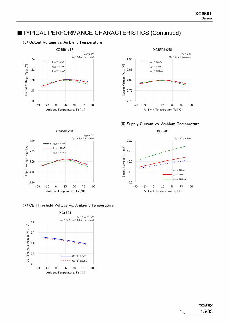
(5) Output Voltage vs. Ambient Temperature
(6) Supply Current vs. Ambient Temperature
(7) CE Threshold Voltage vs. Ambient Temperature
VIN = 3.8V
CIN = 0.1μF (ceramic)
VIN = 2.2V
CIN = 0.1μF (ceramic)
VIN = 6.0V
CIN = 0.1μF (ceramic)
VIN = VOUT + 1.0V
IOUT = 1mA, CIN = 0.1μF (ceramic)
VIN = VOUT + 1.0V
XC6501x121
1.16
1.18
1.20
1.22
1.24
-50 -25 0 25 50 75 100
Ambient Temperature: Ta []
Outp
ut
Voltag
e: V
OU
T [
V]
XC6501x281
2.70
2.75
2.80
2.85
2.90
-50 -25 0 25 50 75 100
Ambient Temperature: Ta []
Outp
ut
Voltag
e: V
OU
T [
V]
XC6501x501
4.90
4.95
5.00
5.05
5.10
-50 -25 0 25 50 75 100
Ambient Temperature: Ta []
Outp
ut
Voltag
e: V
OU
T [
V]
XC6501
0.0
5.0
10.0
15.0
20.0
-50 -25 0 25 50 75 100
Ambient Temperature: Ta []
Supp
ly C
urr
ent: I S
S [
μA
]
XC6501
0.4
0.5
0.6
0.7
0.8
-50 -25 0 25 50 75 100
Ambient Temperature: Ta []
CE T
hre
shold
Voltag
e: V
CE [
V]
CE "H" LEVEL
CE "L" LEVEL
IOUT = 10mA
IOUT = 30mA
IOUT = 100mA
IOUT = 10mA
IOUT = 30mA
IOUT = 100mA
IOUT = 10mA
IOUT = 30mA
IOUT = 100mA
IOUT = 10mA
IOUT = 30mA
IOUT = 100mA
TYPICAL PERFORMANCE CHARACTERISTICS (Continued)
16/33
XC6501 Series
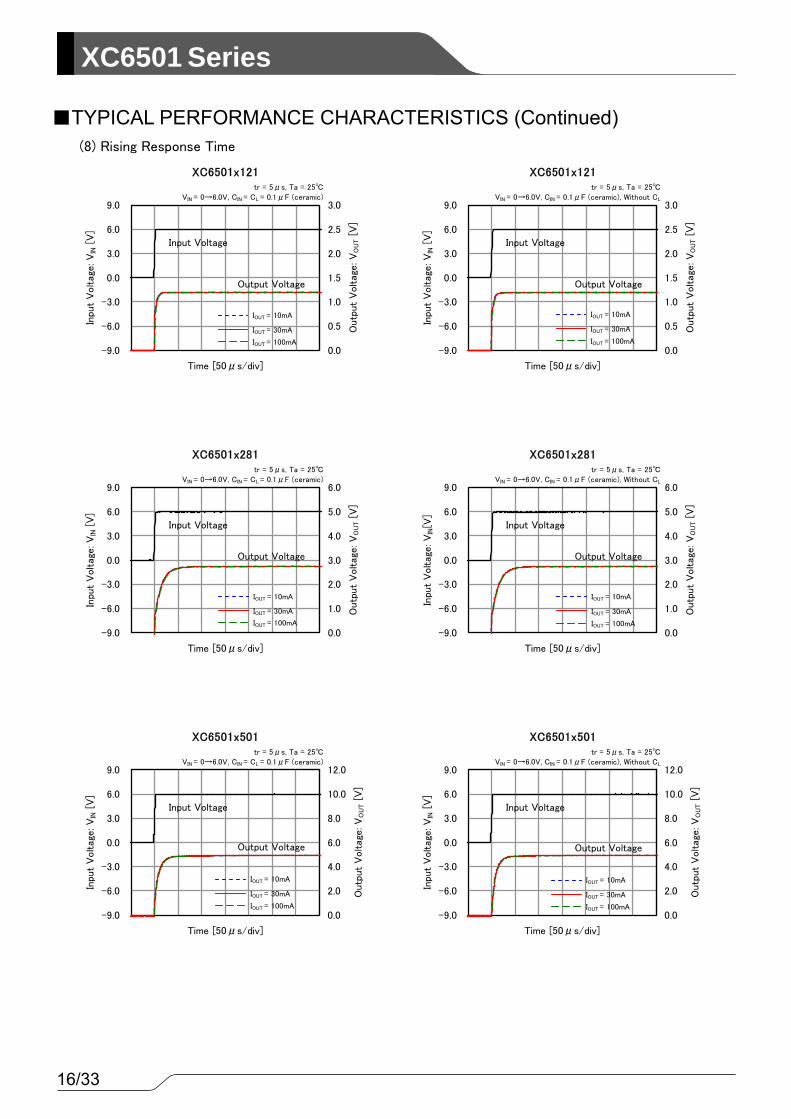
(8) Rising Response Time
tr = 5μs, Ta = 25
VIN = 0→6.0V, CIN = CL = 0.1μF (ceramic)
tr = 5μs, Ta = 25
VIN = 0→6.0V, CIN = 0.1μF (ceramic), Without CL
tr = 5μs, Ta = 25VIN = 0→6.0V, CIN = 0.1μF (ceramic), Without CL
tr = 5μs, Ta = 25VIN = 0→6.0V, CIN = CL = 0.1μF (ceramic)
tr = 5μs, Ta = 25VIN = 0→6.0V, CIN = 0.1μF (ceramic), Without CL
tr = 5μs, Ta = 25VIN = 0→6.0V, CIN = CL = 0.1μF (ceramic)
XC6501x501
-9.0
-6.0
-3.0
0.0
3.0
6.0
9.0
Time [50μs/div]
Inpu
t V
oltag
e: V
IN [
V]
0.0
2.0
4.0
6.0
8.0
10.0
12.0
Outp
ut
Voltag
e: V
OU
T [
V]
XC6501x501
-9.0
-6.0
-3.0
0.0
3.0
6.0
9.0
Time [50μs/div]
Inpu
t V
oltag
e: V
IN [
V]
0.0
2.0
4.0
6.0
8.0
10.0
12.0
Outp
ut
Voltag
e: V
OU
T [
V]
XC6501x281
-9.0
-6.0
-3.0
0.0
3.0
6.0
9.0
Time [50μs/div]
Inpu
t V
oltag
e: V
IN [
V]
0.0
1.0
2.0
3.0
4.0
5.0
6.0
Outp
ut
Voltag
e: V
OU
T [
V]
XC6501x281
-9.0
-6.0
-3.0
0.0
3.0
6.0
9.0
Time [50μs/div]
Inpu
t V
oltag
e: V
IN[V
]
0.0
1.0
2.0
3.0
4.0
5.0
6.0
Outp
ut
Voltag
e: V
OU
T [
V]
XC6501x121
-9.0
-6.0
-3.0
0.0
3.0
6.0
9.0
Time [50μs/div]
Inpu
t V
oltag
e: V
IN [
V]
0.0
0.5
1.0
1.5
2.0
2.5
3.0
Outp
ut
Voltag
e: V
OU
T [
V]
Input Voltage
Output Voltage
XC6501x121
-9.0
-6.0
-3.0
0.0
3.0
6.0
9.0
Time [50μs/div]
Inpu
t V
oltag
e: V
IN [
V]
0.0
0.5
1.0
1.5
2.0
2.5
3.0
Outp
ut
Voltag
e: V
OU
T [
V]
Input Voltage
Output Voltage
Input Voltage
Output Voltage
Input Voltage
Output Voltage
Input Voltage
Output Voltage
Input Voltage
Output Voltage
IOUT = 10mA
IOUT = 30mA
IOUT = 100mA
IOUT = 10mA
IOUT = 30mA
IOUT = 100mA
IOUT = 10mA
IOUT = 30mA
IOUT = 100mA
IOUT = 10mA
IOUT = 30mA
IOUT = 100mA
IOUT = 10mA
IOUT = 30mA
IOUT = 100mA
IOUT = 10mA
IOUT = 30mA
IOUT = 100mA
TYPICAL PERFORMANCE CHARACTERISTICS (Continued)
17/33
XC6501Series
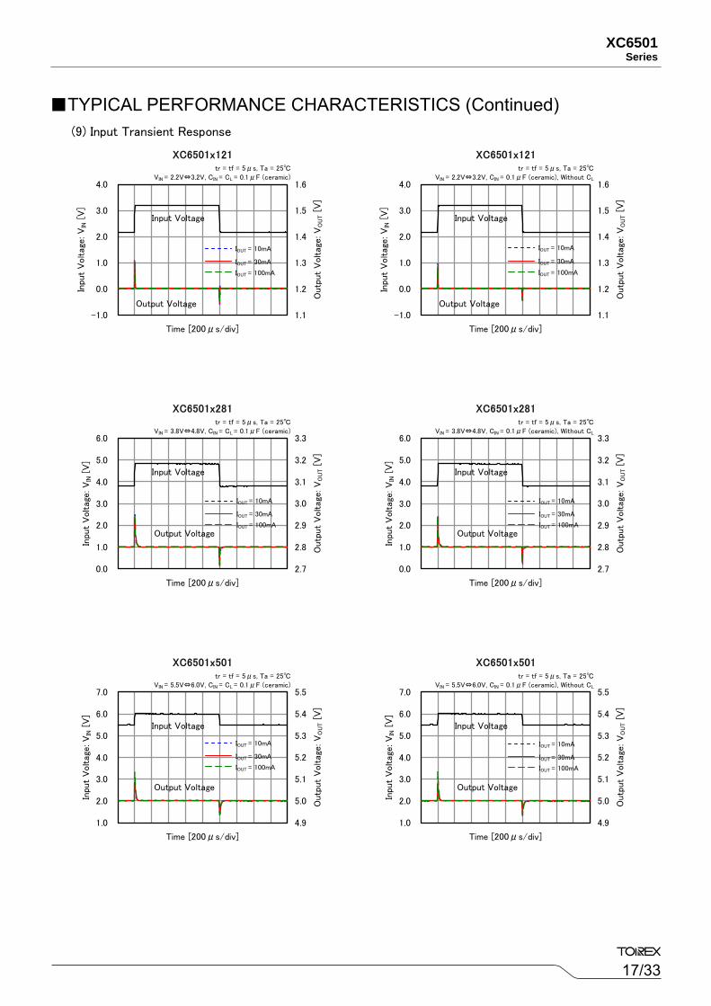
(9) Input Transient Response
tr = tf = 5μs, Ta = 25
VIN = 2.2V⇔3.2V, CIN = CL = 0.1μF (ceramic)
tr = tf = 5μs, Ta = 25VIN = 3.8V⇔4.8V, CIN = CL = 0.1μF (ceramic)
tr = tf = 5μs, Ta = 25VIN = 5.5V⇔6.0V, CIN = CL = 0.1μF (ceramic)
tr = tf = 5μs, Ta = 25VIN = 5.5V⇔6.0V, CIN = 0.1μF (ceramic), Without CL
tr = tf = 5μs, Ta = 25
VIN = 2.2V⇔3.2V, CIN = 0.1μF (ceramic), Without CL
tr = tf = 5μs, Ta = 25VIN = 3.8V⇔4.8V, CIN = 0.1μF (ceramic), Without CL
XC6501x121
-1.0
0.0
1.0
2.0
3.0
4.0
Time [200μs/div]
Inpu
t V
oltag
e: V
IN [
V]
1.1
1.2
1.3
1.4
1.5
1.6
Outp
ut
Voltag
e: V
OU
T [
V]
Input Voltage
Output Voltage
XC6501x121
-1.0
0.0
1.0
2.0
3.0
4.0
Time [200μs/div]
Inpu
t V
oltag
e: V
IN [
V]
1.1
1.2
1.3
1.4
1.5
1.6
Outp
ut
Voltag
e: V
OU
T [
V]
Input Voltage
Output Voltage
XC6501x281
0.0
1.0
2.0
3.0
4.0
5.0
6.0
Time [200μs/div]
Inpu
t V
oltag
e: V
IN [
V]
2.7
2.8
2.9
3.0
3.1
3.2
3.3
Outp
ut
Voltag
e: V
OU
T [
V]
Input Voltage
Output Voltage
XC6501x501
1.0
2.0
3.0
4.0
5.0
6.0
7.0
Time [200μs/div]
Inpu
t V
oltag
e: V
IN [
V]
4.9
5.0
5.1
5.2
5.3
5.4
5.5
Outp
ut
Voltag
e: V
OU
T [
V]
Input Voltage
Output Voltage
IOUT = 10mA
IOUT = 30mA
IOUT = 100mA
IOUT = 10mA
IOUT = 30mA
IOUT = 100mA
IOUT = 10mA
IOUT = 30mA
IOUT = 100mA
IOUT = 10mA
IOUT = 30mA
IOUT = 100mA
IOUT = 10mA
IOUT = 30mA
IOUT = 100mA
IOUT = 10mA
IOUT = 30mA
IOUT = 100mA
TYPICAL PERFORMANCE CHARACTERISTICS (Continued)
18/33
XC6501 Series
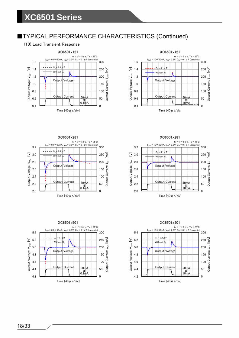
(10) Load Transient Response
tr = tf = 5μs, Ta = 25
IOUT = 0.1⇔50mA, VIN = 2.2V, CIN = 0.1μF (ceramic)
tr = tf = 5μs, Ta = 25
IOUT = 10⇔50mA, VIN = 2.2V, CIN = 0.1μF (ceramic)
tr = tf = 5μs, Ta = 25IOUT = 10⇔50mA, VIN = 3.8V, CIN = 0.1μF (ceramic)
tr = tf = 5μs, Ta = 25IOUT = 10⇔50mA, VIN = 6.0V, CIN = 0.1μF (ceramic)
tr = tf = 5μs, Ta = 25IOUT = 0.1⇔50mA, VIN = 6.0V, CIN = 0.1μF (ceramic)
tr = tf = 5μs, Ta = 25IOUT = 0.1⇔50mA, VIN = 3.8V, CIN = 0.1μF (ceramic)
XC6501x121
0.4
0.6
0.8
1.0
1.2
1.4
1.6
Time [40μs/div]
Outp
ut
Voltag
e: V
OU
T [
V]
0
50
100
150
200
250
300
Outp
ut
Curr
ent: I O
UT [
mA
]
XC6501x501
4.2
4.4
4.6
4.8
5.0
5.2
5.4
Time [40μs/div]
Outp
ut
Voltag
e: V
OU
T [
V]
0
50
100
150
200
250
300
Outp
ut
Curr
ent: I O
UT [
mA
]
XC6501x501
4.2
4.4
4.6
4.8
5.0
5.2
5.4
Time [40μs/div]
Outp
ut
Voltag
e: V
OU
T [
V]
0
50
100
150
200
250
300
Outp
ut
Curr
ent: I O
UT [
mA
]
XC6501x281
2.0
2.2
2.4
2.6
2.8
3.0
3.2
Time [40μs/div]
Outp
ut
Voltag
e: V
OU
T [
V]
0
50
100
150
200
250
300
Outp
ut
Curr
ent: I O
UT [
mA
]
XC6501x281
2.0
2.2
2.4
2.6
2.8
3.0
3.2
Time [40μs/div]
Outp
ut
Voltag
e: V
OU
T [
V]
0
50
100
150
200
250
300
Outp
ut
Curr
ent: I O
UT [
mA
]
XC6501x121
0.4
0.6
0.8
1.0
1.2
1.4
1.6
Time [40μs/div]
Outp
ut
Voltag
e: V
OU
T [
V]
0
50
100
150
200
250
300
Outp
ut
Curr
ent: I O
UT [
mA
]
⇔
Output Voltage
50mA
0.1mA
Output Current
⇔
Output Voltage
50mA
10mA
Output Current
⇔
Output Voltage
50mA
10mA
Output Current⇔
Output Voltage
50mA
0.1mA
Output Current
⇔
Output Voltage
50mA
0.1mA
Output Current
⇔
Output Voltage
50mA
10mA
Output Current
CL = 0.1μF
Without CL
CL = 0.1μF
Without CL
CL = 0.1μF
Without CL
CL = 0.1μF
Without CL
CL = 0.1μF
Without CL
CL = 0.1μF
Without CL
TYPICAL PERFORMANCE CHARACTERISTICS (Continued)
19/33
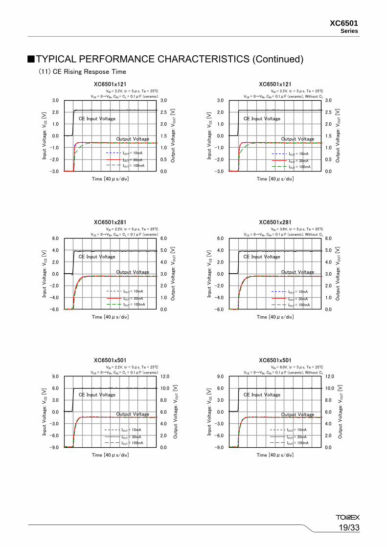
XC6501Series
(11) CE Rising Respose Time
VIN = 3.8V, tr = 5μs, Ta = 25
VCE = 0→VIN, CIN = 0.1μF (ceramic), Without CL
VIN = 6.0V, tr = 5μs, Ta = 25
VCE = 0→VIN, CIN = 0.1μF (ceramic), Without CL
VIN = 2.2V, tr = 5μs, Ta = 25
VCE = 0→VIN, CIN = CL = 0.1μF (ceramic)
VIN = 2.2V, tr = 5μs, Ta = 25
VCE = 0→VIN, CIN = CL = 0.1μF (ceramic)
VIN = 2.2V, tr = 5μs, Ta = 25
VCE = 0→VIN, CIN = 0.1μF (ceramic), Without CL
VIN = 2.2V, tr = 5μs, Ta = 25
VCE = 0→VIN, CIN = CL = 0.1μF (ceramic)
XC6501x121
-3.0
-2.0
-1.0
0.0
1.0
2.0
3.0
Time [40μs/div]
Inpu
t V
oltag
e: V
CE [
V]
0.0
0.5
1.0
1.5
2.0
2.5
3.0
Outp
ut
Voltag
e: V
OU
T [
V]
CE Input Voltage
Output Voltage
XC6501x121
-3.0
-2.0
-1.0
0.0
1.0
2.0
3.0
Time [40μs/div]
Inpu
t V
oltag
e: V
CE [
V]
0.0
0.5
1.0
1.5
2.0
2.5
3.0
Outp
ut
Voltag
e: V
OU
T [
V]
CE Input Voltage
Output Voltage
XC6501x281
-6.0
-4.0
-2.0
0.0
2.0
4.0
6.0
Time [40μs/div]
Inpu
t V
oltag
e: V
CE [
V]
0.0
1.0
2.0
3.0
4.0
5.0
6.0
Outp
ut
Voltag
e: V
OU
T [
V]
CE Input Voltage
Output Voltage
XC6501x501
-9.0
-6.0
-3.0
0.0
3.0
6.0
9.0
Time [40μs/div]
Inpu
t V
oltag
e: V
CE [
V]
0.0
2.0
4.0
6.0
8.0
10.0
12.0
Outp
ut
Voltag
e: V
OU
T [
V]
CE Input Voltage
Output Voltage
IOUT = 10mA
IOUT = 30mA
IOUT = 100mA
IOUT = 10mA
IOUT = 30mA
IOUT = 100mA
IOUT = 10mA
IOUT = 30mA
IOUT = 100mA
IOUT = 10mA
IOUT = 30mA
IOUT = 100mA
IOUT = 10mA
IOUT = 30mA
IOUT = 100mA
IOUT = 10mA
IOUT = 30mA
IOUT = 100mA
TYPICAL PERFORMANCE CHARACTERISTICS (Continued)
20/33
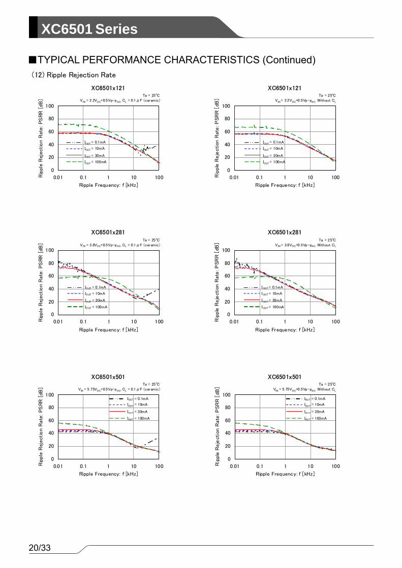
XC6501 Series
TYPICAL PERFORMANCE CHARACTERISTICS (Continued) (12) Ripple Rejection Rate
Ta = 25VIN = 2.2VDC+0.5Vp-pAC, Without CL
Ta = 25VIN = 2.2VDC+0.5Vp-pAC, CL = 0.1μF (ceramic)
Ta = 25VIN = 3.8VDC+0.5Vp-pAC, CL = 0.1μF (ceramic)
Ta = 25VIN = 5.75VDC+0.5Vp-pAC, CL = 0.1μF (ceramic)
Ta = 25VIN = 3.8VDC+0.5Vp-pAC, Without CL
Ta = 25VIN = 5.75VDC+0.5Vp-pAC, Without CL
XC6501x281
0
20
40
60
80
100
0.01 0.1 1 10 100
Ripple Frequency: f [kHz]
Rip
ple
Reje
ctio
n R
ate
: PSR
R [
dB]
XC6501x501
0
20
40
60
80
100
0.01 0.1 1 10 100
Ripple Frequency: f [kHz]
Rip
ple
Reje
ctio
n R
ate
: PSR
R [
dB]
XC6501x501
0
20
40
60
80
100
0.01 0.1 1 10 100
Ripple Frequency: f [kHz]
Rip
ple
Reje
ctio
n R
ate
: PS
RR
[dB
]
XC6501x281
0
20
40
60
80
100
0.01 0.1 1 10 100
Ripple Frequency: f [kHz]
Rip
ple
Reje
ctio
n R
ate
: PS
RR
[dB
]
XC6501x121
0
20
40
60
80
100
0.01 0.1 1 10 100
Ripple Frequency: f [kHz]
Rip
ple
Reje
ctio
n R
ate
: PS
RR
[dB
]
XC6501x121
0
20
40
60
80
100
0.01 0.1 1 10 100
Ripple Frequency: f [kHz]
Rip
ple R
eje
ctio
n R
ate
: PSR
R [
dB]
IOUT = 10mA
IOUT = 30mA
IOUT = 100mA
IOUT = 0.1mA
IOUT = 10mA
IOUT = 30mA
IOUT = 100mA
IOUT = 0.1mA
IOUT = 10mA
IOUT = 30mA
IOUT = 100mA
IOUT = 0.1mA
IOUT = 10mA
IOUT = 30mA
IOUT = 100mA
IOUT = 0.1mA
IOUT = 10mA
IOUT = 30mA
IOUT = 100mA
IOUT = 0.1mA
IOUT = 10mA
IOUT = 30mA
IOUT = 100mA
IOUT = 0.1mA
21/33
XC6501Series
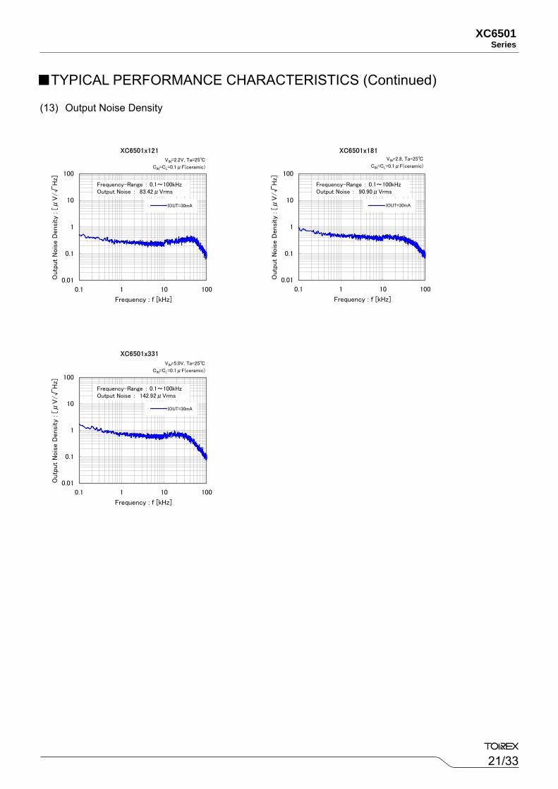
(13) Output Noise Density
TYPICAL PERFORMANCE CHARACTERISTICS (Continued)
XC6501x121
0.01
0.1
1
10
100
0.1 1 10 100
Frequency : f [kHz]
Outp
ut
Nois
e D
ensi
ty : [
μV
/√
Hz]
IOUT=30mA
VIN=2.2V, Ta=25
CIN=CL=0.1μF(ceramic)
Frequency-Range : 0.1~100kHz Output Noise : 83.42μVrms
XC6501x181
0.01
0.1
1
10
100
0.1 1 10 100
Frequency : f [kHz]
Outp
ut
Nois
e D
ensi
ty : [
μV
/√
Hz]
IOUT=30mA
VIN=2.8, Ta=25
CIN=CL=0.1μF(ceramic)
Frequency-Range : 0.1~100kHz Output Noise : 90.90μVrms
XC6501x331
0.01
0.1
1
10
100
0.1 1 10 100
Frequency : f [kHz]
Outp
ut
Nois
e D
ensi
ty : [
μV
/√
Hz]
IOUT=30mA
VIN=5.0V, Ta=25
CIN=CL=0.1μF(ceramic)
Frequency-Range : 0.1~100kHz Output Noise : 142.92μVrms
22/33
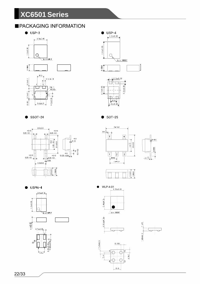
XC6501 Series
PACKAGING INFORMATION1.2±
0.08
0.6
MAX
0.2±
0.1
0.2±
0.05
(0.05
)0.7±
0.1
1.6±
0.08
MAX0
.6
0.7±
0.1
0.2
±0.1
1.6
+0.2
-0.1
2.8±
0.2
1.1±
0.1
1.3
MA
X
0.2M
IN
2.1±
0.3
0.9
±0.
11.2
5+0.2
-0.1
0.3
+0
-0.2
1.1M
AX
1.2±0.0
50.
38+0.0
2-0.0
3
0.2
5±
0.05
0.425
±0.05
2.0±0.1
2.1
±0.3
0.9±
0.1
0.125+0.1-0.05
1.3±0.2
0.25+0.15-0.1
1.2
5+0.
2-0.
1 0+0.1-0
0.3
+0
-0.
2
1.1M
AX
0.35+0.15-0.1
0.05
0.25+0.15-0.1
0.25+0.15-0.1
WLP-4-01
4 3
21
0.70±0.03
(0.150)
(0.4)
1pin INDENT
23/33
XC6501Series
PACKAGING INFORMATION (Continued)USP-3 Reference Pattern Layout USP-3 Reference Metal Mask Design
USP-4 Reference Pattern Layout USP-4 Reference Metal Mask Design
4 3
1 2 1 2
4 3
0.6
0.35 0.35
1.0 0.8
0.35 0.35
0.3
0.6
1.35
0.25
0.4
0.7
0.3
0.25
1.2
0.5
0.6
0.25
0.45
0.4
USPN-4 Reference Pattern Layout USPN-4 Reference Metal Mask Design
24/33
XC6501 Series 0.75
0.5
1.85
1.3
0.6
2.4
1.0
0.7
0.95 0.95
0.4
4-0.15
0.4
resist
0.15
0.27
PCB
4-0.15
0.4
0.4
PACKAGING INFORMATION (Continued)
SSOT-24 Reference Pattern Layout SOT-25 Reference Pattern Layout
WLP-4-01
Reference Pattern Layout
WLP-4-01
Reference Pattern Layout detail
WLP-4-01
Reference Metal Mask Design
25/33
XC6501Series
USPN-4 Power Dissipation
Power dissipation data for the USPN-4 is shown in this page.The value of power dissipation varies with the mount board conditions.Please use this data as the reference data taken in the following condition.
1. Measurement Condition
Condition: Mount on a boardAmbient: Natural convection
Soldering: Lead (Pb) freeBoard: Dimensions 40 x 40 mm
(1600 mm2 in one side)
Copper (Cu) traces occupy 50% of the front
and 50% of the back.
The copper area is divided into four block,
one block is 12.5% of total.
The USPN-4 package has for terminals.
Each terminal connects one copper block in
the front and one in the back.Material: Glass Epoxy (FR-4)
Thickness: 1.6 mmThrough-hole: 4 x 0.8 Diameter 評価基板レイアウト(単位:mm)
2.Power Dissipation vs. Ambient Temperature
Board Mount (Tj max = 125)Ambient Temperature() Power Dissipation Pd(mW) Thermal Resistance (/W)
25 600166.67
85 240
0
100
200
300
400
500
600
700
25 45 65 85 105 125
許容
損失
Pd(
mW
)
周囲温度Ta()
Pd-Ta特性グラフ
26/33
XC6501 Series
USP-4 Power Dissipation
Power dissipation data for the USP-4 is shown in this page.The value of power dissipation varies with the mount board conditions.Please use this data as the reference data taken in the following condition.
1. Measurement Condition
Condition: Mount on a boardAmbient: Natural convection
Soldering: Lead (Pb) freeBoard: Dimensions 40 x 40 mm
(1600 mm2 in one side) Copper (Cu) traces occupy 50% of the board area In top and back facesPackage heat-sink is tied to the copper traces
Material: Glass Epoxy (FR-4) Thickness: 1.6mm
Through-hole: 4 x 0.8 Diameter
2.Power Dissipation vs. Ambient Temperature Evaluation Board (Unit:mm)
Board Mount (Tj max = 125)Ambient Temperature() Power Dissipation Pd(mW) Thermal Resistance (/W)
25 1000100.00
85 400
0
200
400
600
800
1000
1200
25 45 65 85 105 125
Pow
er D
issi
patio
n P
d (m
W)
Ambient Temperature Ta ()
Pd vs Ta
40.0
28.9
2.54 1.4
27/33
XC6501Series
SSOT-24 Power Dissipation
Power dissipation data for the SSOT-24 is shown in this page.The value of power dissipation varies with the mount board conditions.Please use this data as the reference data taken in the following condition.
1. Measurement Condition
Condition: Mount on a boardAmbient: Natural convection
Soldering: Lead (Pb) freeBoard: Dimensions 40 x 40 mm
(1600 mm2 in one side) Copper (Cu) traces occupy 50% of the board area In top and back facesPackage heat-sink is tied to the copper traces
Material: Glass Epoxy (FR-4) Thickness: 1.6mm
Through-hole: 4 x 0.8 Diameter
Evaluation Board (Unit:mm)2.Power Dissipation vs. Ambient Temperature
Board Mount (Tj max = 125)Ambient Temperature() Power Dissipation Pd(mW) Thermal Resistance (/W)
25 500200.0085 200
0
100
200
300
400
500
600
25 45 65 85 105 125
Pow
er D
issi
patio
n P
d (m
W)
Ambient Temperature Ta ()
Pd vs Ta
28/33
XC6501 Series
SOT-25 Power Dissipation
Power dissipation data for the SOT-25 is shown in this page.The value of power dissipation varies with the mount board conditions.Please use this data as the reference data taken in the following condition.
1. Measurement Condition
Condition: Mount on a boardAmbient: Natural convection
Soldering: Lead (Pb) freeBoard: Dimensions 40 x 40 mm
(1600 mm2 in one side) Copper (Cu) traces occupy 50% of the boardarea In top and back facesPackage heat-sink is tied to the copper traces(Board of SOT-26 is used.)
Material: Glass Epoxy (FR-4) Thickness: 1.6mm
Through-hole: 4 x 0.8 Diameter
Evaluation Board (Unit:mm)2.Power Dissipation vs. Ambient Temperature
Board Mount (Tj max = 125)Ambient Temperature() Power Dissipation Pd(mW) Thermal Resistance (/W)
25 600166.67
85 240
0
100
200
300
400
500
600
700
25 45 65 85 105 125
Pow
er D
issi
patio
n P
d (m
W)
Ambient Temperature Ta ()
Pd vs. Ta
40.0
2.54 1.4
28.9
29/33
XC6501Series
USP-3 Power Dissipation
Power dissipation data for the USP-3 is shown in this page.The value of power dissipation varies with the mount board conditions.Please use this data as the reference data taken in the following condition.
1. Measurement Condition
Condition: Mount on a boardAmbient: Natural convection
Soldering: Lead (Pb) freeBoard: Dimensions 40 x 40 mm
(1600 mm2 in one side) Copper (Cu) traces occupy 50% of the board area In top and back facesPackage heat-sink is tied to the copper traces
Material: Glass Epoxy (FR-4) Thickness: 1.6mm
Through-hole: 4 x 0.8 Diameter
Evaluation Board (Unit:mm)2.Power Dissipation vs. Ambient Temperature
Board Mount (Tj max = 125)Ambient Temperature() Power Dissipation Pd(mW) Thermal Resistance (/W)
25 1000100.00
85 400
40.0
40.0
28.9
28.9
2.54 1.4
0
200
400
600
800
1000
1200
25 45 65 85 105 125
Pow
er D
issi
patio
n P
d (m
W)
Ambient Temperature Ta ()
Pd vs Ta
30/33
XC6501 Series
WLP-4-01 Power Dissipation
Power dissipation data for the WLP-4-01 is shown in this page.The value of power dissipation varies with the mount board conditions. Please use this data as the reference data taken in the following condition.
1. Measurement Condition
Condition : Mount on a boardAmbient : Natural convection
Soldering : Lead (Pb) freeBoard Dimensions : 40 x 40 mm (1600mm2)
Board Structure : 1st Meter layer about 50% 2nd Inner Metal layer about 50% 3rd Inner Metal layer about 50% 4th Metal layer about 50% 4 separations is each layer connected to each pin
Material : Glass Epoxy (FR-4)Thickness : 1.6 mm
Through-hole : 4 x 0.8 Diameter
Evaluation Board (Unit:mm)2. Power Dissipation vs. Ambient Temperature
Board Mount (Tj max = 125)Ambient Temperature()Power Dissipation Pd(mW)Thermal Resistance (/W)
25 660151.52
85 264
0
100
200
300
400
500
600
700
25 45 65 85 105 125
Pow
er D
issi
patio
n P
d (m
W)
Ambient Temperature Ta ()
Pd vs. Ta
2.54 1.4
40.0
40.0
2.5
28.9
28.9
31/33
XC6501Series
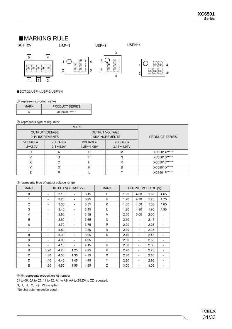
SOT-25/USP-4/USP-3/USPN-4 ① represents product series
MARK PRODUCT SERIES
A XC6501****** ② represents type of regulator
MARK
PRODUCT SERIES OUTPUT VOLTAGE 0.1V INCREMENTS
OUTPUT VOLTAGE 0.05V INCREMENTS
VOLTAGE= 1.2~3.0V
VOLTAGE= 3.1~5.0V
VOLTAGE= 1.25~3.05V
VOLTAGE= 3.15~4.95V
U A E M XC6501A***** V B F N XC6501B***** X C H R XC6501C***** Y D K S XC6501D***** Z P L T XC6501P*****
③ represents type of output voltage range
MARK OUTPUT VOLTAGE (V) MARK OUTPUT VOLTAGE (V)
0 - 3.10 - 3.15 F 1.60 4.60 1.65 4.65 1 - 3.20 - 3.25 H 1.70 4.70 1.75 4.75 2 - 3.30 - 3.35 K 1.80 4.80 1.85 4.85 3 - 3.40 - 3.45 L 1.90 4.90 1.95 4.95 4 - 3.50 - 3.55 M 2.00 5.00 2.05 - 5 - 3.60 - 3.65 N 2.10 - 2.15 - 6 - 3.70 - 3.75 P 2.20 - 2.25 - 7 - 3.80 - 3.85 R 2.30 - 2.35 - 8 - 3.90 - 3.95 S 2.40 - 2.45 - 9 - 4.00 - 4.05 T 2.50 - 2.55 - A - 4.10 - 4.15 U 2.60 - 2.65 - B 1.20 4.20 1.25 4.25 V 2.70 - 2.75 - C 1.30 4.30 1.35 4.35 X 2.80 - 2.85 - D 1.40 4.40 1.45 4.45 Y 2.90 - 2.95 - E 1.50 4.50 1.55 4.55 Z 3.00 - 3.05 -
④,⑤ represents production lot number 01 to 09, 0A to 0Z, 11 to 9Z, A1 to A9, AA to Z9,ZA to ZZ repeated. G,I,J,O,Q,W excepted. *No character inversion used.
1 2 3
5 4
① ② ③ ④ ⑤
SOT-25
③
1
2
4
3
①②④
⑤
USP-4 USP-3
1
2
3
3
③①
②④⑤
USPN-4
1
2
4
3
① ②
④ ⑤③
MARKING RULE
32/33
XC6501 Series
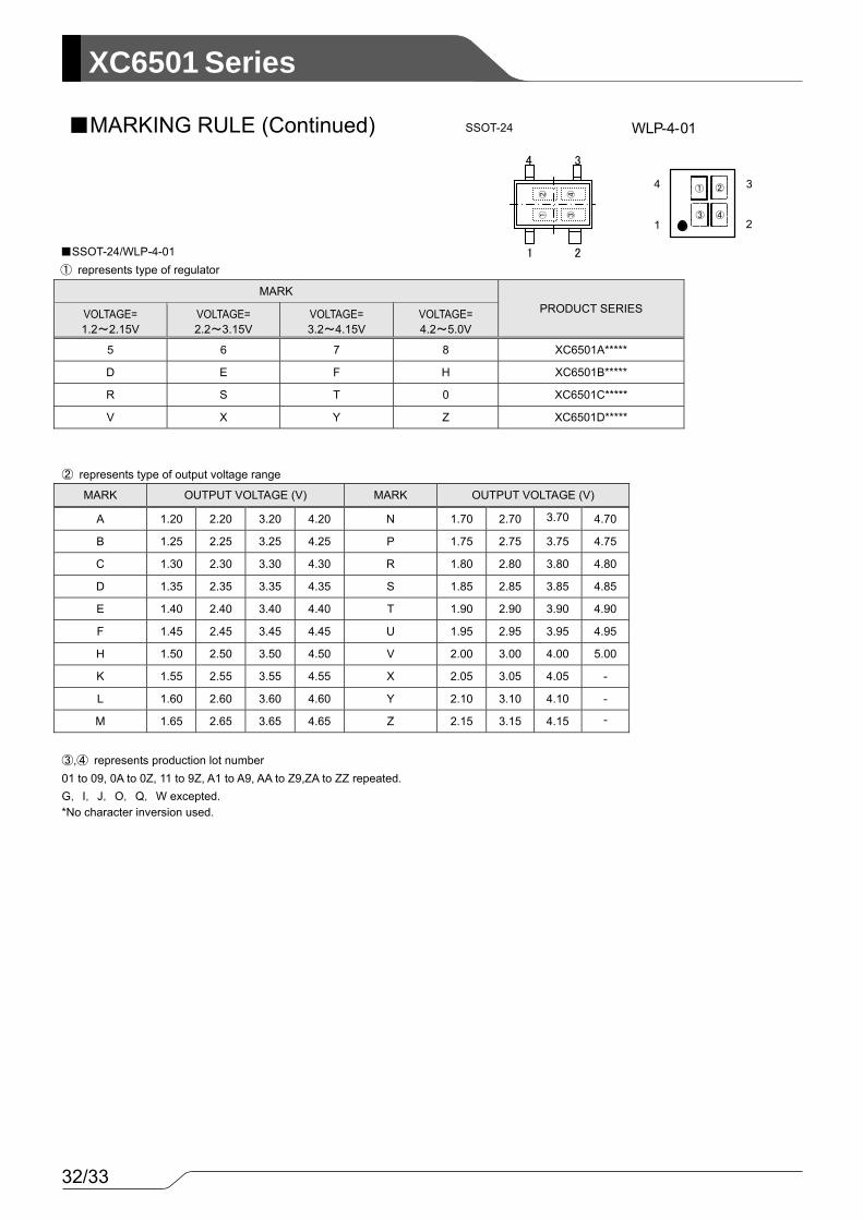
MARK PRODUCT SERIES VOLTAGE=
1.2~2.15V VOLTAGE= 2.2~3.15V
VOLTAGE= 3.2~4.15V
VOLTAGE= 4.2~5.0V
5 6 7 8 XC6501A*****
D E F H XC6501B*****
R S T 0 XC6501C*****
V X Y Z XC6501D*****
② represents type of output voltage range
MARK OUTPUT VOLTAGE (V) MARK OUTPUT VOLTAGE (V)
A 1.20 2.20 3.20 4.20 N 1.70 2.70 3.70 4.70
B 1.25 2.25 3.25 4.25 P 1.75 2.75 3.75 4.75
C 1.30 2.30 3.30 4.30 R 1.80 2.80 3.80 4.80
D 1.35 2.35 3.35 4.35 S 1.85 2.85 3.85 4.85
E 1.40 2.40 3.40 4.40 T 1.90 2.90 3.90 4.90
F 1.45 2.45 3.45 4.45 U 1.95 2.95 3.95 4.95
H 1.50 2.50 3.50 4.50 V 2.00 3.00 4.00 5.00
K 1.55 2.55 3.55 4.55 X 2.05 3.05 4.05 -
L 1.60 2.60 3.60 4.60 Y 2.10 3.10 4.10 -
M 1.65 2.65 3.65 4.65 Z 2.15 3.15 4.15 -
③,④ represents production lot number 01 to 09, 0A to 0Z, 11 to 9Z, A1 to A9, AA to Z9,ZA to ZZ repeated. G,I,J,O,Q,W excepted. *No character inversion used.
SSOT24
④
1 2
34
③
②①
SSOT-24
SSOT-24/WLP-4-01 ① represents type of regulator
MARKING RULE (Continued) WLP-4-01
① ②
④③1 2
34
33/33
XC6501Series
1. The product and product specifications contained herein are subject to change without notice to
improve performance characteristics. Consult us, or our representatives before use, to confirm that the information in this datasheet is up to date.
2. The information in this datasheet is intended to illustrate the operation and characteristics of our
products. We neither make warranties or representations with respect to the accuracy or completeness of the information contained in this datasheet nor grant any license to any intellectual property rights of ours or any third party concerning with the information in this datasheet.
3. Applicable export control laws and regulations should be complied and the procedures required by
such laws and regulations should also be followed, when the product or any information contained in this datasheet is exported.
4. The product is neither intended nor warranted for use in equipment of systems which require
extremely high levels of quality and/or reliability and/or a malfunction or failure which may cause loss of human life, bodily injury, serious property damage including but not limited to devices or equipment used in 1) nuclear facilities, 2) aerospace industry, 3) medical facilities, 4) automobile industry and other transportation industry and 5) safety devices and safety equipment to control combustions and explosions. Do not use the product for the above use unless agreed by us in writing in advance.
5. Although we make continuous efforts to improve the quality and reliability of our products;
nevertheless Semiconductors are likely to fail with a certain probability. So in order to prevent personal injury and/or property damage resulting from such failure, customers are required to incorporate adequate safety measures in their designs, such as system fail safes, redundancy and fire prevention features.
6. Our products are not designed to be Radiation-resistant.
7. Please use the product listed in this datasheet within the specified ranges.
8. We assume no responsibility for damage or loss due to abnormal use.
9. All rights reserved. No part of this datasheet may be copied or reproduced unless agreed by Torex
Semiconductor Ltd in writing in advance.
TOREX SEMICONDUCTOR LTD.


![DV 0LH 3RWHQ]LDO XQG GDV /HQQDUG -RQHV 3RWHQ]LDO · 2020. 8. 17. · 'dv 0lh 3rwhq]ldo xqg gdv /hqqdug -rqhv 3rwhq]ldo 0lw 3rwhq]ldo 0rghoohq ehvfkuhlew pdq glh (qhujlh ]zlvfkhq](https://img.pdfslide.net/doc/110x75/604fd29954d5e9155f201bd8/dv-0lh-3rwhqldo-xqg-gdv-hqqdug-rqhv-3rwhq-2020-8-17-dv-0lh-3rwhqldo.jpg)