Embed Size (px)
Citation preview
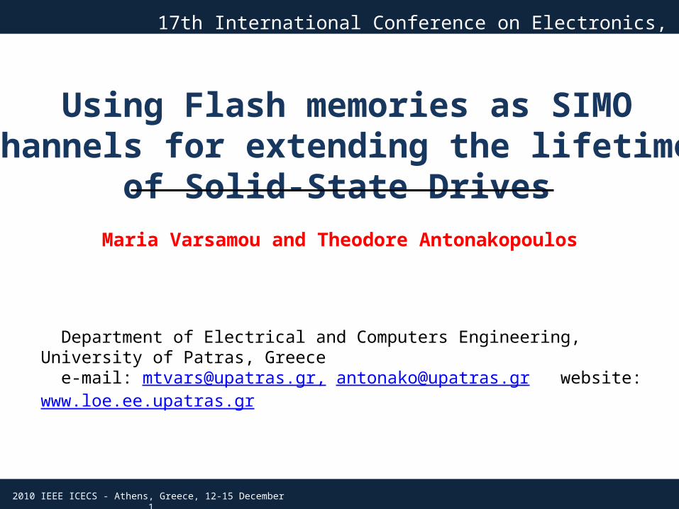
2010 IEEE ICECS - Athens, Greece, 12-15 December 1
Using Flash memories as SIMO channels for extending the lifetime of Solid-State Drives
Maria Varsamou and Theodore Antonakopoulos
Department of Electrical and Computers Engineering, University of Patras, Greece e-mail: [email protected], [email protected] website: www.loe.ee.upatras.gr
17th International Conference on Electronics, Circuits, and Systems
2010 IEEE ICECS - Athens, Greece, 12-15 December 2
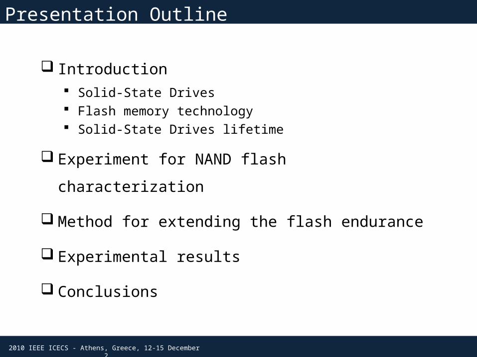
Presentation Outline
Introduction Solid-State Drives Flash memory technology Solid-State Drives lifetime
Experiment for NAND flash characterization
Method for extending the flash endurance
Experimental results
Conclusions

2010 IEEE ICECS - Athens, Greece, 12-15 December 3
Solid-State Drives (SSDs)
SSDs have become a mature solution for consumer and enterprise applications
SSDs have to demonstrate similar or better performance compared to magnetic disks
SSDs performance metrics: Data reliability (retention and endurance) I/O performance (kIOPs and latency)
SSDs use Flash memories (SLC/MLC) SSDs performance depends on:
Used Flash technology Supported workload Internal architecture High-level functions
Flash memory demonstrates a time-varying behavior in terms of raw BER and wears out as workload (P/E cycles) increases
DRAMmemory
Flash Channel #1FCC
FlashDie
FlashDie
Flash Channel #MFCC
FlashDie
FlashDie
MainProcessor
DRAMmemory
HostInterface
DMAengines
2010 IEEE ICECS - Athens, Greece, 12-15 December 4
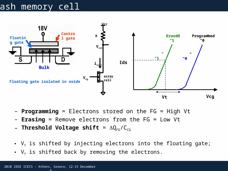
• VT is shifted by injecting electrons into the floating gate;
• VT is shifted back by removing the electrons.
Control gateFloating
gate
Bulk
Flash memory cell
Vcc
R
icell
array cell
Vcell
Vcg
Ids
Vcg
“1” “0”
Erased“1”
Programmed“0”
Vt
– Programming = Electrons stored on the FG = High Vt– Erasing = Remove electrons from the FG = Low Vt– Threshold Voltage shift = QFG/CCG
Floating gate isolated in oxide

2010 IEEE ICECS - Athens, Greece, 12-15 December 5
Retention: capability of keeping the stored information in time.
Endurance: capability of maintaining the stored information after erase, program and read cycling.
High voltages are applied during block erase (all pages of a block)page program (all cells of a page and adjacent pages)
And a high electric field is applied to the tunnel oxide and that results to oxide aging.
Flash memory error conditions
More frequent error conditions Variations on the stored charge (more permanent errors) Variations on the detected voltage during read (more temporary errors) Shift in operating margin (more permanent errors)
Probability 1 0 is much higher than the probability 0 1
1 0 typical error condition during the life-time of a flash cell0 1 error condition only at the end of the life-time of a flash cell

2010 IEEE ICECS - Athens, Greece, 12-15 December 6
Typical NAND IC Architecture
A number of NAND Flash cells forms a page A number of pages forms a block Read/Write per page Erase per block Overwriting is not permitted
NAND Interfaces ONFI 1.0 Asynchronous
40 Mbytes/sec ONFI 2.0 Synchronous
166/200 Mbytes/sec
2010 IEEE ICECS - Athens, Greece, 12-15 December 7
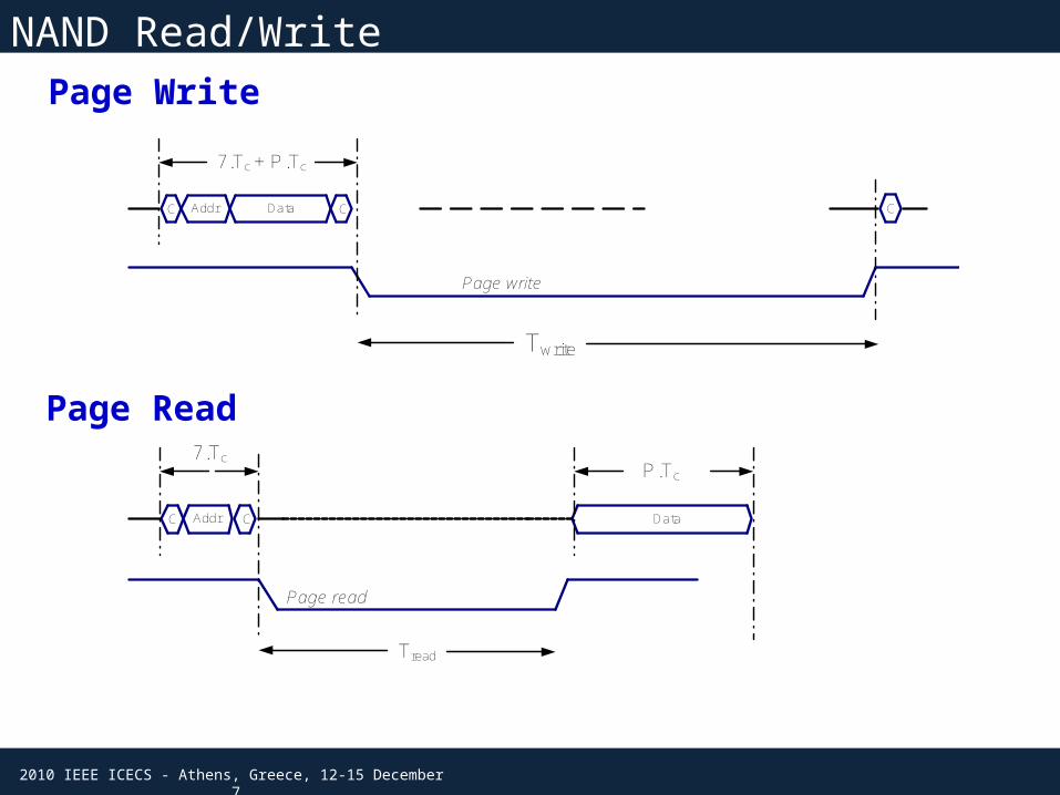
NAND Read/Write
7.Tc
Page read
CC Addr Data
Tread
P.Tc
7.Tc + P.Tc
Page write
CC Addr Data C
Twrite
Page Write
Page Read

2010 IEEE ICECS - Athens, Greece, 12-15 December 8
Type Std SLC MLC Enterprise MLC
Consumer MLC
Interface ONFI2.0 ONFI2.0 ONFI2.0 ONFI2.0
Capacity per NAND Die (Gbits) 16 16 32 32
Page size (bytes) 4K+224 4K+224 4K+224 4K+224
Pages per block 128 128 256 256
Page Read (usecs) 25 50 50 50
Page Write (usecs) 200 700 1600 900
Block Erase (usecs) 700 2000 4000 3000
max Sustained READ Data Rate (MBps)
80 53 53 53
max Sustained WRITE Data Rate (MBps)
18 5 2.5 4.4
Endurance (Pr/Er cycles) 100K 10K 30K 5K
NAND Flash memory
2010 IEEE ICECS - Athens, Greece, 12-15 December 9
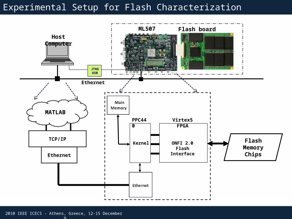
Experimental Setup for Flash Characterization
Ethernet
Host Computer
JTAGUSB
ML507 Flash board
PPC440 Virtex5 FPGA
Kernel ONFI 2.0 Flash Interface
Ethernet
TCP/IPFlash Memory
Chips
MATLAB

2010 IEEE ICECS - Athens, Greece, 12-15 December 10
Raw BER of SLC Flash memory
0 100 200 300 400 500 600 700 800 900 100010
-6
10-5
10-4
10-3
P/E Rounds [K]
Bit
Err
or
Ra
te
BlockBest Page
Worst Page
Bit E
rror
Rati
o (B
ER)

2010 IEEE ICECS - Athens, Greece, 12-15 December 11
50 100 150 200 250
10-6
10-5
10-4
10-3
10-2
10-1
P/E Rounds [K]
Bit
Err
or R
atio
(B
ER
)
Block
Worst Page
1st Page with Single Error
Best Page
Raw BER of MLC Flash memory

2010 IEEE ICECS - Athens, Greece, 12-15 December 12
Methods for extending the Lifetime of SSDs
Error Correction Codes (BCH, RS, LDPC etc., additional parity information)
Wear-leveling (System level, intra-block)
Exploit the characteristics of the error insertion mechanism (proposed method)
S ELifetime
V A
S : user space
E : endurance (number of P/E cycles)
V : user written space per time unit
A : write amplification

2010 IEEE ICECS - Athens, Greece, 12-15 December 13
SLC Endurance Measurements
0 200 400 600 800 1000
10-4
P/E cycles [K]
raw
BE
R
Page Size: 4320 bytes Experiment: Erase block, Write all pages with random data, Read all pages, Compare
Target user BER: 10-15
1
0
1
0
Tx Rx
SLC Channel Model

2010 IEEE ICECS - Athens, Greece, 12-15 December 14
Extending the endurance
nW
+ +Write
nR
+
+
Read #1
Read #N
nR
nR
BCH (n, k) code: error correction capability of t-error bits
BCH error correction capability can be extended to 2t using erasures
The errors can be:
Write and Read related Permanent and Temporary
The SLC channel inserts errors that only change the bits from ‘1’ to ‘0’
We read the corrupted page additional times and estimate erasures according to bit differences
SISO
SIMO

2010 IEEE ICECS - Athens, Greece, 12-15 December 15
Proposed Correction Method
Calculate BCH syndromes
Syndromes = 0? PAGE CORRECT
YES
NO
YES
NO
START
Read Page Store data in Buffer_1
Read Page one additional time
XOR new data with data in Buffer
BCH Decode
Error locations found?PAGE
CORRECT
PAGE WITH ERRORS
Iterations ≤ N? YES
NO
Keep data in Buffer
Buffer
Flash Channel
Dataa a
b
b
to ECC decoder
Hardware complexity
The correction mechanism is activated only when the user data can not be recovered. In this case, a small delay is introduced, comparable with the delay introduced during BCH decoding.
Data
Syndromes
Error locator/Correction
Data
Syndromes
Error locator/Correction
Data

2010 IEEE ICECS - Athens, Greece, 12-15 December 16
0 100 200 300 400 500 600 700 800 900 1000
10-4
P/E cycles [K]
raw
BE
R
1 Read cycle3 Read cycles5 Read cycles
+16%
+25%
Performance of the proposed method
As the number of read cycles increases, the method's performance also improves, but with less gain.

2010 IEEE ICECS - Athens, Greece, 12-15 December 17
Effect on Flash Controller I/O Performance
DRAMmemory
Flash Channel #1FCC
FlashDie
FlashDie
Flash Channel #MFCC
FlashDie
FlashDie
MainProcessor
DRAMmemory
HostInterface
DMAengines
Flash Controller Architecture Today’s high performance SSDs support:
Large number of Flash channels, usually 16 A few Gbytes of SLC memory are used per
channel Host interface data rate of a few Gbps
Expected I/O Rate for 16 channels: ~ 300 KIOPs, no pipeline ~ 600 KIOPs, with pipeline
Measured I/O Rate: ~ 120 KIOPs
Limited by: Internal architecture Latency introduced by ECC Flash related functions (wear leveling, garbage
collection, etc.)
The proposed method for extending flash endurance does not decrease the SSD’s storage efficiency (no additional parity) and does not affect the I/O performance as long as the used ECC can correct all errors.

2010 IEEE ICECS - Athens, Greece, 12-15 December 18
Conclusions
The lifetime of an SSD can be extended by improving the endurance of its Flash memories
A method that exploits the error characteristics of SLC Flash memory to identify possible error locations was proposed: Sustains the memory endurance for a few tens of thousands P/E cycles Limited hardware complexity No additional parity bits are required (No decrease the SSD’s storage
efficiency).
Does not affect the SSD’s I/O performance during normal operation and as long as the used ECC scheme can recover any corrupted data.