Embed Size (px)
Citation preview

This training will cover the 2010 Plasma, LCD and LED televisions showing the new features, changes in design and troubleshooting tips for the 2010 model year.
1

Comparison of the 2009 to the 2010 LED model TV’s show an increase in contrast ratio.
2

A new energy saving feature on the 2010 Samsung TV’s is the ECO Sensor which will adjust the brightness of the screen according to the lighting in the room. The viewer has the ability to turn this feature off if desired.
3
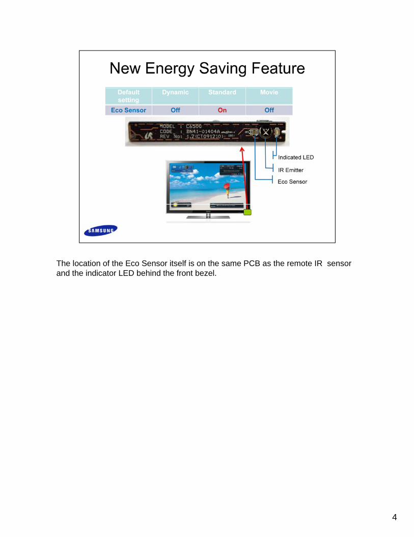
The location of the Eco Sensor itself is on the same PCB as the remote IR sensor and the indicator LED behind the front bezel.
4
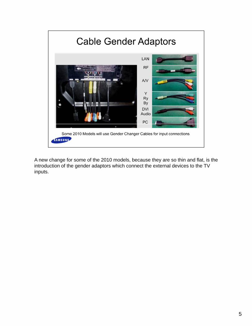
A new change for some of the 2010 models, because they are so thin and flat, is the introduction of the gender adaptors which connect the external devices to the TV inputs.
5

Firmware upgrades can be accomplished is different ways depending on the available features of the model of TV. The usual way is through a USB drive containing the upgrade file.
6

Over the Network (OTN) can inform the customer of available firmware versions. If the TV has the ability to connect to the internet through a home network, this is another method of upgrading the firmware. Additionally the customer can reload the stored older version of the software by selecting alternative software.
7
8

9
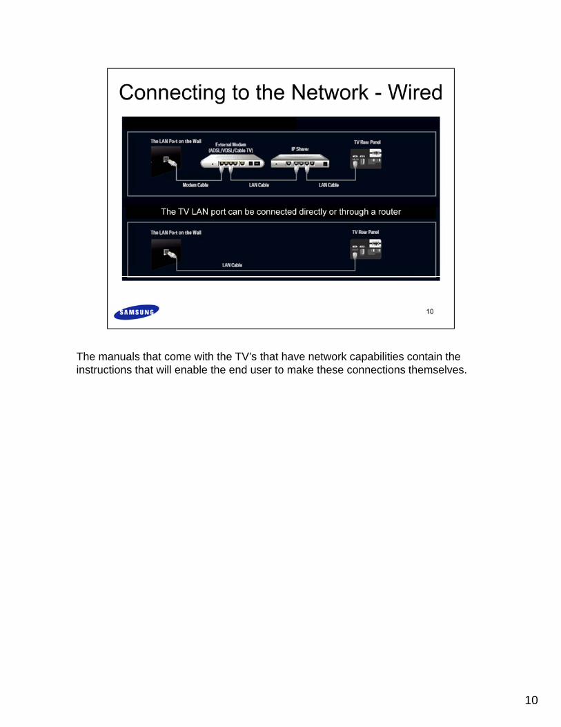
The manuals that come with the TV’s that have network capabilities contain the instructions that will enable the end user to make these connections themselves.
10

In a simple wired system, as in a computer, there is a automatic function that will find the address of the network by itself. Just select the “Auto Setup” function once the cable is connected.
11

To manually enter the proper address select manual setup and enter the address using the remote.
12
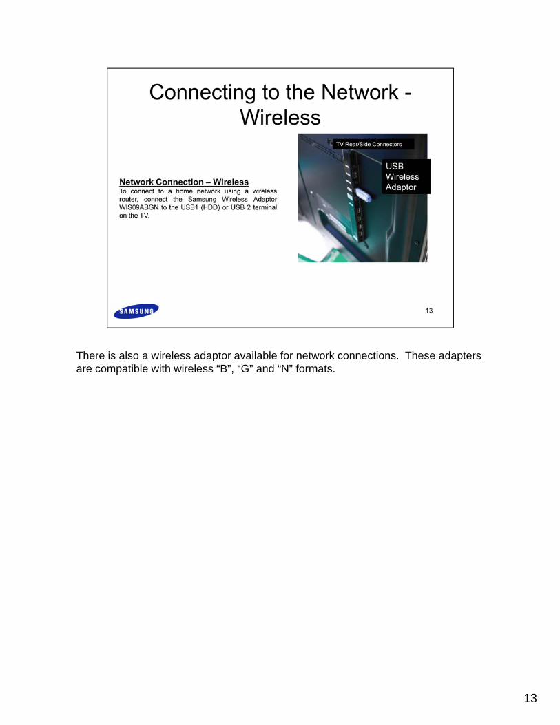
There is also a wireless adaptor available for network connections. These adapters are compatible with wireless “B”, “G” and “N” formats.
13

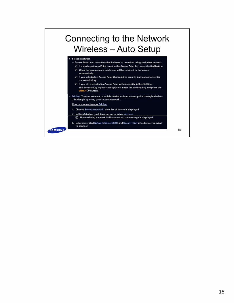
As in the wired setup, if the network is an open system use the auto setup function. The wireless option will only appear in the menu when the wireless adaptor is connected to the USB socket.
14
15
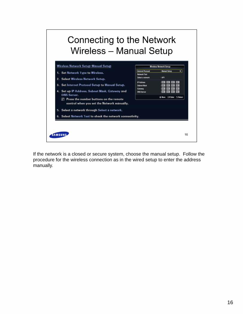
If the network is a closed or secure system, choose the manual setup. Follow the procedure for the wireless connection as in the wired setup to enter the address manually.
16

17

The LAN testing procedure is the same as in prior model years by creating a simple loop back device to plug into the LAN connector.
18
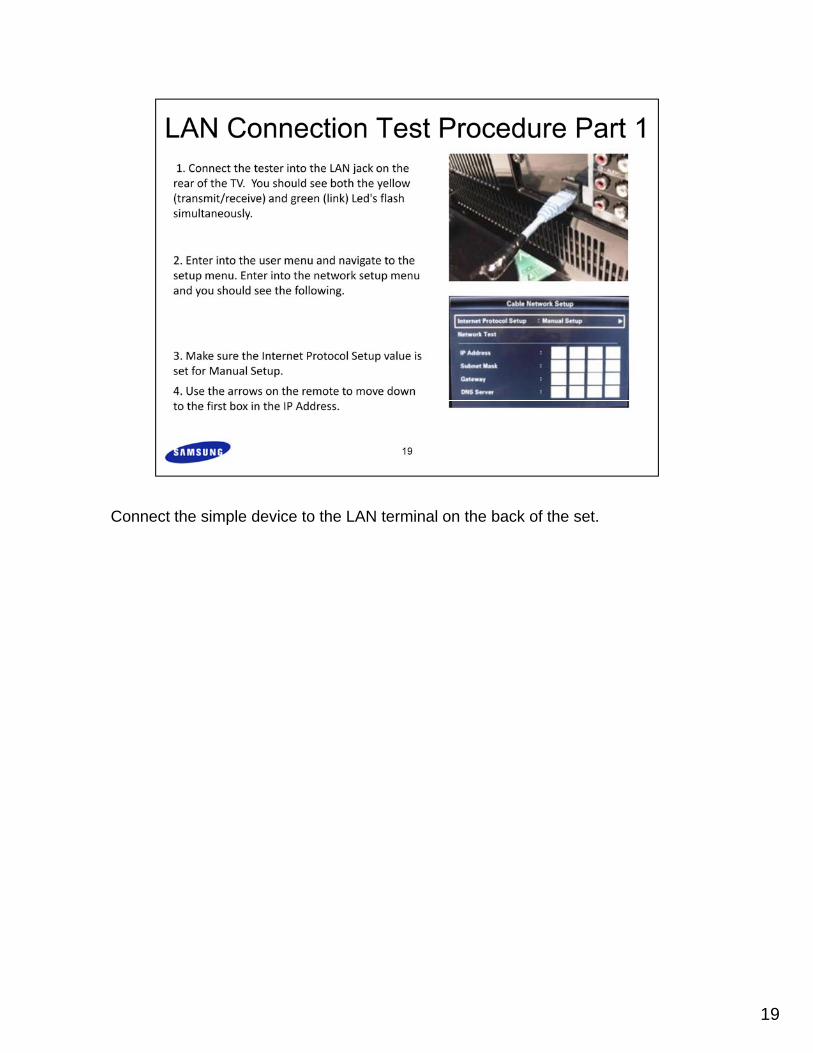
Connect the simple device to the LAN terminal on the back of the set.
19

Enter the address as shown and select the network test. MAC and IP must show a check mark if the internal circuits on the main PCB are working. If an X should appear by either one, replace the main PCB.
20

If the speed of the connection is too slow the video will look very poor or may freeze while viewing.
21

The speed of the connection is important as the applications will not run properly if the connection speed is too slow.1. In the menu go to “Setup” and select “Content View”2. 2. Select “Internet@TV”3. 3. Select “Settings”
22

4. Under settings select “Properties”5. Select “Check the speed of your internet connection”
23
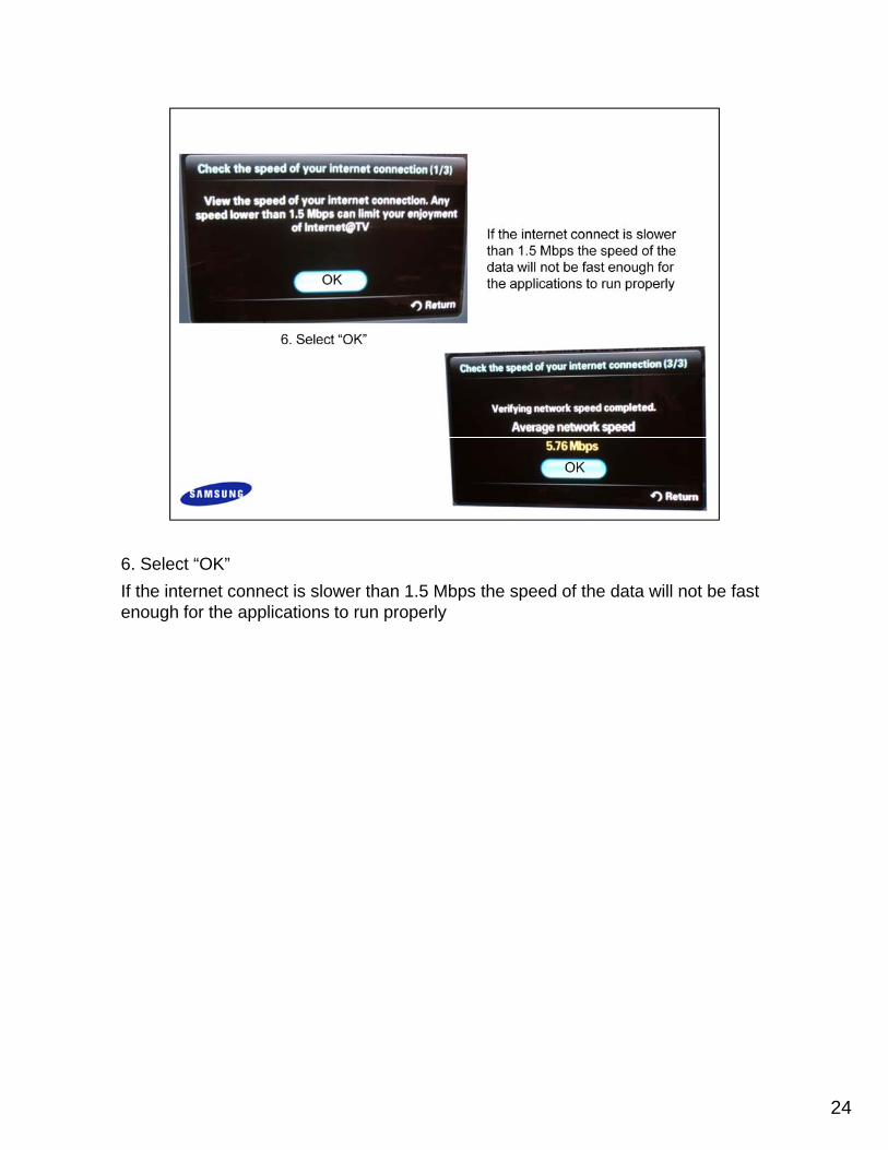
6. Select “OK”If the internet connect is slower than 1.5 Mbps the speed of the data will not be fast enough for the applications to run properly
24

25

Power supply removal requires the tech to remove either 6 or 8 screws be removed depending on the model and size of screen. After replacement of the SMPS make sure the voltages are adjusted according to the label posted on the panel.
26
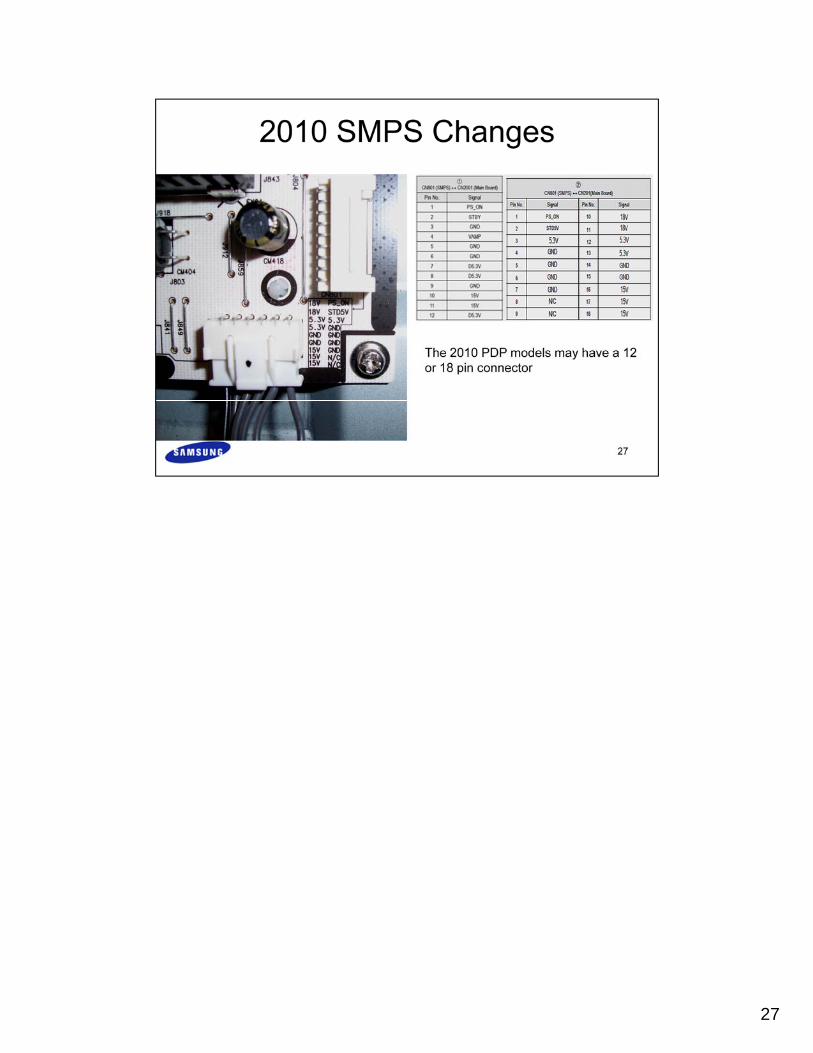
27
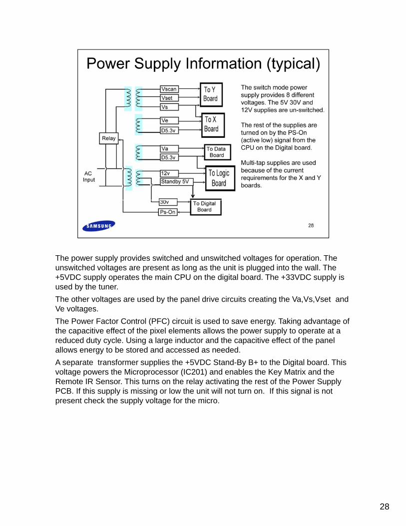
The power supply provides switched and unswitched voltages for operation. The unswitched voltages are present as long as the unit is plugged into the wall. The +5VDC supply operates the main CPU on the digital board. The +33VDC supply is used by the tuner. The other voltages are used by the panel drive circuits creating the Va,Vs,Vset and Ve voltages. The Power Factor Control (PFC) circuit is used to save energy. Taking advantage of the capacitive effect of the pixel elements allows the power supply to operate at a reduced duty cycle. Using a large inductor and the capacitive effect of the panel allows energy to be stored and accessed as needed.A separate transformer supplies the +5VDC Stand-By B+ to the Digital board. This voltage powers the Microprocessor (IC201) and enables the Key Matrix and the Remote IR Sensor. This turns on the relay activating the rest of the Power Supply PCB If thi l i i i l th it ill t t If thi i l i tPCB. If this supply is missing or low the unit will not turn on. If this signal is not present check the supply voltage for the micro.
28

If the Ve voltage is low or missing disconnect the power supply cable from the X board. If the Ve voltage rises the X board is probably shorted. If the voltage stays low the SMPS board needs to be replaced. If the Vs voltage is low or missing it can be caused by a defective X or Y board. Check both boards for short circuits before replacing the SMPS board. If the Vs voltage is too high an effect called diffusion may occur. Diffusion is when the initialize voltage is too high. Excessive voltage causes unwanted pixel firing creating intermittent sub-pixel flashes. Power on-off cycling can be caused by a shorted component on the Logic board loading down thecycling can be caused by a shorted component on the Logic board loading down the standby 5V.
29

If the Ve voltage is low or missing disconnect the power supply cable from the X board. If the Ve voltage rises the X board is probably shorted. If the voltage stays low the SMPS board needs to be replaced. If the Vs voltage is low or missing it can be caused by a defective X or Y board. Check both boards for short circuits before replacing the SMPS board. If the Vs voltage is too high an effect called diffusion may occur. Diffusion is when the initialize voltage is too high. Excessive voltage causes unwanted pixel firing creating intermittent sub-pixel flashes. Power on-off cycling can be caused by a shorted component on the Logic board loading down thecycling can be caused by a shorted component on the Logic board loading down the standby 5V.
30

Each plasma panel has a unique voltage setting required to display a picture properly and maintain long life. Incorrect adjustment of the power supply can create picture errors. Whenever a power supply board is replaced the new board must be adjusted to match the panel values shown on the sticker.If a power supply board is replaced it is imperative that the new power supply be adjusted to match the existing panel settings. Incorrect adjustment can cause the picture to be too dark or too bright. Extreme misadjustment can greatly reduce
l lifpanel life.
Locations of the test points and adjustments on a typical SMPS power supply. These adjustments must be performed when the SMPS or the panel is replacedThese adjustments must be performed when the SMPS or the panel is replaced.
31

Over Voltage Protection .The Power Supply PCB has an Over Voltage Protection circuit as well as a regulator circuit. It is designed so that when an Over Voltage condition occurs in any part of the power supply it does not affect another output stage. The following table shows the Over Voltage specifications. The unit must be unplugged to reset this error. Intermittent shutdown may be caused by an over-voltage condition.Over Current ProtectionFor this Power Supply PCB if a short circuit occurs on either the VS, VA, 12V, 6V or 3.3V lines, the SMPS stops operating, but should not fail. When the short circuit is removed from the source line the Power Supply will operate normally again.
32
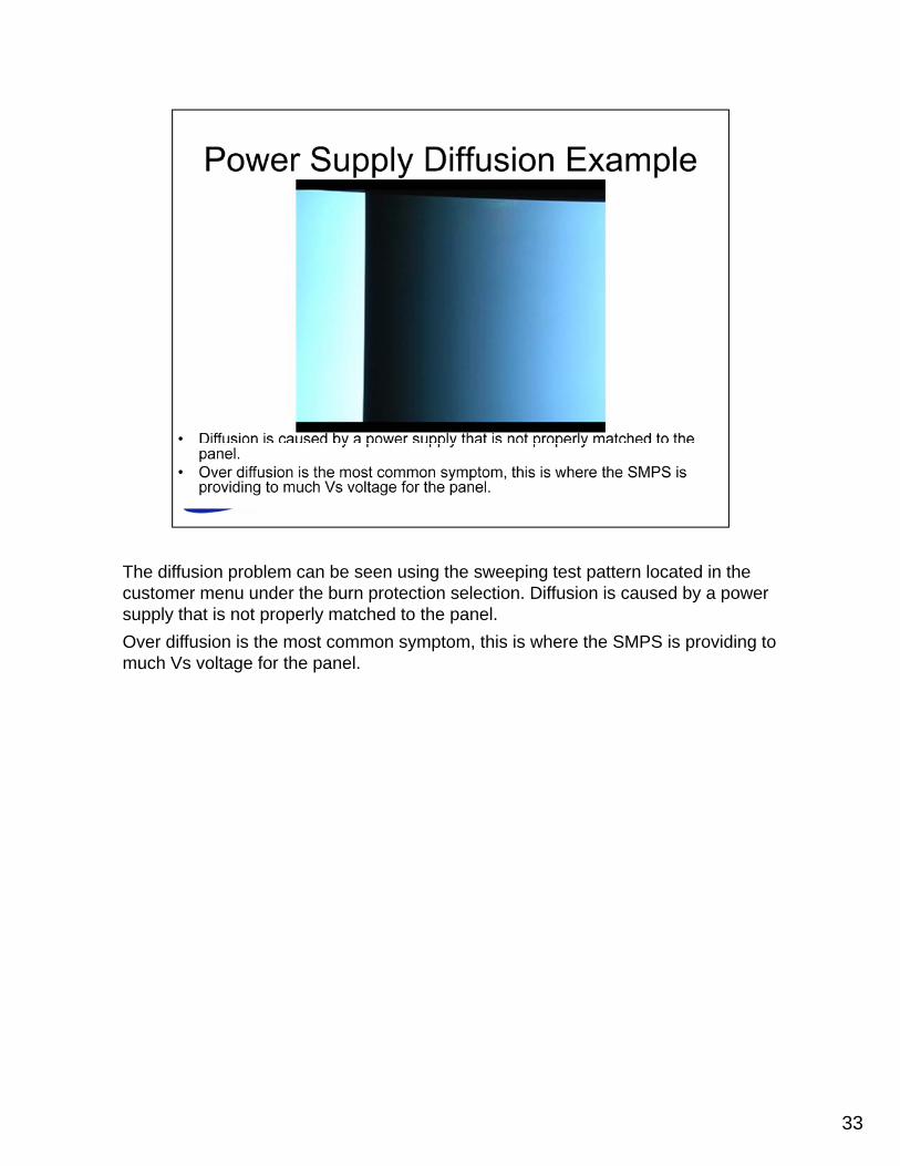
The diffusion problem can be seen using the sweeping test pattern located in the customer menu under the burn protection selection. Diffusion is caused by a power supply that is not properly matched to the panel.Over diffusion is the most common symptom, this is where the SMPS is providing to much Vs voltage for the panel.
33
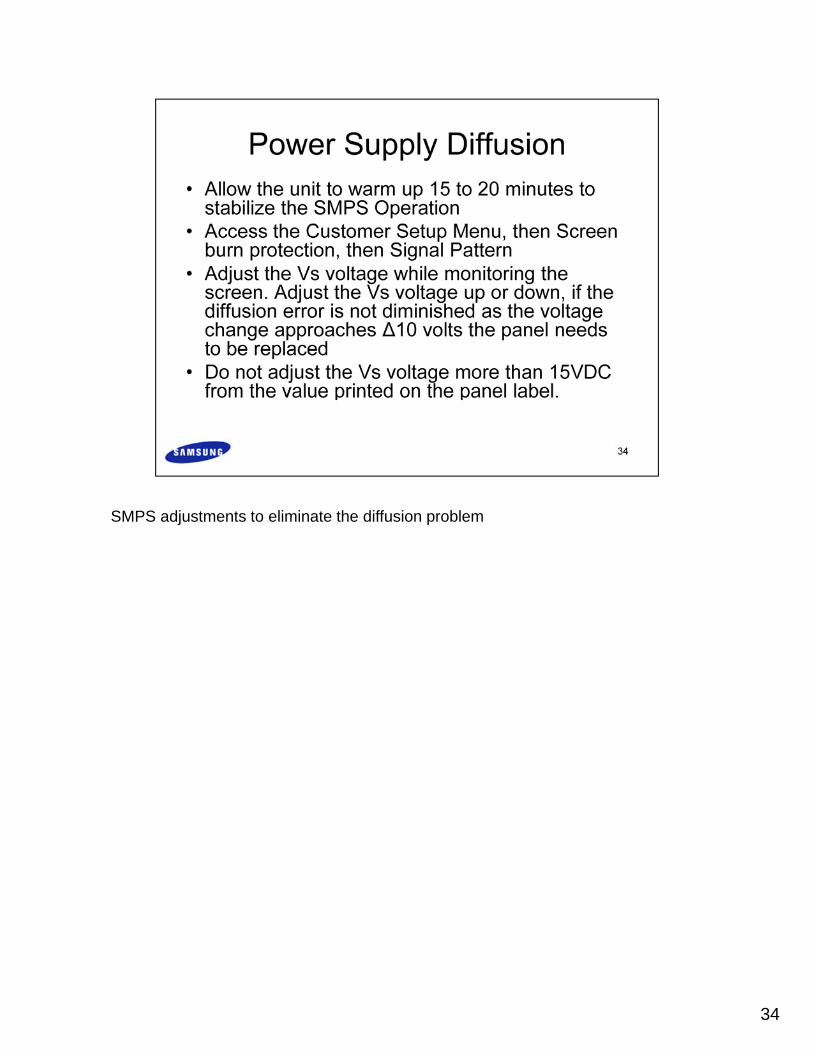
SMPS adjustments to eliminate the diffusion problem
34
35

The latest LED SMPS controls the PWM to the LED backlight array.
36
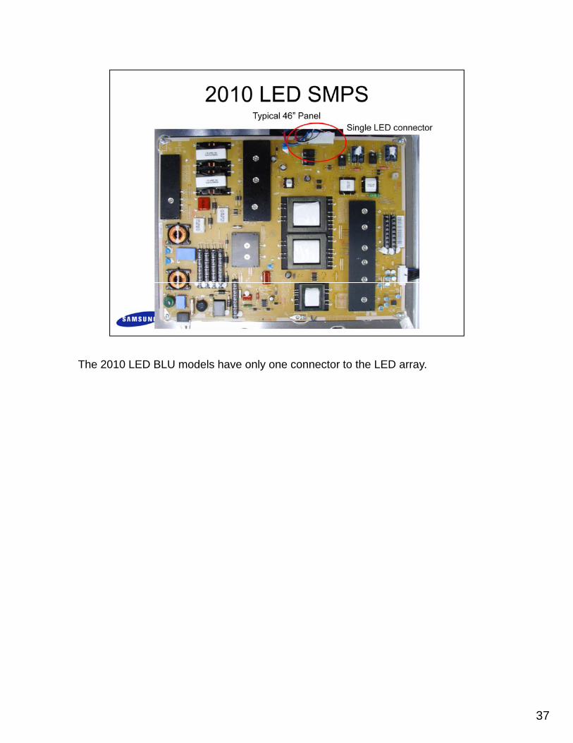
The 2010 LED BLU models have only one connector to the LED array.
37
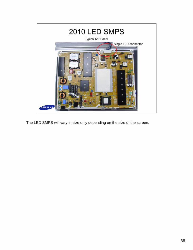
The LED SMPS will vary in size only depending on the size of the screen.
38

The LED Backlight is driven by approximately 170 volts from the power supply board. One side of the panel is driven by voltage at connector CN 9401 and the other side by the signal at CN9402. If one of the connectors is unplugged you may not notice a large brightness change depending on the scene being viewed. You can isolate the left or right side of the panel by swapping the connectors. If the one of the LED strips fails this means the panel must be replaced.
39

LCD TV’s using CCFL backlights use an inverter circuit to power the tubes. The inverter circuit uses a switch mode type power supply to up convert a low voltage to a high voltage. In most cases 20 to 24 Volts DC is applied to the primary of the transformer. Using step up transformer the voltage is raised to approximately 1000 Volts at startup. The control circuit regulates the run time voltage to approximately 500V. The switch mode supply is designed to oscillate at a frequency around 90KHz.
40

41
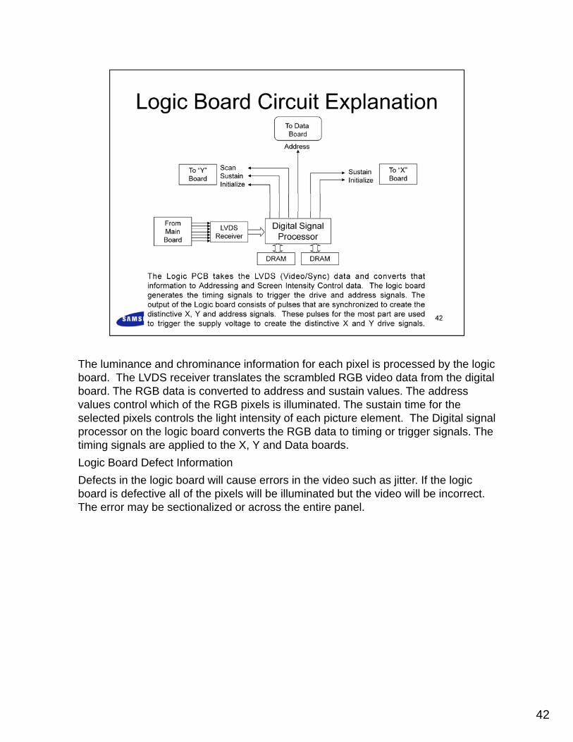
The luminance and chrominance information for each pixel is processed by the logic board. The LVDS receiver translates the scrambled RGB video data from the digital board. The RGB data is converted to address and sustain values. The address values control which of the RGB pixels is illuminated. The sustain time for the selected pixels controls the light intensity of each picture element. The Digital signal processor on the logic board converts the RGB data to timing or trigger signals. The timing signals are applied to the X, Y and Data boards. L i B d D f t I f tiLogic Board Defect InformationDefects in the logic board will cause errors in the video such as jitter. If the logic board is defective all of the pixels will be illuminated but the video will be incorrect. The error may be sectionalized or across the entire panel.
42

43
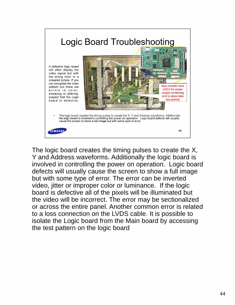
The logic board creates the timing pulses to create the X, g g p ,Y and Address waveforms. Additionally the logic board is involved in controlling the power on operation. Logic board defects will usually cause the screen to show a full image but with some type of error. The error can be inverted video, jitter or improper color or luminance. If the logic j p p gboard is defective all of the pixels will be illuminated but the video will be incorrect. The error may be sectionalized or across the entire panel. Another common error is related to a loss connection on the LVDS cable. It is possible to isolate the Logic board from the Main board by accessing the test pattern on the logic board
44

The normal operation LED will blink and the picture will be normal. If the defect LED starts to blink slowly and there is no picture, disconnect the LVDS cable, one at a time, from the “X”, “Y” and Address board until the normal operation LED starts blinking. The disconnected board that causes the normal operation LED to start blinking is defective.
45
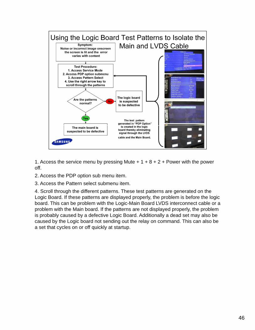
1. Access the service menu by pressing Mute + 1 + 8 + 2 + Power with the power off. 2. Access the PDP option sub menu item. 3. Access the Pattern select submenu item. 4. Scroll through the different patterns. These test patterns are generated on the Logic Board. If these patterns are displayed properly, the problem is before the logic board This can be problem with the Logic-Main Board LVDS interconnect cable or aboard. This can be problem with the Logic Main Board LVDS interconnect cable or a problem with the Main board. If the patterns are not displayed properly, the problem is probably caused by a defective Logic Board. Additionally a dead set may also be caused by the Logic board not sending out the relay on command. This can also be a set that cycles on or off quickly at startup.
46
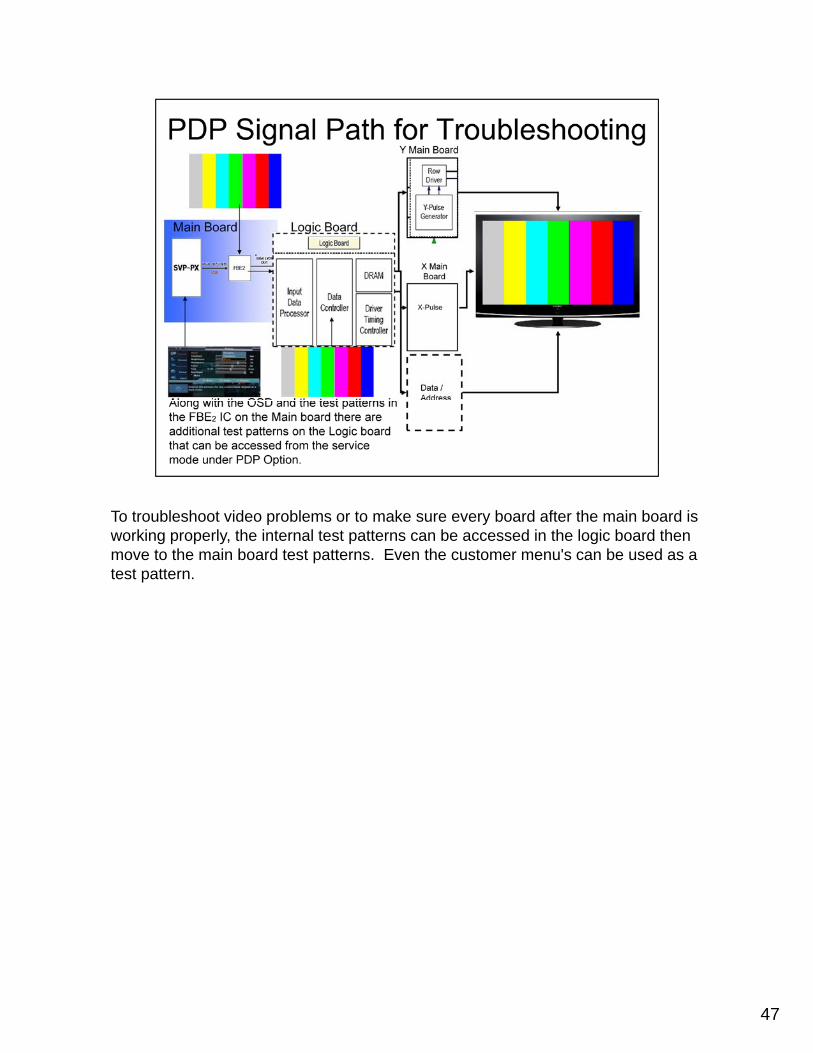
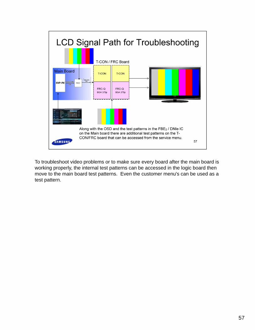
To troubleshoot video problems or to make sure every board after the main board is working properly, the internal test patterns can be accessed in the logic board then move to the main board test patterns. Even the customer menu's can be used as a test pattern.
47

The SMPS can be forced on and the test patterns that reside on the logic PCB can be displayed using this method. Before jumping the PS_ON to ground verify the connections in the service manual.
48

The patterns that will be displayed from the logic PCB are located after the LVDS cable. If the patterns look normal, the SMPS, logic, X, Y, buffers and panel are all working properly. Use this method in cases where the video is so distorted that the menus can not be seen to access the test patterns using the service mode.
49

The 2010 PDP SMPS varies slightly from the prior years in that there is a smaller connector from the SMPS to the main PCB. However the procedure for turning the SMPS on is the same. There may be a 12 pin connector or an 18 pin connector.
50
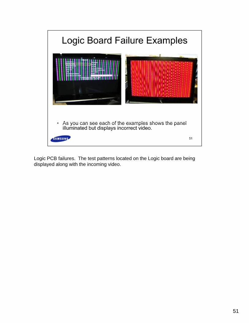
Logic PCB failures. The test patterns located on the Logic board are being displayed along with the incoming video.
51

Logic PCB failures. The test patterns located on the Logic board are being displayed along with the incoming video.
52
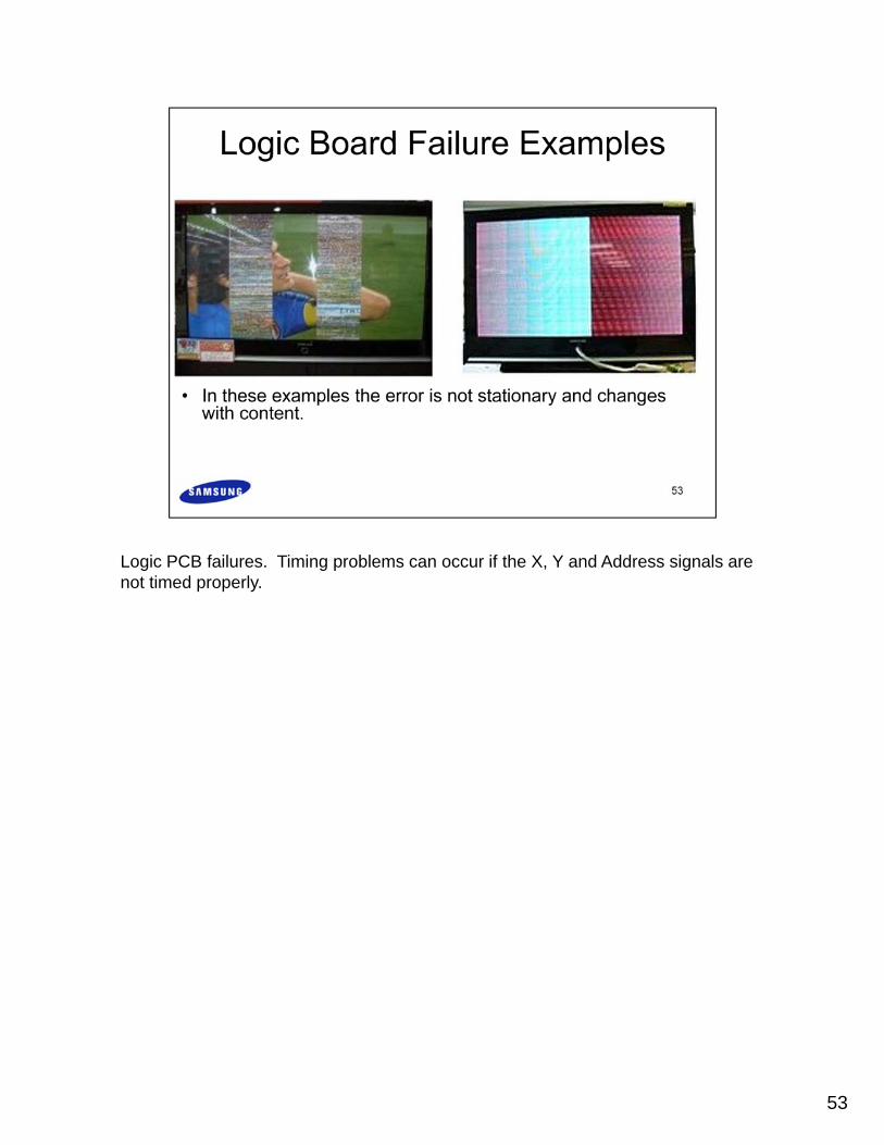
Logic PCB failures. Timing problems can occur if the X, Y and Address signals are not timed properly.
53
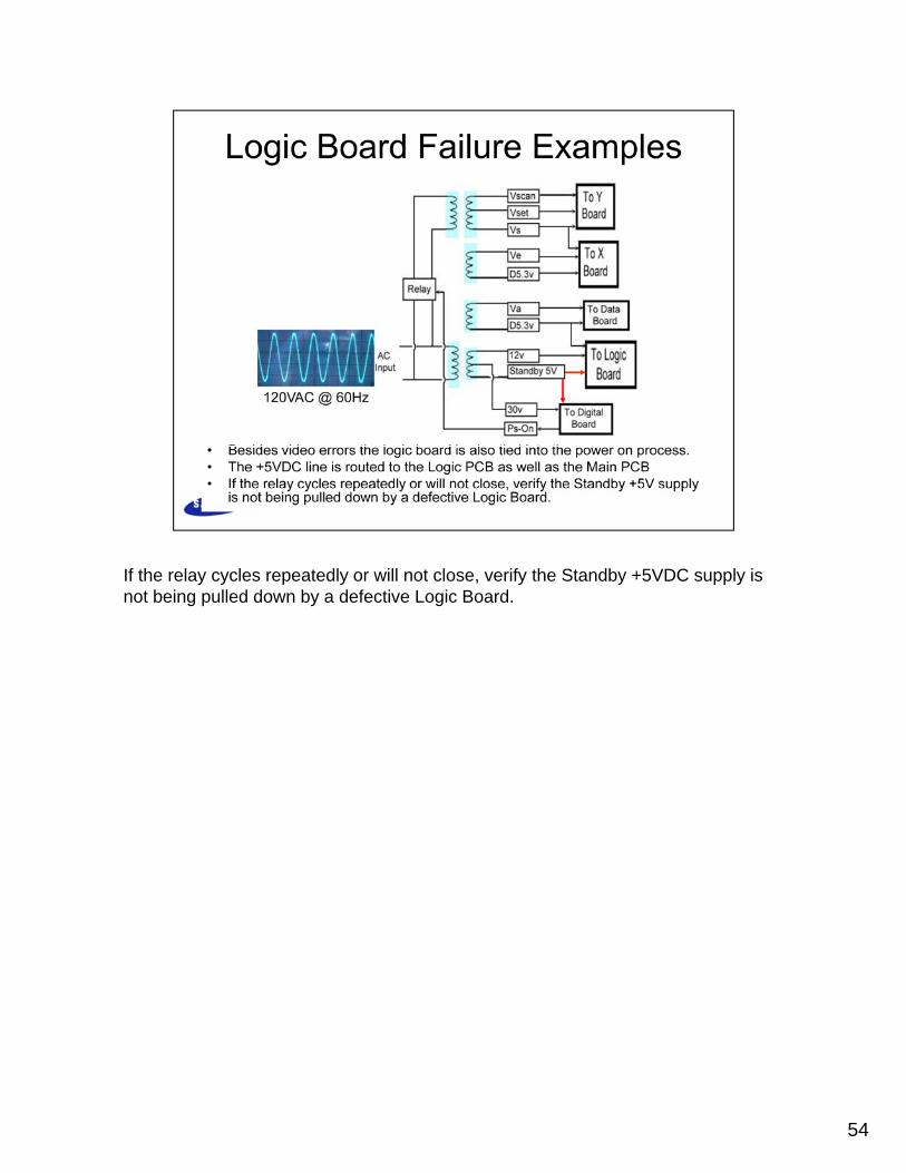
If the relay cycles repeatedly or will not close, verify the Standby +5VDC supply is not being pulled down by a defective Logic Board.
54
55

Once the video information has been converted to the correct resolution it is applied to the TCON Board. The TCON board selects the row and column that is supposed to be lit. The TCON Board also controls the duration that the sub pixel is lit. Information from the main PCB is fed to the TCON board via the LVDS cable. The encoded data is decoded by the LVDS receiver then fed to the row and column drivers. Selecting an individual sub pixel is accomplished by sending a row address pulse at the same time as the column address pulse. The two intersecting pulses cause the sub pixel to lightcause the sub pixel to light.
56
To troubleshoot video problems or to make sure every board after the main board is working properly, the internal test patterns can be accessed in the logic board then move to the main board test patterns. Even the customer menu's can be used as a test pattern.
57

T-Con board failures can be all over the screen or localized. TCON board failures can cause half the screen to go black or full white. TCON Board defects do not go away with content or connection. If the problem disappears when the input is changed it is not the TCON board. If the problem completely disappears with a darker or brighter scene the problem is not the TCON board.If the screen defect appears after a period of time the TCON board can be suspected.
58

Models that use 120Hz or 240Hz refresh rates use a combination TCON and FRC Board. FRC or frame rate conversion is where the extra frames are created or interpolated. Video in LVDS format is applied to the FRC board. The FRC board creates the additional frames by reading two adjacent original frames then calculating the luminance and chrominance data.
59
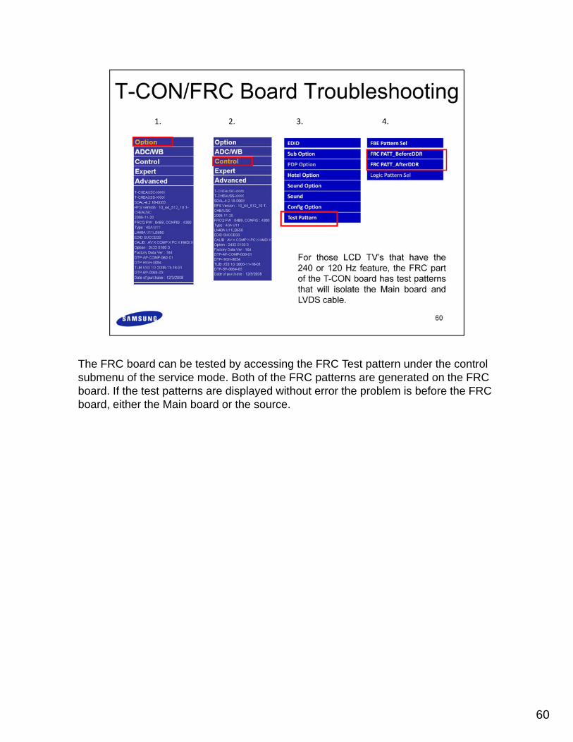
The FRC board can be tested by accessing the FRC Test pattern under the control submenu of the service mode. Both of the FRC patterns are generated on the FRC board. If the test patterns are displayed without error the problem is before the FRC board, either the Main board or the source.
60
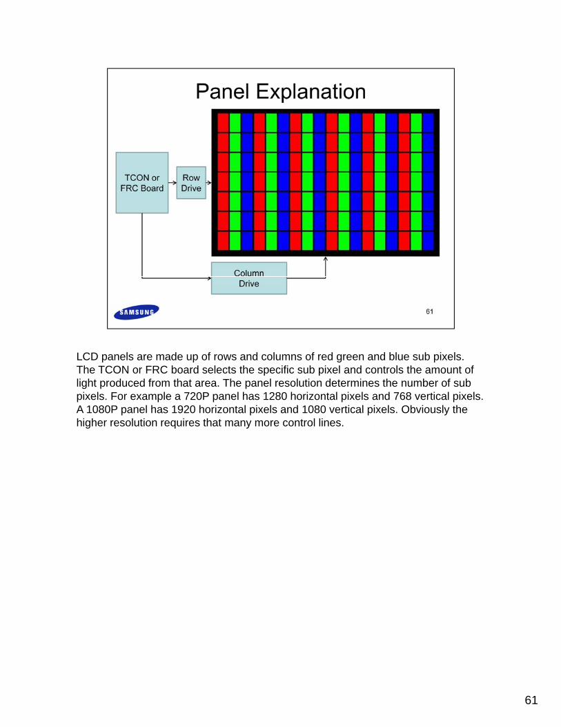
LCD panels are made up of rows and columns of red green and blue sub pixels. The TCON or FRC board selects the specific sub pixel and controls the amount of light produced from that area. The panel resolution determines the number of sub pixels. For example a 720P panel has 1280 horizontal pixels and 768 vertical pixels. A 1080P panel has 1920 horizontal pixels and 1080 vertical pixels. Obviously the higher resolution requires that many more control lines.
61

62
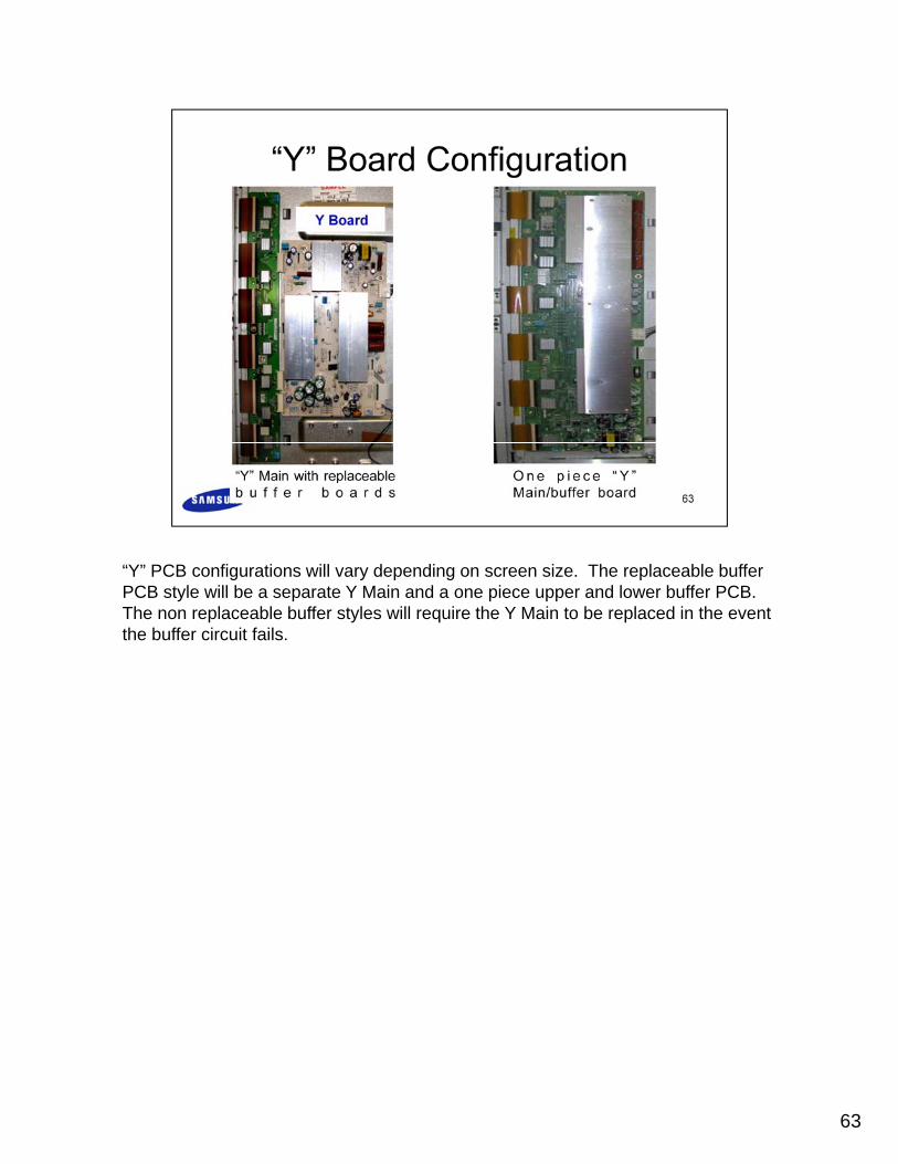
“Y” PCB configurations will vary depending on screen size. The replaceable buffer PCB style will be a separate Y Main and a one piece upper and lower buffer PCB. The non replaceable buffer styles will require the Y Main to be replaced in the event the buffer circuit fails.
63
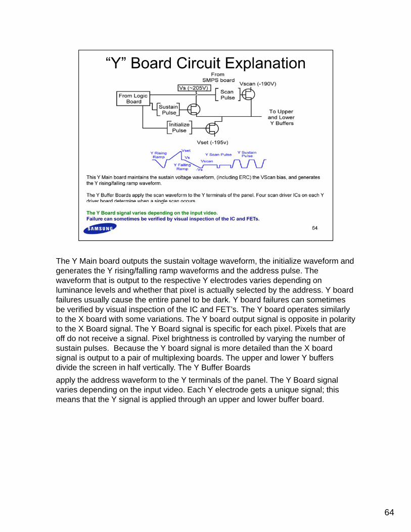
The Y Main board outputs the sustain voltage waveform, the initialize waveform and generates the Y rising/falling ramp waveforms and the address pulse. The waveform that is output to the respective Y electrodes varies depending on luminance levels and whether that pixel is actually selected by the address. Y board failures usually cause the entire panel to be dark. Y board failures can sometimes be verified by visual inspection of the IC and FET’s. The Y board operates similarly to the X board with some variations. The Y board output signal is opposite in polarity to the X Board signal The Y Board signal is specific for each pixel Pixels that areto the X Board signal. The Y Board signal is specific for each pixel. Pixels that are off do not receive a signal. Pixel brightness is controlled by varying the number of sustain pulses. Because the Y board signal is more detailed than the X board signal is output to a pair of multiplexing boards. The upper and lower Y buffers divide the screen in half vertically. The Y Buffer Boards apply the address waveform to the Y terminals of the panel. The Y Board signal varies depending on the input video. Each Y electrode gets a unique signal; this p g p g q g ;means that the Y signal is applied through an upper and lower buffer board.
64
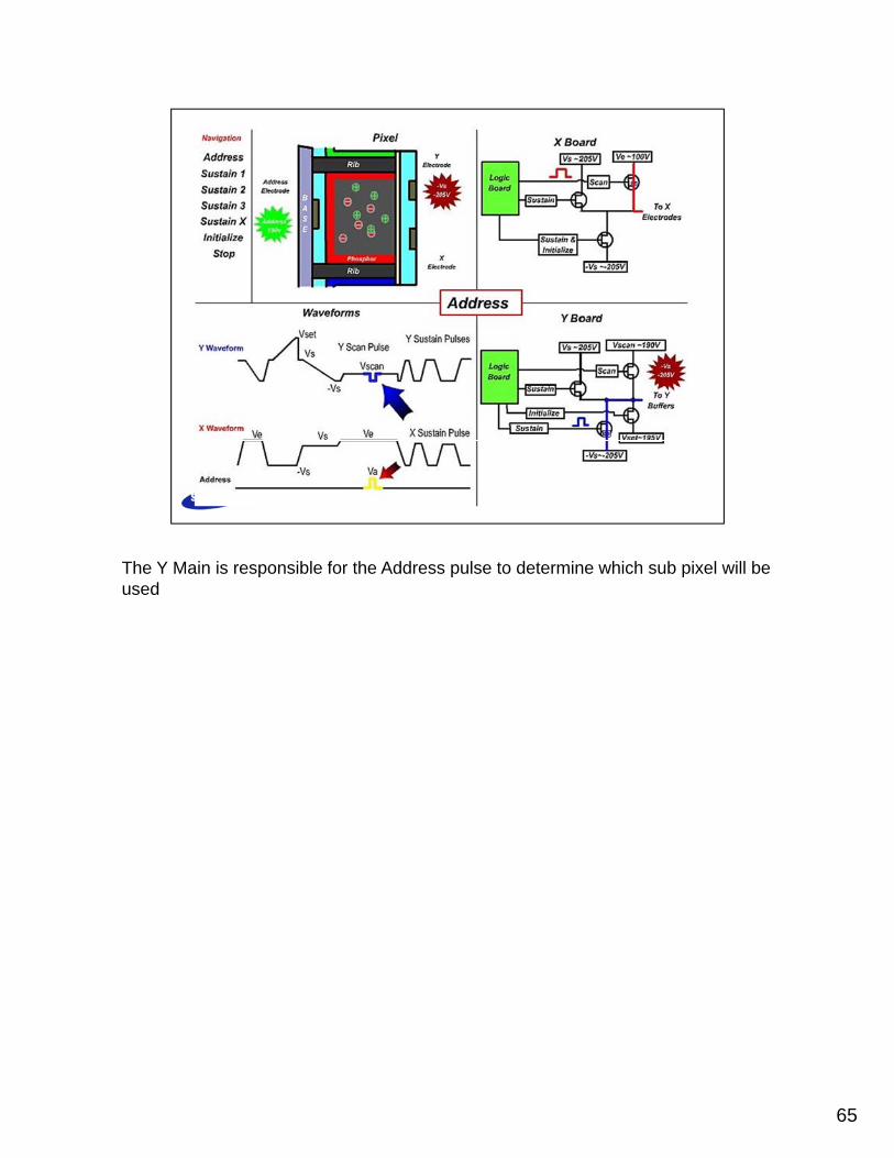
The Y Main is responsible for the Address pulse to determine which sub pixel will be used
65
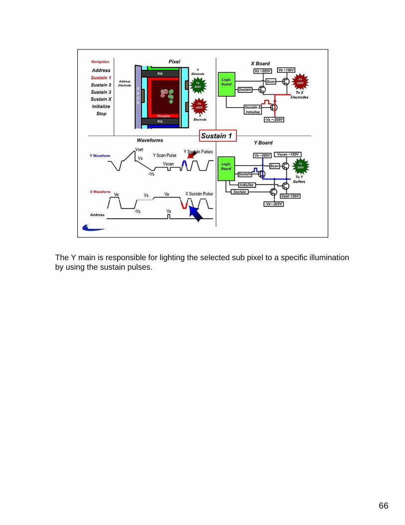
The Y main is responsible for lighting the selected sub pixel to a specific illumination by using the sustain pulses.
66
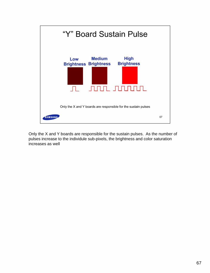
Only the X and Y boards are responsible for the sustain pulses. As the number of pulses increase to the individule sub-pixels, the brightness and color saturation increases as well
67
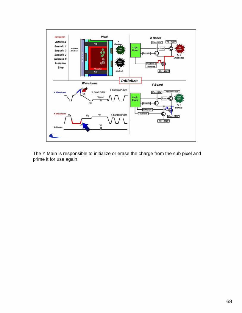
The Y Main is responsible to initialize or erase the charge from the sub pixel and prime it for use again.
68
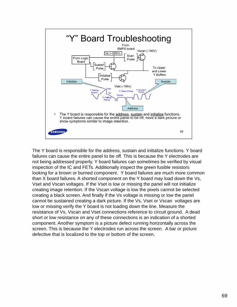
The Y board is responsible for the address, sustain and initialize functions. Y board failures can cause the entire panel to be off. This is because the Y electrodes are not being addressed properly. Y board failures can sometimes be verified by visual inspection of the IC and FETs. Additionally inspect the green fusible resistors looking for a brown or burned component. Y board failures are much more common than X board failures. A shorted component on the Y board may load down the Vs, Vset and Vscan voltages. If the Vset is low or missing the panel will not initialize creating image retention If the Vscan voltage is low the pixels cannot be selectedcreating image retention. If the Vscan voltage is low the pixels cannot be selected creating a black screen. And finally if the Vs voltage is missing or low the panel cannot be sustained creating a dark picture. If the Vs, Vset or Vscan voltages are low or missing verify the Y board is not loading down the line. Measure the resistance of Vs, Vscan and Vset connections reference to circuit ground. A dead short or low resistance on any of these connections is an indication of a shorted component. Another symptom is a picture defect running horizontally across the screen. This is because the Y electrodes run across the screen. A bar or picture defective that is localized to the top or bottom of the screen.
69

The Y board is responsible for the address, sustain and initialize functions. Y board failures can cause the entire panel to be off. This is because the Y electrodes are not being addressed properly. Y board failures can sometimes be verified by visual inspection of the IC and FETs. Additionally inspect the green fusible resistors looking for a brown or burned component. Y board failures are much more common than X board failures. A shorted component on the Y board may load down the Vs, Vset and Vscan voltages. If the Vset is low or missing the panel will not initialize creating image retention If the Vscan voltage is low the pixels cannot be selectedcreating image retention. If the Vscan voltage is low the pixels cannot be selected creating a black screen. And finally if the Vs voltage is missing or low the panel cannot be sustained creating a dark picture. If the Vs, Vset or Vscan voltages are low or missing verify the Y board is not loading down the line. Measure the resistance of Vs, Vscan and Vset connections reference to circuit ground. A dead short or low resistance on any of these connections is an indication of a shorted component. Another symptom is a picture defect running horizontally across the screen. This is because the Y electrodes run across the screen. A bar or picture defective that is localized to the top or bottom of the screen.
70

The Y board is responsible for the address, sustain and initialize functions. Y board failures can cause the entire panel to be off. This is because the Y electrodes are not being addressed properly. Y board failures can sometimes be verified by visual inspection of the IC and FETs. Additionally inspect the green fusible resistors looking for a brown or burned component. Y board failures are much more common than X board failures. A shorted component on the Y board may load down the Vs, Vset and Vscan voltages. If the Vset is low or missing the panel will not initialize creating image retention If the Vscan voltage is low the pixels cannot be selectedcreating image retention. If the Vscan voltage is low the pixels cannot be selected creating a black screen. And finally if the Vs voltage is missing or low the panel cannot be sustained creating a dark picture. If the Vs, Vset or Vscan voltages are low or missing verify the Y board is not loading down the line. Measure the resistance of Vs, Vscan and Vset connections reference to circuit ground. A dead short or low resistance on any of these connections is an indication of a shorted component. Another symptom is a picture defect running horizontally across the screen. This is because the Y electrodes run across the screen. A bar or picture defective that is localized to the top or bottom of the screen.
71
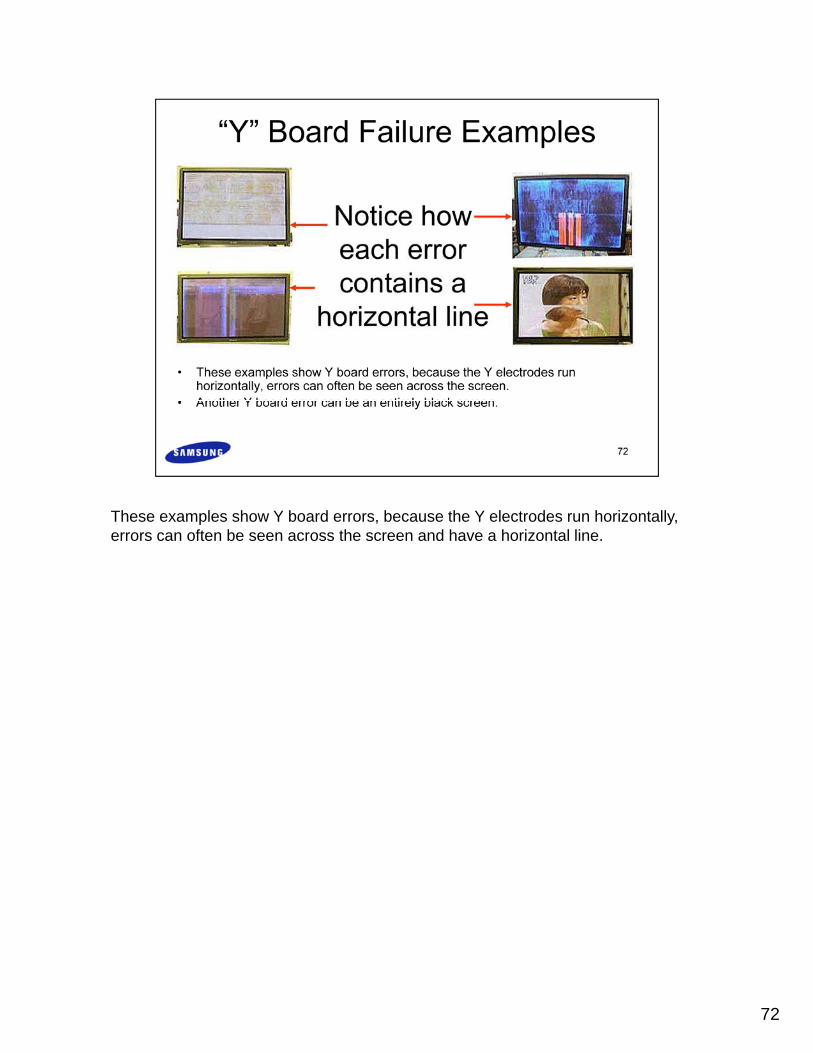
These examples show Y board errors, because the Y electrodes run horizontally, errors can often be seen across the screen and have a horizontal line.
72

The Y board is responsible for the address, sustain and initialize functions. Y board failures can cause the entire panel to be off. This is because the Y electrodes are not being addressed properly. Y board failures can sometimes be verified by visual inspection of the IC and FETs. Additionally inspect the green fusible resistors looking for a brown or burned component. Y board failures are much more common than X board failures. A shorted component on the Y board may load down the Vs, Vset and Vscan voltages. If the Vset is low or missing the panel will not initialize creating image retention If the Vscan voltage is low the pixels cannot be selectedcreating image retention. If the Vscan voltage is low the pixels cannot be selected creating a black screen. And finally if the Vs voltage is missing or low the panel cannot be sustained creating a dark picture. If the Vs, Vset or Vscan voltages are low or missing verify the Y board is not loading down the line. Measure the resistance of Vs, Vscan and Vset connections reference to circuit ground. A dead short or low resistance on any of these connections is an indication of a shorted component. Another symptom is a picture defect running horizontally across the screen. This is because the Y electrodes run across the screen. A bar or picture defective that is localized to the top or bottom of the screen.
73
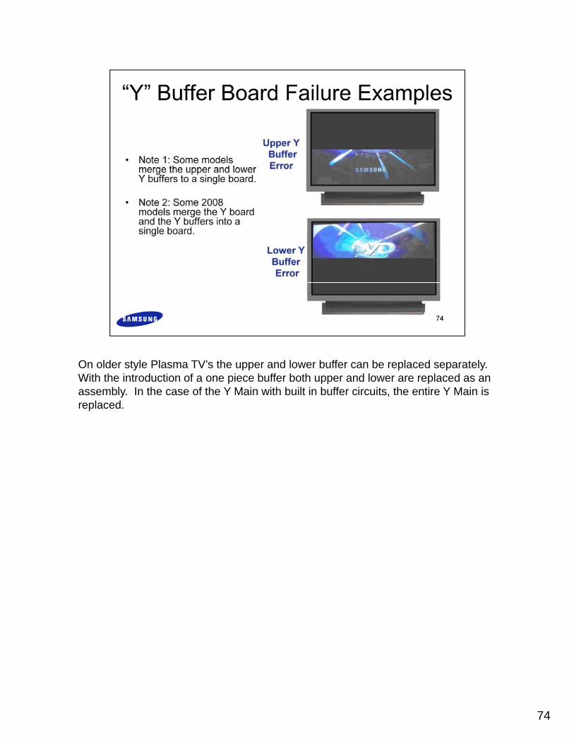
On older style Plasma TV’s the upper and lower buffer can be replaced separately. With the introduction of a one piece buffer both upper and lower are replaced as an assembly. In the case of the Y Main with built in buffer circuits, the entire Y Main is replaced.
74

The connection between the buffer and the panel can cause these types of problems. The connections can be cleaned and reseated but make sure the power is removed before attempting. To avoid buffer connector problems some models may have the panel ribbon cable attached directly to the buffer and is part of the panel.
75

76
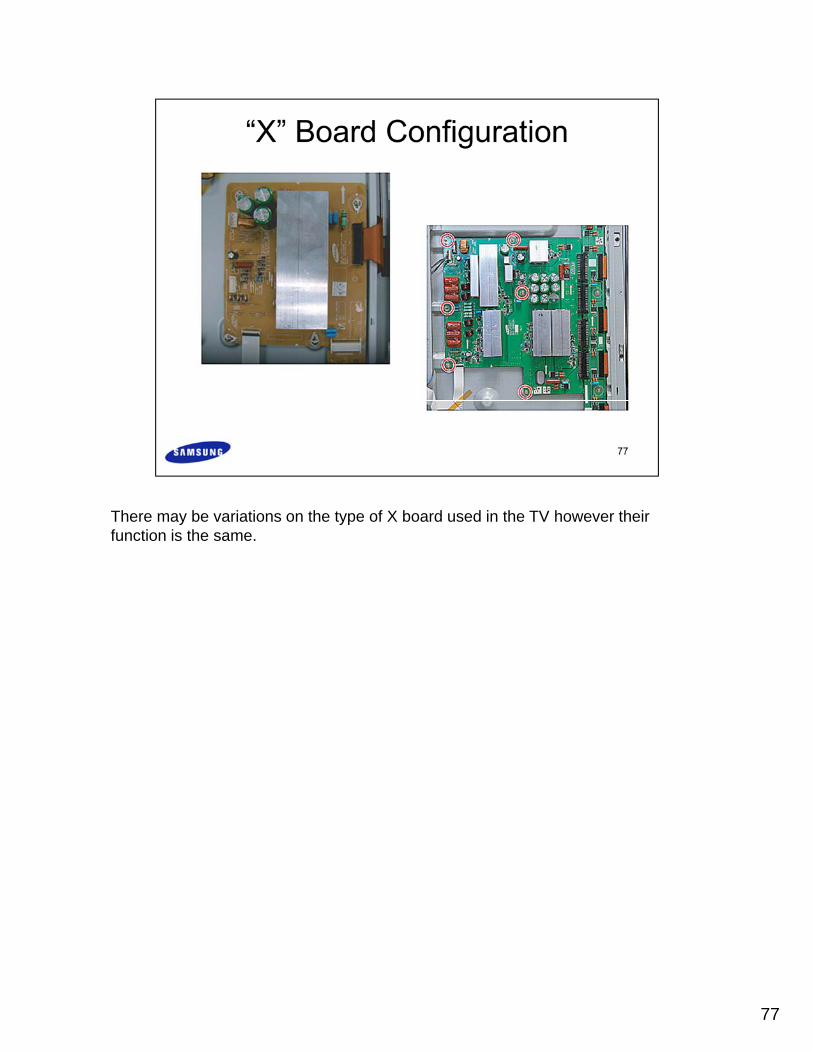
There may be variations on the type of X board used in the TV however their function is the same.
77
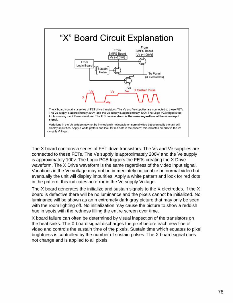
The X board contains a series of FET drive transistors. The Vs and Ve supplies are connected to these FETs. The Vs supply is approximately 200V and the Ve supply is approximately 100v. The Logic PCB triggers the FETs creating the X Drive waveform. The X Drive waveform is the same regardless of the video input signal. Variations in the Ve voltage may not be immediately noticeable on normal video but eventually the unit will display impurities. Apply a white pattern and look for red dots in the pattern, this indicates an error in the Ve supply Voltage. Th X b d t th i iti li d t i i l t th X l t d If th XThe X board generates the initialize and sustain signals to the X electrodes. If the X board is defective there will be no luminance and the pixels cannot be initialized. No luminance will be shown as an n extremely dark gray picture that may only be seen with the room lighting off. No initialization may cause the picture to show a reddish hue in spots with the redness filling the entire screen over time.X board failure can often be determined by visual inspection of the transistors on the heat sinks The X board signal discharges the pixel before each new line ofthe heat sinks. The X board signal discharges the pixel before each new line of video and controls the sustain time of the pixels. Sustain time which equates to pixel brightness is controlled by the number of sustain pulses. The X board signal does not change and is applied to all pixels.
78
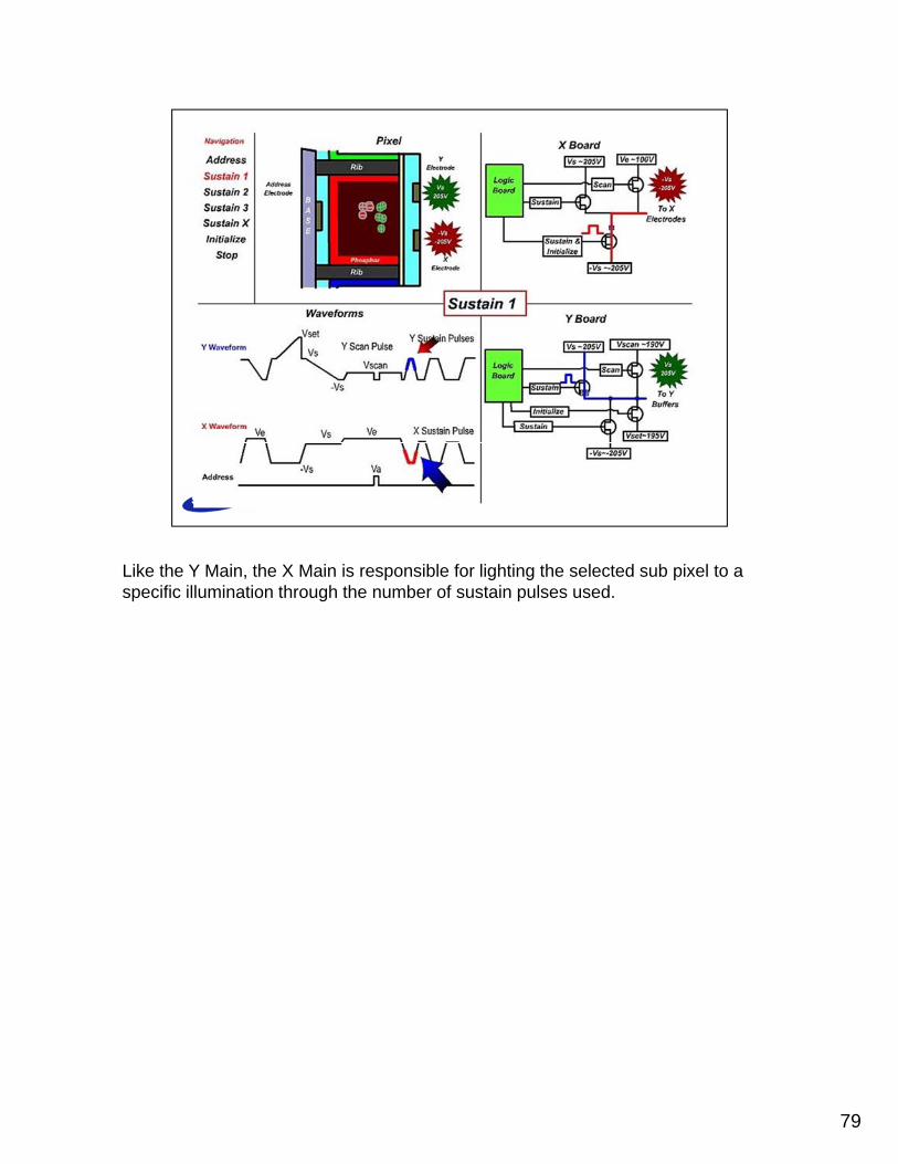
Like the Y Main, the X Main is responsible for lighting the selected sub pixel to a specific illumination through the number of sustain pulses used.
79
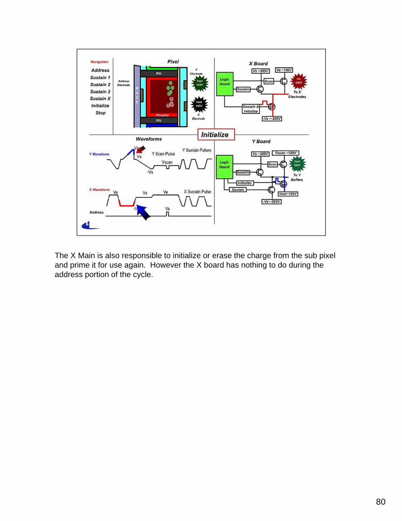
The X Main is also responsible to initialize or erase the charge from the sub pixel and prime it for use again. However the X board has nothing to do during the address portion of the cycle.
80
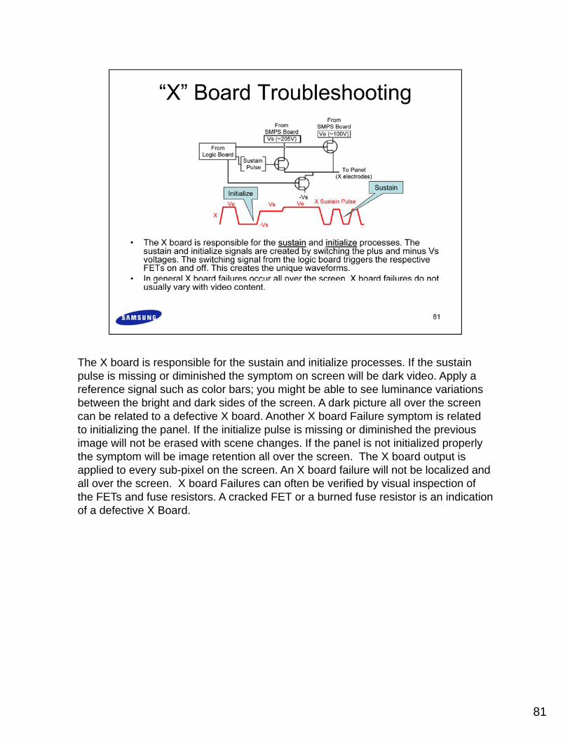
The X board is responsible for the sustain and initialize processes. If the sustain pulse is missing or diminished the symptom on screen will be dark video. Apply a reference signal such as color bars; you might be able to see luminance variations between the bright and dark sides of the screen. A dark picture all over the screen can be related to a defective X board. Another X board Failure symptom is related to initializing the panel. If the initialize pulse is missing or diminished the previous image will not be erased with scene changes. If the panel is not initialized properly the symptom will be image retention all over the screen The X board output isthe symptom will be image retention all over the screen. The X board output is applied to every sub-pixel on the screen. An X board failure will not be localized and all over the screen. X board Failures can often be verified by visual inspection of the FETs and fuse resistors. A cracked FET or a burned fuse resistor is an indication of a defective X Board.
81
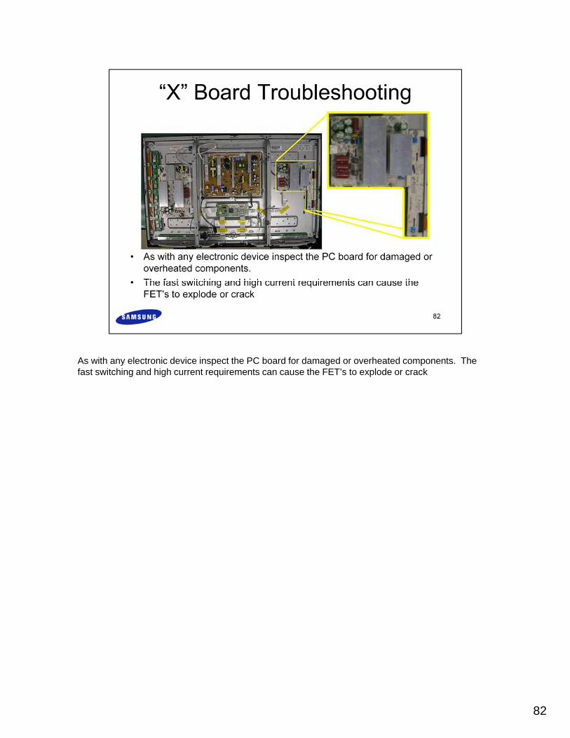
As with any electronic device inspect the PC board for damaged or overheated components. The f t it hi d hi h t i t th FET’ t l d kfast switching and high current requirements can cause the FET’s to explode or crack
82
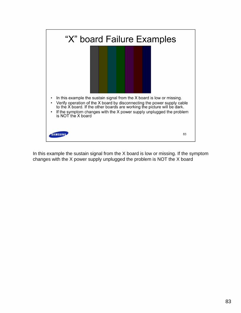
In this example the sustain signal from the X board is low or missing. If the symptom changes with the X power supply unplugged the problem is NOT the X board
83
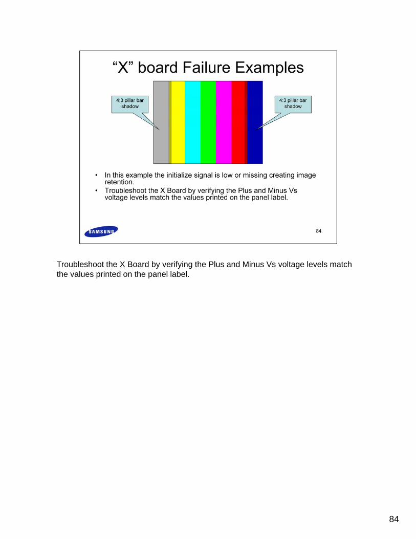
Troubleshoot the X Board by verifying the Plus and Minus Vs voltage levels match the values printed on the panel label.
84

85
86

The addition of a
87
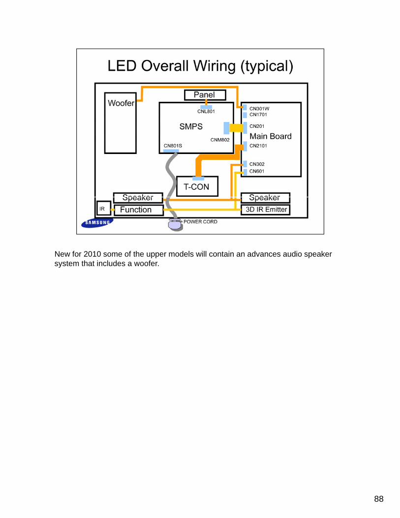
New for 2010 some of the upper models will contain an advances audio speaker system that includes a woofer.
88

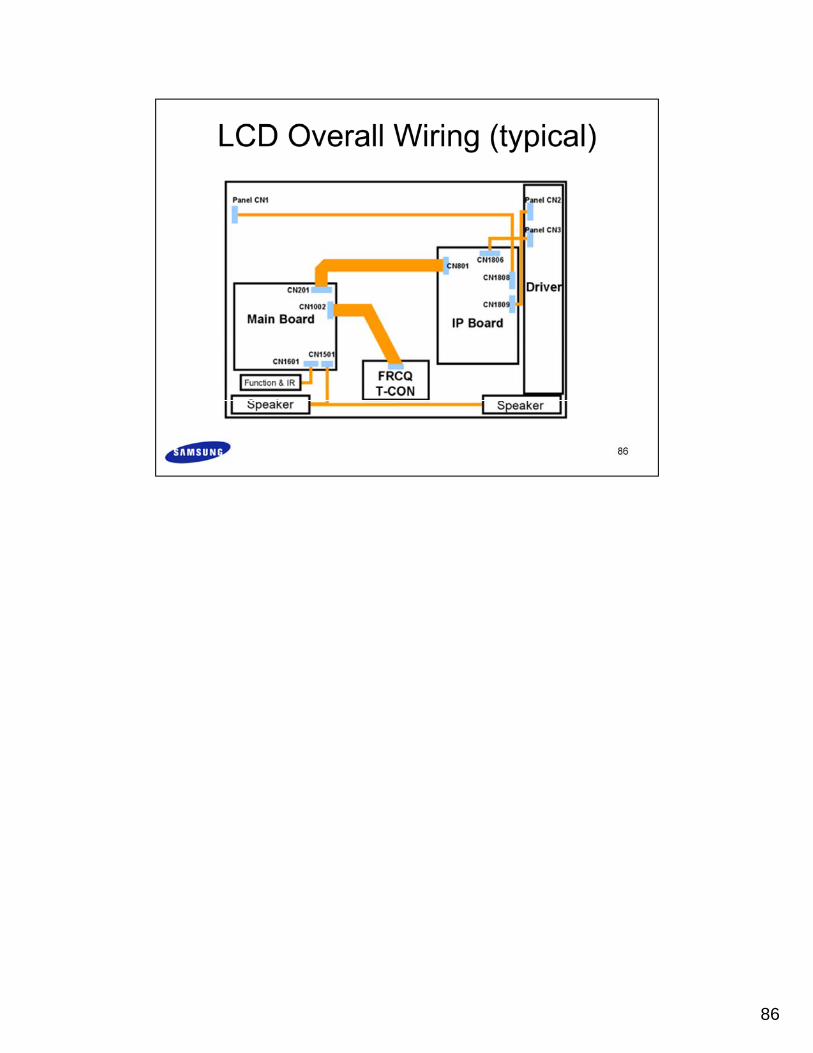
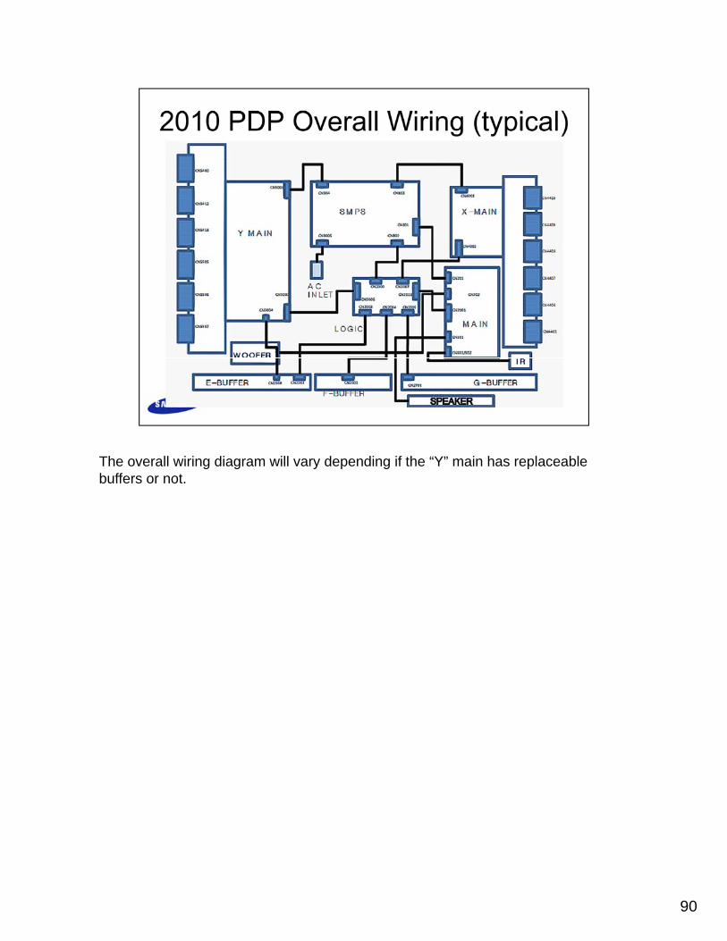
The overall wiring diagram will vary depending if the “Y” main has replaceable buffers or not.
89
The overall wiring diagram will vary depending if the “Y” main has replaceable buffers or not.
90
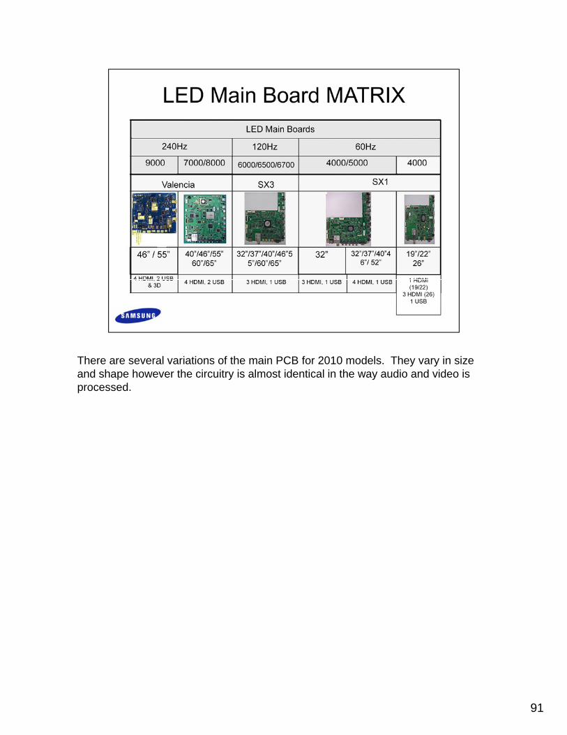
There are several variations of the main PCB for 2010 models. They vary in size and shape however the circuitry is almost identical in the way audio and video is processed.
91
There are several variations of the main PCB for 2010 models. They vary in size and shape however the circuitry is almost identical in the way audio and video is processed.
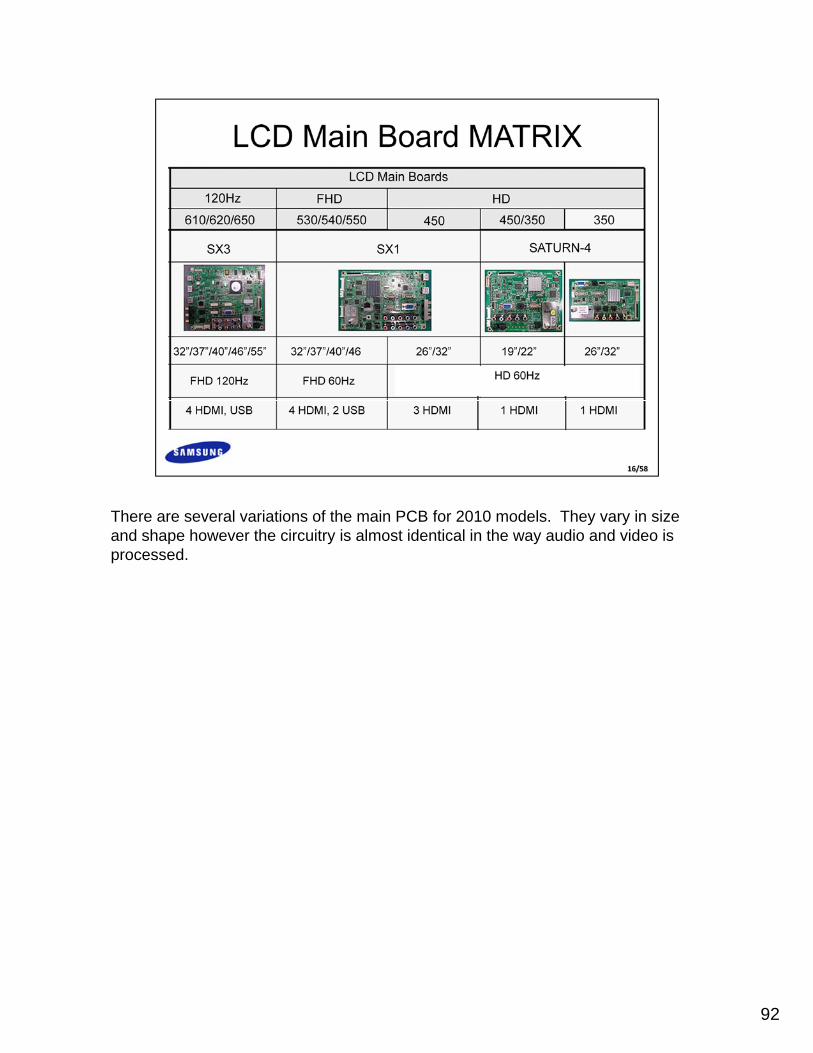
92

There are several variations of the main PCB for 2010 models. They vary in size and shape however the circuitry is almost identical in the way audio and video is processed.
93
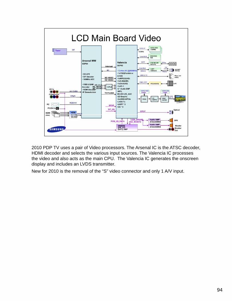
2010 PDP TV uses a pair of Video processors. The Arsenal IC is the ATSC decoder, HDMI decoder and selects the various input sources. The Valencia IC processes the video and also acts as the main CPU. The Valencia IC generates the onscreen display and includes an LVDS transmitter.New for 2010 is the removal of the “S” video connector and only 1 A/V input.
94
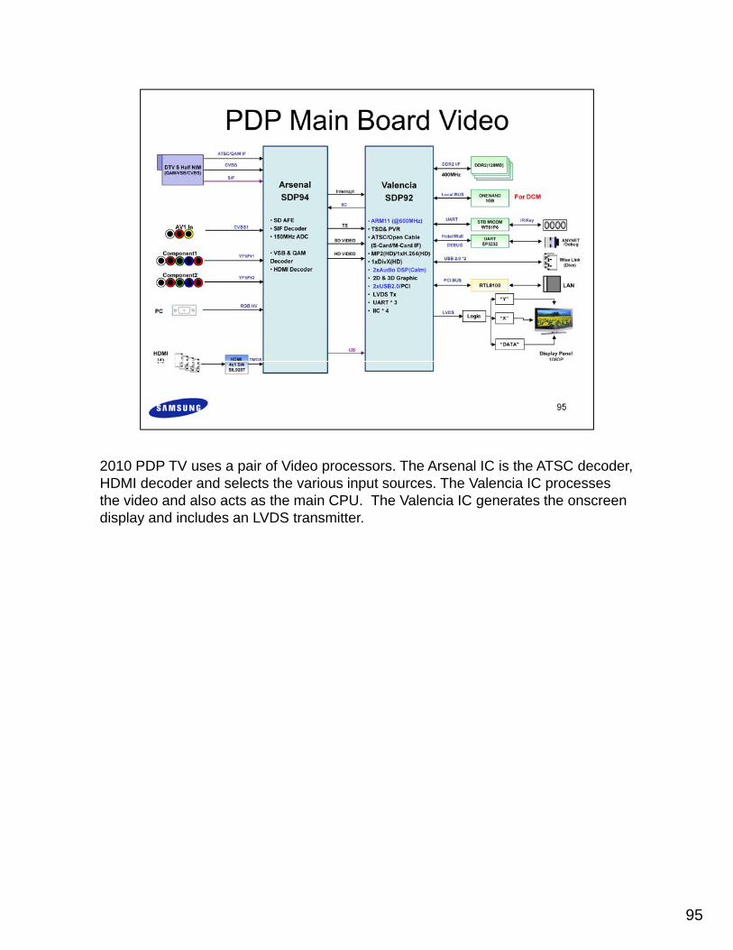
2010 PDP TV uses a pair of Video processors. The Arsenal IC is the ATSC decoder, HDMI decoder and selects the various input sources. The Valencia IC processes the video and also acts as the main CPU. The Valencia IC generates the onscreen display and includes an LVDS transmitter.
95
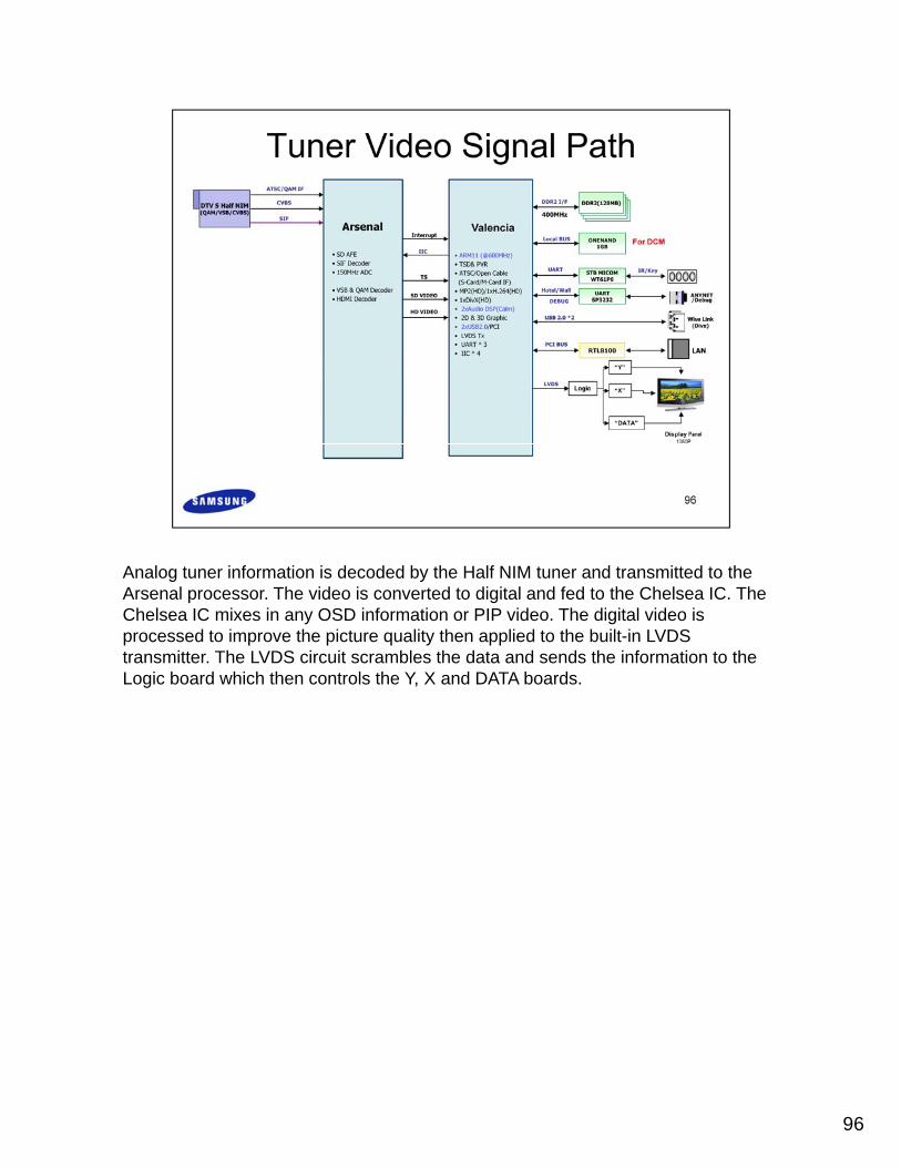
Analog tuner information is decoded by the Half NIM tuner and transmitted to the Arsenal processor. The video is converted to digital and fed to the Chelsea IC. The Chelsea IC mixes in any OSD information or PIP video. The digital video is processed to improve the picture quality then applied to the built-in LVDS transmitter. The LVDS circuit scrambles the data and sends the information to the Logic board which then controls the Y, X and DATA boards.
96
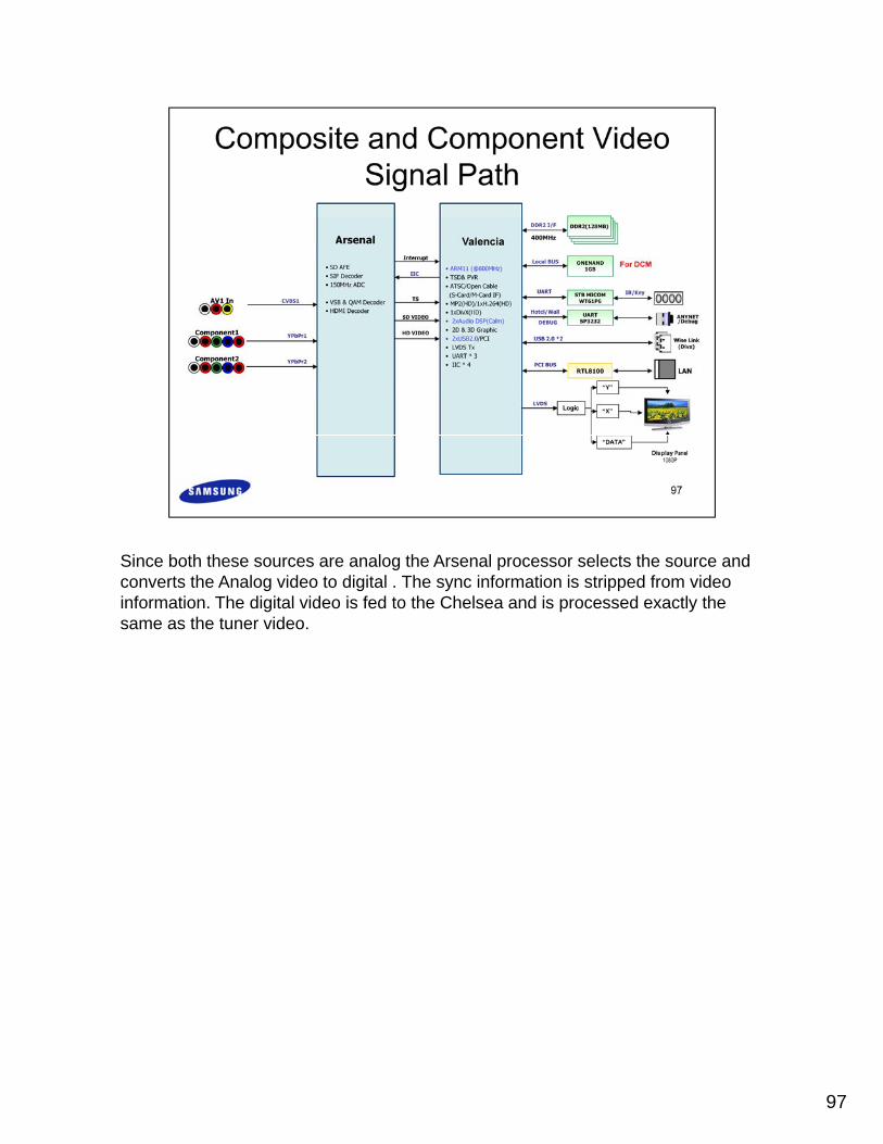
Since both these sources are analog the Arsenal processor selects the source and converts the Analog video to digital . The sync information is stripped from video information. The digital video is fed to the Chelsea and is processed exactly the same as the tuner video.
97
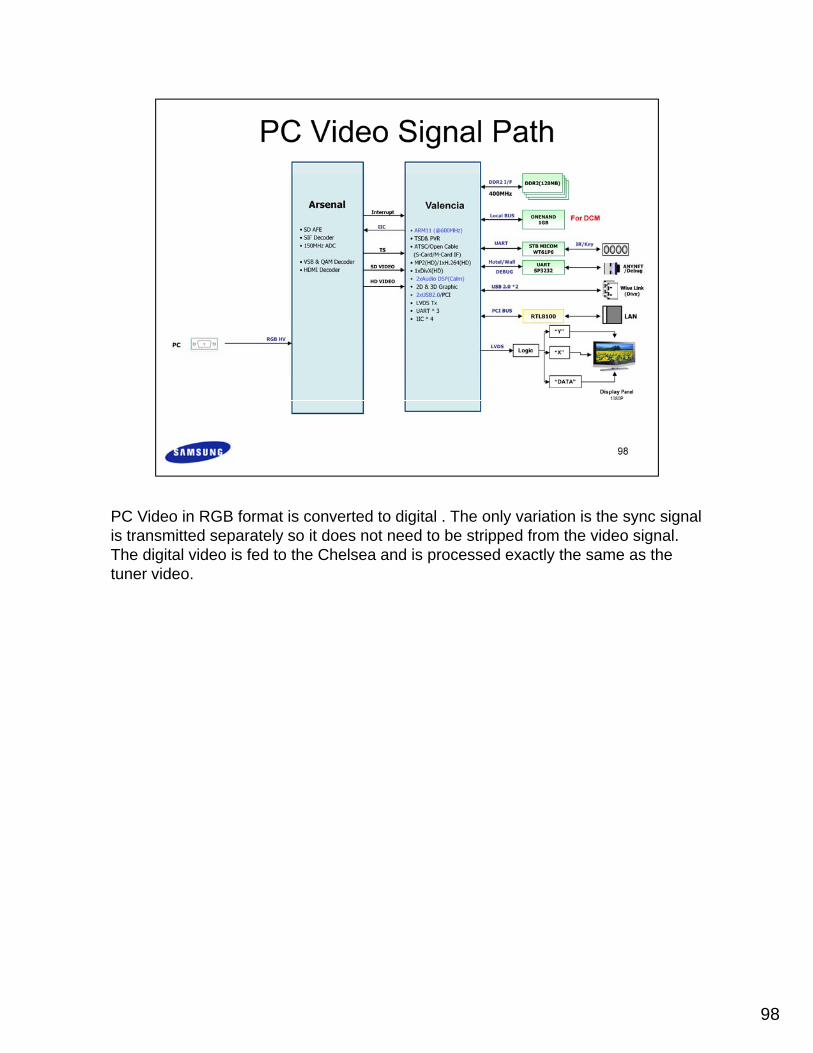
PC Video in RGB format is converted to digital . The only variation is the sync signal is transmitted separately so it does not need to be stripped from the video signal. The digital video is fed to the Chelsea and is processed exactly the same as the tuner video.
98

The Arsenal IC selects one of the 4 HDMI inputs. Since this signal is digital no conversion is required however the Arsenal IC does verify the content conforms to HDCP format. The video signal is stripped from the data stream and fed to the Chelsea IC. From here the process is exactly the same.
99
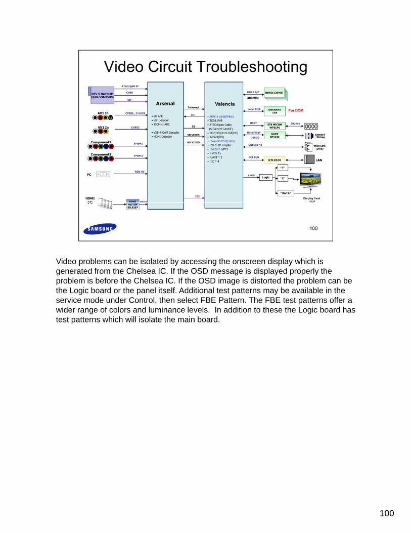
Video problems can be isolated by accessing the onscreen display which is generated from the Chelsea IC. If the OSD message is displayed properly the problem is before the Chelsea IC. If the OSD image is distorted the problem can be the Logic board or the panel itself. Additional test patterns may be available in the service mode under Control, then select FBE Pattern. The FBE test patterns offer a wider range of colors and luminance levels. In addition to these the Logic board has test patterns which will isolate the main board.
100

The main board also provides the operating system. This means all operation functions are controlled by this board.Main board failures can be specific to a single input or all sources. Access the Onscreen display to generate a reference picture that can be used to verify the operation of the Video processor. If the OSD image is correct in all aspects the source video is suspected. Main board problems can often be disguised by a defective or improperly connected LVDS cable. This cable transfers the video in di it l f t t th T CON b d I ti h i idigital format to the T-CON board. Improper connections here can cause missing data bits which will show a wide range of symptoms. Use the logic board test patterns to verify the problem is after the main board or before.
101
The main board also provides the operating system. This means all operation functions are controlled by this board.Main board failures can be specific to a single input or all sources. Access the Onscreen display to generate a reference picture that can be used to verify the operation of the Video processor. If the OSD image is correct in all aspects the source video is suspected. Main board problems can often be disguised by a defective or improperly connected LVDS cable. This cable transfers the video in di it l f t t th T CON b d I ti h i idigital format to the T-CON board. Improper connections here can cause missing data bits which will show a wide range of symptoms. Use the logic board test patterns to verify the problem is after the main board or before.
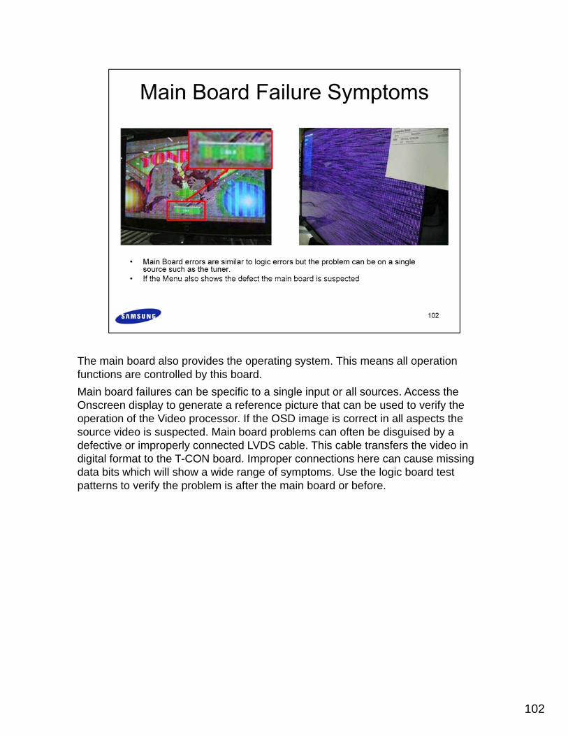
102
The main board also provides the operating system. This means all operation functions are controlled by this board.Main board failures can be specific to a single input or all sources. Access the Onscreen display to generate a reference picture that can be used to verify the operation of the Video processor. If the OSD image is correct in all aspects the source video is suspected. Main board problems can often be disguised by a defective or improperly connected LVDS cable. This cable transfers the video in di it l f t t th T CON b d I ti h i idigital format to the T-CON board. Improper connections here can cause missing data bits which will show a wide range of symptoms. Use the logic board test patterns to verify the problem is after the main board or before.
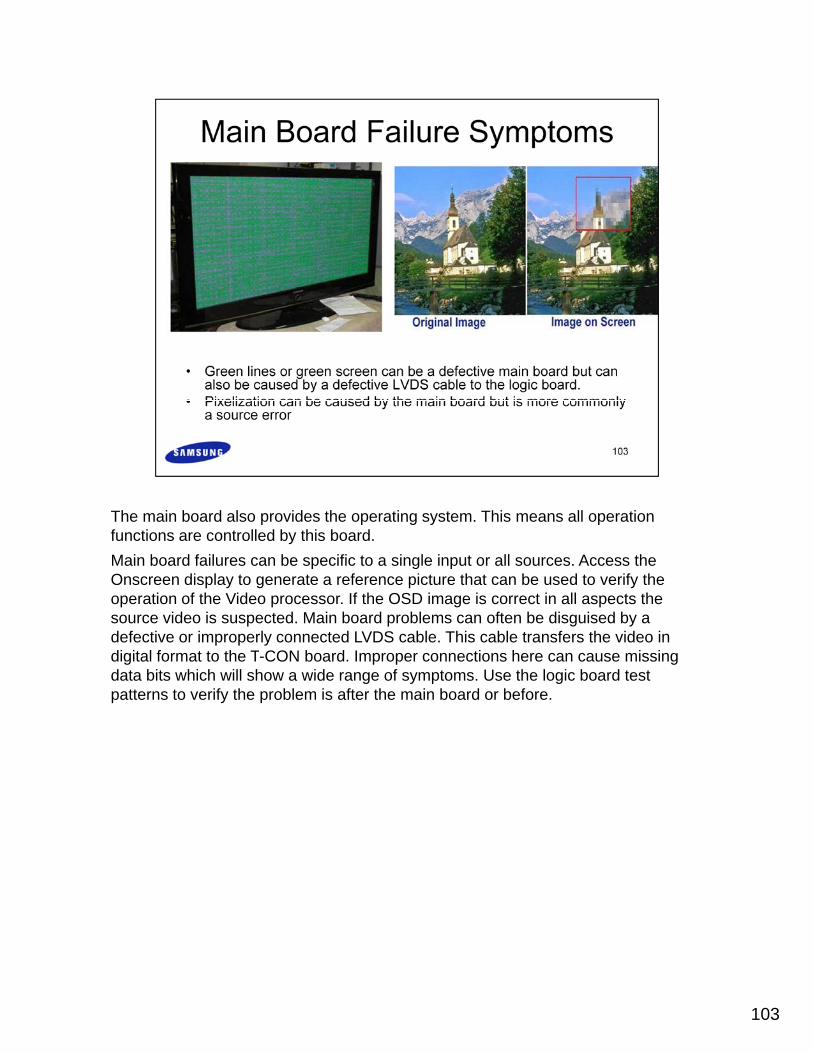
103
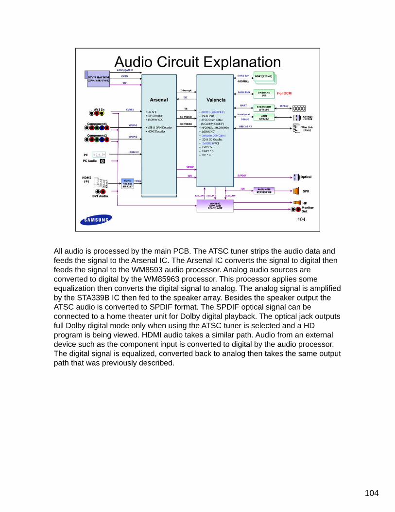
All audio is processed by the main PCB. The ATSC tuner strips the audio data and feeds the signal to the Arsenal IC. The Arsenal IC converts the signal to digital then feeds the signal to the WM8593 audio processor. Analog audio sources are converted to digital by the WM85963 processor. This processor applies some equalization then converts the digital signal to analog. The analog signal is amplified by the STA339B IC then fed to the speaker array. Besides the speaker output the ATSC audio is converted to SPDIF format. The SPDIF optical signal can be connected to a home theater unit for Dolby digital playback The optical jack outputsconnected to a home theater unit for Dolby digital playback. The optical jack outputs full Dolby digital mode only when using the ATSC tuner is selected and a HD program is being viewed. HDMI audio takes a similar path. Audio from an external device such as the component input is converted to digital by the audio processor. The digital signal is equalized, converted back to analog then takes the same output path that was previously described.
104
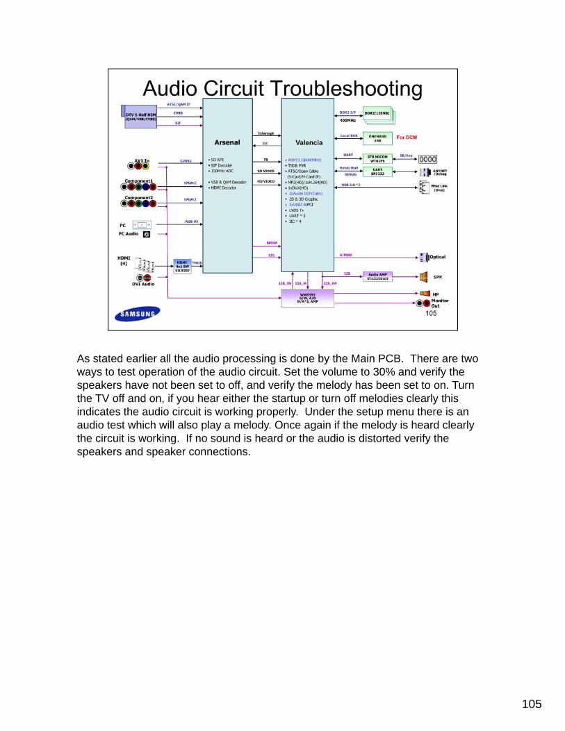
As stated earlier all the audio processing is done by the Main PCB. There are two ways to test operation of the audio circuit. Set the volume to 30% and verify the speakers have not been set to off, and verify the melody has been set to on. Turn the TV off and on, if you hear either the startup or turn off melodies clearly this indicates the audio circuit is working properly. Under the setup menu there is an audio test which will also play a melody. Once again if the melody is heard clearly the circuit is working. If no sound is heard or the audio is distorted verify the speakers and speaker connectionsspeakers and speaker connections.
105

In many cases on the new Plasma televisions, the data boards are not replaceable. If there is a failure the panel will require replacement.
106

107

A panel defect similar to the example here is caused by damage to the vacuum port on the side. Individual pixel failure does not necessarily require panel replacement. The table below shows the pixel specification. As you can see depending on the screen size and number of defective pixels determine if the product is covered by warranty.
108

Traditional LCD TV’s use a series of Fluorescent tubes for backlights. These tubes use high voltage and a phosphor coating to generate light . The FL tubes and circuitry behind the panel increases the depth of the rear cabinet
109

The Led's are arranged on the perimeter of the panel assembly. The individual Led's are connected in series with two sets of LEDS, one for each side of the screen. The back of the panel uses three reflective layers and unique lens assembly that distribute the light across the entire panel. Three benefits are smaller size, a simplified power supply and less power consumption.
110

Vertical or horizontal lines that are present with all inputs and all types of content are usually defective panels. Backlight errors can usually be identified by an area that is always noticeably darker. Smaller lines or imperfections in the image that are present in all modes is called de-lamination which requires replacing the panel.
111
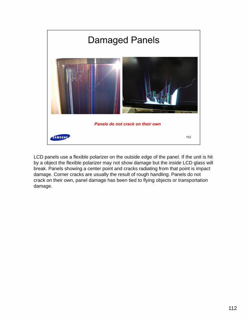
LCD panels use a flexible polarizer on the outside edge of the panel. If the unit is hit by a object the flexible polarizer may not show damage but the inside LCD glass will break. Panels showing a center point and cracks radiating from that point is impact damage. Corner cracks are usually the result of rough handling. Panels do not crack on their own, panel damage has been tied to flying objects or transportation damage.
112

113
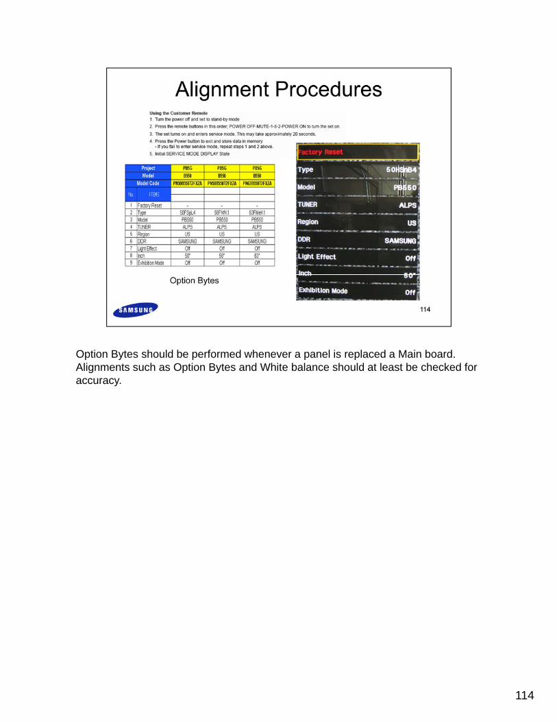
Option Bytes should be performed whenever a panel is replaced a Main board. Alignments such as Option Bytes and White balance should at least be checked for accuracy.
114
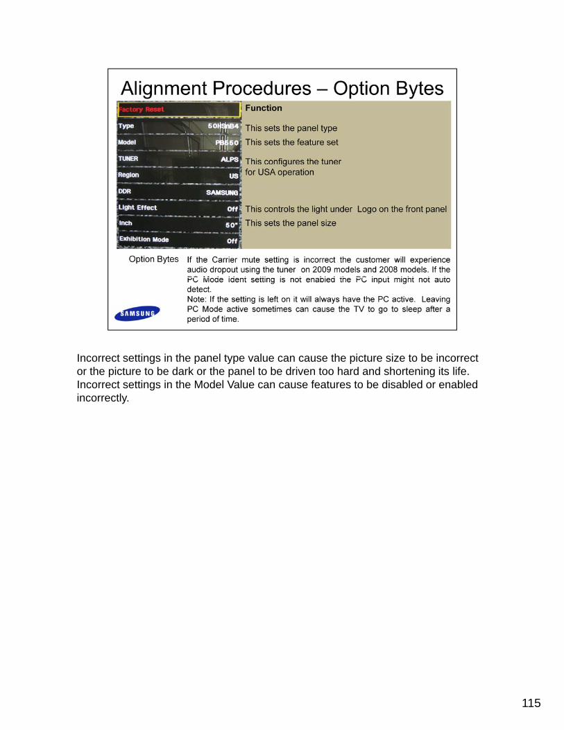
Incorrect settings in the panel type value can cause the picture size to be incorrect or the picture to be dark or the panel to be driven too hard and shortening its life. Incorrect settings in the Model Value can cause features to be disabled or enabled incorrectly.
115

116

The concept of 3D incorporates a phenomenon called persistence of vision where the human eye is tricked into seeing a flat image that appears to have depth to it. By using the space of the left and right eye and by flickering the picture at a high frequency, the effect is a perception of depth.
117
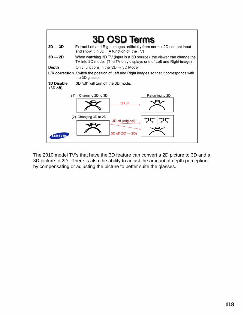
The 2010 model TV’s that have the 3D feature can convert a 2D picture to 3D and a 3D picture to 2D. There is also the ability to adjust the amount of depth perception by compensating or adjusting the picture to better suite the glasses.
118118

The 3D circuits can be tested by viewing the picture without the glasses and varying the depth control. It should vary between a picture that looks almost normal to one that looks like it has a shadow or a double image.
119

Please see the S/M for details
120

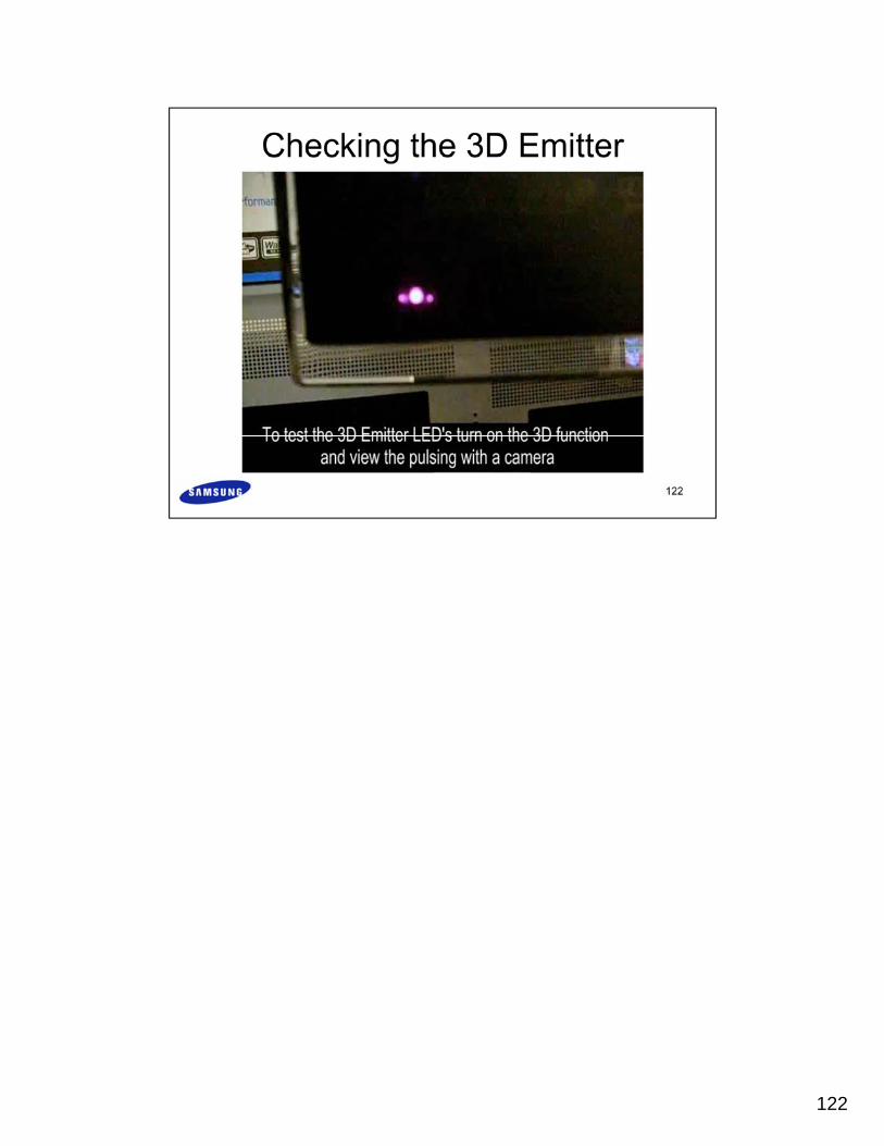
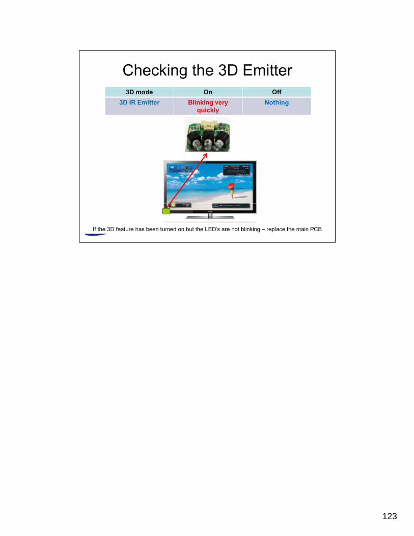
Another test of the 3D system is the IR Emitter LED function test. If the LED’s are not flashing with the 3D turned on , the LED’s and/or Main PCB must be replaced.
121
122
123
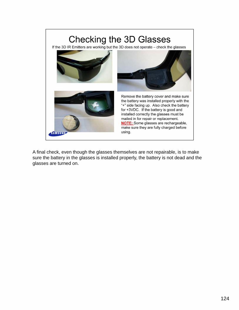
A final check, even though the glasses themselves are not repairable, is to make sure the battery in the glasses is installed properly, the battery is not dead and the glasses are turned on.
124
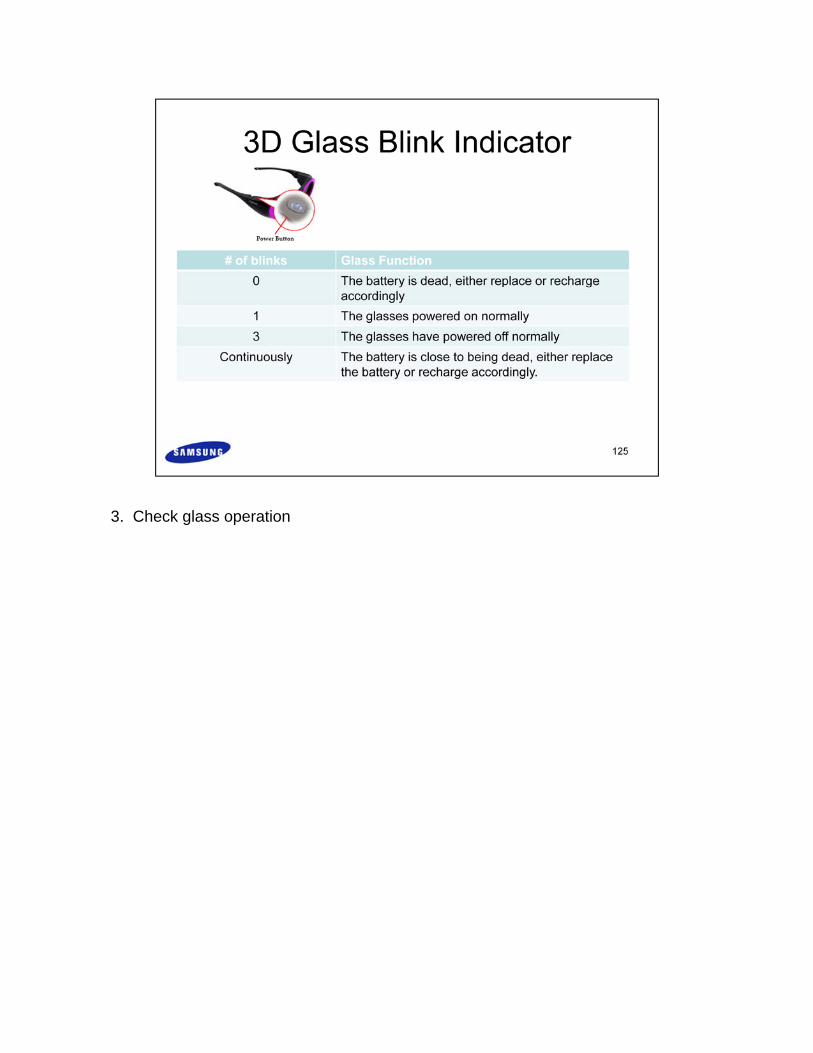
3. Check glass operation

126