Embed Size (px)
Citation preview
CESDig & CEletro 2018/19 / Elect. Fundamentals Floyd & Buchla © Pearson Education. © Trustees of Boston U niversityJFCircuitos Elétricos e Sistemas Digitais
2018-2019 - 1.º Semestre
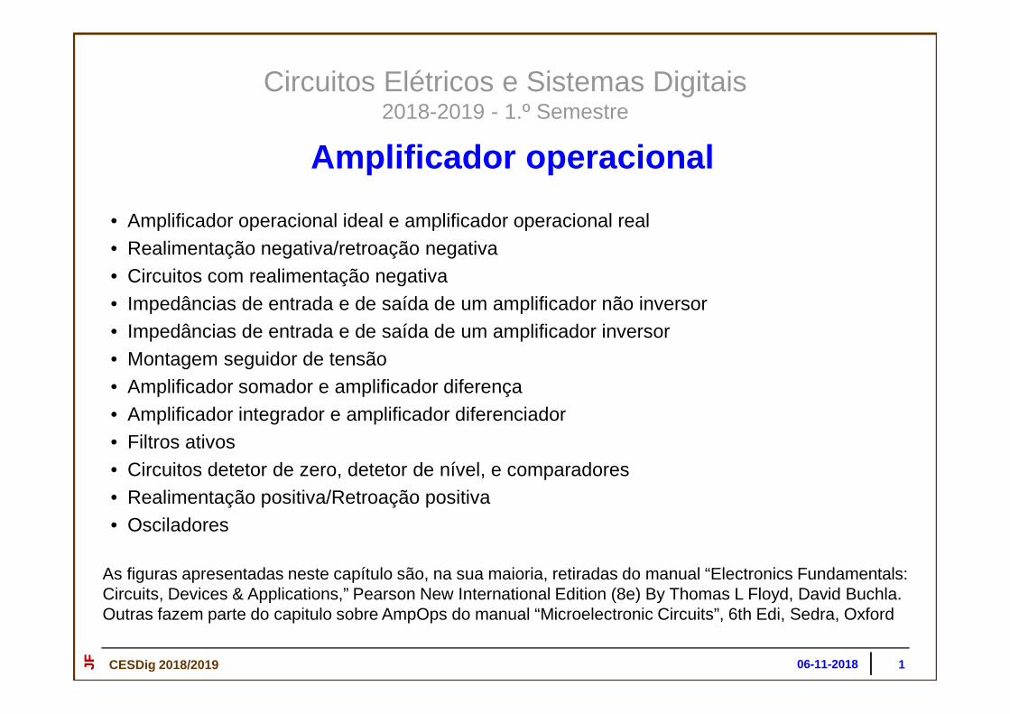
Amplificador operacional
• Amplificador operacional ideal e amplificador operacional real• Realimentação negativa/retroação negativa • Circuitos com realimentação negativa • Impedâncias de entrada e de saída de um amplificador não inversor• Impedâncias de entrada e de saída de um amplificador inversor• Montagem seguidor de tensão • Amplificador somador e amplificador diferença • Amplificador integrador e amplificador diferenciador• Filtros ativos• Circuitos detetor de zero, detetor de nível, e comparadores• Realimentação positiva/Retroação positiva • Osciladores
1CESDig 2018/2019 30-10-2018JF 06-11-2018
As figuras apresentadas neste capítulo são, na sua maioria, retiradas do manual “Electronics Fundamentals:Circuits, Devices & Applications,” Pearson New International Edition (8e) By Thomas L Floyd, David Buchla. Outras fazem parte do capitulo sobre AmpOps do manual “Microelectronic Circuits”, 6th Edi, Sedra, Oxford

CESDig & CEletro 2018/19 / Elect. Fundamentals Floyd & Buchla © Pearson Education. © Trustees of Boston U niversityJFSímbolos do amplificador operacional
e tipos de empacotamento
Fonte de alimentação positiva
Fonte de alimentação positiva
2
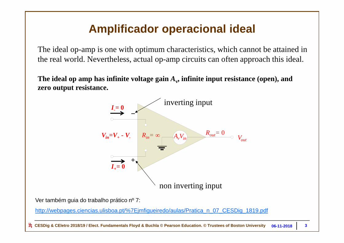
CESDig & CEletro 2018/19 / Elect. Fundamentals Floyd & Buchla © Pearson Education. © Trustees of Boston U niversityJFAmplificador operacional ideal
3
The ideal op-amp is one with optimum characteristics, which cannot be attained in the real world. Nevertheless, actual op-amp circuits can often approach this ideal.
The ideal op amp has infinite voltage gain Av, infinite input resistance (open), and zero output resistance.
Vin=V+ - V- Rin= ∞ AvVin Vout
Rout= 0
+
−
06-11-2018
Ver também guia do trabalho prático nº 7:
http://webpages.ciencias.ulisboa.pt/%7Ejmfigueiredo/aulas/Pratica_n_07_CESDig_1819.pdf
I-= 0
I+= 0
inverting input
non inverting input

CESDig & CEletro 2018/19 / Elect. Fundamentals Floyd & Buchla © Pearson Education. © Trustees of Boston U niversityJFAmplificador operacional real
4
Practical op-amps have limitations including power and voltage limits. A practical op-amp has high voltage gain Av, high input resistance, and low output resistance.
VinRin AvVin VoutRout
There are two inputs, labeled inverting and non inverting because of the phase relation of the input and output signals.
+
−
inverting input
non inverting input
06-11-2018
Ver também guia do trabalho prático nº 7:
http://webpages.ciencias.ulisboa.pt/%7Ejmfigueiredo/aulas/Pratica_n_07_CESDig_1819.pdf
I-≅ 0
I+ ≅ 0
Vin=V+ - V-
+VCC ( 15 V)
Vin=V+ - V-(µV)
Vout
+VCC
-VCC-VCC ( -15 V)
Av >> 1

CESDig & CEletro 2018/19 / Elect. Fundamentals Floyd & Buchla © Pearson Education. © Trustees of Boston U niversityJFUm amplificador operacional tem um ganho em
malha aberta muito elevadoWithout negative feedback, an extremely small difference in the two input voltagesdrives the op-amp to its output limits and it becomes nonlinear.
Terminal de entrada não inversora
Terminal de entrada inversora
Terminal de entrada não inversora
5
CESDig & CEletro 2018/19 / Elect. Fundamentals Floyd & Buchla © Pearson Education. © Trustees of Boston U niversityJF
Montagens com realimentação/retroação(feedback)
6

CESDig & CEletro 2018/19 / Elect. Fundamentals Floyd & Buchla © Pearson Education. © Trustees of Boston U niversityJF
A realimentação num amplificador consiste em reintroduzir uma parte do sinal de saída na entrada. Dependendo da(s) malha(s) exterior(es), a realimentação pode reforçar o sinal de entrada, ou contrariá-lo. Assim, a realimentação positiva correspondente a um reforço do sinal de entrada pela saída, e realimentação negativa, ao caso oposto.
Av
Feedback circuit
7
Realimentação – Retroação(feedback)
B
Acl = AvB
Av+vin vout
= +
=
1 −
= ≡
Av =ganho em malha aberta/sem realimentação
Acl,f = ganho em malha fechada/com realimentação
B = factor de realimentação
Av+vin vout
CESDig & CEletro 2018/19 / Elect. Fundamentals Floyd & Buchla © Pearson Education. © Trustees of Boston U niversityJF
Montagem não inversora com realimentação/retroação negativa
8

CESDig & CEletro 2018/19 / Elect. Fundamentals Floyd & Buchla © Pearson Education. © Trustees of Boston U niversityJFAmp -ops com realimentação/retroação negativa
(feedback negativo)
= − = −
=
= ≡
se >>1, ==
The op-amp has a differential amplifier
as the input stage. When a feedback
network returns a fraction B of the output
Vout, Vf =B Vout, to the inverting input,
only the difference signal (Vin – Vf) is
amplified.
9
B = factor de realimentação ou feedback

CESDig & CEletro 2018/19 / Elect. Fundamentals Floyd & Buchla © Pearson Education. © Trustees of Boston U niversityJFRealimentação negativa/Retroação negativa
10
Negative feedback
In 1921, Harold S. Black was working on the problem of linearizing and stabilizing amplifiers. While traveling to work on the ferry, he suddenly realized that if he returned some of the output back to the input in opposite phase, he had a means of canceling distortion. One of the most important ideas in electronics was sketched out on his newspaper that morning.
+ Vout
Vin
V f −
Feedbacknetwork
The op-amp has a differential amplifier as the input stage. When a feedback network returns a fraction of the output to the inverting input , only the difference signal (Vin – Vf) is amplified.
06-11-2018
Ver também guia do trabalho prático nº 7:
http://webpages.ciencias.ulisboa.pt/%7Ejmfigueiredo/aulas/Pratica_n_07_CESDig_1819.pdf
Ri
Rf
I+≅ 0
I- ≅ 0

CESDig & CEletro 2018/19 / Elect. Fundamentals Floyd & Buchla © Pearson Education. © Trustees of Boston U niversityJFMontagem não inversora com
realimentação/retroação negativa
1
1
≅
1
11

CESDig & CEletro 2018/19 / Elect. Fundamentals Floyd & Buchla © Pearson Education. © Trustees of Boston U niversityJFMontagem não inversora com
realimentação/retroação negativa
12
Op amp circuits with negative feedback
Negative feedback is used in almost all linear op-amp circuits because it stabilizes the gain and reduces distortion. It can also increase the input resistance.
−
+
Feedback network
Vf
Vin
Rf
Ri
Vout
A basic configuration is a noninverting amplifier. The difference between Vin and Vf is very small due to feedback. Therefore, .in fV V≅
(NI) 1 fcl
i
RA
R= +
The closed-loop gain for the noninverting amplifier can be derived from this idea; it is controlled by the feedback resistors:
06-11-2018
Curto-circuito virtual entre as entradas do AmpOp

CESDig & CEletro 2018/19 / Elect. Fundamentals Floyd & Buchla © Pearson Education. © Trustees of Boston U niversityJFImpedância de entrada de um amplificador não invers or
13
Input resistance for the noninverting amplifier
The input resistance of an op-amp without feedback is Rin. For the 741C, the
manufacturer’s specified value of Rin is 2 MΩ.
Negative feedback increases this to Rin(NI) = (1 + AolB)Rin, Aol=Av. This is so large that for
all practical circuits it can be considered to be infinite.
Keep in mind that, although Rin(NI) is
extremely large, the op-amp is a dc amplifier
and still requires a dc bias path for the input.
−
+Vin
Rf
Ri
Vout
06-11-2018
>>1

CESDig & CEletro 2018/19 / Elect. Fundamentals Floyd & Buchla © Pearson Education. © Trustees of Boston U niversityJFImpedância de saída de um amplificador não inversor
14
Output resistance for the noninverting amplifier
The output resistance of an op-amp without feedback is Rout. Negative feedback decreases this by a factor of (1 + AolB). This is so small that for all practical circuits it can be considered to be zero.
(NI) 1out
outol
RR
A B=
+−
+Vin
Rf
Ri
Vout
The low output resistance implies that the output voltage is independent of the load resistance (as long as the current limit is not exceeded).
06-11-2018
>>1
Although Rout(I) is very small, this does not imply that an op-amp can drive any load. The maximum current that the op-amp can supply is limited. For the 741C, it is typically 20 mA.

CESDig & CEletro 2018/19 / Elect. Fundamentals Floyd & Buchla © Pearson Education. © Trustees of Boston U niversityJFImpedância de entrada e de saída de um
amplificador não inversor
15
( ) ( )( )( )in(NI) 1 1+ 100,000 0.040 2 M = ol inR A B R= + = Ω
The gain is
(I)
36 k1 1
1.5 kf
cli
RA
R
Ω= + = + =Ω
25
The input resistance is
8 GΩ
The feedback fraction is 10.040
25B = =
−
+Vin
Rf
Ri
Vout
36 kΩ
1.5 kΩ
What are the input and output resistances and the gain of the noninverting amplifier? Assume the op amp hasAol = 100,000, Rin = 2 MΩ, and Rout = 75 Ω.
06-11-2018

CESDig & CEletro 2018/19 / Elect. Fundamentals Floyd & Buchla © Pearson Education. © Trustees of Boston U niversityJFImpedância de entrada e de saída de um
amplificador não inversor
16
The last result illustrates why it is rarely necessary to calculate an exact value for the input resistance of a noninverting amplifier.
For practical circuits, you can assume it is ideal.−
+Vin
Rf
Ri
Vout
36 kΩ
1.5 kΩThe output resistance is
( )( )(NI)
75 =
1 1+ 100,000 0.040out
outol
RR
A B
Ω= =+
0.019 Ω
This extremely small resistance is close to ideal. As in the case of the input resistance, it is rarely necessary to calculate an exact value for the noninverting amplifier.
06-11-2018
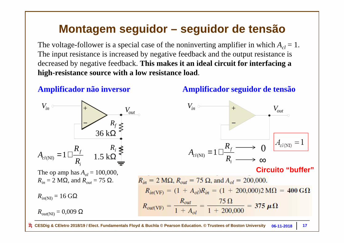
CESDig & CEletro 2018/19 / Elect. Fundamentals Floyd & Buchla © Pearson Education. © Trustees of Boston U niversityJFMontagem seguidor – seguidor de tensão
17
The voltage-follower is a special case of the noninverting amplifier in which Acl = 1. The input resistance is increased by negative feedback and the output resistance is decreased by negative feedback. This makes it an ideal circuit for interfacing a high-resistance source with a low resistance load.
−
+Vin Vout
06-11-2018
−
+Vin
Rf
Ri
Vout
36 kΩ
1.5 kΩ
Amplificador seguidor de tensão Amplificador não inversor
(NI) 1 fcl
i
RA
R= + (NI) 1 f
cli
RA
R= + 0
∞The op amp hasAol = 100,000, Rin = 2 MΩ, and Rout = 75 Ω.
Rin(NI) = 16 GΩ
Rout(NI) = 0,009 Ω
Circuito “buffer”

CESDig & CEletro 2018/19 / Elect. Fundamentals Floyd & Buchla © Pearson Education. © Trustees of Boston U niversityJF
Montagem inversora com realimentação/retroação negativa
18

CESDig & CEletro 2018/19 / Elect. Fundamentals Floyd & Buchla © Pearson Education. © Trustees of Boston U niversityJFMontagem inversora com
realimentação/retroação negativa
19
Op amp circuits with negative feedbackThe inverting amplifier is a basic configuration in which the noninverting input is grounded (sometimes through a resistor to balance the bias inputs). Again, the difference between Vin and Vf
is very small due to feedback; this implies that the inverting input is nearly at ground. This is referred to as a virtual ground. The virtual ground looks like ground to voltage, but not to current!
(I)f
cli
RA
R= −
The closed-loop gain for the inverting amplifier can be derived from this idea; again it is controlled by the feedback resistors ( ≫ ):
−
+
Vin
Rf
Ri
Vout
Virtual ground
06-11-2018
Ver também guia do trabalho prático nº 7:
http://webpages.ciencias.ulisboa.pt/%7Ejmfigueiredo/aulas/Pratica_n_07_CESDig_1819.pdf
! ! "!#$%
≈ >>1
if= i1
i1=Vin/Ri
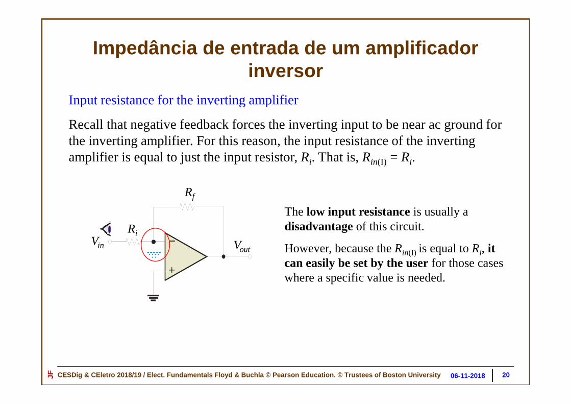
CESDig & CEletro 2018/19 / Elect. Fundamentals Floyd & Buchla © Pearson Education. © Trustees of Boston U niversityJFImpedância de entrada de um amplificador
inversor
20
Input resistance for the inverting amplifier
Recall that negative feedback forces the inverting input to be near ac ground for the inverting amplifier. For this reason, the input resistance of the inverting amplifier is equal to just the input resistor, Ri. That is, Rin(I) = Ri.
The low input resistance is usually a disadvantageof this circuit.
However, because theRin(I) is equal to Ri, it can easily be set by the userfor those cases where a specific value is needed.
−
+
Vin
Rf
Ri
Vout
06-11-2018

CESDig & CEletro 2018/19 / Elect. Fundamentals Floyd & Buchla © Pearson Education. © Trustees of Boston U niversityJFImpedância de saída de um amplificador
inversor
21
Output resistance for the inverting amplifier
The equation for the output resistance of the inverting amplifier is the essentially the same as the noninverting amplifier:
−
+
Vin
Rf
Ri
Vout
(I) 1out
outol
RR
A B=
+
Although Rout(I) is very small, this does not imply that an op-amp can drive any load.
The maximum current that the op-amp can supply is limited.
For the 741C, it is typically 20 mA.
06-11-2018

CESDig & CEletro 2018/19 / Elect. Fundamentals Floyd & Buchla © Pearson Education. © Trustees of Boston U niversityJFImpedância de entrada e de saída de um
amplificador inversor
22
−
+
Vin
Rf
Ri
Vout
The gain is (I)
36 k
1.5 kf
cli
RA
R
Ω= − = − =Ω 36 kΩ
1.5 kΩ
−24
The input resistance = Ri = 1.5 kΩ
The output resistance is nearly identical to the noninverting case, where it was shown to be negligible.
What is the input resistance and the gain of the inverting amplifier?
06-11-2018
Outro exemplo: Ri = 1 kΩ e Rf = 100 kΩ.

CESDig & CEletro 2018/19 / Elect. Fundamentals Floyd & Buchla © Pearson Education. © Trustees of Boston U niversityJF
Circuitos aritméticos
Montagens somadoras
2313-11-2018

CESDig & CEletro 2018/19 / Elect. Fundamentals Floyd & Buchla © Pearson Education. © Trustees of Boston U niversityJFAmplificador somador
24
There are a number of useful applications for the basic inverting amplifier configuration. One is the summing amplifier that uses two or more inputs and one output.
13-11-2018

CESDig & CEletro 2018/19 / Elect. Fundamentals Floyd & Buchla © Pearson Education. © Trustees of Boston U niversityJF
Summing amplifier
There are a number of useful applications for the basic inverting amplifier configuration. One is the summing amplifier that uses two or more inputs and one output.
R1VIN1
VIN2
VIN3
VINn
R2
R3
Rn
Rf
+
−VOUT
The virtual ground isolates the inputs from each other. Input current from each input is passed to Rf, which develops an output voltage that is proportional to the algebraic sum of the inputs.
Virtual ground
Amplificador somador
2513-11-2018

CESDig & CEletro 2018/19 / Elect. Fundamentals Floyd & Buchla © Pearson Education. © Trustees of Boston U niversityJF
Averaging amplifier
An averaging amplifier is a variation of the summing amplifier in which all input resistors are equal. The feedback resistor is the reciprocal of the number of inputs times the input resistor value.
R1VIN1
VIN2
VIN3
R2
R3
Rf
+
−VOUT
For example, if there are three input resistors, each with a value of 10 kΩ, then Rf = 3.3 kΩ to form an averaging amplifier.
10 kΩ
10 kΩ
10 kΩ
3.3 kΩ
Amplificador somador
2613-11-2018

CESDig & CEletro 2018/19 / Elect. Fundamentals Floyd & Buchla © Pearson Education. © Trustees of Boston U niversityJF
Scaling adder
A scaling adder is another variation of the summing amplifier in which the input resistors are adjusted to weight inputs differently. The input “weight” is proportional to the current from that input.
R1VIN1
VIN2
VIN3
R2
R3
Rf
+
−VOUT
Larger resistors will allow less current for a given input voltage, so they have less “weight” than smaller resistors. In the case shown, VIN3 is “weighted” 2 times more than VIN2, which is 2 times more than VIN1.
10 kΩ
5.0 kΩ
2.5 kΩ
10 kΩ
Amplificador somador
2713-11-2018

CESDig & CEletro 2018/19 / Elect. Fundamentals Floyd & Buchla © Pearson Education. © Trustees of Boston U niversityJF
Scaling adder
R1VIN1
VIN2
VIN3
R2
R3
Rf
+
−VOUT
10 kΩ
5.0 kΩ
2.5 kΩ
10 kΩ
What is VOUT for the scaling adder if all inputs are + 1.0 V?
By Ohm’s law, the currents into Rf are I1 = 0.1 mA, I2 = 0.2 mA and I3 = 0.4 mA.
Using the superposition theorem, the current in Rf is 0.7 mA. From Ohm’s law, VOUT = 7 V
Amplificador somador
Ver também guia do trabalho prático nº 7:
http://webpages.ciencias.ulisboa.pt/%7Ejmfigueiredo/aulas/Pratica_n_07_CESDig_1819.pdf
2813-11-2018

CESDig & CEletro 2018/19 / Elect. Fundamentals Floyd & Buchla © Pearson Education. © Trustees of Boston U niversityJF
Montagem diferença(subtração )
2913-11-2018

CESDig & CEletro 2018/19 / Elect. Fundamentals Floyd & Buchla © Pearson Education. © Trustees of Boston U niversityJF
Este circuito é semelhante ao somador e é usado para subtrair dois sinais VIN1 e VIN2. O terminal v+ tem uma tensão imposta pelo divisor resistivo R3 e R4. A tensão no terminal v-
é igual à tensão em v+ desde que o AmpOp não esteja na zona de saturação.
Curto-circuito virtual
Amplificador diferença
30
VOUT
R2
+
−VIN1
VIN2
R1
R3 R4
' () (
* '* * '
VOUT
R
+
−VIN1
VIN2
R
R R
' '* '
(para a dedução das expressões abaixo pode-se, por exemplo, aplicar o princípio da sobreposição.)
13-11-2018

CESDig & CEletro 2018/19 / Elect. Fundamentals Floyd & Buchla © Pearson Education. © Trustees of Boston U niversityJF
Montagem integradora
3113-11-2018

CESDig & CEletro 2018/19 / Elect. Fundamentals Floyd & Buchla © Pearson Education. © Trustees of Boston U niversityJFAn ideal op -amp integrator.
32
FIGURE 19–12
13-11-2018
+ 1, - .
!/+

CESDig & CEletro 2018/19 / Elect. Fundamentals Floyd & Buchla © Pearson Education. © Trustees of Boston U niversityJF
IntegratorsFor the ideal integrator, the rate of change of the output is given by
R
C
VinVout
out in
i
V V
t R C
∆ = −∆
The minus sign in the equation is due to the inverting amplifier. If the input is a square wave centered about 0 V, the output is a negative triangular wave (provided saturation is not reached).
Vin
Vout
0 V
0 V+
−
Amplificador integrador
3313-11-2018
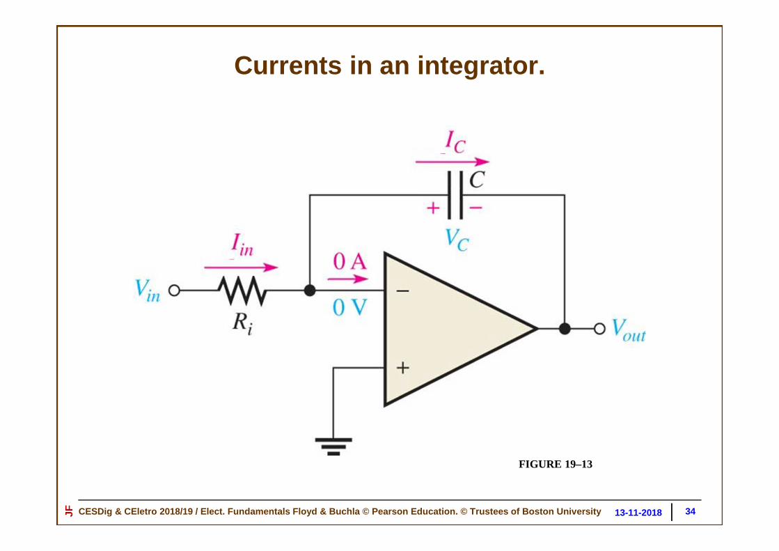
CESDig & CEletro 2018/19 / Elect. Fundamentals Floyd & Buchla © Pearson Education. © Trustees of Boston U niversityJFCurrents in an integrator.
34
FIGURE 19–13
13-11-2018

CESDig & CEletro 2018/19 / Elect. Fundamentals Floyd & Buchla © Pearson Education. © Trustees of Boston U niversityJFA constant input voltage produces a ramp on
the output.
35
FIGURE 19–15
13-11-2018

CESDig & CEletro 2018/19 / Elect. Fundamentals Floyd & Buchla © Pearson Education. © Trustees of Boston U niversityJF
Integrators
Mathematical integration is basically a summing process. Within certain limitations, an integrator circuit simulates this process.
The ideal integrator is essentially a summing amplifier with a capacitor in place of the feedback resistor.
R
C
Vin
Vout
In practical circuits, a large value resistor is usually in parallel with the capacitor to prevent the output from drifting into saturation.
Rf
+
−
Amplificador integrador prático
Ver também guia do trabalho prático nº 7:
http://webpages.ciencias.ulisboa.pt/%7Ejmfigueiredo/aulas/Pratica_n_07_CESDig_1819.pdf
3613-11-2018

CESDig & CEletro 2018/19 / Elect. Fundamentals Floyd & Buchla © Pearson Education. © Trustees of Boston U niversityJFAmplificador integrador
37
FIGURE 19–16
13-11-2018

CESDig & CEletro 2018/19 / Elect. Fundamentals Floyd & Buchla © Pearson Education. © Trustees of Boston U niversityJF
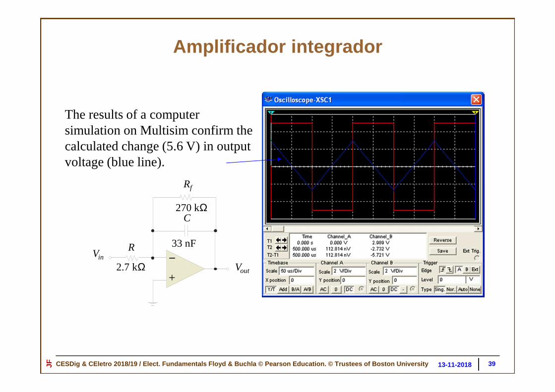
R
C
Vin
Vout
( ) ( )5 V
100 µs =2.7 k 33 nF
inout
i
VV t
R C∆ = − ∆ = −
Ω
A 5 kHz square wave with 10 Vpp is applied to a practical integrator. Show the output waveform voltages.
33 nF
2.7 kΩ
270 kΩ
Rf
During the positive input (½ the period), the change in the output is
5.6 V
The feedback resistor (Rf) is large compared to R, so has little effect on the shape of the waveform. In a practical circuit, it will cause the output waveform to center on zero as shown on the following slide.+
−
Amplificador integrador
3813-11-2018
CESDig & CEletro 2018/19 / Elect. Fundamentals Floyd & Buchla © Pearson Education. © Trustees of Boston U niversityJF
R
C
Vin
Vout
33 nF
2.7 kΩ
270 kΩ
Rf
The results of a computer simulation on Multisim confirm the calculated change (5.6 V) in output voltage (blue line).
+
−
Amplificador integrador
3913-11-2018

CESDig & CEletro 2018/19 / Elect. Fundamentals Floyd & Buchla © Pearson Education. © Trustees of Boston U niversityJF
Montagem diferenciadora
4013-11-2018

CESDig & CEletro 2018/19 / Elect. Fundamentals Floyd & Buchla © Pearson Education. © Trustees of Boston U niversityJFAn ideal op -amp differentiator.
41
FIGURE 19–17
13-11-2018
. + , d'+d+

CESDig & CEletro 2018/19 / Elect. Fundamentals Floyd & Buchla © Pearson Education. © Trustees of Boston U niversityJF
Differentiators
The output voltage for the ideal differentiator is given by
+
−
Rf
CVinVout
Cout f
VV R C
t = −
The minus sign in the equation is due to the inverting amplifier. If the input is a ramp, the output is a negative dc level for the positive slope and a positive dc level for the negative slope.
Vin
Vout
Amplificador diferenciador
4213-11-2018

CESDig & CEletro 2018/19 / Elect. Fundamentals Floyd & Buchla © Pearson Education. © Trustees of Boston U niversityJFA differentiator with a ramp input.
43
FIGURE 19–18
13-11-2018
. + , d'+d+

CESDig & CEletro 2018/19 / Elect. Fundamentals Floyd & Buchla © Pearson Education. © Trustees of Boston U niversityJFOutput of a differentiator with a series of
positive and negative ramps (triangle wave) on the input.
44
FIGURE 19–19
13-11-2018
. + , d'+d+
CESDig & CEletro 2018/19 / Elect. Fundamentals Floyd & Buchla © Pearson Education. © Trustees of Boston U niversityJF
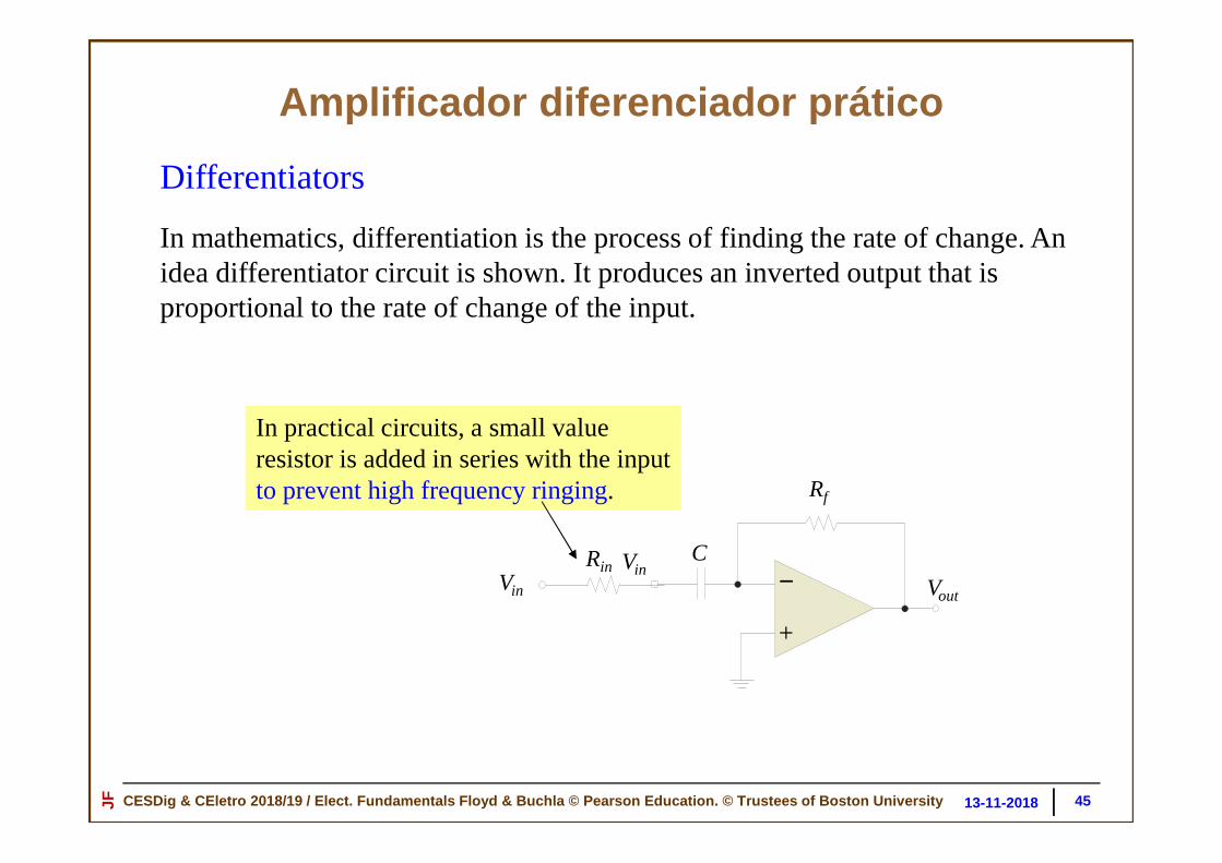
Differentiators
In mathematics, differentiation is the process of finding the rate of change. An idea differentiator circuit is shown. It produces an inverted output that is proportional to the rate of change of the input.
+
−CVin
Vout
In practical circuits, a small value resistor is added in series with the input to prevent high frequency ringing.
RinVin
Rf
Amplificador diferenciador prático
4513-11-2018
CESDig & CEletro 2018/19 / Elect. Fundamentals Floyd & Buchla © Pearson Education. © Trustees of Boston U niversityJFOutput of a differentiator with a series of
positive and negative ramps (triangle wave) on the input
46
FIGURE 19–20
13-11-2018
. + , d'+d+

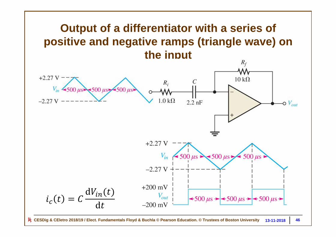
CESDig & CEletro 2018/19 / Elect. Fundamentals Floyd & Buchla © Pearson Education. © Trustees of Boston U niversityJF
A 1.0 kHz, 10 Vpp triangular wave is applied to a practical differentiator as shown. Show the output in relationship to the input.
When the input has a positive slope, the output is
( )( )10 V2.7 k 100 nF
0.5 msC
out f
VV R C
t = − = − Ω =
Rf
CVin
100 nF
2.7 kΩ
120 Ω+
− Vout
Rin
Vin
+5.0 V
−5.0 V
0 V
−5.4 V
By symmetry, when the input has a negative slope, the output will be +5.4 V.
0 1 ms 2 ms
Amplificador diferenciador
4713-11-2018

CESDig & CEletro 2018/19 / Elect. Fundamentals Floyd & Buchla © Pearson Education. © Trustees of Boston U niversityJF
The results of a computer simulation on Multisim confirm the calculated output voltages (±5.4 V). The output voltage is the blue line.
Amplificador diferenciador
48
Rf
CVin
100 nF
2.7 kΩ
120 Ω+
− Vout
Rin
13-11-2018
CESDig & CEletro 2018/19 / Elect. Fundamentals Floyd & Buchla © Pearson Education. © Trustees of Boston U niversityJF 49
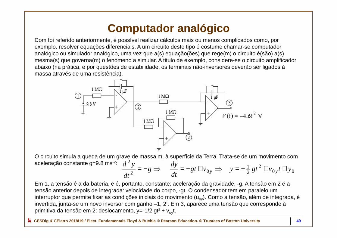
Computador analógicoCom foi referido anteriormente, é possível realizar cálculos mais ou menos complicados como, por exemplo, resolver equações diferenciais. A um circuito deste tipo é costume chamar-se computador analógico ou simulador analógico, uma vez que a(s) equação(ões) que rege(m) o circuito é(são) a(s) mesma(s) que governa(m) o fenómeno a simular. A titulo de exemplo, considere-se o circuito amplificador abaixo (na prática, e por questões de estabilidade, os terminais não-inversores deverão ser ligados à massa através de uma resistência).
O circuito simula a queda de um grave de massa m, à superfície da Terra. Trata-se de um movimento com aceleração constante g=9.8 ms-2:
002
21
02
2
ytvgtyvgtdt
dyg
dt
ydyy ++−=⇒+−=⇒−=
Em 1, a tensão é a da bateria, e é, portanto, constante: aceleração da gravidade, -g. A tensão em 2 é a tensão anterior depois de integrada: velocidade do corpo, -gt. O condensador tem em paralelo um interruptor que permite fixar as condições iniciais do movimento (uoy). Como a tensão, além de integrada, é invertida, junta-se um novo inversor com ganho –1, 2’. Em 3, aparece uma tensão que corresponde à primitiva da tensão em 2: deslocamento, y=-1/2 gt2 + voyt.
CESDig & CEletro 2018/19 / Elect. Fundamentals Floyd & Buchla © Pearson Education. © Trustees of Boston U niversityJF
Filtros ativos de 1.ª ordem
5013-11-2018
Ver também Guia P08: Circuitos com AmOps – filtros ativos
http://webpages.ciencias.ulisboa.pt/%7Ejmfigueiredo/aulas/Pratica_n_08_CESDig_1819.pdf

CESDig & CEletro 2018/19 / Elect. Fundamentals Floyd & Buchla © Pearson Education. © Trustees of Boston U niversityJF
Integrators
R
C
Vin
Vout
Rf
+
−
Filtro passa-baixo
Ver também guia do trabalho prático nº 7:
http://webpages.ciencias.ulisboa.pt/%7Ejmfigueiredo/aulas/Pratica_n_07_CESDig_1819.pdf
5113-11-2018
A filter selects certain frequencies and excludes others. Active filters use op-amps to optimize the frequency response. A low-pass active filter and its response:
The gain for this filter is 1 (0 dB) for f < fc.

CESDig & CEletro 2018/19 / Elect. Fundamentals Floyd & Buchla © Pearson Education. © Trustees of Boston U niversityJF
+
−C
Vin Vout
Rin
Rf
Filtro passa-alto e efeito da largura de banda do A mpOP
5213-11-2018
Resposta em frequência.
By reversing the resistor and capacitor in the low-pass circuit, a high-pass active filter is created. This filter has a gain of 1 (0 dB) at frequencies where f > fc.

CESDig & CEletro 2018/19 / Elect. Fundamentals Floyd & Buchla © Pearson Education. © Trustees of Boston U niversityJFSingle-pole, low -pass active filter and response curve.Active filters use op-amps to optimize the frequency response. A low-pass active filter and its response.
FIGURE 19–33
5313-11-2018
The gain for this filter is 1 (0 dB) for f < fc.
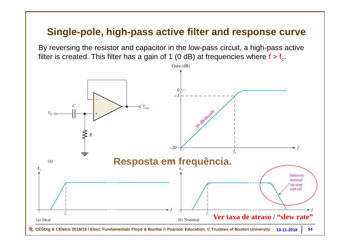
CESDig & CEletro 2018/19 / Elect. Fundamentals Floyd & Buchla © Pearson Education. © Trustees of Boston U niversityJFSingle-pole, high-pass active filter and response c urve
By reversing the resistor and capacitor in the low-pass circuit, a high-pass active filter is created. This filter has a gain of 1 (0 dB) at frequencies where f > fc.
FIGURE 19–37
5413-11-2018
Resposta em frequência.
Ver taxa de atraso / “slew rate”

CESDig & CEletro 2018/19 / Elect. Fundamentals Floyd & Buchla © Pearson Education. © Trustees of Boston U niversityJF
Definições gerais de largura de banda e
de frequência de corte
5520-11-2018

CESDig & CEletro 2018/19 / Elect. Fundamentals Floyd & Buchla © Pearson Education. © Trustees of Boston U niversityJFResposta em frequência e largura de banda
56
• Resposta em frequência de um sistema corresponde à análise do comportamento do sistemaquanto ao seu ganho numa certa faixa de frequências (ou frequência angular).
• A representação gráfica da resposta em frequência de uma rede elétrica traduz-se nos diagramas de Bode. A representação de Bode consiste em dois diagramas, um relativo ao ganho com uma escala linear no eixo das ordenadas (ganho em decibéis (dB) ou em volt por volt (V/V)), e o outro diagrama correspondendo à diferença de fase entre os sinais de entrada e de saída . A unidade mais utilizada para o ganho é o dB, mas pode ser usado o dBm, que corresponde ao nível de potência em dB em relação ao nível de referência de 1 mW). Em ambos no eixo das abscissas representa-se a frequência (Hz) ou frequência angular (rad/s) numa escala logarítmica.
• A largura de banda é um conceito central em diversos campos de conhecimento, incluindo teoria da informação, sistemas de comunicação rádio e óticos, processamento de sinais, eletrónica e espectroscopia. Em sistemas de comunicação a largura de banda corresponde à faixa de frequência ocupada pelo sinal modulado.
• Em eletrónica normalmente corresponde à faixa de fre quências na qual o sistema tem uma resposta em frequência aproximadamente plana (com v ariação igual ou inferior a 3 dB).
• Quando se refere a sinais analógicos, a largura de banda corresponde à faixa de frequência, medida em hertz, para a qual a transformada de Fourier do sinal é diferente de zero. Esta definição normalmente é relaxada considerando um ce rto limiar de amplitude, tipicamente 3 dB em relação ao pico.
• Para sistemas, aplicam-se basicamente os conceitos acima, mas considerando a função de transferência do sistema .
https://pt.wikipedia.org/wiki/Largura_de_banda
20-11-2018

CESDig & CEletro 2018/19 / Elect. Fundamentals Floyd & Buchla © Pearson Education. © Trustees of Boston U niversityJFFiltros: largura de banda e frequência de corte
• Filtro passa-banda:A largura de banda (LB ou simplesmente B) de um filtro passa-banda é a parte da resposta em frequência do filtro que está situada na faixa de 3 dB do valor de pico da resposta em frequência. Ou seja, num filtro passa-banda LBé a diferença entre f2 e f1: LB = f2 − f2.
57
• Num filtro passa-baixo a largura de banda corresponde ao valor da frequência de corte (fc): LB = fC.
• A frequência de corte (fc) ou frequência metade da potência (f3dB) é a frequência abaixo da qual ou acima da qual a potência na saída de um sistema (circuito eletrónico, linha de transmissão, filtro ou amplificador) é reduzida a metade do valor máximo (valor de pico) da potência na faixa de passagem.
20-11-2018
0 dB
Frequência central
f0

CESDig & CEletro 2018/19 / Elect. Fundamentals Floyd & Buchla © Pearson Education. © Trustees of Boston U niversityJF
Circuitos não lineares com AmpOpsRetificadores de Precisão e Amplificadores
Logarítmico e Exponencial
5820-11-2018

CESDig & CEletro 2018/19 / Elect. Fundamentals Floyd & Buchla © Pearson Education. © Trustees of Boston U niversityJFSuper-díodo
59
Paul Horowitz and Winfield Hill, The Art of Electronics. 2nd ed. Cambridge University Press, Cambridge, 1989 ISBN 0-521-37095-7.
Função de transferência
Função de transferênciaDíodo
Super-díodo
20-11-2018

CESDig & CEletro 2018/19 / Elect. Fundamentals Floyd & Buchla © Pearson Education. © Trustees of Boston U niversityJFRetificador de precisão
60
The precision rectifier , also known as a super diode , is a configuration obtained with an operational amplifier in order to have a circuitbehaving like an ideal diode and rectifier.[1] It is useful for high-precision signal processing.
When the input voltage is negative, there is a negative voltage on the diode, so it works like an open circuit, no current flows through the load, and the output voltage is zero. When the input is positive, itis amplified by the operational amplifier, which switches the diode on. Current flows through the loadand, because of the feedback, the output voltage is equal to the input voltage. The actual threshold of the super diode is very close to zero, but is not zero. It equals the actualthreshold of the diode, divided by the gain of the operational amplifier.
This basic configuration has a problem, so it is not commonly used. When the input becomes (evenslightly) negative, the operational amplifier runs open-loop, as there is no feedback signal through thediode. For a typical operational amplifier with high open-loop gain, the output saturates. If the input then becomes positive again, the op-amp has to get out of the saturated state before positive amplification can take place again. This change generates some ringing and takes some time, greatlyreducing the frequency response of the circuit.
Paul Horowitz and Winfield Hill, The Art of Electronics. 2nd ed. Cambridge University Press, Cambridge, 1989 ISBN 0-521-37095-7.
20-11-2018

CESDig & CEletro 2018/19 / Elect. Fundamentals Floyd & Buchla © Pearson Education. © Trustees of Boston U niversityJFRetificador de precisão – circuito melhorado
61
In this case, when the input is greater than zero, D1 is off, and D2 is on, so the output is zero because one side of R2 is connected to the virtual ground, and there is no current through it. When the input is less than zero, D1 is on, and D2 is off, so the output is like the input with an amplification of − R2 / R1. Its input–output relationship is the following:
This circuit has the benefit that the op-amp never goes into saturation, but its output must change by two diode voltage drops (about 1.4 V) each time the input signal crosses zero. Hence, the slew rate of the operational amplifier and its frequency response (gain–bandwidth product) will limit high-frequency performance, especially for low signal levels, although an error of less than 1% at 100 kHz is possible.
Similar circuitry can be used to create a precision full-wave rectifier circuit.
http://sound.whsites.net/appnotes/an001.htm
20-11-2018
CESDig & CEletro 2018/19 / Elect. Fundamentals Floyd & Buchla © Pearson Education. © Trustees of Boston U niversityJFRetificador de precisão de meia onda
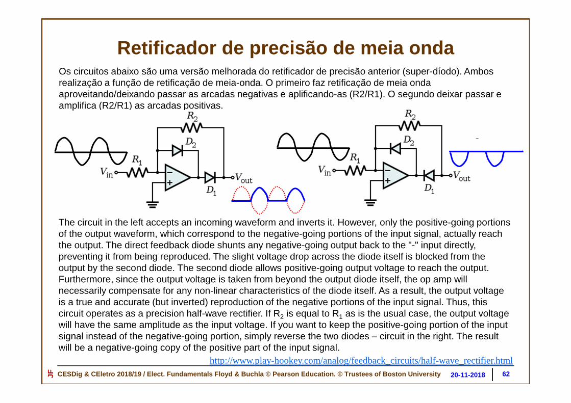
62
Os circuitos abaixo são uma versão melhorada do retificador de precisão anterior (super-díodo). Ambos realização a função de retificação de meia-onda. O primeiro faz retificação de meia ondaaproveitando/deixando passar as arcadas negativas e aplificando-as (R2/R1). O segundo deixar passar e amplifica (R2/R1) as arcadas positivas.
The circuit in the left accepts an incoming waveform and inverts it. However, only the positive-going portions of the output waveform, which correspond to the negative-going portions of the input signal, actually reach the output. The direct feedback diode shunts any negative-going output back to the "-" input directly, preventing it from being reproduced. The slight voltage drop across the diode itself is blocked from the output by the second diode. The second diode allows positive-going output voltage to reach the output. Furthermore, since the output voltage is taken from beyond the output diode itself, the op amp will necessarily compensate for any non-linear characteristics of the diode itself. As a result, the output voltage is a true and accurate (but inverted) reproduction of the negative portions of the input signal. Thus, this circuit operates as a precision half-wave rectifier. If R2 is equal to R1 as is the usual case, the output voltage will have the same amplitude as the input voltage. If you want to keep the positive-going portion of the input signal instead of the negative-going portion, simply reverse the two diodes – circuit in the right. The result will be a negative-going copy of the positive part of the input signal.
http://www.play-hookey.com/analog/feedback_circuits/half-wave_rectifier.html
20-11-2018

CESDig & CEletro 2018/19 / Elect. Fundamentals Floyd & Buchla © Pearson Education. © Trustees of Boston U niversityJFRetificador de precisão de meia onda
6320-11-2018
Para 5 0, 8 *
Para 9 0, 8 0D2 evita a saturação do AmpOp
Qual é a função realizada pelo circuito se invertermos os sentidos dos díodos?
CESDig & CEletro 2018/19 / Elect. Fundamentals Floyd & Buchla © Pearson Education. © Trustees of Boston U niversityJFQual é a função realizada por este circuito?
6420-11-2018
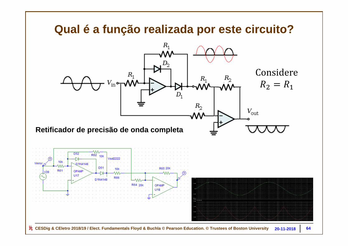
Retificador de precisão de onda completa
Considere
* =

CESDig & CEletro 2018/19 / Elect. Fundamentals Floyd & Buchla © Pearson Education. © Trustees of Boston U niversityJFRetificador de precisão de onda completa
65
The half-wave rectifier kept only those parts of the original input signal that were positive (or negative). Is there a way to keep both halves of the input signal, and yet render them both with the same output polarity? This is the behavior of a full-wave rectifier.
The circuit shown above (considere no que segue R1=10 kΩ e R2=20 kΩ) performs full-wave rectification on the input signal, as shown. If you wish the final output to be positive instead of negative, simply reverse the two diodes in the half-wave rectifier section.The full-wave rectifier depends on the fact that both the half-wave rectifier and the summing amplifier are precision circuits. It operates by producing an inverted half-wave-rectified signal and then adding that signal at double amplitude to the original signal in the summing amplifier. The result is a reversal of the selected polarity of the input signal.The resistor values shown are reasonable; the resistors themselves must be of high precision in order to keep the rectification process accurate. If for some reason you must build such a circuit with a different set of resistance values, you must maintain the indicated 2:1 resistance ratio, and you must still use precision resistors in order to obtain accurate results.
http://www.play-hookey.com/analog/feedback_circuits/full-wave_rectifier.html
20-11-2018

CESDig & CEletro 2018/19 / Elect. Fundamentals Floyd & Buchla © Pearson Education. © Trustees of Boston U niversityJFAmplificadores Logarítmico e exponencial
Sabe-se que na natureza e no dia-a-dia muitos fenómenos variam de forma logarítmica ou exponencial.
66
@ ' ; @B 'B @ , e'8 'B .Deonderesultaque@B 'B @I JKL/KN 1 ,obtendo-se'8 'Q ∙ ln '
∙ @I 1
IR
ID
R
V0
Vin
No amplificador logarítmico , a tensão de saída é o logarítmico da tensão de entrada:
Trocando de posição a resistência e o díodo obtém-se o amplificador exponencial :
@B 'B @ '8 , e'B ':Deonderesultaque,'8 ∙ @I J
K"KN 120-11-2018
CESDig & CEletro 2018/19 / Elect. Fundamentals Floyd & Buchla © Pearson Education. © Trustees of Boston U niversityJF
Circuitos não -lineares com AmpOps
6720-11-2018
CESDig & CEletro 2018/19 / Elect. Fundamentals Floyd & Buchla © Pearson Education. © Trustees of Boston U niversityJF 68
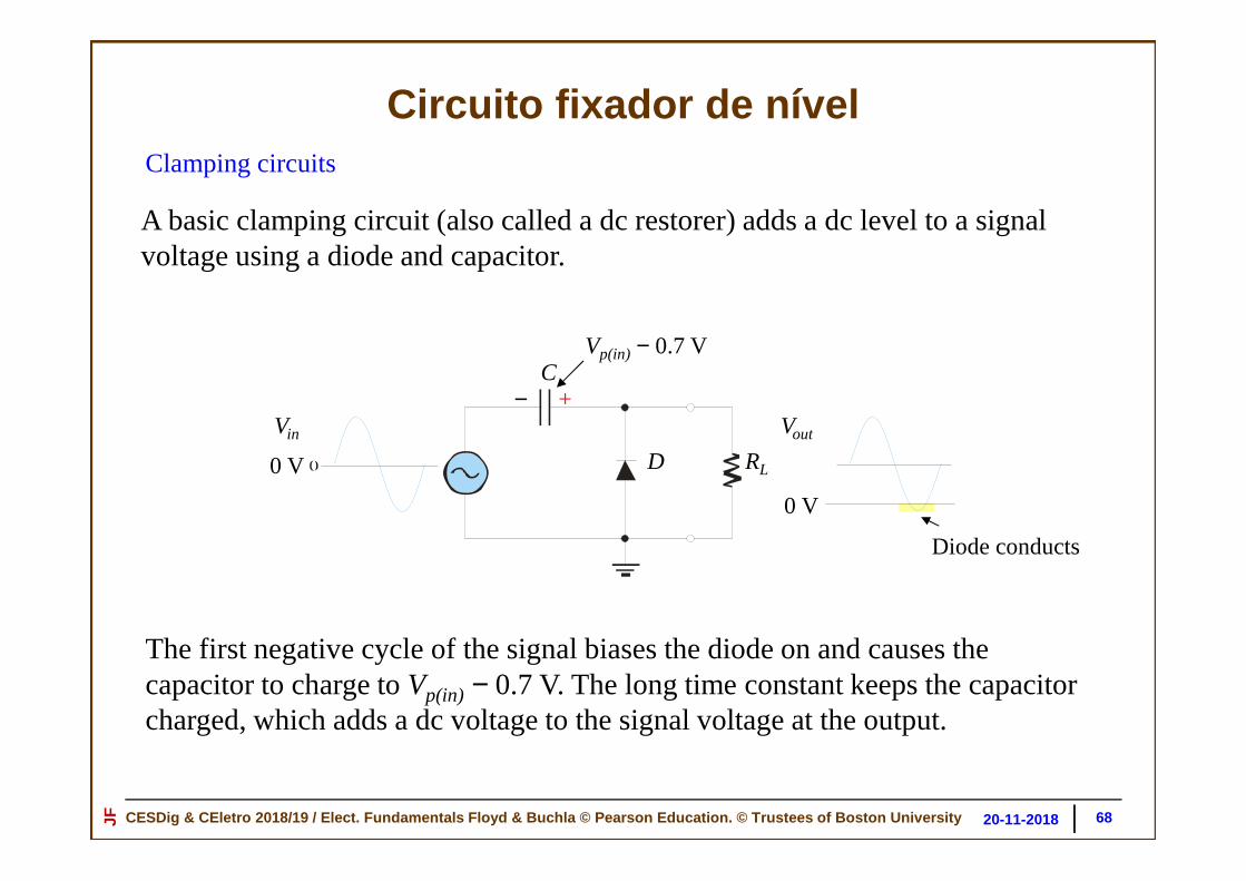
Circuito fixador de nívelClamping circuits
A basic clamping circuit (also called a dc restorer) adds a dc level to a signal voltage using a diode and capacitor.
The first negative cycle of the signal biases the diode on and causes the capacitor to charge to Vp(in) − 0.7 V. The long time constant keeps the capacitor charged, which adds a dc voltage to the signal voltage at the output.
Vp(in) − 0.7 V
Vin Vout
+
0 V
0 V
RL
−C
D
Diode conducts
20-11-2018

CESDig & CEletro 2018/19 / Elect. Fundamentals Floyd & Buchla © Pearson Education. © Trustees of Boston U niversityJF 69
Circuito fixador de nível com AmpOP
Clamping circuits
Active diode circuits use an op-amp and feedback to closely approximate the behavior of an ideal diode. The same clamping circuit with an active diode has a nearly ideal response.
The 0.7 V diode drop in the basic circuit can be a problem for low-level signals, which are common in signal processing applications.
RL
R1
C+−Vin Vout
D
Vin
0 V
0 V
+
−
20-11-2018
CESDig & CEletro 2018/19 / Elect. Fundamentals Floyd & Buchla © Pearson Education. © Trustees of Boston U niversityJF 70
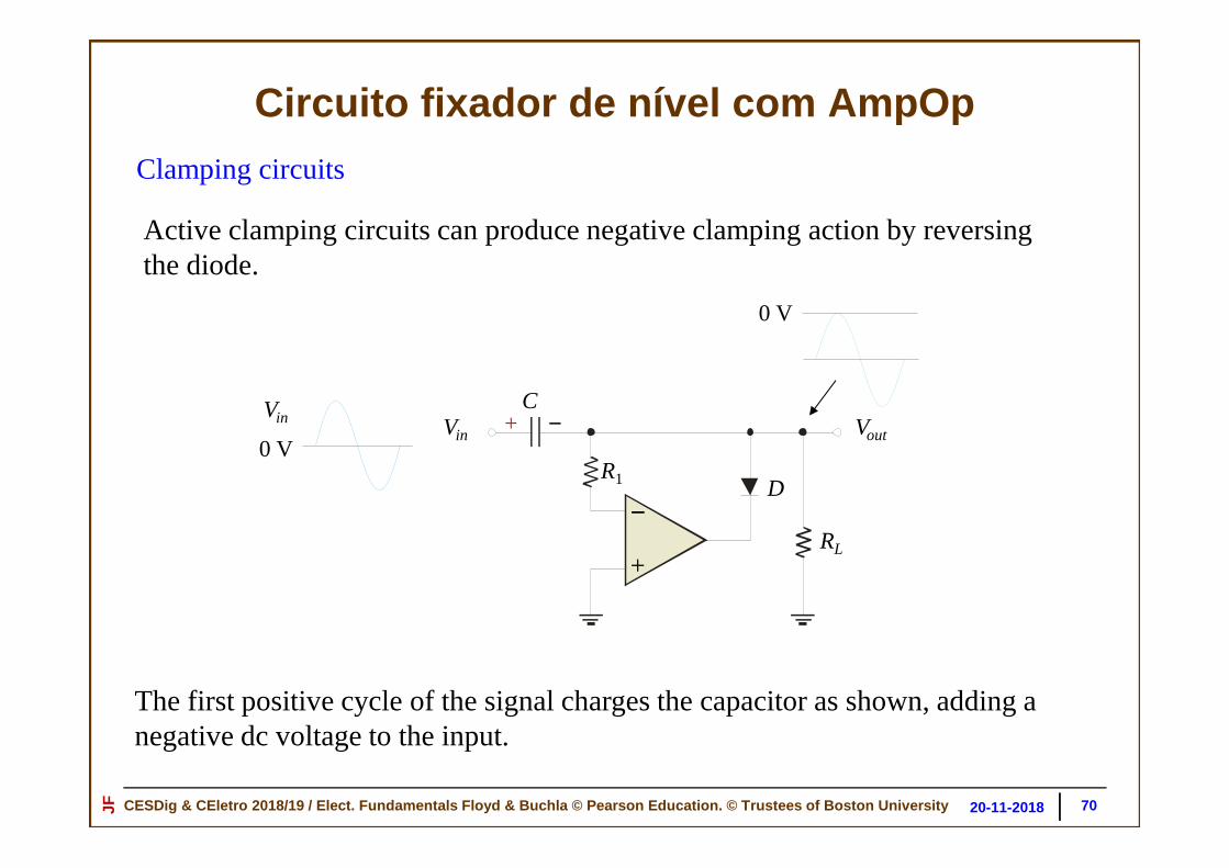
Circuito fixador de nível com AmpOp
Clamping circuits
The first positive cycle of the signal charges the capacitor as shown, adding a negative dc voltage to the input.
Active clamping circuits can produce negative clamping action by reversing the diode.
RL
R1
C+ −Vin Vout
D
Vin
0 V
0 V
+
−
20-11-2018

CESDig & CEletro 2018/19 / Elect. Fundamentals Floyd & Buchla © Pearson Education. © Trustees of Boston U niversityJF 71
Circuito fixador de nível com AmpOp
This circuit adds or subtracts a dc voltage to the output, depending on the setting of the DC Offset control.
An application for a clamping circuit is shown.
Vs
+
_
−15 V
+15 V
Vout
C1
R1
R2
R3
R4
RL
D1
DC OffsetControl
Clamping circuits
20-11-2018

CESDig & CEletro 2018/19 / Elect. Fundamentals Floyd & Buchla © Pearson Education. © Trustees of Boston U niversityJF 72
Circuito limitador
Diode limiters (clippers) are circuits that limit voltage above or below a specified level. A basic limiter circuit that clips voltages below 0.7 V is shown.
If the input is above 0.7 V, the diode conducts, causing the output to be limited to this level.
RL
R1
Vout
D
Vin
0 V 0 V
0.7 V
Limiting circuits
20-11-2018
Reversing the diode causes the limiter to clip signal voltages that are below –0.7 V.
RL
R1
Vout
D
Vin
−0.7 V
0 V If the input is below −0.7 V, the diode conducts, causing the output to be limited (clipped) for voltages less than this level.

CESDig & CEletro 2018/19 / Elect. Fundamentals Floyd & Buchla © Pearson Education. © Trustees of Boston U niversityJF 73
Circuito limitador com AmpOp
An active limiter uses an op-amp and diode circuit to form an almost ideal diode. This means the 0.7 V forward drop of the diode does not affect the output.
This circuit limits the positive waveform (clipping voltages above ground) because the + input reference is at 0 V.
R Vout
D
Vin
0 V
+
−
0 V
A different reference level is easy to achieve by putting the desired reference voltage on the non-inverting input.
Limiting circuits
20-11-2018
CESDig & CEletro 2018/19 / Elect. Fundamentals Floyd & Buchla © Pearson Education. © Trustees of Boston U niversityJF 74
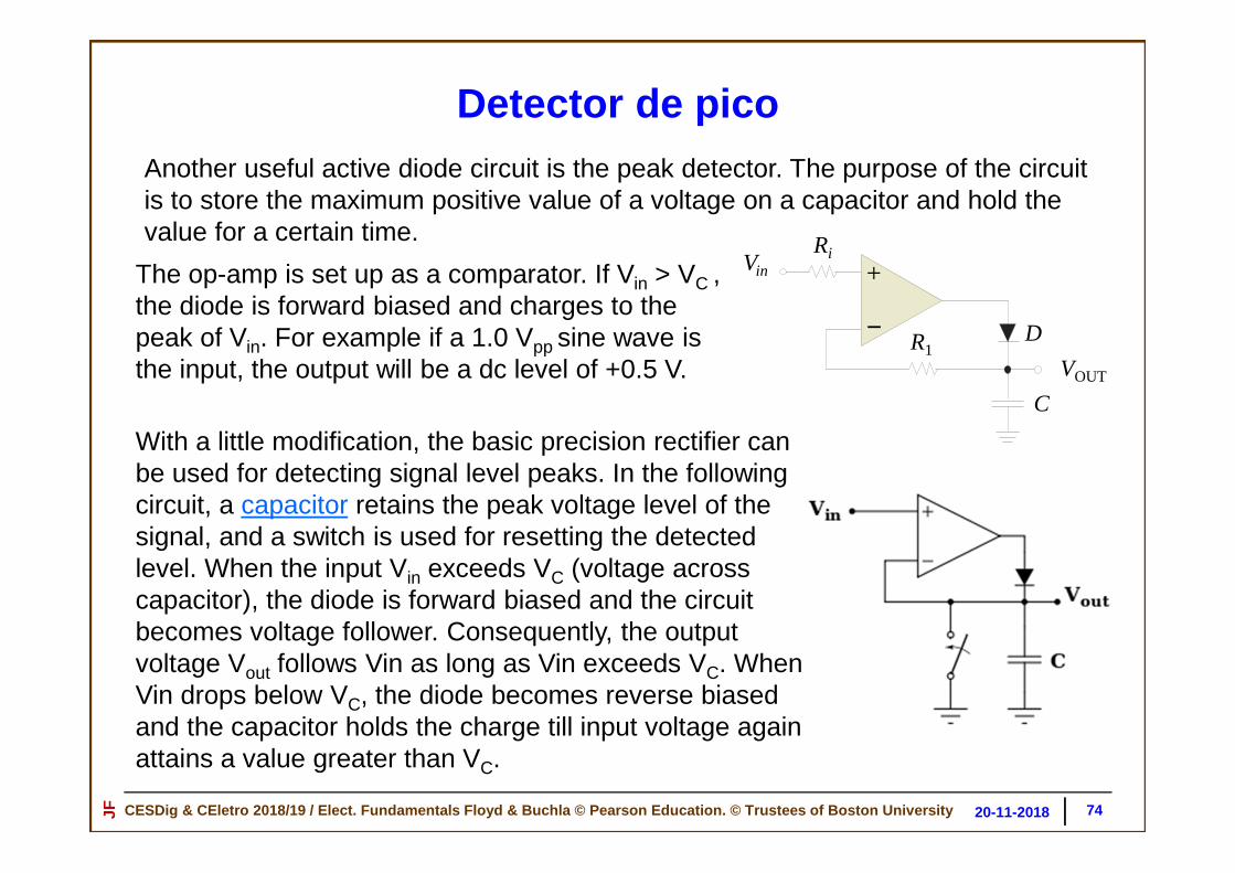
Detector de picoAnother useful active diode circuit is the peak detector. The purpose of the circuit is to store the maximum positive value of a voltage on a capacitor and hold the value for a certain time.
+
−R1
Ri
C
Vin
D
VOUT
The op-amp is set up as a comparator. If Vin > VC ,the diode is forward biased and charges to the peak of Vin. For example if a 1.0 Vpp sine wave is the input, the output will be a dc level of +0.5 V.
With a little modification, the basic precision rectifier can be used for detecting signal level peaks. In the following circuit, a capacitor retains the peak voltage level of the signal, and a switch is used for resetting the detected level. When the input Vin exceeds VC (voltage across capacitor), the diode is forward biased and the circuit becomes voltage follower. Consequently, the output voltage Vout follows Vin as long as Vin exceeds VC. When Vin drops below VC, the diode becomes reverse biased and the capacitor holds the charge till input voltage again attains a value greater than VC.
20-11-2018

CESDig & CEletro 2018/19 / Elect. Fundamentals Floyd & Buchla © Pearson Education. © Trustees of Boston U niversityJF
Comparadores e detetores de nível
7520-11-2018

CESDig & CEletro 2018/19 / Elect. Fundamentals Floyd & Buchla © Pearson Education. © Trustees of Boston U niversityJFUm amplificador operacional tem um ganho em
malha aberta muito elevadoSem realimentação negativa, uma diferença extremamente pequena (>~10 µV) entre as tensões aplicadas às entradas, levam o AmpOp para fora dos seus “limites” e tornam-no não-linear
Terminal da entrada não inversora
7620-11-2018
8 !
8
8
8
8
!
!Terminal de entrada inversora

CESDig & CEletro 2018/19 / Elect. Fundamentals Floyd & Buchla © Pearson Education. © Trustees of Boston U niversityJFDetetor de zero
7720-11-2018
Quando a tensão aplicada à entrada não inversora passa por zero, a saída do AmpOp comuta entre os seus valores de saturação. Desta forma o circuito detecta que a tensão tomou o valor zero.
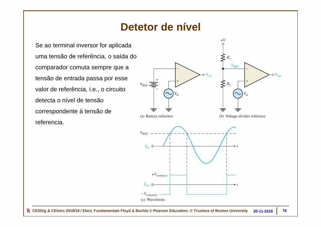
CESDig & CEletro 2018/19 / Elect. Fundamentals Floyd & Buchla © Pearson Education. © Trustees of Boston U niversityJFDetetor de nível
7820-11-2018
Se ao terminal inversor for aplicada
uma tensão de referência, o saída do
comparador comuta sempre que a
tensão de entrada passa por esse
valor de referência, i.e., o circuito
detecta o nível de tensão
correspondente à tensão de
referencia.

CESDig & CEletro 2018/19 / Elect. Fundamentals Floyd & Buchla © Pearson Education. © Trustees of Boston U niversityJF
Comparators
Op-amps can be used to compare the amplitude of one voltage with another. Although general-purpose op-amps can be used as comparators, special op-amps are available to optimize speed and add features.
An example of a comparison circuit is shown. The input is compared with a reference set by the voltage-divider. Notice that there is no feedback; the op-amp is operated in open-loop, so the output will be in saturation.
Vin
R1
Vout
+
−
R2
+V
Comparador
7920-11-2018

CESDig & CEletro 2018/19 / Elect. Fundamentals Floyd & Buchla © Pearson Education. © Trustees of Boston U niversityJF
Esboce a saída do comparador em relação à entrada; assuma que a tensão máxima na saída é ±13 V.
Vin
R1
Vout+
−
R2
V = +15 V
10 kΩ
3.9 kΩ
O valor de referência é +4.2 V. A saída estará saturada positivamente sempre que Vin > +4.2 V
Vin
+10 V
−10 V
0 V+4.2 V
+13 V
−13 V
0 V
Comparador
8020-11-2018
CESDig & CEletro 2018/19 / Elect. Fundamentals Floyd & Buchla © Pearson Education. © Trustees of Boston U niversityJF
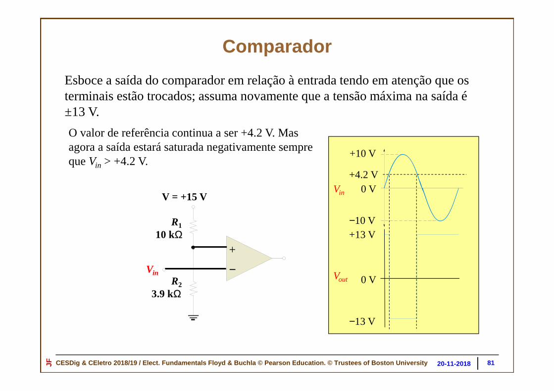
Esboce a saída do comparador em relação à entrada tendo em atenção que os terminais estão trocados; assuma novamente que a tensão máxima na saída é ±13 V.
Vin
R1
Vout
+
−R2
V = +15 V
10 kΩ
3.9 kΩ
O valor de referência continua a ser +4.2 V. Mas agora a saída estará saturada negativamente sempre que Vin > +4.2 V.
Vin
+10 V
−10 V
0 V+4.2 V
+13 V
−13 V
0 V
Comparador
8120-11-2018

CESDig & CEletro 2018/19 / Elect. Fundamentals Floyd & Buchla © Pearson Education. © Trustees of Boston U niversityJF
Circuitos não lineares
Comparadores com realimentação positiva
(ver também guia do trabalho 10)
8227-11-2018

CESDig & CEletro 2018/19 / Elect. Fundamentals Floyd & Buchla © Pearson Education. © Trustees of Boston U niversityJFAmpOp sem realimentação/retroação
83
8 !
!
O ampOp sem realimentação/retroação comporta-se como um circuito comparador, comprando a tensão de um terminal com a tensão do outro, produzindo à saída um sinal que multiplica a diferença entre os dois sinais pelo ganho em malha aberta do AmpOp.
Como o ganho do AmpOp em malha aberta é, em geral, muito elevado, o amplificador entra facilmente em saturação, tomando a saída um dos valores possíveis:
8 'TU se V !
8 = −'TU! se ! V
27-11-2018
@≅0
@!≅0
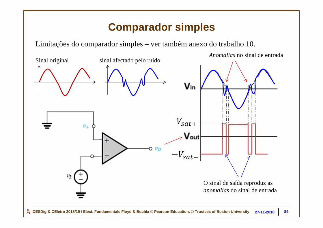
CESDig & CEletro 2018/19 / Elect. Fundamentals Floyd & Buchla © Pearson Education. © Trustees of Boston U niversityJFComparador simples
84
Limitações do comparador simples – ver também anexo do trabalho 10.Anomalias no sinal de entrada
O sinal de saída reproduz as anomalias do sinal de entrada
'TU!
'TU
Sinal original sinal afectado pelo ruido
27-11-2018
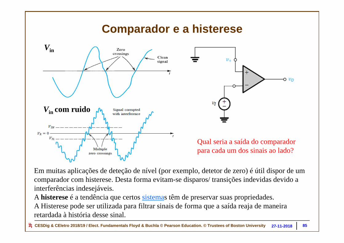
CESDig & CEletro 2018/19 / Elect. Fundamentals Floyd & Buchla © Pearson Education. © Trustees of Boston U niversityJFComparador e a histerese
85
Qual seria a saída do comparador para cada um dos sinais ao lado?
Vin
27-11-2018
Vin com ruido
Em muitas aplicações de deteção de nível (por exemplo, detetor de zero) é útil dispor de um comparador com histerese. Desta forma evitam-se disparos/ transições indevidas devido a interferências indesejáveis. A histereseé a tendência que certos sistemas têm de preservar suas propriedades. A Histerese pode ser utilizada para filtrar sinais de forma que a saída reaja de maneira retardada à história desse sinal.

CESDig & CEletro 2018/19 / Elect. Fundamentals Floyd & Buchla © Pearson Education. © Trustees of Boston U niversityJFComparador “Schmitt trigger”
comparador com histerese
86
Este circuito comparador muda de estado a diferentes valores de vI , dependendo de vI
estar a aumentar ou a diminuir. A comutação entre os estado L+ e L- depende do passado do sinal. Diz-se que o circuito apresenta histerese.
W 'TU
W! 'TU!
27-11-2018
Malha de realimentação positiva “Estado alto” ou “1”
“Estado baixo” ou “0”W! 'TU!W 'TU

CESDig & CEletro 2018/19 / Elect. Fundamentals Floyd & Buchla © Pearson Education. © Trustees of Boston U niversityJF
A realimentação num amplificador consiste em reintroduzir uma parte do sinal de saída na entrada. Dependendo da(s) malha(s) exterior(es), a realimentação pode reforçar o sinal de entrada, ou contrariá-lo. A realimentação positiva corresponde a um reforço do sinal de entrada pela saída.
Av
Feedback circuit
87
Realimentação positiva(feedback positivo)
B
Acl = AvB
Av+vin vout
Av =ganho em malha aberta/sem realimentação
Acl,f = ganho em malha fechada/com realimentação
B = factor de realimentação
+vin vout
1 −
= ≡
v+-
= +
vfvf
= +
27-11-2018

CESDig & CEletro 2018/19 / Elect. Fundamentals Floyd & Buchla © Pearson Education. © Trustees of Boston U niversityJFComparador “Schmitt trigger”
88
Consideremos vI negativa (|vI|>|v0|/A): tem-se v0=Vsat+=L+ e v+=VTH=Vsat+R1/(R1+R2). Se agora aumentarmos progressivamente vI obtemos a função de transferência do circuito representada abaixo: a tensão v0 muda de v0=Vsat+=L+ para v0=Vsat-=L- quando vI
fica superior a VTH=Vsat+R1/(R1+R2). Notar que, em consequência, a v+ passa a valer v+=VLH= -Vsat-R1/(R1+R2).
vI<0
W 'TU
W! 'TU!
27-11-2018
W! 'TU! estado baixo ou “0”
W 'TU estado alto ou “1”

CESDig & CEletro 2018/19 / Elect. Fundamentals Floyd & Buchla © Pearson Education. © Trustees of Boston U niversityJFComparador “Schmitt trigger”
89
Consideremos agora vI positiva (|vI|>|v0|/A): tem-se v0=-Vsat-=L- e v-=VLH=-Vsat- R1/(R1+R2). Se agora diminuirmos progressivamente vI obtemos a função de transferência do circuito representada abaixo: a tensão v0 muda de v0= -Vsat-=L- para v0=+Vsat+=L+ quando vI fica inferior a VLH=-Vsat- R1/(R1+R2). Notar que, em consequência, v+ passa a valer v+=VTH=Vsat+
R1/(R1+R2).
vI>0
W 'TU
W! 'TU!
27-11-2018

CESDig & CEletro 2018/19 / Elect. Fundamentals Floyd & Buchla © Pearson Education. © Trustees of Boston U niversityJFComparador “Schmitt trigger”
90
O circuito comparador muda de estado a diferentes valores de vI , dependendo de vI
estar a aumentar ou a diminuir. Diz-se que o circuito apresenta histerese. A largura da janela de histerese é a diferença entre VTH e VLH:
LH=R1/(R1+R2)(Vsat+-Vsat-)
W 'TU
W! 'TU!
27-11-2018
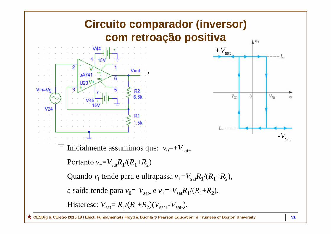
CESDig & CEletro 2018/19 / Elect. Fundamentals Floyd & Buchla © Pearson Education. © Trustees of Boston U niversityJF 91
v0
+
−
R1
R2
vI
Inicialmente assumimos que: v0=+Vsat+
Portanto v+=VsatR1/(R1+R2)
Quando vI tende para e ultrapassa v+=VsatR1/(R1+R2),
a saída tende para v0=-Vsat-e v+=-VsatR1/(R1+R2).
Histerese: Vsat= R1/(R1+R2)(Vsat+-Vsat-).
+Vsat+
-Vsat-
Circuito comparador (inversor) com retroação positiva
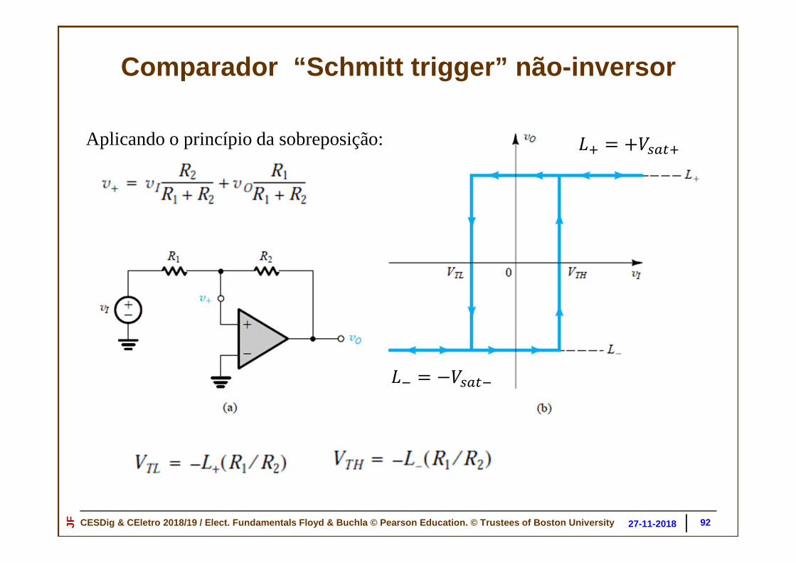
CESDig & CEletro 2018/19 / Elect. Fundamentals Floyd & Buchla © Pearson Education. © Trustees of Boston U niversityJFComparador “Schmitt trigger” não -inversor
92
W 'TU
W! 'TU!
27-11-2018
Aplicando o princípio da sobreposição:
CESDig & CEletro 2018/19 / Elect. Fundamentals Floyd & Buchla © Pearson Education. © Trustees of Boston U niversityJF
Circuitos não lineares e geradores de funções
Osciladores
(ver também guia do trabalho 10)
93

CESDig & CEletro 2018/19 / Elect. Fundamentals Floyd & Buchla © Pearson Education. © Trustees of Boston U niversityJFConceitos básicos de um oscilador sinusoidal
FIGURE 17–52
94
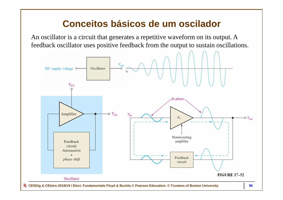
An oscillator is a circuit that generates a repetitive waveform on its output. A feedback oscillator uses positive feedback from the output to sustain oscillations.
The basic oscillator concept showing a sinusoidal output waveform.

CESDig & CEletro 2018/19 / Elect. Fundamentals Floyd & Buchla © Pearson Education. © Trustees of Boston U niversityJFAmpOp com realimentação/retroação positiva
(feedback positivo)
95
B = factor de realimentação ou feedback
1 Casos de interesse aqui: 1 X Y 1
1 ≡
8 Sinais em fase
“Sinais em fase”
Quando BA=1, o ganho torna-se infinito e um sinal não nulo é obtido com Vin=0 , o
circuito produz um sinal periódico (o circuito é um oscilador).
CESDig & CEletro 2018/19 / Elect. Fundamentals Floyd & Buchla © Pearson Education. © Trustees of Boston U niversityJFConceitos básicos de um oscilador
FIGURE 17–52
96
An oscillator is a circuit that generates a repetitive waveform on its output. A feedback oscillator uses positive feedback from the output to sustain oscillations.

CESDig & CEletro 2018/19 / Elect. Fundamentals Floyd & Buchla © Pearson Education. © Trustees of Boston U niversityJFCondições para obter oscilação
FIGURE 17–56
97
When oscillation starts at t0, the condition Acl > 1 causes the output voltage amplitude to build up to a desired level, where Acl decreases to 1 and maintains the desired amplitude.

CESDig & CEletro 2018/19 / Elect. Fundamentals Floyd & Buchla © Pearson Education. © Trustees of Boston U niversityJFOsciladores - Critério de Barkhausen
98
Feedback oscillators
An oscillator is a circuit that generates a repetitive waveform on its output. A feedback oscillator uses positive feedback from the output to sustain oscillations.
Av
Conditions for oscillations are
1. The phase shift around the loop must be 0o.
2. The closed loop gain must be 1 (unity gain).
B
Acl = AvB = 1
Av
Feedback circuit
Critério de Barkhausen: para que a oscilação se mantenha, o módulo do ganho da malha de realimentação deve ser igual à unidade, e dd fase entre !e deve ser zero ou um multiplo inteiro de 2[.
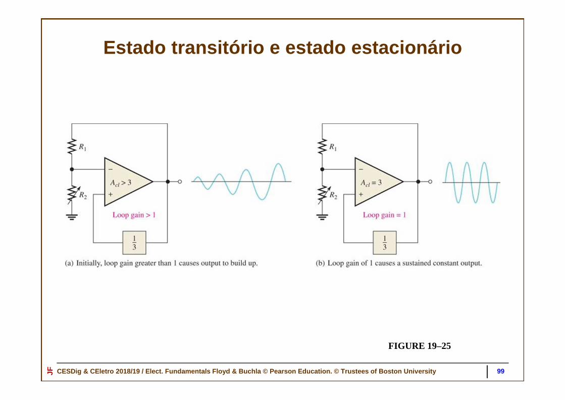
CESDig & CEletro 2018/19 / Elect. Fundamentals Floyd & Buchla © Pearson Education. © Trustees of Boston U niversityJFEstado transitório e estado estacionário
FIGURE 19–25
99
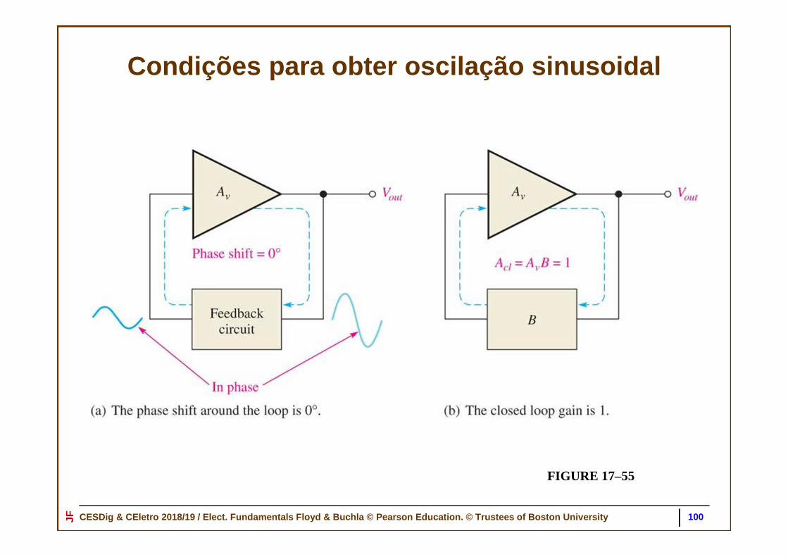
CESDig & CEletro 2018/19 / Elect. Fundamentals Floyd & Buchla © Pearson Education. © Trustees of Boston U niversityJFCondições para obter oscilação sinusoidal
FIGURE 17–55
100

CESDig & CEletro 2018/19 / Elect. Fundamentals Floyd & Buchla © Pearson Education. © Trustees of Boston U niversityJFGerador em relaxação de onda quadrada
101
8 !

CESDig & CEletro 2018/19 / Elect. Fundamentals Floyd & Buchla © Pearson Education. © Trustees of Boston U niversityJF 102
Gerador em relaxação de onda quadradaThe square-wave relaxation oscillator uses a comparator to switch the output based on the charging and discharging of a capacitor.
CVout
+
−
R1
R2
R
Vout
Cv+
v-
X *
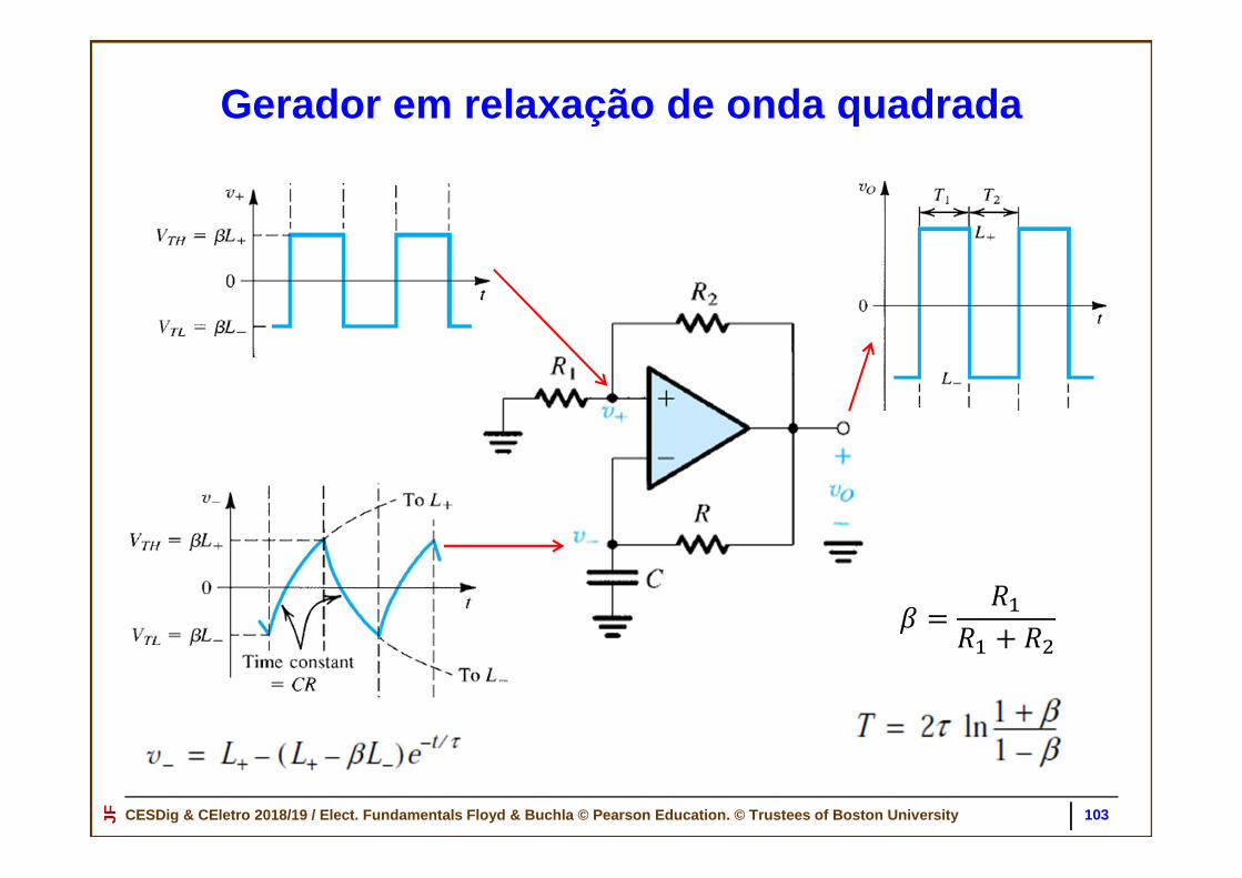
CESDig & CEletro 2018/19 / Elect. Fundamentals Floyd & Buchla © Pearson Education. © Trustees of Boston U niversityJF 103
Gerador em relaxação de onda quadrada
X *

CESDig & CEletro 2018/19 / Elect. Fundamentals Floyd & Buchla © Pearson Education. © Trustees of Boston U niversityJF 104
Gerador de onda triangularA triangular-wave oscillator can be made from a comparator and an integrator. The integrator produces a ramp due to the constant current charging of the capacitor. When the ramp reaches a trip point, the comparator suddenly switches to opposite level and the ramp changes direction.
Vout (triangle)
Vout (square)
Comparator Integrator
+
−+
−
R3
R2
R1
C

CESDig & CEletro 2018/19 / Elect. Fundamentals Floyd & Buchla © Pearson Education. © Trustees of Boston U niversityJFOscilador de onda quadrada com dois AmpOPs
FIGURE 19–28
105
Waveforms for the circuit
FIGURE 19–29

CESDig & CEletro 2018/19 / Elect. Fundamentals Floyd & Buchla © Pearson Education. © Trustees of Boston U niversityJF
Amplificadores
Revisão/clarificação de conceitos
10613-11-2018

CESDig & CEletro 2018/19 / Elect. Fundamentals Floyd & Buchla © Pearson Education. © Trustees of Boston U niversityJFCircuito amplificador
107

CESDig & CEletro 2018/19 / Elect. Fundamentals Floyd & Buchla © Pearson Education. © Trustees of Boston U niversityJFGanho em tensão, em corrente e em potência
de um amplificador
108
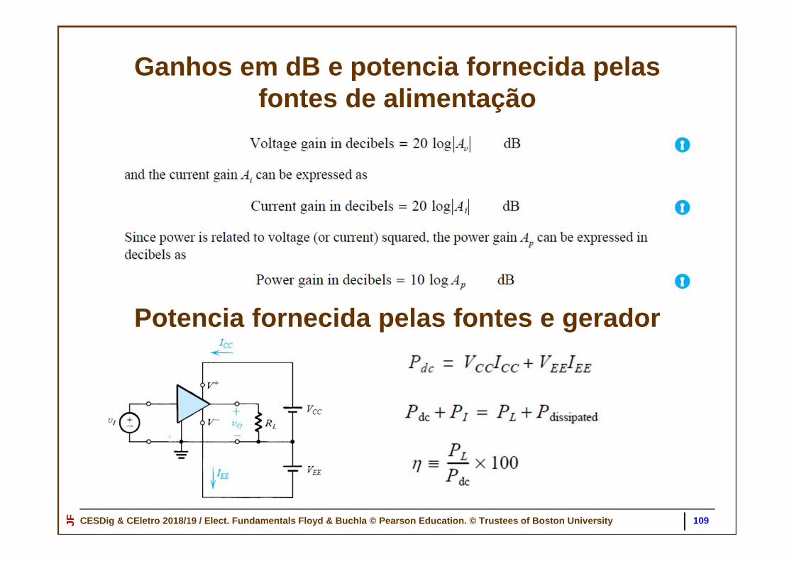
CESDig & CEletro 2018/19 / Elect. Fundamentals Floyd & Buchla © Pearson Education. © Trustees of Boston U niversityJFGanhos em dB e potencia fornecida pelas
fontes de alimentação
109
Potencia fornecida pelas fontes e gerador

CESDig & CEletro 2018/19 / Elect. Fundamentals Floyd & Buchla © Pearson Education. © Trustees of Boston U niversityJFAmplificador em saturação
110

CESDig & CEletro 2018/19 / Elect. Fundamentals Floyd & Buchla © Pearson Education. © Trustees of Boston U niversityJFModelos de pequeno sinal
111
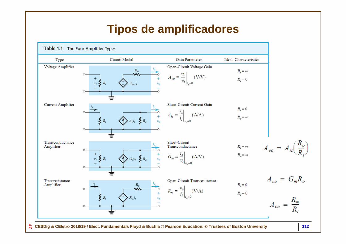
CESDig & CEletro 2018/19 / Elect. Fundamentals Floyd & Buchla © Pearson Education. © Trustees of Boston U niversityJFTipos de amplificadores
112

CESDig & CEletro 2018/19 / Elect. Fundamentals Floyd & Buchla © Pearson Education. © Trustees of Boston U niversityJFDeterminação da resistência de saída (R o)
113

CESDig & CEletro 2018/19 / Elect. Fundamentals Floyd & Buchla © Pearson Education. © Trustees of Boston U niversityJFResposta em frequência
114
Resposta do amplificador seguidor a um sinal sinuso idal de alta frequência
A taxa de atraso (slew rate) do AmpOplimita a resposta em alta frequência das montagens: ver figuras abaixo

CESDig & CEletro 2018/19 / Elect. Fundamentals Floyd & Buchla © Pearson Education. © Trustees of Boston U niversityJF
Amplificadores de transimpedância,
de corrente e
de transadmitância
11513-11-2018

CESDig & CEletro 2018/19 / Elect. Fundamentals Floyd & Buchla © Pearson Education. © Trustees of Boston U niversityJFAmplificador de tensão
(montagem inversora simples)
116
Ganhoemtensão:, `aResistência de entrada:
Resistência de saída: 8 8

CESDig & CEletro 2018/19 / Elect. Fundamentals Floyd & Buchla © Pearson Education. © Trustees of Boston U niversityJFAmplificador transimpedância
(entrada em corrente, saída em tensão)
117
A montagem abaixo é um amplificador transimpedância (ti, i→v), com a ganho V0/Iin :
A resistência de entrada Rin(I) é igual a zero.
A resistência de saída é também igual a zero.
−
+
Iin
Rf
Vout
06-11-2018
' @,, '@
Iin
+
−
*.b (.( .b * ( 1 `c, * ( 1 *)

CESDig & CEletro 2018/19 / Elect. Fundamentals Floyd & Buchla © Pearson Education. © Trustees of Boston U niversityJFAmplificador de corrente
118
O ganho da montagem é -1
Rin(I) é igual a zero.
R0(I) é muito grande (infinita )
Nesta montagem, a corrente Ioutnão depende da carga (RL).
06-11-2018
−
+
Iin
Rf
IoutRL
Iin
+
−
@ @, , @@ 1
As montagens abaixo corresponde a amplificadores de corrente (i), com a ganho Iout/Iin :
Iout
@ @(
, 1 *) , , 0, 8 ∞
Carga flutuante
Nesta montagem a carga (R4) tem de estar flutuante.

CESDig & CEletro 2018/19 / Elect. Fundamentals Floyd & Buchla © Pearson Education. © Trustees of Boston U niversityJFAmplificador de Transadmitância
(entrada em corrente, saída em tensão)
119
A resistência de entrada Rin(I) é muito grande (infinita).
A resistência de saída R0(I) é muito grande (infinita).
06-11-2018
−
+
VinRL
Ri
A
IoutB
' '! '
@ @ '
, =@
'
=1
+
−
Curto-circuito virtual
IRi
A montagem abaixo é um amplificador transadmitência (ta), com a ganho Iout/Vin:

CESDig & CEletro 2018/19 / Elect. Fundamentals Floyd & Buchla © Pearson Education. © Trustees of Boston U niversityJF
Amplificador de instrumentação
120

CESDig & CEletro 2018/19 / Elect. Fundamentals Floyd & Buchla © Pearson Education. © Trustees of Boston U niversityJF 121
Amplificador de instrumentaçãoUma desvantagem da montagem subtratora convencional é que a impedância vista de cada uma das entradas é diferente. O circuito abaixo remove esta desvantagem, fazendo com que a impedância vista de ambas as entradas seja muito grande (→infinito), e permite a introdução de ganho diferencial (i.e., o ganho é igual para ambas as entradas). Esta montagem pode ser usada para medir/amplificar pequenas diferenças entre sinais, sendo por isso usado em muitos instrumentos. Por isso é conhecida como amplificador de instrumentação. É o circuito base, por exemplo, do eletrocardiógrafo.
CESDig & CEletro 2018/19 / Elect. Fundamentals Floyd & Buchla © Pearson Education. © Trustees of Boston U niversityJF 122
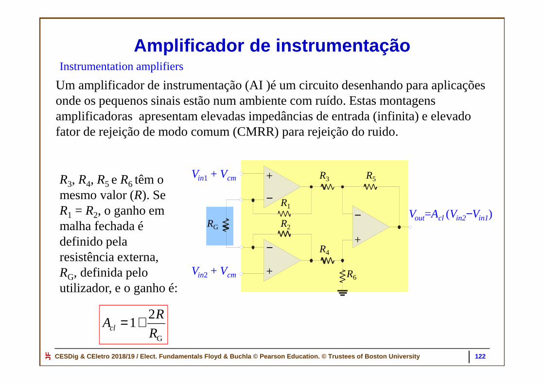
Amplificador de instrumentaçãoInstrumentation amplifiers
Um amplificador de instrumentação (AI )é um circuito desenhando para aplicações onde os pequenos sinais estão num ambiente com ruído. Estas montagens amplificadoras apresentam elevadas impedâncias de entrada (infinita) e elevado fator de rejeição de modo comum (CMRR) para rejeição do ruido.
R3, R4, R5 e R6 têm o mesmo valor (R). Se R1 = R2, o ganho em malha fechada é definido pela resistência externa, RG, definida pelo utilizador, e o ganho é:
G
21cl
RA
R= +
R1
Vin1 + Vcm
R2
R3
R4
R5
R6
+
−
+
−
+
−
Vin2 + Vcm
Vout=Acl (Vin2−Vin1)RG

CESDig & CEletro 2018/19 / Elect. Fundamentals Floyd & Buchla © Pearson Education. © Trustees of Boston U niversityJF 123
Amplificador de instrumentação
Instrumentation amplifiers
G
21cl
RA
R= +
R1
Vin1
R2
R3
R4
R5
R6
+
−
+
−
+
−
Vin2
VoutRG
Consideremos R1 = R2 = 10 kΩ, qual deve ser o valor de RG para que o ganho seja 40?
G
2
1cl
RR
A=
−
Resolvendo em ordem a RG,
( )G
2 10 k
40 1R
Ω= =
− 513 Ω
(510 Ω é o valor standard mais próximo).
CESDig & CEletro 2018/19 / Elect. Fundamentals Floyd & Buchla © Pearson Education. © Trustees of Boston U niversityJF 124
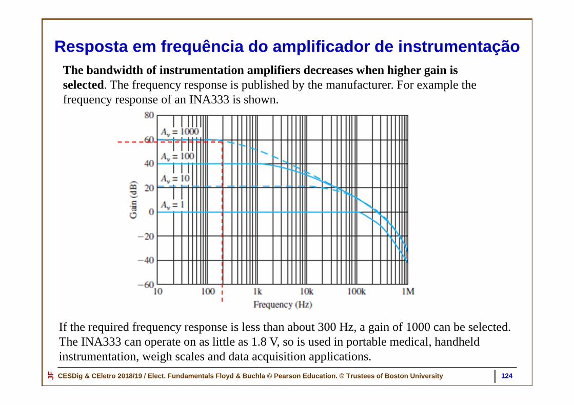
Resposta em frequência do amplificador de instrumen taçãoThe bandwidth of instrumentation amplifiers decreases when higher gain is selected. The frequency response is published by the manufacturer. For example the frequency response of an INA333 is shown.
If the required frequency response is less than about 300 Hz, a gain of 1000 can be selected. The INA333 can operate on as little as 1.8 V, so is used in portable medical, handheld instrumentation, weigh scales and data acquisition applications.

CESDig & CEletro 2018/19 / Elect. Fundamentals Floyd & Buchla © Pearson Education. © Trustees of Boston U niversityJF
Conceitos e parâmetros
de amplificadores operacionais
(ver também guias dos trabalhos práticos)
125

CESDig & CEletro 2018/19 / Elect. Fundamentals Floyd & Buchla © Pearson Education. © Trustees of Boston U niversityJFMontagens com ampops em malha aberta
Detetor de zero Amplificador diferencial Modo comum
126
CESDig & CEletro 2018/19 / Elect. Fundamentals Floyd & Buchla © Pearson Education. © Trustees of Boston U niversityJFParâmetros do AmOp
127
Some important op-amp parameters are:
Input bias current:
Differential input resistance:
Common-mode input resistance:
Input offset current:
Average of input currents required to bias the first stage of the amplifier:
Total resistance between the inverting and non-inverting inputs
Total resistance between each input and ground.
Absolute difference between the two bias currents:
1 2BIAS 2
I II
+=
OS 1 2I I I= −
Output resistance:
Common-mode input voltage range:
The resistance when viewed from the output terminal.
Range of input voltages, which, when applied to both inputs, will not cause clipping or other distortion.
CESDig & CEletro 2018/19 / Elect. Fundamentals Floyd & Buchla © Pearson Education. © Trustees of Boston U niversityJFParâmetros do AmOp
128
Op-amp parameters
Output resistance:
Common-mode input voltage range:
Common-mode rejection ratio
Slew rate:
The resistance when viewed from the output terminal.
Range of input voltages, which, when applied to both inputs, will not cause clipping or other distortion.
Ratio of the differential gain to the common-mode gain. The differential gain for the op-amp by itself is the same as its open loop gain.
( )CMRR v d ol
cm cm
A A
A A= =
The maximum rate of change of the output in response to a step input voltage.

CESDig & CEletro 2018/19 / Elect. Fundamentals Floyd & Buchla © Pearson Education. © Trustees of Boston U niversityJFFator de rejeição em modo comum
129
Common-Mode Rejection Ratio (CMRR)
Many times, noise sources will induce an unwanted voltage in a signal line. When the noise is induced in common-mode, the differential amplifier tends to cancel it. (The diff-amp cannot reject any signal that is in differential mode.)
The ability to reject common-mode signals is measured with a parameter called the common-mode rejection ratio (CMRR), which is defined as
( )CMRR v d
cm
A
A=
CMRR can be expressed in decibels as ( )CMRR 20log v d
cm
A
A
=

CESDig & CEletro 2018/19 / Elect. Fundamentals Floyd & Buchla © Pearson Education. © Trustees of Boston U niversityJFFator de rejeição em modo comum
130
Common-Mode Rejection Ratio (CMRR)
From the defining equation for CMRR:
( ) 500CMRR
0.1v d
cm
A
A= = =
Expressed in decibels, it is
( )( )CMRR 20log 20log 5000v d
cm
A
A
= = =
A certain diff-amp has a differential voltage gain of 500 and a common-mode gain of 0.1. What is the CMRR?
5000
74 dB

CESDig & CEletro 2018/19 / Elect. Fundamentals Floyd & Buchla © Pearson Education. © Trustees of Boston U niversityJFFator de rejeição em modo comum
131
Common-Mode Rejection Ratio (CMRR)
The differential signal is amplified by 100. Therefore, the signal output is
Vout = Av(d) x Vin = 100 x 50 mV =
( )
4.5
100 100 1000.0032
CMRR 90 dB 10 31,600v d
cm
AA = = = = =
A certain diff-amp has Ad = 100 and a CMRR of 90 dB. Describe the output if the input is a 50 mV differential signal and a common mode noise of 1.0 V is present.
The common-mode gain can be found by
The noise is amplified by 0.0032. Therefore, Vnoise = Acm x Vin = 0.0032 x 1.0 V = 3.2 mV
5.0 V
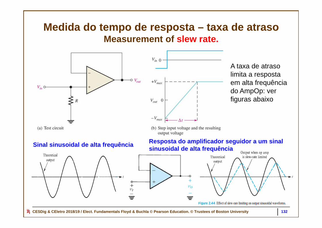
CESDig & CEletro 2018/19 / Elect. Fundamentals Floyd & Buchla © Pearson Education. © Trustees of Boston U niversityJFMedida do tempo de resposta – taxa de atraso
Measurement of slew rate.
132
A taxa de atraso limita a resposta em alta frequência do AmpOp: ver figuras abaixo
Sinal sinusoidal de alta frequência Resposta do amplificador seguidor a um sinal sinusoidal de alta frequência

CESDig & CEletro 2018/19 / Elect. Fundamentals Floyd & Buchla © Pearson Education. © Trustees of Boston U niversityJFTempo de resposta – taxa de atraso
Slew rateOp-amp parameters
What is the slew rate for the output signal shown in response to a step input?
The output goes from −9 V to +9 V in 1µs.
20 VSlew rate =
25 soutV
t µ∆ = =
∆20 V/µs
133

CESDig & CEletro 2018/19 / Elect. Fundamentals Floyd & Buchla © Pearson Education. © Trustees of Boston U niversityJFTempo de resposta – taxa de atraso
Slew rate
134
Op-amp parameters
The output goes from −10 V to +10 V in 25 µs.
What is the slew rate for the output signal shown in response to a step input?
Vout (V)
1210
−10−12
0
25 µs
20 VSlew rate =
25 soutV
t µ∆ = =
∆0.8 V/µs

CESDig & CEletro 2018/19 / Elect. Fundamentals Floyd & Buchla © Pearson Education. © Trustees of Boston U niversityJF
Amplificador operacional LM741
135
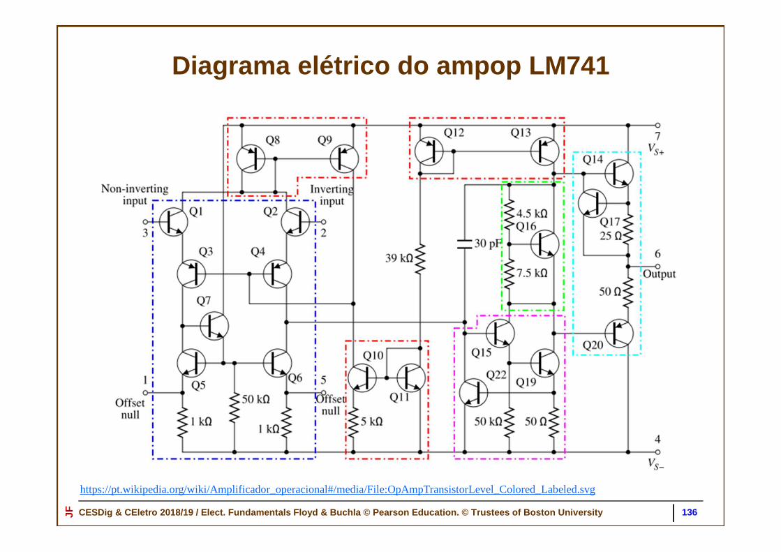
CESDig & CEletro 2018/19 / Elect. Fundamentals Floyd & Buchla © Pearson Education. © Trustees of Boston U niversityJFDiagrama elétrico do ampop LM741
136
https://pt.wikipedia.org/wiki/Amplificador_operacional#/media/File:OpAmpTransistorLevel_Colored_Labeled.svg

CESDig & CEletro 2018/19 / Elect. Fundamentals Floyd & Buchla © Pearson Education. © Trustees of Boston U niversityJFLM741 - Comparação entre AmpOps
137

CESDig & CEletro 2018/19 / Elect. Fundamentals Floyd & Buchla © Pearson Education. © Trustees of Boston U niversityJFSelected Key Terms
138
Operational amplifier
Differential amplifier
Common-mode rejection ratio (CMRR)
An amplifier that produces an output proportional to the difference of two inputs.
A measure of a diff-amp's or op-amp's ability to reject signals that appear the same on both inputs; the ratio of differential voltage gain or open-loop gain (for op-amps) to common-mode gain.
A special type of amplifier exhibiting very high open-loop gain, very high input resistance, very low output resistance, and good rejection of common-mode signals.
Open-loop voltage gain
Closed-loop voltage gain
Noninverting amplifier
Inverting amplifier
An op-amp closed-loop configuration in which the input signal is applied to the noninverting input.
The overall voltage gain of an op-amp with negative feedback.
An op-amp closed-loop configuration in which the input signal is applied to the inverting input.
The internal voltage gain of an op-amp without feedback.

CESDig & CEletro 2018/19 / Elect. Fundamentals Floyd & Buchla © Pearson Education. © Trustees of Boston U niversityJF
Summing amplifier
Averaging amplifier
Scaling adder
An amplifier with several inputs that produces an output voltage proportional to the algebraic sum of the inputs.
A special type of summing amplifier with weighed inputs.
An amplifier with several inputs that produces an output voltage that is the mathematical average of the input voltages.
139
Termos e definições importantes

CESDig & CEletro 2018/19 / Elect. Fundamentals Floyd & Buchla © Pearson Education. © Trustees of Boston U niversityJF
Integrator
Differentiator
Active filter
Series regulator
A frequency selective circuit consisting of active devices such as transistors or op-amps combined with reactive (RC) circuits.
A circuit that produces an inverted output that approaches the mathematical integral of the input.
A circuit that produces an inverted output that approaches the mathematical derivative of the input, which is the rate of change.
A type of voltage regulator with the control element in series between the input and output.
140
Termos e definições importantes
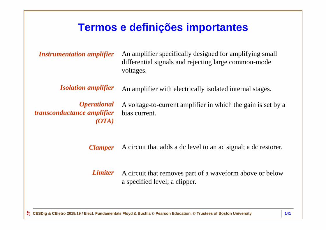
CESDig & CEletro 2018/19 / Elect. Fundamentals Floyd & Buchla © Pearson Education. © Trustees of Boston U niversityJF 141
Termos e definições importantes
Instrumentation amplifier
Isolation amplifier
Operational transconductance amplifier
(OTA)
An amplifier specifically designed for amplifying small differential signals and rejecting large common-mode voltages.
A voltage-to-current amplifier in which the gain is set by a bias current.
An amplifier with electrically isolated internal stages.
Clamper
Limiter
A circuit that adds a dc level to an ac signal; a dc restorer.
A circuit that removes part of a waveform above or below a specified level; a clipper.

CESDig & CEletro 2018/19 / Elect. Fundamentals Floyd & Buchla © Pearson Education. © Trustees of Boston U niversityJF 142

CESDig & CEletro 2018/19 / Elect. Fundamentals Floyd & Buchla © Pearson Education. © Trustees of Boston U niversityJFRepresentações esquemáticas do AmpOp
143

CESDig & CEletro 2018/19 / Elect. Fundamentals Floyd & Buchla © Pearson Education. © Trustees of Boston U niversityJFMontagem não inversora
144
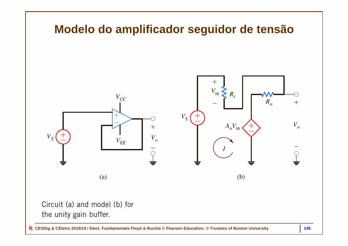
CESDig & CEletro 2018/19 / Elect. Fundamentals Floyd & Buchla © Pearson Education. © Trustees of Boston U niversityJFModelo do amplificador seguidor de tensão
145

CESDig & CEletro 2018/19 / Elect. Fundamentals Floyd & Buchla © Pearson Education. © Trustees of Boston U niversityJFMontagem inversora
146
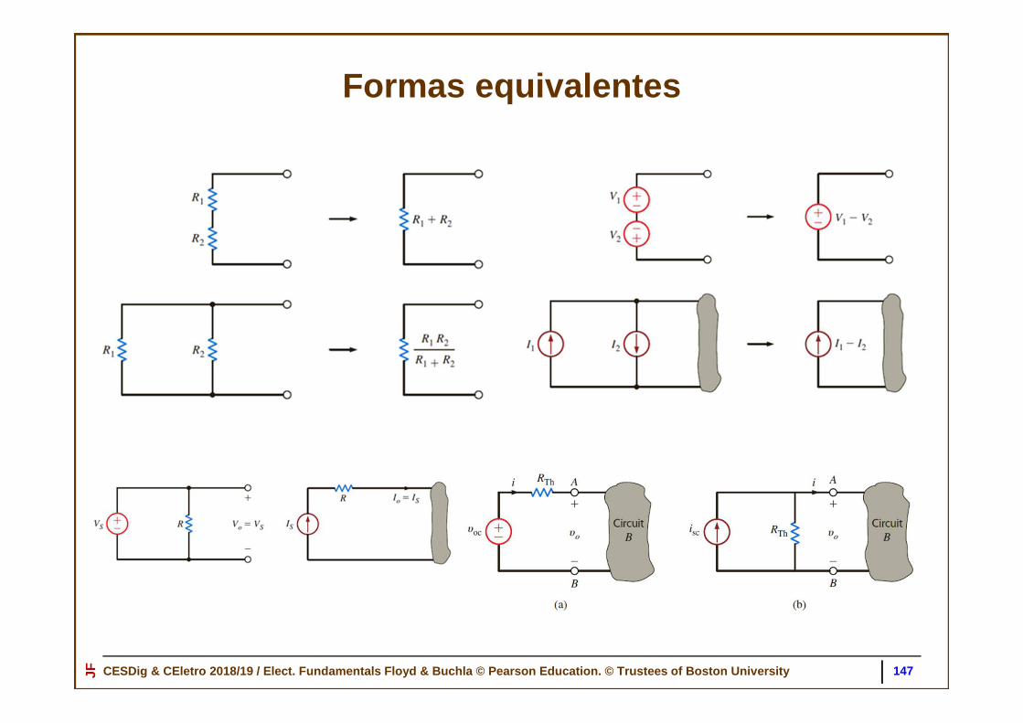
CESDig & CEletro 2018/19 / Elect. Fundamentals Floyd & Buchla © Pearson Education. © Trustees of Boston U niversityJFFormas equivalentes
147

CESDig & CEletro 2018/19 / Elect. Fundamentals Floyd & Buchla © Pearson Education. © Trustees of Boston U niversityJFCircuito RLC usado para simular a queda da ponte
Tacoma Narrows
148
https://www.youtube.com/watch?v=ESTJCQpGW3Q

CESDig & CEletro 2018/19 / Elect. Fundamentals Floyd & Buchla © Pearson Education. © Trustees of Boston U niversityJFCircuito RLC usado para simular a queda da ponte
Tacoma Narrows
149
https://www.youtube.com/watch?v=ESTJCQpGW3Q

CESDig & CEletro 2018/19 / Elect. Fundamentals Floyd & Buchla © Pearson Education. © Trustees of Boston U niversityJFDiagrama do circuito usado para simular a queda
da ponte Tacoma Narrows
150
https://www.youtube.com/watch?v=ESTJCQpGW3Q

CESDig & CEletro 2018/19 / Elect. Fundamentals Floyd & Buchla © Pearson Education. © Trustees of Boston U niversityJFFunção de transferência de alguns AmpOps
151

CESDig & CEletro 2018/19 / Elect. Fundamentals Floyd & Buchla © Pearson Education. © Trustees of Boston U niversityJFElementos básicos de um oscilador sinusoidal
FIGURE 17–53
152

CESDig & CEletro 2018/19 / Elect. Fundamentals Floyd & Buchla © Pearson Education. © Trustees of Boston U niversityJFCondições para obter oscilação
FIGURE 17–54
153

CESDig & CEletro 2018/19 / Elect. Fundamentals Floyd & Buchla © Pearson Education. © Trustees of Boston U niversityJFConceitos básicos de um oscilador sinusoidal
FIGURE 17–52
154
An oscillator is a circuit that generates a repetitive waveform on its output. A feedback oscillator uses positive feedback from the output to sustain oscillations.
The basic oscillator concept showing a sinusoidal output waveform.

CESDig & CEletro 2018/19 / Elect. Fundamentals Floyd & Buchla © Pearson Education. © Trustees of Boston U niversityJF 155