Embed Size (px)
Citation preview
See discussions, stats, and author profiles for this publication at: https://www.researchgate.net/publication/224240045
A 5-GHz Direct Digital Frequency Synthesizer Using an Analog-Sine-Mapping
Technique in 0.35- $\mu$m SiGe BiCMOS
Article in IEEE Journal of Solid-State Circuits · October 2011
DOI: 10.1109/JSSC.2011.2145290 · Source: IEEE Xplore
CITATIONS
19
READS
112
All content following this page was uploaded by Jun-Hong Weng on 25 April 2014.
The user has requested enhancement of the downloaded file.
2064 IEEE JOURNAL OF SOLID-STATE CIRCUITS, VOL. 46, NO. 9, SEPTEMBER 2011
A 5-GHz Direct Digital Frequency SynthesizerUsing an Analog-Sine-Mapping Technique
in 0.35- m SiGe BiCMOSChing-Yuan Yang, Member, IEEE, Jun-Hong Weng, Student Member, IEEE, and Hsuan-Yu Chang
Abstract—A direct digital frequency synthesizer (DDFS) usingan analog-sine-mapping technique is presented in a 0.35- m SiGeBiCMOS process. We intend to apply the translinear principle todevelop a triangle-to-sine converter (TSC) that can achieve out-puts with low harmonic content. The TSC is introduced for theDDFS to translate phase data to sine wave. Using this analog-in-terpolating technique, the DDFS, with 9 bits of phase resolutionand 8 bits of amplitude resolution, can achieve operation at 5-GHzclock frequency and can further reduce power consumption anddie area. The spurious-free dynamic range (SFDR) of the DDFSis better than 48 dBc at low synthesized frequencies, decreasingto 45.7 dBc worst case at the Nyquist synthesized frequency foroutput frequency band (0–2.5 GHz). The DDFS consumes 460 mWat a 3.3-V supply and achieves a high power efficiency figure ofmerit (FOM) of 10.87 GHz/W. The chip occupies mm .
Index Terms—BiCMOS integrated circuits, digital-to-analogconverter, direct digital frequency synthesizer, translinear, tri-angle-to-sine converter.
I. INTRODUCTION
H IGH synthesized frequencies can be achieved usingphase-locked loops (PLLs). However, most PLLs inher-
ently exhibit limited voltage-controlled oscillator tuning range,internal loop delay, and relatively narrowband control loop,thereby limiting the tuning range, tuning speed, and modulationcapability. Nowadays, fast frequency switching is becomingcritically important in modern wireless communication systemssuch as in spread-spectrum communication systems [1]. Toachieve fast switching, direct digital frequency synthesizer(DDFS) has become as an alternative to PLL frequency synthe-sizer since it does not use a feedback loop and hence can providefast frequency switching. In DDFS, all of the signal-processingoperations that synthesize and tune the sine wave are performeddigitally. For state of the art digital communication systems,DDFS can not only provide fine frequency resolution, allowfast settling time and fast frequency hopping performance anddirect phase and frequency modulation in the digital domain,
Manuscript received January 13, 2011; revised March 28, 2011; acceptedApril 02, 2011. Date of publication June 02, 2011; date of current versionAugust24, 2011. This paper was approved by Associate Editor Behzad Razavi. Thiswork was supported by the National Science Council (NSC), Taiwan, R.O.C.,under Contract NSC98-2221-E-005-077.The authors are with the Graduate Institute of Electrical Engineering and
the Department of Electrical Engineering, National Chung Hsing University,Taichung, Taiwan (e-mail: [email protected]).Color versions of one or more of the figures in this paper are available online
at http://ieeexplore.ieee.org.Digital Object Identifier 10.1109/JSSC.2011.2145290
but also has the advantage of low phase noise (roughly equal tothat of the input clock) over PLL approaches. While DDFS canprovide the above features, it is considered a power-hungry cir-cuit, especially for high clock frequencies, resulting in reducedusability for portable wireless communication applications.Thus, it requires entirely new ways of doing electronic circuitdesign to lower power dissipation.Microwave DDFS circuits are mostly designed using indium
phosphide (InP) HBT and silicon germanium (SiGe) HBT tech-nologies. Although there are several DDFSs implemented in InPHBT technologies that have been reported to operate at clockfrequencies from 9 to 30 GHz [2]–[4], the best power-efficiencyfigure-of-merit (FOM) of those DDFSs is 3.39 GHz/W [4]. Onthe other hand, SiGe BiCMOS DDFSs reported in [5]–[8] canwork with multiple gigahertz clock speed, and the best power-efficiency FOM of those SiGe DDFSs arrives at 6.47 GHz/W[6]. All of the above DDFSs used a nonlinear digital-to-analogconverter (DAC) as a sine-to-amplitude converter to achieve thegoal of high speed and low power. However, the nonlinear DACin DDFS requires a sine interpolation algorithm for amplitudetransfer in the hybrid digital and analog domain, leading to acomplex and cumbersome design and even lower output spurnoise performance for DDFS.An alternative approach is to combine a linear DAC and
an analog-sine-mapping circuit in order to replace the roleof the existing nonlinear DAC. Compared to the nonlinearDAC architecture for DDFS, design of the linear DAC is moresimplified and can maintain reasonable spur noise performancewith a given amplitude resolution. The DDFS architecture,using such an approach, may have the benefits of low powerconsumption and high speed operation by mitigating theDAC’s complexity. In [9], a 9-bit DDFS uses the nonlinearfunction of a simple bipolar differential pair to perform ananalog triangle-to-sine conversion. This particular DDFS wasprocessed using 0.25- m BiCMOS technology and achieved apower efficiency of 19.48 GHz/W at 6 GHz. However, whileusing the nonlinear transformation of the differential pair forDDFS, both the peak value and common-mode level of theinput triangulated wave become very critical to the quality ofthe sinusoid output. As a result, due to these transfer errorson the differential pair, the SFDR presented in [9] was merelybelow 30 dBc for most output synthesis frequencies. Moreover,the nonlinear transfer function of the fabricated circuit deeplydepends upon the variations on process, supply voltage andtemperature (PVT), resulting in DAC linearity that is hard tocontrol.
0018-9200/$26.00 © 2011 IEEE
YANG et al.: A 5-GHz DIRECT DIGITAL FREQUENCY SYNTHESIZER USING AN ANALOG-SINE-MAPPING TECHNIQUE IN 0.35- m SiGe BiCMOS 2065
In this work, the analog-sine-mapping conversion circuit isdesigned through the translinear principle to provide low har-monic content for sine output. The proposed conversion cir-cuit has better noise performance with differential current-modeoperation. The output circuits immunity from power-supply-injected and substrate-injected noise sources. For comparison,the proposed DDFS, with 9 bits of phase resolution and 8 bitsof amplitude resolution, can achieve a power-efficiency FOMof 10.87 GHz/W and produce the spurious-free dynamic range(SFDR) of larger than 45.7 dBc in wide output band. This DDFSemploys 0.35- m SiGe BiCMOS, which is less expensive, morecompact, and consumes less power than aforementioned coun-terparts.The paper is organized as follows. Existing DDFS architec-
tures are summarized in Section II. A new DDFS is proposedthat employs the development of a linear DAC and an analogsine-function circuit. The sine-function core, presented inSection III, is based on the translinear principle, which will beshown to provide low harmonic content. This core is composedof only 10 BJTs. The proposed architecture is shown to havesignificant area and power savings at high clock rates. Designconsideration of the other building blocks will be discussed inSection IV. Section V presents measured results of the DDFS,as well as a comparison with recently published works. Finally,concluding remarks are drawn in Section VI.
II. DDFS ARCHITECTURES
A. Conventional DDFS
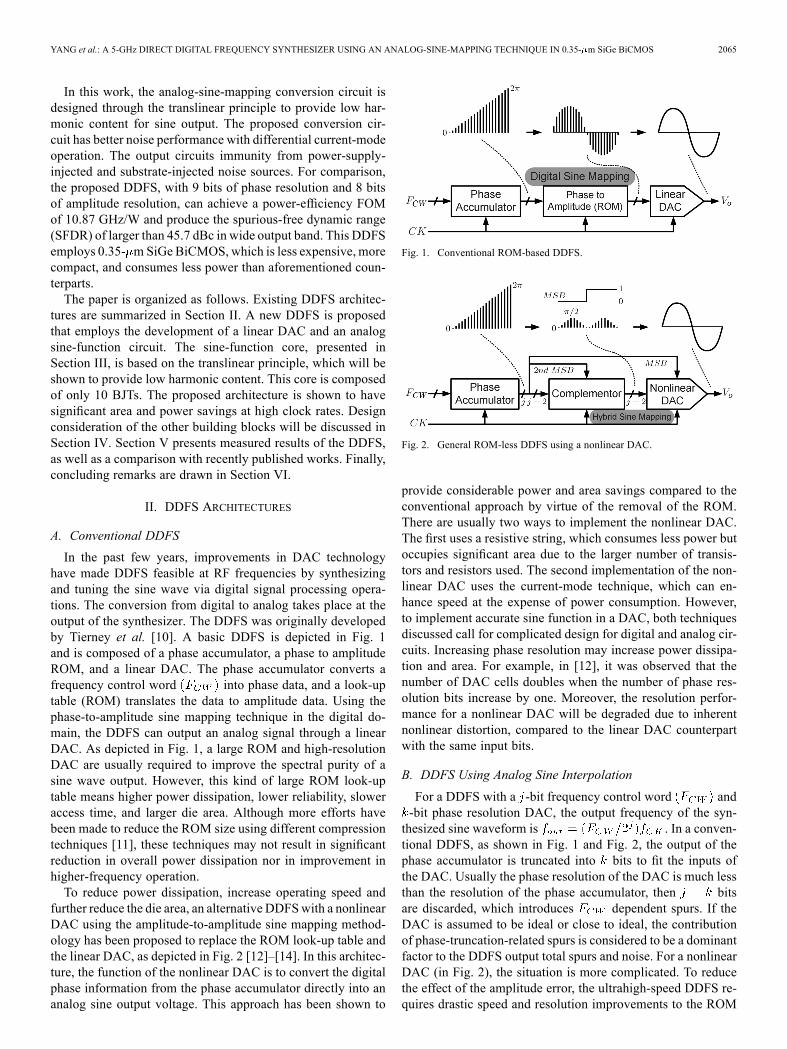
In the past few years, improvements in DAC technologyhave made DDFS feasible at RF frequencies by synthesizingand tuning the sine wave via digital signal processing opera-tions. The conversion from digital to analog takes place at theoutput of the synthesizer. The DDFS was originally developedby Tierney et al. [10]. A basic DDFS is depicted in Fig. 1and is composed of a phase accumulator, a phase to amplitudeROM, and a linear DAC. The phase accumulator converts afrequency control word into phase data, and a look-uptable (ROM) translates the data to amplitude data. Using thephase-to-amplitude sine mapping technique in the digital do-main, the DDFS can output an analog signal through a linearDAC. As depicted in Fig. 1, a large ROM and high-resolutionDAC are usually required to improve the spectral purity of asine wave output. However, this kind of large ROM look-uptable means higher power dissipation, lower reliability, sloweraccess time, and larger die area. Although more efforts havebeen made to reduce the ROM size using different compressiontechniques [11], these techniques may not result in significantreduction in overall power dissipation nor in improvement inhigher-frequency operation.To reduce power dissipation, increase operating speed and
further reduce the die area, an alternative DDFSwith a nonlinearDAC using the amplitude-to-amplitude sine mapping method-ology has been proposed to replace the ROM look-up table andthe linear DAC, as depicted in Fig. 2 [12]–[14]. In this architec-ture, the function of the nonlinear DAC is to convert the digitalphase information from the phase accumulator directly into ananalog sine output voltage. This approach has been shown to
Fig. 1. Conventional ROM-based DDFS.
Fig. 2. General ROM-less DDFS using a nonlinear DAC.
provide considerable power and area savings compared to theconventional approach by virtue of the removal of the ROM.There are usually two ways to implement the nonlinear DAC.The first uses a resistive string, which consumes less power butoccupies significant area due to the larger number of transis-tors and resistors used. The second implementation of the non-linear DAC uses the current-mode technique, which can en-hance speed at the expense of power consumption. However,to implement accurate sine function in a DAC, both techniquesdiscussed call for complicated design for digital and analog cir-cuits. Increasing phase resolution may increase power dissipa-tion and area. For example, in [12], it was observed that thenumber of DAC cells doubles when the number of phase res-olution bits increase by one. Moreover, the resolution perfor-mance for a nonlinear DAC will be degraded due to inherentnonlinear distortion, compared to the linear DAC counterpartwith the same input bits.
B. DDFS Using Analog Sine Interpolation
For a DDFS with a -bit frequency control word and-bit phase resolution DAC, the output frequency of the syn-thesized sine waveform is . In a conven-tional DDFS, as shown in Fig. 1 and Fig. 2, the output of thephase accumulator is truncated into bits to fit the inputs ofthe DAC. Usually the phase resolution of the DAC is much lessthan the resolution of the phase accumulator, then bitsare discarded, which introduces dependent spurs. If theDAC is assumed to be ideal or close to ideal, the contributionof phase-truncation-related spurs is considered to be a dominantfactor to the DDFS output total spurs and noise. For a nonlinearDAC (in Fig. 2), the situation is more complicated. To reducethe effect of the amplitude error, the ultrahigh-speed DDFS re-quires drastic speed and resolution improvements to the ROM
2066 IEEE JOURNAL OF SOLID-STATE CIRCUITS, VOL. 46, NO. 9, SEPTEMBER 2011
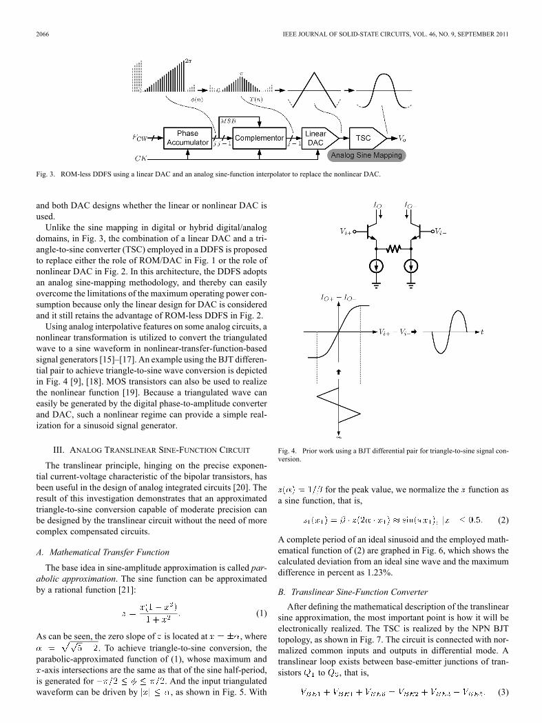
Fig. 3. ROM-less DDFS using a linear DAC and an analog sine-function interpolator to replace the nonlinear DAC.
and both DAC designs whether the linear or nonlinear DAC isused.Unlike the sine mapping in digital or hybrid digital/analog
domains, in Fig. 3, the combination of a linear DAC and a tri-angle-to-sine converter (TSC) employed in a DDFS is proposedto replace either the role of ROM/DAC in Fig. 1 or the role ofnonlinear DAC in Fig. 2. In this architecture, the DDFS adoptsan analog sine-mapping methodology, and thereby can easilyovercome the limitations of the maximum operating power con-sumption because only the linear design for DAC is consideredand it still retains the advantage of ROM-less DDFS in Fig. 2.Using analog interpolative features on some analog circuits, a
nonlinear transformation is utilized to convert the triangulatedwave to a sine waveform in nonlinear-transfer-function-basedsignal generators [15]–[17]. An example using the BJT differen-tial pair to achieve triangle-to-sine wave conversion is depictedin Fig. 4 [9], [18]. MOS transistors can also be used to realizethe nonlinear function [19]. Because a triangulated wave caneasily be generated by the digital phase-to-amplitude converterand DAC, such a nonlinear regime can provide a simple real-ization for a sinusoid signal generator.
III. ANALOG TRANSLINEAR SINE-FUNCTION CIRCUIT
The translinear principle, hinging on the precise exponen-tial current-voltage characteristic of the bipolar transistors, hasbeen useful in the design of analog integrated circuits [20]. Theresult of this investigation demonstrates that an approximatedtriangle-to-sine conversion capable of moderate precision canbe designed by the translinear circuit without the need of morecomplex compensated circuits.
A. Mathematical Transfer Function
The base idea in sine-amplitude approximation is called par-abolic approximation. The sine function can be approximatedby a rational function [21]:
(1)
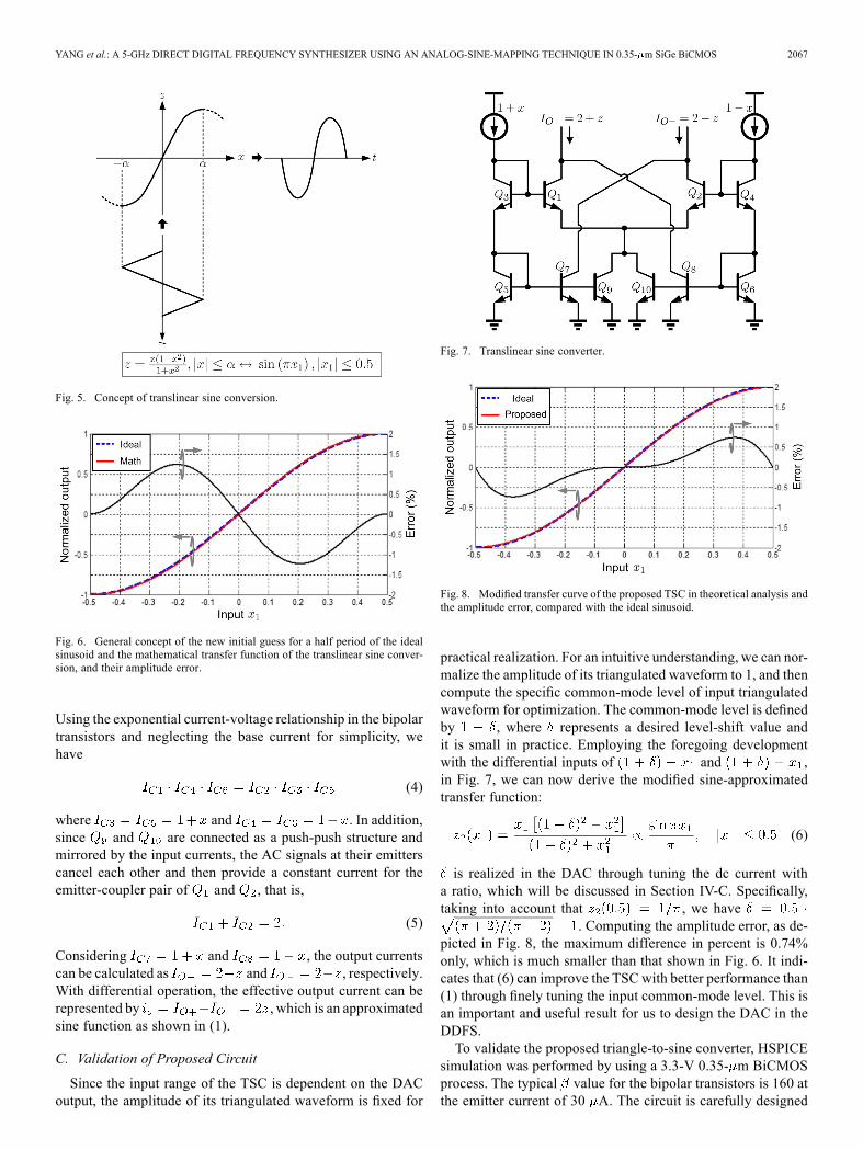
As can be seen, the zero slope of is located at , where. To achieve triangle-to-sine conversion, the
parabolic-approximated function of (1), whose maximum and-axis intersections are the same as that of the sine half-period,is generated for . And the input triangulatedwaveform can be driven by , as shown in Fig. 5. With
Fig. 4. Prior work using a BJT differential pair for triangle-to-sine signal con-version.
for the peak value, we normalize the function asa sine function, that is,
(2)
A complete period of an ideal sinusoid and the employed math-ematical function of (2) are graphed in Fig. 6, which shows thecalculated deviation from an ideal sine wave and the maximumdifference in percent as 1.23%.
B. Translinear Sine-Function Converter
After defining the mathematical description of the translinearsine approximation, the most important point is how it will beelectronically realized. The TSC is realized by the NPN BJTtopology, as shown in Fig. 7. The circuit is connected with nor-malized common inputs and outputs in differential mode. Atranslinear loop exists between base-emitter junctions of tran-sistors to , that is,
(3)
YANG et al.: A 5-GHz DIRECT DIGITAL FREQUENCY SYNTHESIZER USING AN ANALOG-SINE-MAPPING TECHNIQUE IN 0.35- m SiGe BiCMOS 2067
Fig. 5. Concept of translinear sine conversion.
Fig. 6. General concept of the new initial guess for a half period of the idealsinusoid and the mathematical transfer function of the translinear sine conver-sion, and their amplitude error.
Using the exponential current-voltage relationship in the bipolartransistors and neglecting the base current for simplicity, wehave
(4)
where and . In addition,since and are connected as a push-push structure andmirrored by the input currents, the AC signals at their emitterscancel each other and then provide a constant current for theemitter-coupler pair of and , that is,
(5)
Considering and , the output currentscan be calculated as and , respectively.With differential operation, the effective output current can berepresented by , which is an approximatedsine function as shown in (1).
C. Validation of Proposed Circuit
Since the input range of the TSC is dependent on the DACoutput, the amplitude of its triangulated waveform is fixed for
Fig. 7. Translinear sine converter.
Fig. 8. Modified transfer curve of the proposed TSC in theoretical analysis andthe amplitude error, compared with the ideal sinusoid.
practical realization. For an intuitive understanding, we can nor-malize the amplitude of its triangulated waveform to 1, and thencompute the specific common-mode level of input triangulatedwaveform for optimization. The common-mode level is definedby , where represents a desired level-shift value andit is small in practice. Employing the foregoing developmentwith the differential inputs of and ,in Fig. 7, we can now derive the modified sine-approximatedtransfer function:
(6)
is realized in the DAC through tuning the dc current witha ratio, which will be discussed in Section IV-C. Specifically,taking into account that , we have
. Computing the amplitude error, as de-picted in Fig. 8, the maximum difference in percent is 0.74%only, which is much smaller than that shown in Fig. 6. It indi-cates that (6) can improve the TSC with better performance than(1) through finely tuning the input common-mode level. This isan important and useful result for us to design the DAC in theDDFS.To validate the proposed triangle-to-sine converter, HSPICE
simulation was performed by using a 3.3-V 0.35- m BiCMOSprocess. The typical value for the bipolar transistors is 160 atthe emitter current of 30 A. The circuit is carefully designed
2068 IEEE JOURNAL OF SOLID-STATE CIRCUITS, VOL. 46, NO. 9, SEPTEMBER 2011
Fig. 9. Simulated performance of impurity harmonics (including the third andthe fifth harmonics) and total harmonic distortion versus the input frequency.
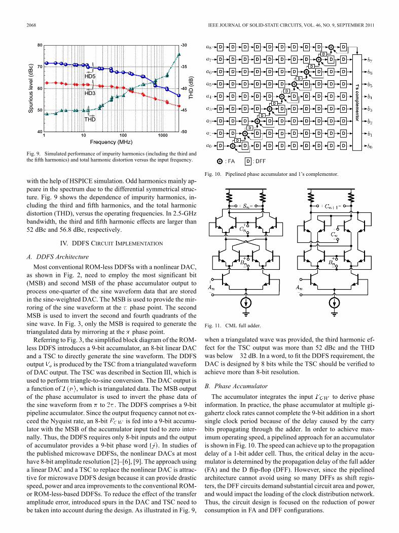
with the help of HSPICE simulation. Odd harmonics mainly ap-peare in the spectrum due to the differential symmetrical struc-ture. Fig. 9 shows the dependence of impurity harmonics, in-cluding the third and fifth harmonics, and the total harmonicdistortion (THD), versus the operating frequencies. In 2.5-GHzbandwidth, the third and fifth harmonic effects are larger than52 dBc and 56.8 dBc, respectively.
IV. DDFS CIRCUIT IMPLEMENTATION
A. DDFS Architecture
Most conventional ROM-less DDFSs with a nonlinear DAC,as shown in Fig. 2, need to employ the most significant bit(MSB) and second MSB of the phase accumulator output toprocess one-quarter of the sine waveform data that are storedin the sine-weighted DAC. The MSB is used to provide the mir-roring of the sine waveform at the phase point. The secondMSB is used to invert the second and fourth quadrants of thesine wave. In Fig. 3, only the MSB is required to generate thetriangulated data by mirroring at the phase point.Referring to Fig. 3, the simplified block diagram of the ROM-
less DDFS introduces a 9-bit accumulator, an 8-bit linear DACand a TSC to directly generate the sine waveform. The DDFSoutput is produced by the TSC from a triangulated waveformof DAC output. The TSC was described in Section III, which isused to perform triangle-to-sine conversion. The DAC output isa function of , which is triangulated data. The MSB outputof the phase accumulator is used to invert the phase data ofthe sine waveform from to . The DDFS comprises a 9-bitpipeline accumulator. Since the output frequency cannot not ex-ceed the Nyquist rate, an 8-bit is fed into a 9-bit accumu-lator with the MSB of the accumulator input tied to zero inter-nally. Thus, the DDFS requires only 8-bit inputs and the outputof accumulator provides a 9-bit phase word . In studies ofthe published microwave DDFSs, the nonlinear DACs at mosthave 8-bit amplitude resolution [2]–[6], [9]. The approach usinga linear DAC and a TSC to replace the nonlinear DAC is attrac-tive for microwave DDFS design because it can provide drasticspeed, power and area improvements to the conventional ROM-or ROM-less-based DDFSs. To reduce the effect of the transferamplitude error, introduced spurs in the DAC and TSC need tobe taken into account during the design. As illustrated in Fig. 9,
Fig. 10. Pipelined phase accumulator and 1’s complementor.
Fig. 11. CML full adder.
when a triangulated wave was provided, the third harmonic ef-fect for the TSC output was more than 52 dBc and the THDwas below 32 dB. In a word, to fit the DDFS requirement, theDAC is designed by 8 bits while the TSC should be verified toachieve more than 8-bit resolution.
B. Phase Accumulator
The accumulator integrates the input to derive phaseinformation. In practice, the phase accumulator at multiple gi-gahertz clock rates cannot complete the 9-bit addition in a shortsingle clock period because of the delay caused by the carrybits propagating through the adder. In order to achieve max-imum operating speed, a pipelined approach for an accumulatoris shown in Fig. 10. The speed can achieve up to the propagationdelay of a 1-bit adder cell. Thus, the critical delay in the accu-mulator is determined by the propagation delay of the full adder(FA) and the D flip-flop (DFF). However, since the pipelinedarchitecture cannot avoid using so many DFFs as shift regis-ters, the DFF circuits demand substantial circuit area and power,and would impact the loading of the clock distribution network.Thus, the circuit design is focused on the reduction of powerconsumption in FA and DFF configurations.
YANG et al.: A 5-GHz DIRECT DIGITAL FREQUENCY SYNTHESIZER USING AN ANALOG-SINE-MAPPING TECHNIQUE IN 0.35- m SiGe BiCMOS 2069
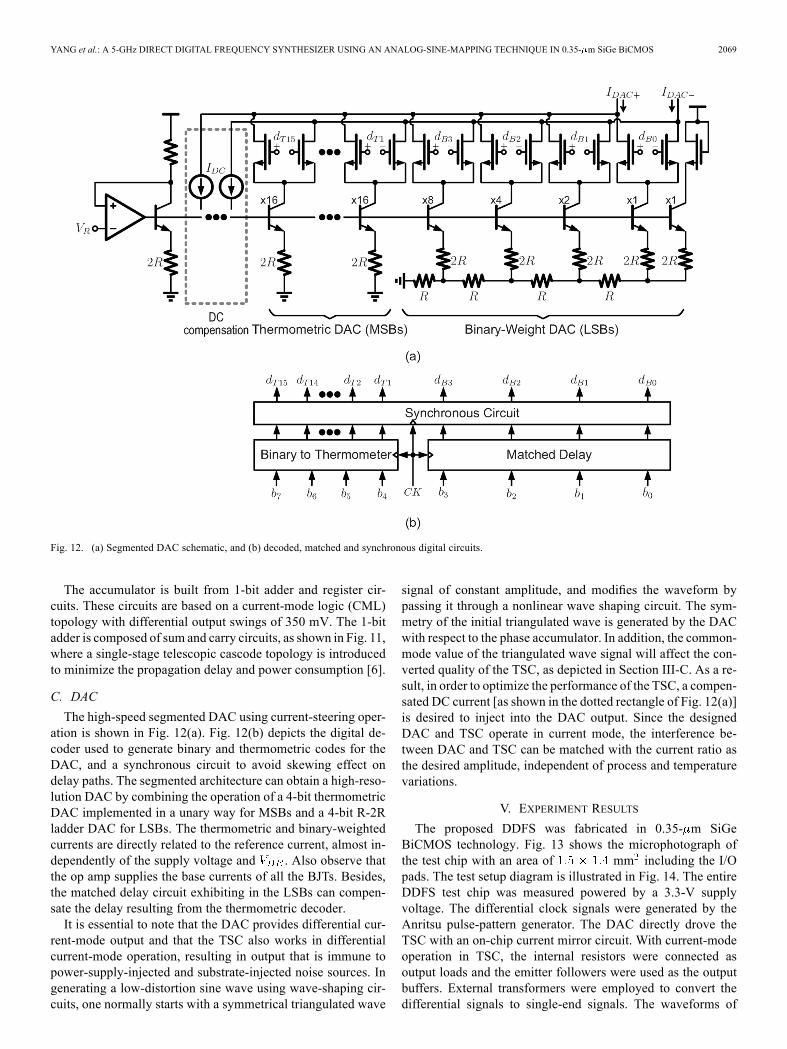
Fig. 12. (a) Segmented DAC schematic, and (b) decoded, matched and synchronous digital circuits.
The accumulator is built from 1-bit adder and register cir-cuits. These circuits are based on a current-mode logic (CML)topology with differential output swings of 350 mV. The 1-bitadder is composed of sum and carry circuits, as shown in Fig. 11,where a single-stage telescopic cascode topology is introducedto minimize the propagation delay and power consumption [6].
C. DAC
The high-speed segmented DAC using current-steering oper-ation is shown in Fig. 12(a). Fig. 12(b) depicts the digital de-coder used to generate binary and thermometric codes for theDAC, and a synchronous circuit to avoid skewing effect ondelay paths. The segmented architecture can obtain a high-reso-lution DAC by combining the operation of a 4-bit thermometricDAC implemented in a unary way for MSBs and a 4-bit R-2Rladder DAC for LSBs. The thermometric and binary-weightedcurrents are directly related to the reference current, almost in-dependently of the supply voltage and . Also observe thatthe op amp supplies the base currents of all the BJTs. Besides,the matched delay circuit exhibiting in the LSBs can compen-sate the delay resulting from the thermometric decoder.It is essential to note that the DAC provides differential cur-
rent-mode output and that the TSC also works in differentialcurrent-mode operation, resulting in output that is immune topower-supply-injected and substrate-injected noise sources. Ingenerating a low-distortion sine wave using wave-shaping cir-cuits, one normally starts with a symmetrical triangulated wave
signal of constant amplitude, and modifies the waveform bypassing it through a nonlinear wave shaping circuit. The sym-metry of the initial triangulated wave is generated by the DACwith respect to the phase accumulator. In addition, the common-mode value of the triangulated wave signal will affect the con-verted quality of the TSC, as depicted in Section III-C. As a re-sult, in order to optimize the performance of the TSC, a compen-sated DC current [as shown in the dotted rectangle of Fig. 12(a)]is desired to inject into the DAC output. Since the designedDAC and TSC operate in current mode, the interference be-tween DAC and TSC can be matched with the current ratio asthe desired amplitude, independent of process and temperaturevariations.
V. EXPERIMENT RESULTS
The proposed DDFS was fabricated in 0.35- m SiGeBiCMOS technology. Fig. 13 shows the microphotograph ofthe test chip with an area of mm including the I/Opads. The test setup diagram is illustrated in Fig. 14. The entireDDFS test chip was measured powered by a 3.3-V supplyvoltage. The differential clock signals were generated by theAnritsu pulse-pattern generator. The DAC directly drove theTSC with an on-chip current mirror circuit. With current-modeoperation in TSC, the internal resistors were connected asoutput loads and the emitter followers were used as the outputbuffers. External transformers were employed to convert thedifferential signals to single-end signals. The waveforms of
2070 IEEE JOURNAL OF SOLID-STATE CIRCUITS, VOL. 46, NO. 9, SEPTEMBER 2011
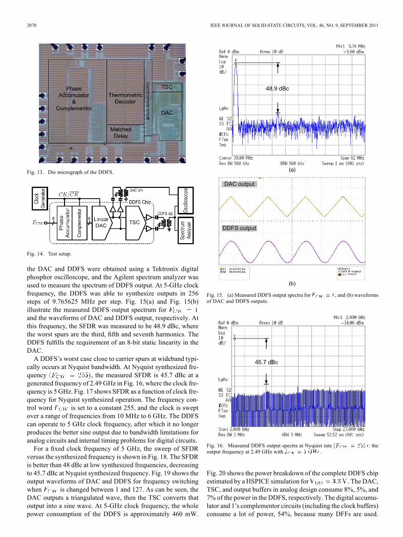
Fig. 13. Die micrograph of the DDFS.
Fig. 14. Test setup.
the DAC and DDFS were obtained using a Tektronix digitalphosphor oscilloscope, and the Agilent spectrum analyzer wasused to measure the spectrum of DDFS output. At 5-GHz clockfrequency, the DDFS was able to synthesize outputs in 256steps of 9.765625 MHz per step. Fig. 15(a) and Fig. 15(b)illustrate the measured DDFS output spectrum forand the waveforms of DAC and DDFS output, respectively. Atthis frequency, the SFDR was measured to be 48.9 dBc, wherethe worst spurs are the third, fifth and seventh harmonics. TheDDFS fulfills the requirement of an 8-bit static linearity in theDAC.A DDFS’s worst case close to carrier spurs at wideband typi-
cally occurs at Nyquist bandwidth. At Nyquist synthesized fre-quency , the measured SFDR is 45.7 dBc at agenerated frequency of 2.49 GHz in Fig. 16, where the clock fre-quency is 5 GHz. Fig. 17 shows SFDR as a function of clock fre-quency for Nyquist synthesized operation. The frequency con-trol word is set to a constant 255, and the clock is sweptover a range of frequencies from 10 MHz to 6 GHz. The DDFScan operate to 5 GHz clock frequency, after which it no longerproduces the better sine output due to bandwidth limitations foranalog circuits and internal timing problems for digital circuits.For a fixed clock frequency of 5 GHz, the sweep of SFDR
versus the synthesized frequency is shown in Fig. 18. The SFDRis better than 48 dBc at low synthesized frequencies, decreasingto 45.7 dBc at Nyquist synthesized frequency. Fig. 19 shows theoutput waveforms of DAC and DDFS for frequency switchingwhen is changed between 1 and 127. As can be seen, theDAC outputs a triangulated wave, then the TSC converts thatoutput into a sine wave. At 5-GHz clock frequency, the wholepower consumption of the DDFS is approximately 460 mW.
Fig. 15. (a) Measured DDFS output spectra for , and (b) waveformsof DAC and DDFS outputs.
Fig. 16. Measured DDFS output spectra at Nyquist rate : theoutput frequency at 2.49 GHz with .
Fig. 20 shows the power breakdown of the complete DDFS chipestimated by a HSPICE simulation for . The DAC,TSC, and output buffers in analog design consume 8%, 5%, and7% of the power in the DDFS, respectively. The digital accumu-lator and 1’s complementor circuits (including the clock buffers)consume a lot of power, 54%, because many DFFs are used.
YANG et al.: A 5-GHz DIRECT DIGITAL FREQUENCY SYNTHESIZER USING AN ANALOG-SINE-MAPPING TECHNIQUE IN 0.35- m SiGe BiCMOS 2071
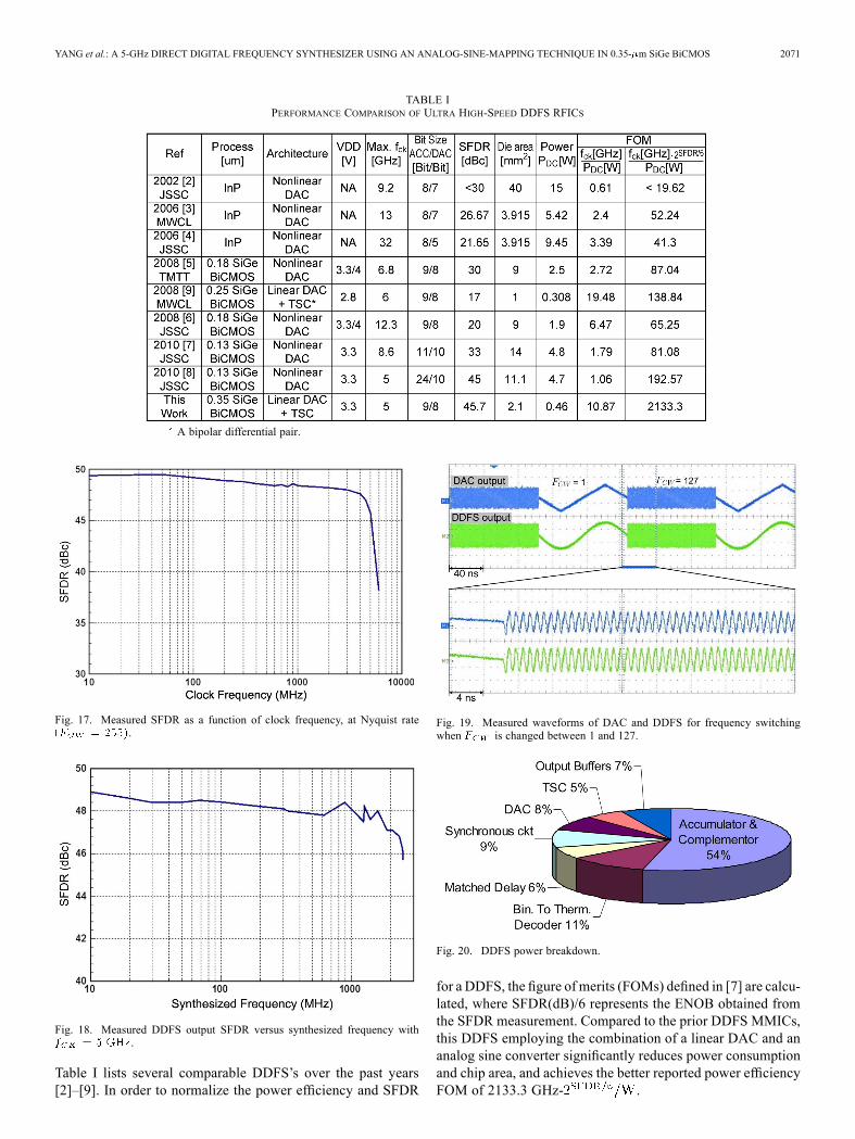
TABLE IPERFORMANCE COMPARISON OF ULTRA HIGH-SPEED DDFS RFICS
A bipolar differential pair.
Fig. 17. Measured SFDR as a function of clock frequency, at Nyquist rate.
Fig. 18. Measured DDFS output SFDR versus synthesized frequency with.
Table I lists several comparable DDFS’s over the past years[2]–[9]. In order to normalize the power efficiency and SFDR
Fig. 19. Measured waveforms of DAC and DDFS for frequency switchingwhen is changed between 1 and 127.
Fig. 20. DDFS power breakdown.
for a DDFS, the figure of merits (FOMs) defined in [7] are calcu-lated, where SFDR(dB)/6 represents the ENOB obtained fromthe SFDR measurement. Compared to the prior DDFS MMICs,this DDFS employing the combination of a linear DAC and ananalog sine converter significantly reduces power consumptionand chip area, and achieves the better reported power efficiencyFOM of 2133.3 GHz- .
2072 IEEE JOURNAL OF SOLID-STATE CIRCUITS, VOL. 46, NO. 9, SEPTEMBER 2011
VI. CONCLUSION
In this paper, a new design technique for ROM-less DDFSusing a linear DAC and an analog TSC is proposed. Comparedto conventional ROM-based DDFSs, it requires significantlyless power, just like the general ROM-less DDFSs using non-linear DAC. The nonlinear DAC requires a sine interpolationalgorithm for phase and amplitude transfer in hybrid digitaland analog domain, leading to a complex and cumbersome de-sign work. Instead of the nonlinear DAC, the combination oflinear DAC and TSC can be designed without any truncation ofdigital control words for a given phase resolution and ampli-tude resolution requirement. Furthermore, the proposed tech-nique will have significant advantages in terms of power dis-sipation and die area over conventional DDFSs for high-fre-quency operation.To demonstrate the proposed technique, the DDFS was im-
plemented with 0.35- m BiCMOS technology. Using the in-herent characteristics of BJTs, the TSC employs a translinearprinciple to fulfill sine function without complex compensatedcircuits. The DDFS covers a bandwidth from dc to 2.5 GHzin steps of 9.765625 MHz. The SFDR is measured to be over48 dBc at low synthesized frequencies and to be 45.7 dBc at2.5 GHz.
ACKNOWLEDGMENT
The authors would like to thank the National Chip Imple-mentation Center (CIC) and the Taiwan Semiconductor Manu-facturing Company (TSMC), Taiwan, for the fabrication of thechip.
REFERENCES
[1] B. Goldberg, Digital Techniques in Frequency Synthesis. New York:McGraw-Hill, 1996.
[2] A. Gutierrez-Aitken, J. Matsui, E. N. Kaneshiro, B. K. Oyama, D.Sawdai, A. K. Oki, and D. C. Streit, “Ultra high speed direct digitalsynthesizer using InP DHBT technology,” IEEE J. Solid-State Circuits,vol. 37, no. 9, pp. 1115–1121, Sep. 2002.
[3] S. E. Turner and D. E. Kotecki, “Direct digital synthesizer with ROM-less architecture at 13-GHz clock frequency in InP DHBT technology,”IEEEMicrow.Wireless Compon. Lett., vol. 16, no. 5, pp. 296–298,May2006.
[4] S. E. Turner and D. E. Kotecki, “Direct digital synthesizer with sine-weighted DAC at 32-GHz clock frequency in InP DHBT technology,”IEEE J. Solid-State Circuits, vol. 41, no. 10, pp. 2284–2290, Oct. 2006.
[5] X. Yu, F. F. Dai, J. D. Irwin, and R. C. Jaeger, “A 9-bit quadraturedirect digital synthesizer implemented in 0.18- m SiGe BiCMOStechnology,” IEEE Trans. Microw. Theory Tech., vol. 56, no. 5, pp.1257–1266, May 2008.
[6] X. Yu, F. F. Dai, J. D. Irwin, and R. C. Jaeger, “A 12 GHz 1.9 Wdirect digital synthesizer MMIC implemented in 0.18- m SiGeBiCMOS technology,” IEEE J. Solid-State Circuits, vol. 43, no. 6, pp.1384–1394, June 2008.
[7] X. Geng, F. F. Dai, J. D. Irwin, and R. C. Jaeger, “A 11-bit 8.6 GHzdirect digital synthesizer MMIC with 10-bit segmented sin-weightedDAC,” IEEE J. Solid-State Circuits, vol. 45, no. 2, pp. 300–313, Feb.2010.
[8] X. Geng, F. F. Dai, J. D. Irwin, and R. C. Jaeger, “24-bit 5.0 GHzdirect digital synthesizer RFIC with direct digital modulations in 0.13m SiGe BiCMOS technology,” IEEE J. Solid-State Circuits, vol. 45,no. 5, pp. 944–954, May 2010.
[9] S. Thuries, E. Tournier, A. Cathelin, S. Godet, and J. Graffeuil, “A6-GHz low-power BiCMOS SiGe:C 0.25 m direct digital synthe-sizer,” IEEEMicrow. Wireless Compon. Lett., vol. 18, no. 1, pp. 46–48,Jan. 2008.
[10] J. Tierney, C.M. Rader, and B. Gold, “A digital frequency synthesizer,”IEEE Trans. Audio Electroacoust., vol. AU-19, pp. 48–57, 1971.
[11] A. Ashrafi and R. Adhami, “Theoretical upperbound of the spurious-free dynamic range in direct digital frequency synthesizers realized bypolynomial interpolation methods,” IEEE Trans. Circuit Syst.—I: Reg-ular Paper, vol. 54, no. 10, pp. 2252–2261, Oct. 2007.
[12] S. Mortezapour and E. K. F. Lee, “Design of low-power ROM-lessdirect digital frequency synthesizer using nonlinear digital-to-analogconverter,” IEEE J. Solid-State Circuits, vol. 34, no. 10, pp.1350–1359, Oct. 1999.
[13] A. N. Mohieldin, A. A. Emira, and E. Sanchez-Sinencio, “A 100-MHz8-mW ROM-less quadrature direct digital frequency synthesizer,”IEEE J. Solid-State Circuits, vol. 37, no. 10, pp. 1235–1243, Oct.2002.
[14] J. Jiang and E. K. F. Lee, “A low-power seqment nonlinear DAC-baseddirect digital frequency synthesizer,” IEEE J. Solid-State Circuits, vol.37, no. 10, pp. 1326–1330, Oct. 2002.
[15] A. McEwan and S. Collins, “Direct digital-frequency synthesis byanalog interpolation,” IEEE Trans. Circuit Systems—II: ExpressBriefs, vol. 53, no. 11, pp. 1294–1298, Nov. 2006.
[16] C. Yang and A. J. Mason, “Fully integrated seven-order fre-quency-range quadrature sinusoid signal generator,” IEEE Trans.Instrum. Measure., vol. 58, no. 10, pp. 3481–3489, Oct. 2009.
[17] W. A. Evans, “Accurate sine-function synthesis,” Electronic Circuitsand Systems, vol. 2, no. 3, pp. 75–78, May 1978.
[18] R. G. Meyer, W. M. C. Sansen, S. Lui, and S. Peeters, “The differentialpair as a triangle-sine wave converter,” IEEE J. Solid-State Circuits,pp. 418–420, June 1976.
[19] J. W. Fattaruso and R. G. Meyer, “Triangle-to-sine wave conversionwith MOS technology,” IEEE J. Solid-State Circuits, vol. sc-20, no. 2,pp. 623–631, Apr. 1985.
[20] B. Gilbert, “Translinear circuits: A proposed classification,” Electron.Lett., vol. 11, pp. 14–16, 1975.
[21] E. Seevinck, Analysis and Synthesis of Translinear Integrated Cir-cuits. : Elsevier, 1988.
Ching-Yuan Yang (S’97–M’01) received the B.S.degree in electrical engineering from the TatungInstitute of Technology, Taipei, Taiwan, R.O.C., in1990, and the M.S. and Ph.D. degrees in electricalengineering from National Taiwan University,Taipei, Taiwan, in 1996 and 2000, respectively.During 2000–2002, he was on the faculty of
Huafan University, Taipei, Taiwan. Since 2002, hehas been on the faculty of National Chung HsingUniversity, Taichung, Taiwan, where he is currentlyan Associate Professor with the Department of
Electrical Engineering. His research interests are in the area of mixed-signalintegrated circuits and systems for high-speed wireline and wireless commu-nications.
Jun-HongWeng (S’06) was born in Yunlin, Taiwan,R.O.C., in 1974. He received the B.S. and M.S. de-grees in electrical engineering from Dayeh Univer-sity, Changhua, Taiwan, in 1998 and 2005, respec-tively. He is currently working toward Ph.D. degreein electrical engineering at Nation Chung Hsing Uni-versity, Taichung, Taiwan. His current research inter-ests include in the area of integrated circuits and sys-tems for high-speed interfaces, wireless communica-tions and low-power ICs.
Hsuan-Yu Chang was born in Yunlin, Taiwan,R.O.C., in 1984. He received the B.S. and M.S. de-grees in electrical engineering from National ChungHsing University in 2006 and 2009, respectively. Heis currently studying for the Ph.D. degree in the De-partment of Electronic Engineering, National ChungHsing University, Taichung, Taiwan. His researchinterests include the analog-to-digital converter andthe digital-to-analog converter.
View publication statsView publication stats