Embed Size (px)
Citation preview

Intel® Quartus® Prime Pro EditionUser GuideDebug Tools
Updated for Intel® Quartus® Prime Design Suite: 18.0
SubscribeSend Feedback
UG-20139 | 2018.07.03Latest document on the web: PDF | HTML
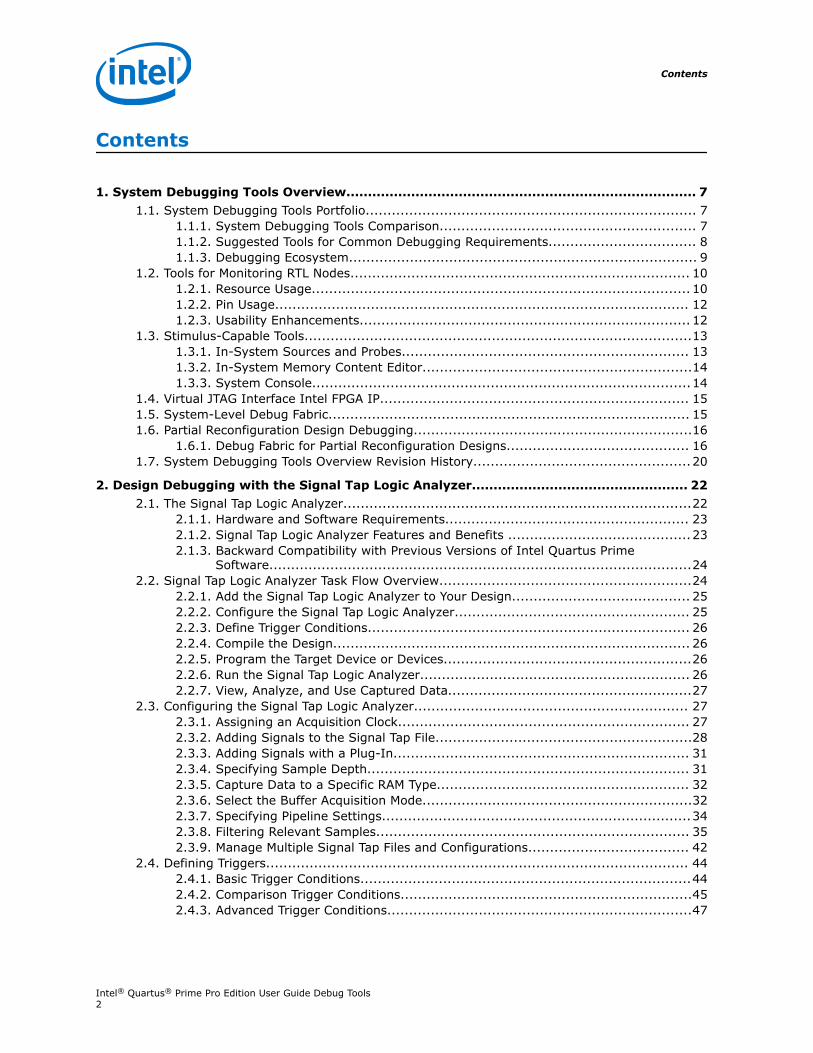
Contents
1. System Debugging Tools Overview................................................................................. 71.1. System Debugging Tools Portfolio............................................................................ 7
1.1.1. System Debugging Tools Comparison........................................................... 71.1.2. Suggested Tools for Common Debugging Requirements.................................. 81.1.3. Debugging Ecosystem................................................................................ 9
1.2. Tools for Monitoring RTL Nodes.............................................................................. 101.2.1. Resource Usage....................................................................................... 101.2.2. Pin Usage............................................................................................... 121.2.3. Usability Enhancements............................................................................ 12
1.3. Stimulus-Capable Tools.........................................................................................131.3.1. In-System Sources and Probes.................................................................. 131.3.2. In-System Memory Content Editor..............................................................141.3.3. System Console.......................................................................................14
1.4. Virtual JTAG Interface Intel FPGA IP....................................................................... 151.5. System-Level Debug Fabric................................................................................... 151.6. Partial Reconfiguration Design Debugging................................................................16
1.6.1. Debug Fabric for Partial Reconfiguration Designs.......................................... 161.7. System Debugging Tools Overview Revision History..................................................20
2. Design Debugging with the Signal Tap Logic Analyzer.................................................. 222.1. The Signal Tap Logic Analyzer................................................................................22
2.1.1. Hardware and Software Requirements........................................................ 232.1.2. Signal Tap Logic Analyzer Features and Benefits ..........................................232.1.3. Backward Compatibility with Previous Versions of Intel Quartus Prime
Software.................................................................................................242.2. Signal Tap Logic Analyzer Task Flow Overview..........................................................24
2.2.1. Add the Signal Tap Logic Analyzer to Your Design......................................... 252.2.2. Configure the Signal Tap Logic Analyzer...................................................... 252.2.3. Define Trigger Conditions.......................................................................... 262.2.4. Compile the Design.................................................................................. 262.2.5. Program the Target Device or Devices.........................................................262.2.6. Run the Signal Tap Logic Analyzer.............................................................. 262.2.7. View, Analyze, and Use Captured Data........................................................27
2.3. Configuring the Signal Tap Logic Analyzer............................................................... 272.3.1. Assigning an Acquisition Clock................................................................... 272.3.2. Adding Signals to the Signal Tap File...........................................................282.3.3. Adding Signals with a Plug-In.................................................................... 312.3.4. Specifying Sample Depth.......................................................................... 312.3.5. Capture Data to a Specific RAM Type.......................................................... 322.3.6. Select the Buffer Acquisition Mode..............................................................322.3.7. Specifying Pipeline Settings.......................................................................342.3.8. Filtering Relevant Samples........................................................................ 352.3.9. Manage Multiple Signal Tap Files and Configurations..................................... 42
2.4. Defining Triggers................................................................................................. 442.4.1. Basic Trigger Conditions............................................................................442.4.2. Comparison Trigger Conditions...................................................................452.4.3. Advanced Trigger Conditions......................................................................47
Contents
Intel® Quartus® Prime Pro Edition User Guide Debug Tools2
2.4.4. Custom Trigger HDL Object....................................................................... 502.4.5. Trigger Condition Flow Control................................................................... 532.4.6. Specify Trigger Position.............................................................................642.4.7. Power-Up Triggers....................................................................................652.4.8. External Triggers......................................................................................67
2.5. Compiling the Design........................................................................................... 672.5.1. Prevent Changes Requiring Recompilation................................................... 672.5.2. Verify Whether You Need to Recompile Your Project...................................... 682.5.3. Incremental Route with Rapid Recompile.....................................................682.5.4. Timing Preservation with the Signal Tap Logic Analyzer................................. 702.5.5. Performance and Resource Considerations...................................................70
2.6. Program the Target Device or Devices.....................................................................712.6.1. Ensure Setting Compatibility Between .stp and .sof Files............................... 72
2.7. Running the Signal Tap Logic Analyzer.................................................................... 722.7.1. Runtime Reconfigurable Options.................................................................732.7.2. Signal Tap Status Messages.......................................................................75
2.8. View, Analyze, and Use Captured Data....................................................................762.8.1. Capturing Data Using Segmented Buffers.................................................... 762.8.2. Differences in Pre-fill Write Behavior Between Different Acquisition Modes....... 782.8.3. Creating Mnemonics for Bit Patterns........................................................... 792.8.4. Automatic Mnemonics with a Plug-In.......................................................... 792.8.5. Locating a Node in the Design................................................................... 802.8.6. Saving Captured Data...............................................................................802.8.7. Exporting Captured Data to Other File Formats............................................ 812.8.8. Creating a Signal Tap List File.................................................................... 81
2.9. Debugging Partial Reconfiguration Designs Using Signal Tap Logic Analyzer................. 812.9.1. Recommendations when Debugging PR Designs........................................... 812.9.2. Setting Up a Partial Reconfiguration Design for Debug...................................822.9.3. Performing Data Acquisition in a PR design..................................................83
2.10. Other Features...................................................................................................842.10.1. Creating Signal Tap File from Design Instances...........................................842.10.2. Using the Signal Tap MATLAB MEX Function to Capture Data........................ 862.10.3. Using Signal Tap in a Lab Environment...................................................... 882.10.4. Remote Debugging Using the Signal Tap Logic Analyzer...............................882.10.5. Using the Signal Tap Logic Analyzer in Devices with Configuration
Bitstream Security................................................................................... 892.10.6. Monitor FPGA Resources Used by the Signal Tap Logic Analyzer.................... 89
2.11. Design Example: Using Signal Tap Logic Analyzers..................................................892.12. Custom Triggering Flow Application Examples........................................................ 90
2.12.1. Design Example 1: Specifying a Custom Trigger Position..............................902.12.2. Design Example 2: Trigger When triggercond1 Occurs Ten Times between
triggercond2 and triggercond3...................................................................912.13. Signal Tap Scripting Support................................................................................91
2.13.1. Signal Tap Command-Line Options............................................................922.13.2. Data Capture from the Command Line...................................................... 92
2.14. Design Debugging with the Signal Tap Logic Analyzer Revision History...................... 93
4. Quick Design Verification with Signal Probe................................................................. 964.1. Debug Flow with Signal Probe and Rapid Recompile..................................................96
4.1.1. Reserve Signal Probe Pins......................................................................... 964.1.2. Compile the Design.................................................................................. 97
Contents
Intel® Quartus® Prime Pro Edition User Guide Debug Tools3
4.1.3. Assign Nodes to Signal Probe Pins.............................................................. 974.1.4. Recompile the Design............................................................................... 974.1.5. Check Connection Table in Fitter Report...................................................... 98
4.2. Quick Design Verification with Signal Probe Revision History...................................... 99
5. In-System Debugging Using External Logic Analyzers................................................ 1005.1. About the Intel Quartus Prime Logic Analyzer Interface........................................... 1005.2. Choosing a Logic Analyzer...................................................................................100
5.2.1. Required Components.............................................................................1015.3. Flow for Using the LAI.........................................................................................102
5.3.1. Defining Parameters for the Logic Analyzer Interface...................................1035.3.2. Mapping the LAI File Pins to Available I/O Pins........................................... 1035.3.3. Mapping Internal Signals to the LAI Banks.................................................1045.3.4. Compiling Your Intel Quartus Prime Project................................................1045.3.5. Programming Your Intel-Supported Device Using the LAI............................. 105
5.4. Controlling the Active Bank During Runtime...........................................................1055.4.1. Acquiring Data on Your Logic Analyzer...................................................... 105
5.5. LAI Core Parameters...........................................................................................1065.6. In-System Debugging Using External Logic Analyzers Revision History...................... 106
6. In-System Modification of Memory and Constants...................................................... 1086.1. IP Cores Supporting ISMCE................................................................................. 1086.2. Debug Flow with the In-System Memory Content Editor.......................................... 1086.3. Enabling Runtime Modification of Instances in the Design........................................ 1096.4. Programming the Device with the In-System Memory Content Editor........................ 1096.5. Loading Memory Instances to the ISMCE...............................................................1106.6. Monitoring Locations in Memory........................................................................... 1116.7. Editing Memory Contents with the Hex Editor Pane................................................. 1136.8. Importing and Exporting Memory Files.................................................................. 1146.9. Access Two or More Devices................................................................................ 1146.10. Scripting Support............................................................................................. 114
6.10.1. The insystem_memory_edit Tcl Package.................................................. 1156.11. In-System Modification of Memory and Constants Revision History..........................115
7. Design Debugging Using In-System Sources and Probes............................................ 1177.1. Hardware and Software Requirements.................................................................. 1197.2. Design Flow Using the In-System Sources and Probes Editor....................................119
7.2.1. Instantiating the In-System Sources and Probes IP Core............................. 1207.2.2. In-System Sources and Probes IP Core Parameters.....................................121
7.3. Compiling the Design..........................................................................................1217.4. Running the In-System Sources and Probes Editor..................................................121
7.4.1. In-System Sources and Probes Editor GUI................................................. 1227.4.2. Programming Your Device With JTAG Chain Configuration............................ 1227.4.3. Instance Manager...................................................................................1227.4.4. In-System Sources and Probes Editor Pane................................................123
7.5. Tcl interface for the In-System Sources and Probes Editor........................................1247.6. Design Example: Dynamic PLL Reconfiguration.......................................................1277.7. Design Debugging Using In-System Sources and Probes Revision History.................. 129
8. Analyzing and Debugging Designs with System Console............................................. 1318.1. Introduction to System Console........................................................................... 1318.2. System Console Debugging Flow.......................................................................... 132
Contents
Intel® Quartus® Prime Pro Edition User Guide Debug Tools4
8.3. IP Cores that Interact with System Console........................................................... 1338.3.1. Services Provided through Debug Agents...................................................133
8.4. Starting System Console..................................................................................... 1348.4.1. Starting System Console from Nios II Command Shell.................................1348.4.2. Starting Stand-Alone System Console....................................................... 1348.4.3. Starting System Console from Platform Designer........................................1348.4.4. Starting System Console from Intel Quartus Prime......................................1358.4.5. Customizing Startup............................................................................... 135
8.5. System Console GUI...........................................................................................1358.5.1. System Explorer Pane.............................................................................136
8.6. System Console Commands.................................................................................1378.7. Running System Console in Command-Line Mode................................................... 1398.8. System Console Services.....................................................................................140
8.8.1. Locating Available Services......................................................................1408.8.2. Opening and Closing Services.................................................................. 1408.8.3. SLD Service...........................................................................................1418.8.4. In-System Sources and Probes Service..................................................... 1428.8.5. Monitor Service......................................................................................1438.8.6. Device Service.......................................................................................1468.8.7. Design Service.......................................................................................1478.8.8. Bytestream Service................................................................................ 1488.8.9. JTAG Debug Service............................................................................... 148
8.9. Working with Toolkits..........................................................................................1498.9.1. Convert your Dashboard Scripts to Toolkit API............................................1508.9.2. Creating a Toolkit Description File.............................................................1508.9.3. Registering a Toolkit............................................................................... 1518.9.4. Launching a Toolkit.................................................................................1518.9.5. Matching Toolkits with IP Cores................................................................ 1518.9.6. Toolkit API.............................................................................................152
8.10. System Console Examples and Tutorials.............................................................. 1898.10.1. Nios II Processor Example..................................................................... 189
8.11. On-Board Intel FPGA Download Cable II Support.................................................. 1918.12. MATLAB and Simulink* in a System Verification Flow ............................................191
8.12.1. Supported MATLAB API Commands......................................................... 1928.12.2. High Level Flow....................................................................................193
8.13. Deprecated Commands..................................................................................... 1938.14. Analyzing and Debugging Designs with System Console Revision History................. 194
9. Debugging Transceiver Links...................................................................................... 1969.1. Device Support.................................................................................................. 1969.2. Channel Manager............................................................................................... 197
9.2.1. Channel Display Modes........................................................................... 1989.3. Transceiver Debugging Flow Walkthrough.............................................................. 1989.4. Modifying the Design to Enable Transceiver Debug..................................................198
9.4.1. Debug Parameters for Transceiver IP Cores................................................1999.5. Programming the Design into an Intel FPGA...........................................................2049.6. Loading the Design in the Transceiver Toolkit......................................................... 2049.7. Linking Hardware Resources................................................................................ 204
9.7.1. Linking One Design to One Device............................................................ 2059.7.2. Linking Two Designs to Two Devices..........................................................2069.7.3. Linking One Design on Two Devices.......................................................... 206
Contents
Intel® Quartus® Prime Pro Edition User Guide Debug Tools5

9.7.4. Linking Designs and Devices on Separate Boards........................................2069.7.5. Verifying Hardware Connections............................................................... 206
9.8. Identifying Transceiver Channels.......................................................................... 2079.8.1. Controlling Transceiver Channels.............................................................. 207
9.9. Creating Transceiver Links...................................................................................2079.10. Running Link Tests............................................................................................208
9.10.1. Running BER Tests................................................................................2089.10.2. Link Optimization Tests......................................................................... 2109.10.3. Running Eye Viewer Tests...................................................................... 210
9.11. Controlling PMA Analog Settings.........................................................................2129.11.1. Intel Arria 10 and Intel Cyclone 10 GX PMA Settings................................. 2129.11.2. Intel Stratix 10 L- and H-Tile PMA Settings...............................................2169.11.3. Intel Stratix 10 E-Tile PMA Settings.........................................................218
9.12. User Interface Settings Reference.......................................................................2219.13. Troubleshooting Common Errors.........................................................................2259.14. Scripting API Reference.....................................................................................225
9.14.1. Transceiver Toolkit Commands................................................................2259.14.2. Data Pattern Generator Commands.........................................................2309.14.3. Data Pattern Checker Commands............................................................231
9.15. Debugging Transceiver Links Revision History.......................................................233
A. Intel Quartus Prime Pro Edition User Guides.............................................................. 236
Contents
Intel® Quartus® Prime Pro Edition User Guide Debug Tools6
1. System Debugging Tools OverviewThis chapter provides a quick overview of the tools available in the Intel® Quartus®
Prime system debugging suite and discusses the criteria for selecting the best tool foryour debug requirements.
1.1. System Debugging Tools Portfolio
The Intel Quartus Prime software provides a portfolio of system debugging tools forreal-time verification of your design.
System debugging tools provide visibility by routing (or “tapping”) signals in yourdesign to debugging logic. The Compiler includes the debugging logic in your designand generates programming files that you download into the FPGA or CPLD foranalysis.
Each tool in the system debugging portfolio uses a combination of available memory,logic, and routing resources to assist in the debugging process. Because differentdesigns have different constraints and requirements, you can choose the tool thatmatches the specific requirements for your design, such as the number of spare pinsavailable or the amount of logic or memory resources remaining in the physicaldevice.
1.1.1. System Debugging Tools Comparison
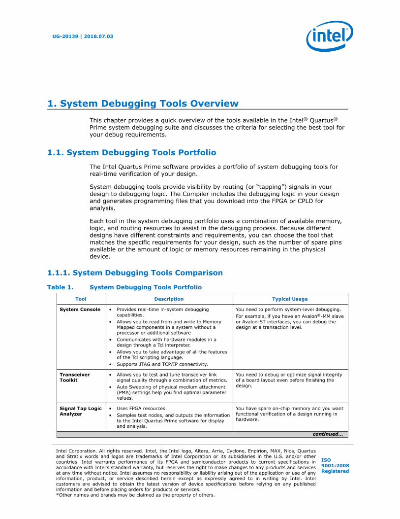
Table 1. System Debugging Tools Portfolio
Tool Description Typical Usage
System Console • Provides real-time in-system debuggingcapabilities.
• Allows you to read from and write to MemoryMapped components in a system without aprocessor or additional software
• Communicates with hardware modules in adesign through a Tcl interpreter.
• Allows you to take advantage of all the featuresof the Tcl scripting language.
• Supports JTAG and TCP/IP connectivity.
You need to perform system-level debugging.For example, if you have an Avalon®-MM slaveor Avalon-ST interfaces, you can debug thedesign at a transaction level.
TransceiverToolkit
• Allows you to test and tune transceiver linksignal quality through a combination of metrics.
• Auto Sweeping of physical medium attachment(PMA) settings help you find optimal parametervalues.
You need to debug or optimize signal integrityof a board layout even before finishing thedesign.
Signal Tap LogicAnalyzer
• Uses FPGA resources.• Samples test nodes, and outputs the information
to the Intel Quartus Prime software for displayand analysis.
You have spare on-chip memory and you wantfunctional verification of a design running inhardware.
continued...
UG-20139 | 2018.07.03
Intel Corporation. All rights reserved. Intel, the Intel logo, Altera, Arria, Cyclone, Enpirion, MAX, Nios, Quartusand Stratix words and logos are trademarks of Intel Corporation or its subsidiaries in the U.S. and/or othercountries. Intel warrants performance of its FPGA and semiconductor products to current specifications inaccordance with Intel's standard warranty, but reserves the right to make changes to any products and servicesat any time without notice. Intel assumes no responsibility or liability arising out of the application or use of anyinformation, product, or service described herein except as expressly agreed to in writing by Intel. Intelcustomers are advised to obtain the latest version of device specifications before relying on any publishedinformation and before placing orders for products or services.*Other names and brands may be claimed as the property of others.
ISO9001:2008Registered
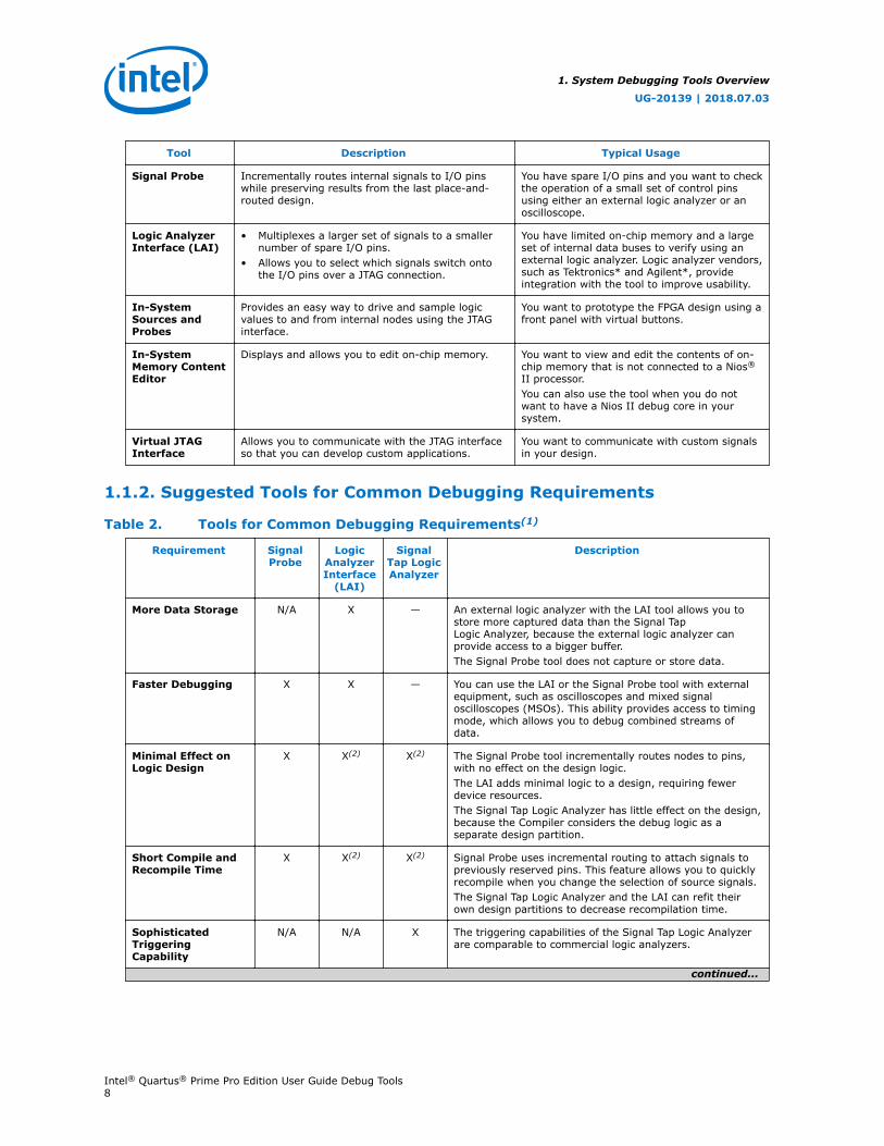
Tool Description Typical Usage
Signal Probe Incrementally routes internal signals to I/O pinswhile preserving results from the last place-and-routed design.
You have spare I/O pins and you want to checkthe operation of a small set of control pinsusing either an external logic analyzer or anoscilloscope.
Logic AnalyzerInterface (LAI)
• Multiplexes a larger set of signals to a smallernumber of spare I/O pins.
• Allows you to select which signals switch ontothe I/O pins over a JTAG connection.
You have limited on-chip memory and a largeset of internal data buses to verify using anexternal logic analyzer. Logic analyzer vendors,such as Tektronics* and Agilent*, provideintegration with the tool to improve usability.
In-SystemSources andProbes
Provides an easy way to drive and sample logicvalues to and from internal nodes using the JTAGinterface.
You want to prototype the FPGA design using afront panel with virtual buttons.
In-SystemMemory ContentEditor
Displays and allows you to edit on-chip memory. You want to view and edit the contents of on-chip memory that is not connected to a Nios®
II processor.You can also use the tool when you do notwant to have a Nios II debug core in yoursystem.
Virtual JTAGInterface
Allows you to communicate with the JTAG interfaceso that you can develop custom applications.
You want to communicate with custom signalsin your design.
1.1.2. Suggested Tools for Common Debugging Requirements
Table 2. Tools for Common Debugging Requirements(1)
Requirement SignalProbe
LogicAnalyzerInterface
(LAI)
SignalTap LogicAnalyzer
Description
More Data Storage N/A X — An external logic analyzer with the LAI tool allows you tostore more captured data than the Signal TapLogic Analyzer, because the external logic analyzer canprovide access to a bigger buffer.The Signal Probe tool does not capture or store data.
Faster Debugging X X — You can use the LAI or the Signal Probe tool with externalequipment, such as oscilloscopes and mixed signaloscilloscopes (MSOs). This ability provides access to timingmode, which allows you to debug combined streams ofdata.
Minimal Effect onLogic Design
X X(2) X(2) The Signal Probe tool incrementally routes nodes to pins,with no effect on the design logic.The LAI adds minimal logic to a design, requiring fewerdevice resources.The Signal Tap Logic Analyzer has little effect on the design,because the Compiler considers the debug logic as aseparate design partition.
Short Compile andRecompile Time
X X(2) X(2) Signal Probe uses incremental routing to attach signals topreviously reserved pins. This feature allows you to quicklyrecompile when you change the selection of source signals.The Signal Tap Logic Analyzer and the LAI can refit theirown design partitions to decrease recompilation time.
SophisticatedTriggeringCapability
N/A N/A X The triggering capabilities of the Signal Tap Logic Analyzerare comparable to commercial logic analyzers.
continued...
1. System Debugging Tools Overview
UG-20139 | 2018.07.03
Intel® Quartus® Prime Pro Edition User Guide Debug Tools8
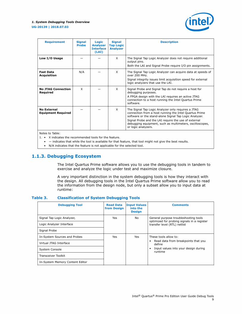
Requirement SignalProbe
LogicAnalyzerInterface
(LAI)
SignalTap LogicAnalyzer
Description
Low I/O Usage — — X The Signal Tap Logic Analyzer does not require additionaloutput pins.Both the LAI and Signal Probe require I/O pin assignments.
Fast DataAcquisition
N/A — X The Signal Tap Logic Analyzer can acquire data at speeds ofover 200 MHz.Signal integrity issues limit acquisition speed for externallogic analyzers that use the LAI.
No JTAG ConnectionRequired
X — X Signal Probe and Signal Tap do not require a host fordebugging purposes.A FPGA design with the LAI requires an active JTAGconnection to a host running the Intel Quartus Primesoftware.
No ExternalEquipment Required
— — X The Signal Tap Logic Analyzer only requires a JTAGconnection from a host running the Intel Quartus Primesoftware or the stand-alone Signal Tap Logic Analyzer.Signal Probe and the LAI require the use of externaldebugging equipment, such as multimeters, oscilloscopes,or logic analyzers.
Notes to Table:1. • X indicates the recommended tools for the feature.
• — indicates that while the tool is available for that feature, that tool might not give the best results.• N/A indicates that the feature is not applicable for the selected tool.
1.1.3. Debugging Ecosystem
The Intel Quartus Prime software allows you to use the debugging tools in tandem toexercise and analyze the logic under test and maximize closure.
A very important distinction in the system debugging tools is how they interact withthe design. All debugging tools in the Intel Quartus Prime software allow you to readthe information from the design node, but only a subset allow you to input data atruntime:
Table 3. Classification of System Debugging Tools
Debugging Tool Read Datafrom Design
Input Valuesinto theDesign
Comments
Signal Tap Logic Analyzer, Yes No General purpose troubleshooting toolsoptimized for probing signals in a registertransfer level (RTL) netlistLogic Analyzer Interface
Signal Probe
In-System Sources and Probes Yes Yes These tools allow to:• Read data from breakpoints that you
define• Input values into your design during
runtime
Virtual JTAG Interface
System Console
Transceiver Toolkit
In-System Memory Content Editor
1. System Debugging Tools Overview
UG-20139 | 2018.07.03
Intel® Quartus® Prime Pro Edition User Guide Debug Tools9
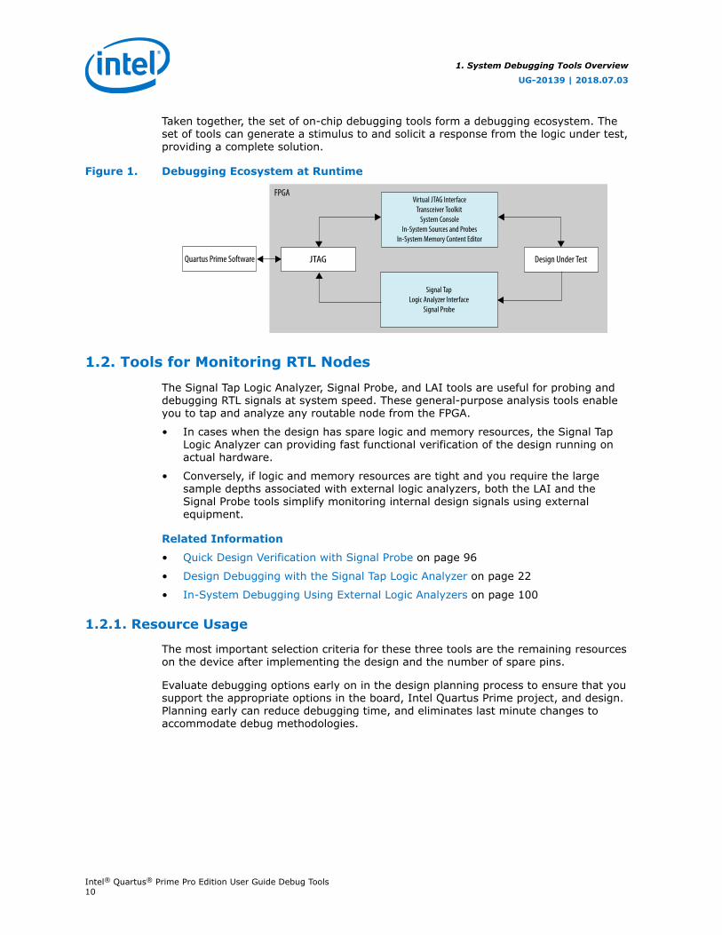
Taken together, the set of on-chip debugging tools form a debugging ecosystem. Theset of tools can generate a stimulus to and solicit a response from the logic under test,providing a complete solution.
Figure 1. Debugging Ecosystem at Runtime
JTAG
FPGA
Quartus Prime Software Design Under Test
Virtual JTAG InterfaceTransceiver Toolkit
System ConsoleIn-System Sources and Probes
In-System Memory Content Editor
Signal TapLogic Analyzer Interface
Signal Probe
1.2. Tools for Monitoring RTL Nodes
The Signal Tap Logic Analyzer, Signal Probe, and LAI tools are useful for probing anddebugging RTL signals at system speed. These general-purpose analysis tools enableyou to tap and analyze any routable node from the FPGA.
• In cases when the design has spare logic and memory resources, the Signal TapLogic Analyzer can providing fast functional verification of the design running onactual hardware.
• Conversely, if logic and memory resources are tight and you require the largesample depths associated with external logic analyzers, both the LAI and theSignal Probe tools simplify monitoring internal design signals using externalequipment.
Related Information
• Quick Design Verification with Signal Probe on page 96
• Design Debugging with the Signal Tap Logic Analyzer on page 22
• In-System Debugging Using External Logic Analyzers on page 100
1.2.1. Resource Usage
The most important selection criteria for these three tools are the remaining resourceson the device after implementing the design and the number of spare pins.
Evaluate debugging options early on in the design planning process to ensure that yousupport the appropriate options in the board, Intel Quartus Prime project, and design.Planning early can reduce debugging time, and eliminates last minute changes toaccommodate debug methodologies.
1. System Debugging Tools Overview
UG-20139 | 2018.07.03
Intel® Quartus® Prime Pro Edition User Guide Debug Tools10
Figure 2. Resource Usage per Debugging Tool
SignalProbe
Logic
Ana
lyzer
Inte
rface
Signal Tap
Logic
Memory
1.2.1.1. Overhead Logic
Any debugging tool that requires a JTAG connection requires SLD infrastructure logicfor communication with the JTAG interface and arbitration between instantiateddebugging modules. This overhead logic uses around 200 logic elements (LEs), a smallfraction of the resources available in any of the supported devices. All availabledebugging modules in your design share the overhead logic. Both the Signal Tap LogicAnalyzer and the LAI use a JTAG connection.
1.2.1.1.1. For Signal Tap Logic Analyzer
The Signal Tap Logic Analyzer requires both logic and memory resources. The numberof logic resources used depends on the number of signals tapped and the complexityof the trigger logic. However, the amount of logic resources that the Signal Tap LogicAnalyzer uses is typically a small percentage of most designs.
A baseline configuration consisting of the SLD arbitration logic and a single node withbasic triggering logic contains approximately 300 to 400 Logic Elements (LEs). Eachadditional node you add to the baseline configuration adds about 11 LEs. Comparedwith logic resources, memory resources are a more important factor to consider foryour design. Memory usage can be significant and depends on how you configure yourSignal Tap Logic Analyzer instance to capture data and the sample depth that yourdesign requires for debugging. For the Signal Tap Logic Analyzer, there is the addedbenefit of requiring no external equipment, as all of the triggering logic and storage ison the chip.
1.2.1.1.2. For Signal Probe
Signal Probe requires very few on-chip resources. Because it requires no JTAGconnection, Signal Probe uses no logic or memory resources. Signal Probe uses onlyrouting resources to route an internal signal to a debugging test point.
1.2.1.1.3. For Logic Analyzer Interface
The LAI requires a small amount of logic to implement the multiplexing functionbetween the signals under test, in addition to the SLD infrastructure logic. Because nodata samples are stored on the chip, the LAI uses no memory resources.
1. System Debugging Tools Overview
UG-20139 | 2018.07.03
Intel® Quartus® Prime Pro Edition User Guide Debug Tools11

1.2.1.2. Resource Estimation
The resource estimation feature for the Signal Tap Logic Analyzer and the LAI allowsyou to quickly judge if enough on-chip resources are available before compiling thetool with your design.
Figure 3. Resource Estimator
1.2.2. Pin Usage
1.2.2.1. For Signal Tap Logic Analyzer
Other than the JTAG test pins, the Signal Tap Logic Analyzer uses no additional pins.All data is buffered using on-chip memory and communicated to the Signal Tap LogicAnalyzer GUI via the JTAG test port.
1.2.2.2. For Signal Probe
The ratio of the number of pins used to the number of signals tapped for the SignalProbe feature is one-to-one. Because this feature can consume free pins quickly, atypical application for this feature is routing control signals to spare pins fordebugging.
1.2.2.3. For Logic Analyzer Interface
The LAI can map up to 256 signals to each debugging pin, depending on availablerouting resources. The JTAG port controls the active signals mapped to the spare I/Opins. With these characteristics, the LAI is ideal for routing data buses to a set of testpins for analysis.
1.2.3. Usability Enhancements
The Signal Tap Logic Analyzer, Signal Probe, and LAI tools can be added to yourexisting design with minimal effects. With the node finder, you can find signals toroute to a debugging module without making any changes to your HDL files. SignalProbe inserts signals directly from your post-fit database. The Signal Tap LogicAnalyzer and LAI support inserting signals from both pre-synthesis and post-fitnetlists.
1.2.3.1. Incremental Routing
Signal Probe uses the incremental routing feature. The incremental routing featureruns only the Fitter stage of the compilation. This leaves your compiled designuntouched, except for the newly routed node or nodes. With Signal Probe, you cansave as much as 90% compile time of a full compilation.
1. System Debugging Tools Overview
UG-20139 | 2018.07.03
Intel® Quartus® Prime Pro Edition User Guide Debug Tools12
1.2.3.2. Automation Via Scripting
As another productivity enhancement, all tools in the on-chip debugging tool setsupport scripting via the quartus_stp Tcl package. For the Signal Tap Logic Analyzerand the LAI, scripting enables user-defined automation for data collection whiledebugging in the lab. The System Console includes a full Tcl interpreter for scripting.
1.2.3.3. Remote Debugging
You can perform remote debugging of a system with the Intel Quartus Prime softwarevia the System Console. This feature allows you to debug equipment deployed in thefield through an existing TCP/IP connection.
• For information about setting up a Nios II system with the System Console toperform remote debugging, refer to Application Note 624
• For information about setting up an Intel FPGA SoC to perform remote debuggingwith the Intel Quartus Prime SLD tools, refer to Application Note 693.
Related Information
• Application Note 624: Debugging with System Console over TCP/IP
• Application Note 693: Remote Debugging over TCP/IP for Intel FPGA SoC
1.3. Stimulus-Capable Tools
The In-System Memory Content Editor, In-System Sources and Probes, and VirtualJTAG interface enable you to use the JTAG interface as a general-purposecommunication port.
Though you can use all three tools to achieve the same results, there are someconsiderations that make one tool easier to use in certain applications:
• The In-System Sources and Probes is ideal for toggling control signals.
• The In-System Memory Content Editor is useful for inputting large sets of testdata.
• Finally, the Virtual JTAG interface is well suited for advanced users who want todevelop custom JTAG solutions.
System Console provides system-level debugging at a transaction level, such as withAvalon-MM slave or Avalon-ST interfaces. You can communicate to a chip throughJTAG and TCP/IP protocols. System Console uses a Tcl interpreter to communicatewith hardware modules that you instantiate into your design.
1.3.1. In-System Sources and Probes
In-System Sources and Probes allow you to read and write to a design by accessingJTAG resources.
You instantiate an Intel FPGA IP into your HDL code. This Intel FPGA IP core containssource ports and probe ports that you connect to signals in your design, and abstractsthe JTAG interface's transaction details.
1. System Debugging Tools Overview
UG-20139 | 2018.07.03
Intel® Quartus® Prime Pro Edition User Guide Debug Tools13
In addition, In-System Sources and Probes provide a GUI that displays source andprobe ports by instance, and allows you to read from probe ports and drive to sourceports. These features make this tool ideal for toggling a set of control signals duringthe debugging process.
Related Information
Design Debugging Using In-System Sources and Probes on page 117
1.3.1.1. Push Button Functionality
During the development phase of a project, you can debug your design using the In-System Sources and Probes GUI instead of push buttons and LEDs. Furthermore, In-System Sources and Probes supports a set of scripting commands for reading andwriting using the Signal Tap logic analyzer. You can also build your own Tk graphicalinterfaces using the Toolkit API. This feature is ideal for building a virtual front panelduring the prototyping phase of the design.
Related Information
• Toolkit API on page 152
• Signal Tap Scripting Support on page 91
1.3.2. In-System Memory Content Editor
The In-System Memory Content Editor allows you to quickly view and modify memorycontent either through a GUI interface or through Tcl scripting commands. The In-System Memory Content Editor works by turning single-port RAM blocks into dual-portRAM blocks. One port is connected to your clock domain and data signals, and theother port is connected to the JTAG clock and data signals for editing or viewing.
Related Information
In-System Modification of Memory and Constants on page 108
1.3.2.1. Generate Test Vectors
Because you can modify a large set of data easily, a useful application for theIn-System Memory Content Editor is to generate test vectors for your design. Forexample, you can instantiate a free memory block, connect the output ports to thelogic under test (using the same clock as your logic under test on the system side),and create the glue logic for the address generation and control of the memory. Atruntime, you can modify the contents of the memory using either a script or theIn-System Memory Content Editor GUI and perform a burst transaction of the datacontents in the modified RAM block synchronous to the logic being tested.
1.3.3. System Console
System Console is a framework that you can launch from the Intel Quartus Primesoftware to start services for performing various debugging tasks. System Consoleprovides you with Tcl scripts and a GUI to access the Platform Designer systemintegration tool to perform low-level hardware debugging of your design, as well asidentify a module by its path, and open and close a connection to a Platform Designermodule. You can access your design at a system level for purposes of loading,unloading, and transferring designs to multiple devices. Also, System Consolesupports the Tk toolkit for building graphical interfaces.
1. System Debugging Tools Overview
UG-20139 | 2018.07.03
Intel® Quartus® Prime Pro Edition User Guide Debug Tools14
Related Information
Analyzing and Debugging Designs with System Console on page 131
1.3.3.1. Test Signal Integrity
System Console also allows you to access commands that allow you to control howyou generate test patterns, as well as verify the accuracy of data generated by testpatterns. You can use JTAG debug commands in System Console to verify thefunctionality and signal integrity of your JTAG chain. You can test clock and resetsignals.
1.3.3.2. Board Bring-Up and Verification
You can use System Console to access programmable logic devices on yourdevelopment board, perform board bring-up, and perform verification. You can alsoaccess software running on a Nios II or Intel FPGA SoC processor, as well as accessmodules that produce or consume a stream of bytes.
1.3.3.3. Test Link Signal Integrity with Transceiver Toolkit
Transceiver Toolkit runs from the System Console framework, and allows you to runautomatic tests of your transceiver links for debugging and optimizing your transceiverdesigns. You can use the Transceiver Toolkit GUI to set up channel links in yourtransceiver devices and change parameters at runtime to measure signal integrity. Forselected devices, the Transceiver Toolkit can also run and display eye contour tests.
1.4. Virtual JTAG Interface Intel FPGA IP
The Virtual JTAG Interface Intel FPGA IP provides the finest level of granularity formanipulating the JTAG resource. This Intel FPGA IP allows you to build your own JTAGscan chain by exposing all of the JTAG control signals and configuring your JTAGInstruction Registers (IRs) and JTAG Data Registers (DRs). During runtime, youcontrol the IR/DR chain through a Tcl API, or with System Console. This feature ismeant for users who have a thorough understanding of the JTAG interface and wantprecise control over the number and type of resources used.
Related Information
• Virtual JTAG (altera_virtual_jtag) IP Core User Guide
• Virtual JTAG Interface (VJI) Intel FPGA IPIn Intel Quartus Prime Help
1.5. System-Level Debug Fabric
During compilation, the Intel Quartus Prime generates the JTAG Hub to allow multipleinstances of debugging tools in a design.
Most Intel FPGA on-chip debugging tools use the JTAG port to control and read-backdata from debugging logic and signals under test. The JTAG Hub manages the sharingof JTAG resources.
Note: For System Console, you explicitly insert debug IP cores into the design to enabledebugging.
1. System Debugging Tools Overview
UG-20139 | 2018.07.03
Intel® Quartus® Prime Pro Edition User Guide Debug Tools15

The JTAG Hub appears in the project's design hierarchy as a partition namedauto_fab_<number>.
1.6. Partial Reconfiguration Design Debugging
The Signal Tap logic analyzer allows you to debug static or PR regions of a design. Ifyou just want to debug the static region, you can use the In-System Sources andProbes Editor, In-System Memory Content Editor, or JTAG Avalon Master Bridge.
Related Information
Debugging Partial Reconfiguration Designs Using Signal Tap Logic Analyzer on page81
1.6.1. Debug Fabric for Partial Reconfiguration Designs
You must prepare the design for PR debug during the early planning stage, to ensurethat you can debug the static as well as PR region.
On designs with Partial Reconfiguration, the Compiler generates centralized debugmanagers—or hubs—for each region (static and PR) that contains system level debugagents. Each hub handles the debug agents in its partition. In the design hierarchy,the hub corresponding to the static region is auto_fab_0.
To connect the hubs on parent and child partitions, you must instantiate one SLD JTAGBridge for each PR region that you want to debug.
Related Information
• Setting Up a Partial Reconfiguration Design for Debug on page 82
• Debugging Partial Reconfiguration Designs Using Signal Tap Logic Analyzer onpage 81
1.6.1.1. SLD JTAG Bridge
The SLD JTAG Bridge connects the debug fabric through PR regions. This bridgeconsists of two IP components:
• SLD JTAG Bridge Agent Intel FPGA IP—debug agent that resides in the staticregion.
• SLD JTAG Bridge Host Intel FPGA IP—resides in the PR region. Connects to thePR JTAG hub on one end, and to the SLD JTAG Bridge Agent on the static region.
1. System Debugging Tools Overview
UG-20139 | 2018.07.03
Intel® Quartus® Prime Pro Edition User Guide Debug Tools16

Figure 4. Signals in a SLD JTAG Bridge
SLD JTAG Bridge AgentStatic PR
SLD JTAG Bridge Host
ena
tdo
vir_tdi
tdi
tms
tck SLD HOST INTERFACESLD HOST INTERFACE
SLD AGENT INTERFACE
Manual Instantiation Automatic InstantiationAutomatic Instantiation
Debug LogicHUB
auto_fab_0HUB
auto_fab_n
For each PR region you debug, you must instantiate one SLD JTAG Bridge Agent in thestatic region and one SLD JTAG Bridge Host in the PR region.
Figure 5. Debug Fabric in PR Design with Signal TapThe figure shows in solid outline the entities that you instantiate manually, and in dashed outline the entitiesthat the Compiler instantiates.
Static Region
STP
HUBPR1
STPBridg
e Age
nt
Bridg
e Hos
t
HUB
PR1
STPBridg
e Age
nt
Bridg
e Hos
t
HUBManual Instantiation
Automatic Instantiation
1.6.1.1.1. SLD JTAG Bridge Index
The SLD JTAG Bridge Index uniquely identifies instances of the SLD JTAG Bridgepresent in a design. You can find information regarding the Bridge Index in thesynthesis report.
The Intel Quartus Prime software supports multiple instances of the SLD JTAG Bridgein designs. The Compiler assigns an index number to distinguish each instance. Thebridge index for the root partition is always None.
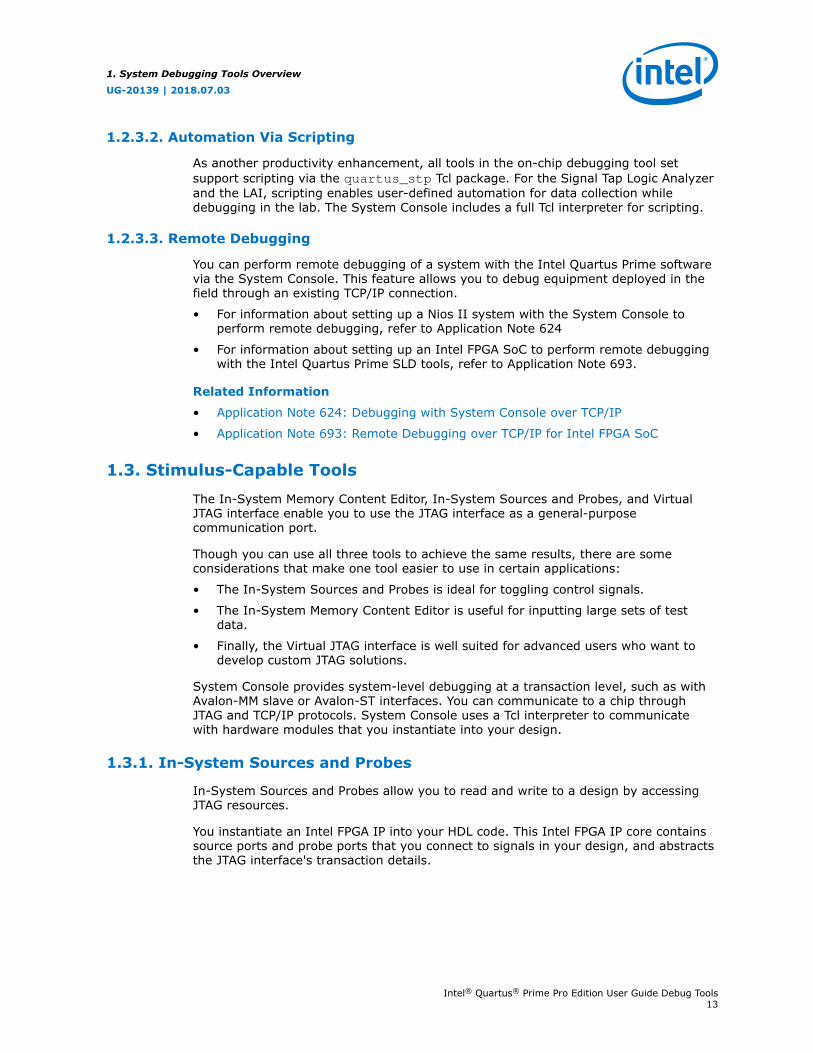
In the synthesis report (<base revision>.syn.rpt), look under “JTAG BridgeAgent Instance Information”.
1. System Debugging Tools Overview
UG-20139 | 2018.07.03
Intel® Quartus® Prime Pro Edition User Guide Debug Tools17
Figure 6. JTAG Bridge Agent Instance Information
1.6.1.1.2. Instantiating the SLD JTAG Bridge Agent
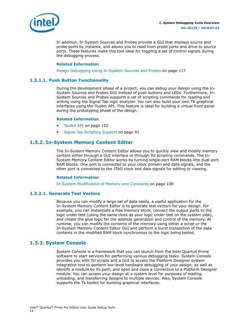
To generate and instantiate the SLD JTAG Bridge Agent Intel FPGA IP:
1. On the IP Catalog (Tools ➤ IP Catalog), type SLD JTAG Bridge Agent.
Figure 7. Find in IP Catalog
2. Double click SLD JTAG Bridge Agent Intel FPGA IP.
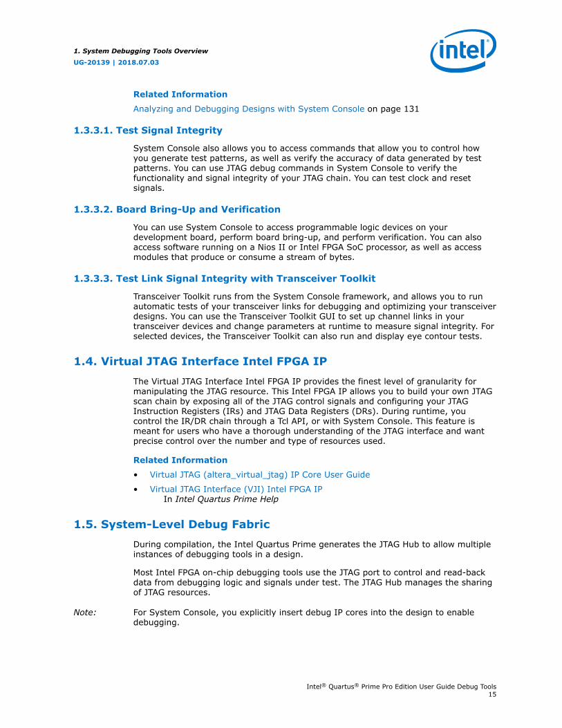
3. In the Create IP Variant dialog box, type a file name, and then click Create.
Figure 8. Create IP Variant Dialog Box
The IP Parameter Editor Pro window shows the IP parameters. In most cases,you do not need to change the default values.
1. System Debugging Tools Overview
UG-20139 | 2018.07.03
Intel® Quartus® Prime Pro Edition User Guide Debug Tools18
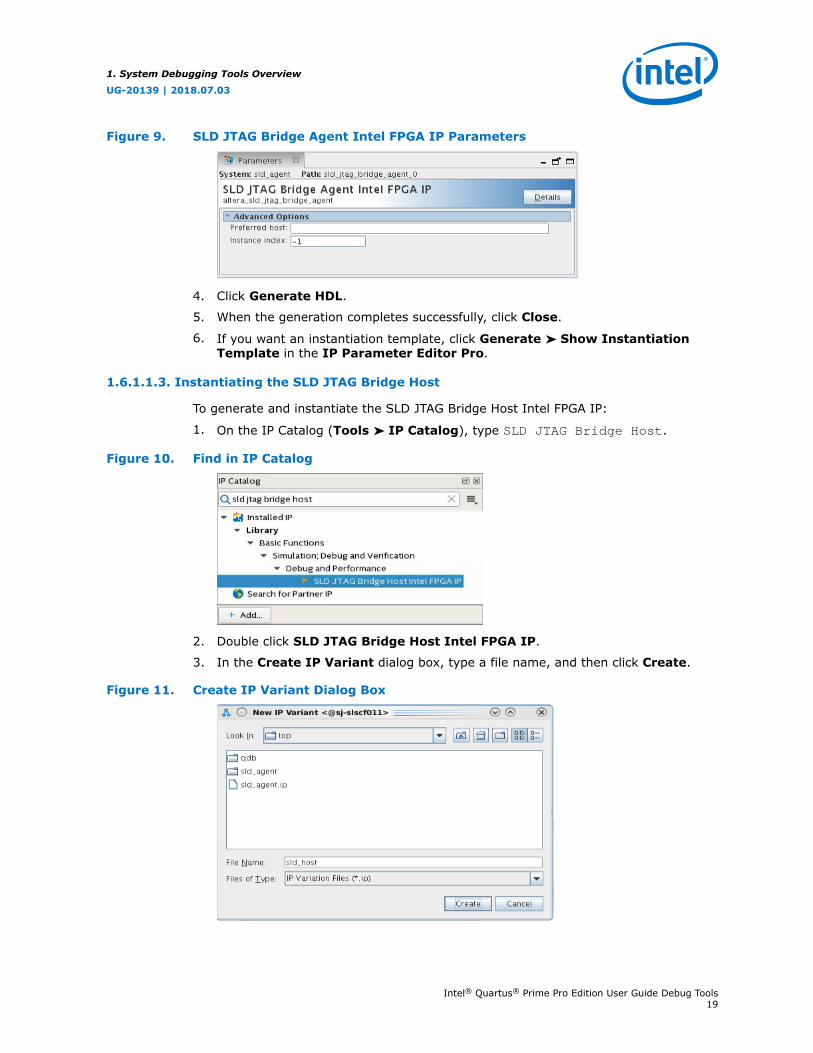
Figure 9. SLD JTAG Bridge Agent Intel FPGA IP Parameters
4. Click Generate HDL.
5. When the generation completes successfully, click Close.
6. If you want an instantiation template, click Generate ➤ Show InstantiationTemplate in the IP Parameter Editor Pro.
1.6.1.1.3. Instantiating the SLD JTAG Bridge Host
To generate and instantiate the SLD JTAG Bridge Host Intel FPGA IP:
1. On the IP Catalog (Tools ➤ IP Catalog), type SLD JTAG Bridge Host.
Figure 10. Find in IP Catalog
2. Double click SLD JTAG Bridge Host Intel FPGA IP.
3. In the Create IP Variant dialog box, type a file name, and then click Create.
Figure 11. Create IP Variant Dialog Box
1. System Debugging Tools Overview
UG-20139 | 2018.07.03
Intel® Quartus® Prime Pro Edition User Guide Debug Tools19
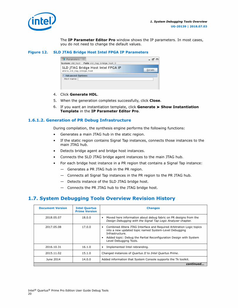
The IP Parameter Editor Pro window shows the IP parameters. In most cases,you do not need to change the default values.
Figure 12. SLD JTAG Bridge Host Intel FPGA IP Parameters
4. Click Generate HDL.
5. When the generation completes successfully, click Close.
6. If you want an instantiation template, click Generate ➤ Show InstantiationTemplate in the IP Parameter Editor Pro.
1.6.1.2. Generation of PR Debug Infrastructure
During compilation, the synthesis engine performs the following functions:
• Generates a main JTAG hub in the static region.
• If the static region contains Signal Tap instances, connects those instances to themain JTAG hub.
• Detects bridge agent and bridge host instances.
• Connects the SLD JTAG bridge agent instances to the main JTAG hub.
• For each bridge host instance in a PR region that contains a Signal Tap instance:
— Generates a PR JTAG hub in the PR region.
— Connects all Signal Tap instances in the PR region to the PR JTAG hub.
— Detects instance of the SLD JTAG bridge host.
— Connects the PR JTAG hub to the JTAG bridge host.
1.7. System Debugging Tools Overview Revision History
Document Version Intel QuartusPrime Version
Changes
2018.05.07 18.0.0 • Moved here information about debug fabric on PR designs from theDesign Debugging with the Signal Tap Logic Analyzer chapter.
2017.05.08 17.0.0 • Combined Altera JTAG Interface and Required Arbitration Logic topicsinto a new updated topic named System-Level DebuggingInfrastructure.
• Added topic: Debug the Partial Reconfiguration Design with SystemLevel Debugging Tools.
2016.10.31 16.1.0 • Implemented Intel rebranding.
2015.11.02 15.1.0 Changed instances of Quartus II to Intel Quartus Prime.
June 2014 14.0.0 Added information that System Console supports the Tk toolkit.
continued...
1. System Debugging Tools Overview
UG-20139 | 2018.07.03
Intel® Quartus® Prime Pro Edition User Guide Debug Tools20

Document Version Intel QuartusPrime Version
Changes
November 2013 13.1.0 Dita conversion. Added link to Remote Debugging over TCP/IP for AlteraSoC Application Note.
June 2012 12.0.0 Maintenance release.
November 2011 10.0.2 Maintenance release. Changed to new document template.
December 2010 10.0.1 Maintenance release. Changed to new document template.
July 2010 10.0.0 Initial release
Related Information
Documentation ArchiveFor previous versions of the Intel Quartus Prime Handbook, search thedocumentation archives.
1. System Debugging Tools Overview
UG-20139 | 2018.07.03
Intel® Quartus® Prime Pro Edition User Guide Debug Tools21
2. Design Debugging with the Signal Tap Logic Analyzer
2.1. The Signal Tap Logic Analyzer
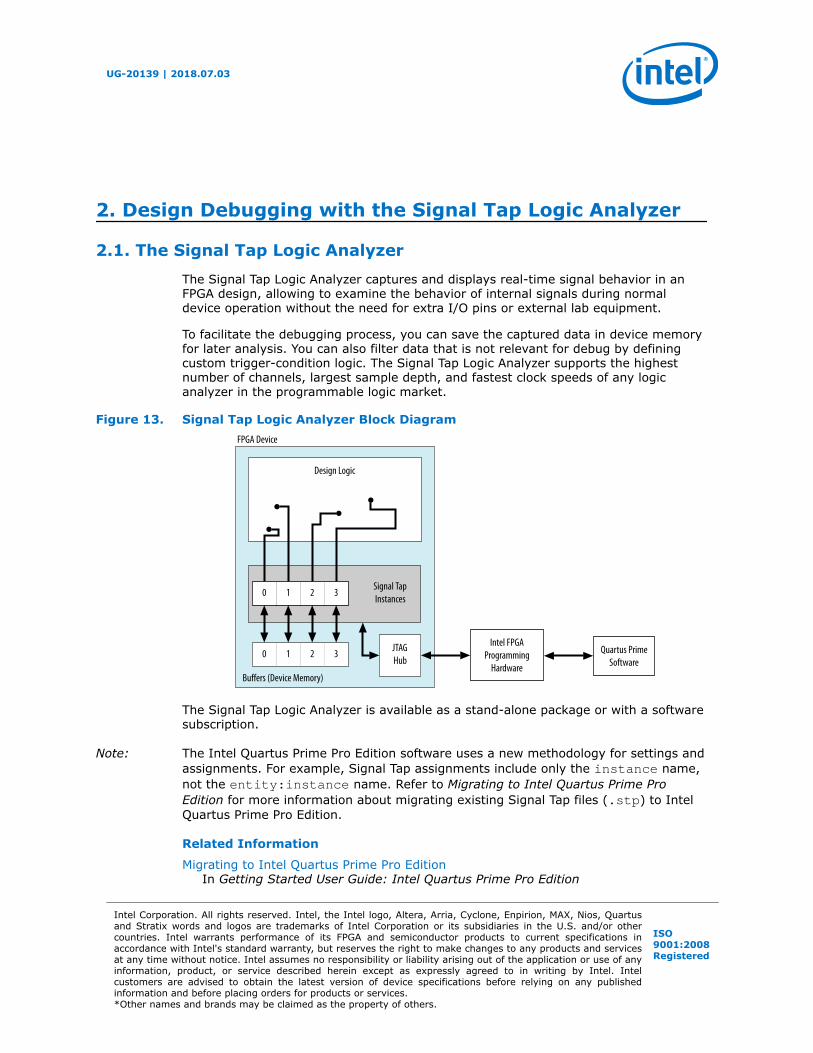
The Signal Tap Logic Analyzer captures and displays real-time signal behavior in anFPGA design, allowing to examine the behavior of internal signals during normaldevice operation without the need for extra I/O pins or external lab equipment.
To facilitate the debugging process, you can save the captured data in device memoryfor later analysis. You can also filter data that is not relevant for debug by definingcustom trigger-condition logic. The Signal Tap Logic Analyzer supports the highestnumber of channels, largest sample depth, and fastest clock speeds of any logicanalyzer in the programmable logic market.
Figure 13. Signal Tap Logic Analyzer Block Diagram
Design Logic
1 2 30
1 2 30
Signal TapInstances
Intel FPGAProgramming
Hardware
Quartus PrimeSoftware
Buffers (Device Memory)
FPGA Device
JTAGHub
The Signal Tap Logic Analyzer is available as a stand-alone package or with a softwaresubscription.
Note: The Intel Quartus Prime Pro Edition software uses a new methodology for settings andassignments. For example, Signal Tap assignments include only the instance name,not the entity:instance name. Refer to Migrating to Intel Quartus Prime ProEdition for more information about migrating existing Signal Tap files (.stp) to IntelQuartus Prime Pro Edition.
Related Information
Migrating to Intel Quartus Prime Pro EditionIn Getting Started User Guide: Intel Quartus Prime Pro Edition
UG-20139 | 2018.07.03
Intel Corporation. All rights reserved. Intel, the Intel logo, Altera, Arria, Cyclone, Enpirion, MAX, Nios, Quartusand Stratix words and logos are trademarks of Intel Corporation or its subsidiaries in the U.S. and/or othercountries. Intel warrants performance of its FPGA and semiconductor products to current specifications inaccordance with Intel's standard warranty, but reserves the right to make changes to any products and servicesat any time without notice. Intel assumes no responsibility or liability arising out of the application or use of anyinformation, product, or service described herein except as expressly agreed to in writing by Intel. Intelcustomers are advised to obtain the latest version of device specifications before relying on any publishedinformation and before placing orders for products or services.*Other names and brands may be claimed as the property of others.
ISO9001:2008Registered
2.1.1. Hardware and Software Requirements
You need the following hardware and software to perform logic analysis with theSignal Tap Logic Analyzer:
• Signal Tap Logic Analyzer
The following software includes the Signal Tap Logic Analyzer:
— Intel Quartus Prime Design Software
— Intel Quartus Prime Lite Edition
Alternatively, use the Signal Tap Logic Analyzer standalone software andstandalone Programmer software.
• Download/upload cable
• Intel development kit or your design board with JTAG connection to device undertest
During data acquisition, the memory blocks in the device store the captured data, andthen transfer the data to the logic analyzer over a JTAG communication cable, such as or Intel FPGA Download Cable.
2.1.1.1. Opening the Standalone Signal Tap Logic Analyzer GUI
1. To open a new Signal Tap through the command-line, type:
quartus_stpw <stp_file.stp>
2.1.2. Signal Tap Logic Analyzer Features and Benefits
Feature Benefit
Quick access toolbar Provides single-click operation of commonly-used menu items. Youcan hover over the icons to see tool tips.
Multiple logic analyzers in a single device Allows you to capture data from multiple clock domains in a design atthe same time.
Multiple logic analyzers in multiple devices in asingle JTAG chain
Allows you to capture data simultaneously from multiple devices in aJTAG chain.
Nios II plug-in support Allows you to specify nodes, triggers, and signal mnemonics for IP,such as the Nios II processor.
Up to 10 basic, comparison, or advanced triggerconditions for each analyzer instance
Allows you to send complex data capture commands to the logicanalyzer, providing greater accuracy and problem isolation.
Power-up trigger Captures signal data for triggers that occur after device programming,but before manually starting the logic analyzer.
Custom trigger HDL object You can code your own trigger in Verilog HDL or VHDL and tap specificinstances of modules located anywhere in the hierarchy of yourdesign, without needing to manually route all the necessaryconnections. This simplifies the process of tapping nodes spread outacross your design.
State-based triggering flow Enables you to organize your triggering conditions to precisely definewhat your logic analyzer captures.
Incremental route with rapid recompile Allows you to manually allocate trigger input, data input, storagequalifier input, and node count, and perform a full compilation toinclude the Signal Tap Logic Analyzer in your design. Then, you can
continued...
2. Design Debugging with the Signal Tap Logic Analyzer
UG-20139 | 2018.07.03
Intel® Quartus® Prime Pro Edition User Guide Debug Tools23

Feature Benefit
selectively connect, disconnect, and swap to different nodes in yourdesign. Use Rapid Recompile to perform incremental routing and gaina 2-4x speedup over the initial full compilation.
Flexible buffer acquisition modes The buffer acquisition control allows you to precisely control the datathat is written into the acquisition buffer. Both segmented buffers andnon-segmented buffers with storage qualification allow you to discarddata samples that are not relevant to the debugging of your design.
MATLAB* integration with included MEX function Collects the data the Signal Tap Logic Analyzer captures into aMATLAB integer matrix.
Up to 2,048 channels per logic analyzer instance Samples many signals and wide bus structures.
Up to 128K samples per instance Captures a large sample set for each channel.
Fast clock frequencies Synchronous sampling of data nodes using the same clock tree drivingthe logic under test.
Resource usage estimator Provides an estimate of logic and memory device resources that theSignal Tap Logic Analyzer configurations use.
No additional cost Intel Quartus Prime subscription and the Intel Quartus Prime LiteEdition include the Signal Tap Logic Analyzer.
Compatibility with other on-chip debuggingutilities
You can use the Signal Tap Logic Analyzer in tandem with any JTAG-based on-chip debugging tool, such as an In-System Memory Contenteditor, allowing you to change signal values in real-time while you arerunning an analysis with the Signal Tap Logic Analyzer.
Floating-Point Display Format To enable, click Edit ➤ Bus Display Format ➤ Floating-pointSupports:• Single-precision floating-point format IEEE754 Single (32-bit).• Double-precision floating-point format IEEE754 Double (64-bit).
Related Information
System Debugging Tools Overview on page 7
2.1.3. Backward Compatibility with Previous Versions of Intel QuartusPrime Software
When you open an .stp file created in a previous version of Intel Quartus Primesoftware in a newer version of the software, the .stp file cannot be opened in aprevious version of the Intel Quartus Prime software.
If you have a Intel Quartus Prime project file from a previous version of the software,you may have to update the .stp configuration file to recompile the project. You canupdate the configuration file by opening the Signal Tap Logic Analyzer. If you need toupdate your configuration, a prompt appears asking if you want to update the .stp tomatch the current version of the Intel Quartus Prime software.
2.2. Signal Tap Logic Analyzer Task Flow Overview
To use the Signal Tap Logic Analyzer to debug your design, you perform a number oftasks to add, configure, and run the logic analyzer.
2. Design Debugging with the Signal Tap Logic Analyzer
UG-20139 | 2018.07.03
Intel® Quartus® Prime Pro Edition User Guide Debug Tools24
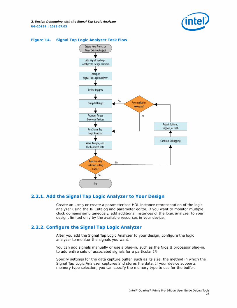
Figure 14. Signal Tap Logic Analyzer Task Flow
End
Yes
NoFunctionalitySatisfied or Bug
Fixed?
Add Signal Tap Logic Analyzer to Design Instance
ConfigureSignal Tap Logic Analyzer
Program TargetDevice or Devices
View, Analyze, andUse Captured Data
Define Triggers
Run Signal Tap Logic Analyzer
Adjust Options, Triggers, or Both
Continue Debugging
RecompilationNecessary?
Yes
Create New Project orOpen Existing Project
NoCompile Design
No
2.2.1. Add the Signal Tap Logic Analyzer to Your Design
Create an .stp or create a parameterized HDL instance representation of the logicanalyzer using the IP Catalog and parameter editor. If you want to monitor multipleclock domains simultaneously, add additional instances of the logic analyzer to yourdesign, limited only by the available resources in your device.
2.2.2. Configure the Signal Tap Logic Analyzer
After you add the Signal Tap Logic Analyzer to your design, configure the logicanalyzer to monitor the signals you want.
You can add signals manually or use a plug-in, such as the Nios II processor plug-in,to add entire sets of associated signals for a particular IP.
Specify settings for the data capture buffer, such as its size, the method in which theSignal Tap Logic Analyzer captures and stores the data. If your device supportsmemory type selection, you can specify the memory type to use for the buffer.
2. Design Debugging with the Signal Tap Logic Analyzer
UG-20139 | 2018.07.03
Intel® Quartus® Prime Pro Edition User Guide Debug Tools25

Related Information
Configuring the Signal Tap Logic Analyzer on page 27
2.2.3. Define Trigger Conditions
By default, the Signal Tap Logic Analyzer captures data continuously while the logicanalyzer is running. To capture and store specific signal data you can set up triggersthat specify conditions to start or stop capturing data.
The Signal Tap Logic Analyzer allows you to define trigger conditions that range fromvery simple, such as the rising edge of a single signal, to very complex, involvinggroups of signals, extra logic, and multiple conditions. Power-Up Triggers allow you tocapture data from trigger events occurring immediately after the device enters user-mode after configuration.
Related Information
Defining Triggers on page 44
2.2.4. Compile the Design
Once you configure the .stp file and define trigger conditions, compile your projectincluding the logic analyzer in your design.
Related Information
Compiling the Design on page 67
2.2.5. Program the Target Device or Devices
When you debug a design with the Signal Tap Logic Analyzer, you can program atarget device directly from the .stp without using the Intel Quartus PrimeProgrammer. You can also program multiple devices with different designs andsimultaneously debug them.
Related Information
• Program the Target Device or Devices on page 71
• Manage Multiple Signal Tap Files and Configurations on page 42
2.2.6. Run the Signal Tap Logic Analyzer
In normal device operation, you control the logic analyzer through the JTAGconnection, specifying when to start looking for trigger conditions to begin capturingdata. With Runtime or Power-Up Triggers, read and transfer the captured data fromthe on-chip buffer to the .stp for analysis.
Related Information
Running the Signal Tap Logic Analyzer on page 72
2. Design Debugging with the Signal Tap Logic Analyzer
UG-20139 | 2018.07.03
Intel® Quartus® Prime Pro Edition User Guide Debug Tools26
2.2.7. View, Analyze, and Use Captured Data
The data you capture and read into the .stp file is available for analysis anddebugging. You can save the data for later analysis, or convert the data to otherformats for sharing and further study.
• To simplify reading and interpreting the signal data you capture, set up mnemonictables, either manually or with a plug-in.
• To speed up debugging, use the Locate feature in the Signal Tap node list tofind the locations of problem nodes in other tools in the Intel Quartus Primesoftware.
Related Information
View, Analyze, and Use Captured Data on page 76
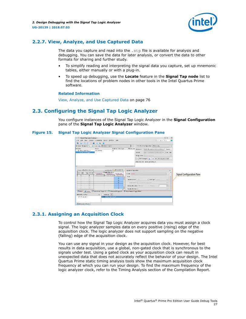
2.3. Configuring the Signal Tap Logic Analyzer
You configure instances of the Signal Tap Logic Analyzer in the Signal Configurationpane of the Signal Tap Logic Analyzer window.
Figure 15. Signal Tap Logic Analyzer Signal Configuration Pane
Signal Configuration Pane
2.3.1. Assigning an Acquisition Clock
To control how the Signal Tap Logic Analyzer acquires data you must assign a clocksignal. The logic analyzer samples data on every positive (rising) edge of theacquisition clock. The logic analyzer does not support sampling on the negative(falling) edge of the acquisition clock.
You can use any signal in your design as the acquisition clock. However, for bestresults in data acquisition, use a global, non-gated clock that is synchronous to thesignals under test. Using a gated clock as your acquisition clock can result inunexpected data that does not accurately reflect the behavior of your design. The IntelQuartus Prime static timing analysis tools show the maximum acquisition clockfrequency at which you can run your design. To find the maximum frequency of thelogic analyzer clock, refer to the Timing Analysis section of the Compilation Report.
2. Design Debugging with the Signal Tap Logic Analyzer
UG-20139 | 2018.07.03
Intel® Quartus® Prime Pro Edition User Guide Debug Tools27
Caution: Be careful when using a recovered clock from a transceiver as an acquisition clock forthe Signal Tap Logic Analyzer. A recovered clock can cause incorrect or unexpectedbehavior, particularly when the transceiver recovered clock is the acquisition clock withthe power-up trigger feature.
If you do not assign an acquisition clock in the Signal Tap Logic Analyzer Editor, IntelQuartus Prime software automatically creates a clock pin calledauto_stp_external_clk. You must make a pin assignment to this pin, and makesure that a clock signal in your design drives the acquisition clock.
Related Information
• Adding Signals with a Plug-In on page 31
• Managing Device I/O PinsIn Design Constraints User Guide: Intel Quartus Prime Pro Edition
2.3.2. Adding Signals to the Signal Tap File
Add the signals that you want to monitor to the .stp node list. You can also selectsignals to define triggers. You can assign the following two signal types:
• Pre-synthesis—These signals exist after design elaboration, but before anysynthesis optimizations are done. This set of signals must reflect your RegisterTransfer Level (RTL) signals.
• Post-fitting—These signals exist after physical synthesis optimizations and place-and-route.
Intel Quartus Prime software does not limit the number of signals available formonitoring in the Signal Tap window waveform display. However, the number ofchannels available is directly proportional to the number of logic elements (LEs) oradaptive logic modules (ALMs) in the device. Therefore, there is a physical restrictionon the number of channels that are available for monitoring. Signals shown in bluetext are post-fit node names. Signals shown in black text are pre-synthesis nodenames.
Note: The Intel Quartus Prime Pro Edition software uses only the instance name, and not theentity name, in the form of:
a|b|c
not a_entity:a|b_entity:b|c_entity:c
After successful Analysis and Elaboration, invalid signals appear in red. Unless you arecertain that these signals are valid, remove them from the .stp file for correctoperation. The Signal Tap Status Indicator also indicates if an invalid node name existsin the .stp file.
You can tap signals if a routing resource (row or column interconnects) exists to routethe connection to the Signal Tap instance. For example, you cannot tap signals thatexist in the I/O element (IOE), because there are no direct routing resources from thesignal in an IOE to a core logic element. For input pins, you can tap the signal that isdriving a logic array block (LAB) from an IOE, or, for output pins, you can tap thesignal from the LAB that is driving an IOE.
2. Design Debugging with the Signal Tap Logic Analyzer
UG-20139 | 2018.07.03
Intel® Quartus® Prime Pro Edition User Guide Debug Tools28
Related Information
Setup Tab (Signal Tap Logic Analyzer)In Intel Quartus Prime Help
2.3.2.1. About Adding Pre-Synthesis Signals
When you add pre-synthesis signals, make all connections to the Signal Tap LogicAnalyzer before synthesis. The Compiler allocates logic and routing resources to makethe connection as if you changed your design files. For signals driving to and fromIOEs, pre-synthesis signal names coincide with the pin's signal names.
2.3.2.2. About Adding Post-Fit Signals
In the case of post-fit signals, connections that you make to the Signal Tap LogicAnalyzer are the signal names from the actual atoms in your post-fit netlist. You canonly make a connection if the signals are part of the existing post-fit netlist, andexisting routing resources are available from the signal of interest to the Signal TapLogic Analyzer.
In the case of post-fit output signals, tap the COMBOUT or REGOUT signal that drivesthe IOE block. For post-fit input signals, signals driving into the core logic coincidewith the pin's signal name.
Note: Because NOT-gate push back applies to any register that you tap, the signal from theatom may be inverted. You can check this by locating the signal in either the ResourceProperty Editor or the Technology Map Viewer. You can also use the Technology Mapviewer and the Resource Property Editor to find post-fit node names.
Related Information
Design Flow with the Netlist ViewersIn Design Optimization User Guide: Intel Quartus Prime Pro Edition
2.3.2.2.1. Assigning Data Signals Using the Technology Map Viewer
You can use the Technology Map Viewer to add post-fit signal names easily. To do so,launch the Technology Map Viewer (post-fitting) after compilation. When you find thedesired node, copy the node to either the active .stp for your design or a new .stp.
To launch the Technology Map Viewer, click Tools ➤ Netlist Viewers ➤ TechnologyMap Viewer (Post-Fitting) in the Intel Quartus Prime window.
2.3.2.3. Preserving Signals
The Intel Quartus Prime software optimizes the RTL signals during synthesis andplace-and-route. RTL signal names may not appear in the post-fit netlist afteroptimizations. For example, the compilation process can add tildes (~) to nets thatfan-out from a node, making it difficult to decipher which signal nets they actuallyrepresent.
The Intel Quartus Prime software provides synthesis attributes that prevent theCompiler to perform any optimization on the specified signals, allowing them to persistinto the post-fit netlist:
• keep—Prevents removal of combinational signals during optimization.
• preserve—Prevents removal of registers during optimization.
2. Design Debugging with the Signal Tap Logic Analyzer
UG-20139 | 2018.07.03
Intel® Quartus® Prime Pro Edition User Guide Debug Tools29
However, using preserving attributes can increase device resource utilization ordecrease timing performance.
If you are debugging an IP core, such as the Nios II CPU or other encrypted IP, youmight need to preserve nodes from the core to keep available for debugging with theSignal Tap Logic Analyzer. Preserving nodes is often necessary when you use a plug-into add a group of signals for a particular IP.
2.3.2.4. Node List Signal Use Options
When you add a signal to the node list, you can select options that specify how thelogic analyzer uses the signal.
To prevent a signal from triggering the analysis, disable the signal's Trigger Enableoption in the .stp file. This option is useful when you only want to see the signal'scaptured data.
You can turn off the ability to view data for a signal by disabling the Data Enablecolumn in the .stp file. This option is useful when you want to trigger on a signal, buthave no interest in viewing that signal's data.
Related Information
Defining Triggers on page 44
2.3.2.4.1. Disabling and Enabling a Signal Tap Instance
Disable and enable Signal Tap instances in the Instance Manager pane. Physicallyadding or removing instances requires recompilation after disabling and enabling aSignal Tap instance.
2.3.2.5. Untappable Signals
Not all the post-fitting signals in your design are available in the Signal Tap : post-fitting filter in the Node Finder dialog box.
You cannot tap any of the following signal types:
• Post-fit output pins—You cannot tap a post-fit output pin directly. To make anoutput signal visible, tap the register or buffer that drives the output pin. Thisincludes pins defined as bidirectional.
• Signals that are part of a carry chain—You cannot tap the carry out (cout0 orcout1) signal of a logic element. Due to architectural restrictions, the carry outsignal can only feed the carry in of another LE.
• JTAG Signals—You cannot tap the JTAG control (TCK, TDI, TDO, and TMS)signals.
• ALTGXB IP core—You cannot directly tap any ports of an ALTGXB instantiation.
• LVDS—You cannot tap the data output from a serializer/deserializer (SERDES)block.
• DQ, DQS Signals—You cannot directly tap the DQ or DQS signals in a DDR/DDRIIdesign.
2. Design Debugging with the Signal Tap Logic Analyzer
UG-20139 | 2018.07.03
Intel® Quartus® Prime Pro Edition User Guide Debug Tools30

2.3.3. Adding Signals with a Plug-In
Instead of adding individual or grouped signals through the Node Finder, you can usea plug-in to add groups of relevant signals of a particular type of IP. Besides easysignal addition, plug-ins provide features such as pre-designed mnemonic tables,useful for trigger creation and data viewing, as well as the ability to disassemble codein captured data. The Signal Tap Logic Analyzer comes with one plug-in for the Nios IIprocessor.
The Nios II plug-in, for example, creates one mnemonic table in the Setup tab andtwo tables in the Data tab:
• Nios II Instruction (Setup tab)—Capture all the required signals for triggeringon a selected instruction address.
• Nios II Instance Address (Data tab)—Display address of executed instructionsin hexadecimal format or as a programming symbol name if defined in an optionalExecutable and Linking Format (.elf) file.
• Nios II Disassembly (Data tab)—Display disassembled code from thecorresponding address.
To add signals to the .stp file using a plug-in, perform the following steps afterrunning Analysis and Elaboration on your design:
1. To ensure that all the required signals are available, in the Intel Quartus Primesoftware, click Assignments ➤ Settings ➤ Compiler Settings ➤ AdvancedSettings (Synthesis). Turn on Create debugging nodes for IP cores.All the signals included in the plug-in are added to the node list.
2. Right-click the node list. On the Add Nodes with Plug-In submenu, select theplug-in you want to use, such as the included plug-in named Nios II.The Select Hierarchy Level dialog box appears showing the IP hierarchy of yourdesign. If the IP for the selected plug-in does not exist in your design, a messageinforms you that you cannot use the selected plug-in.
3. Select the IP that contains the signals you want to monitor with the plug-in, andclick OK.
— If all the signals in the plug-in are available, a dialog box might appear,depending on the plug-in, where you can specify options for the plug-in.
4. With the Nios II plug-in, you can optionally select an .elf containing programsymbols from your Nios II Integrated Development Environment (IDE) softwaredesign. Specify options for the selected plug-in, and click OK.
Related Information
• Defining Triggers on page 44
• View, Analyze, and Use Captured Data on page 27
2.3.4. Specifying Sample Depth
The Sample depth setting specifies the number of samples the Signal Tap LogicAnalyzer captures and stores, for each signal in the captured data buffer.
To specify the sample depth:
1. Select the desired number in the Sample Depth drop-down menu.
The sample depth ranges from 0 to 128K.
2. Design Debugging with the Signal Tap Logic Analyzer
UG-20139 | 2018.07.03
Intel® Quartus® Prime Pro Edition User Guide Debug Tools31
In cases with limited device memory resources, the design may not be able to compiledue to the selected sample buffer size. Try reducing the sample depth to reduceresource usage.
Related Information
Signal Configuration Pane (View Menu) (Signal Tap Logic Analyzer)In Intel Quartus Prime Help
2.3.5. Capture Data to a Specific RAM Type
You have the option to select the RAM type where the Signal Tap Logic Analyzer storesacquisition data. Once you allocate the Signal Tap Logic Analyzer buffer to a particularRAM block, the entire RAM block becomes a dedicated resource for the logic analyzer.
RAM selection allows you to preserve a specific memory block for your design, andallocate another portion of memory for Signal Tap Logic Analyzer data acquisition.
For example, if your design has an application that requires a large block of memoryresources, such as a large instruction or data cache, you can use MLAB blocks for dataacquisition and leave M20k blocks for the rest of your design.
To specify the RAM type to use for the Signal Tap Logic Analyzer buffer, go to theSignal Configuration pane in the Signal Tap window, and select one Ram typefrom the drop-down menu.
Use this feature only when the acquired data is smaller than the available memory ofthe RAM type that you selected. The amount of data appears in the Signal Tapresource estimator.
Related Information
Signal Configuration Pane (View Menu) (Signal Tap Logic Analyzer)In Intel Quartus Prime Help
2.3.6. Select the Buffer Acquisition Mode
When you specify how the logic analyzer organizes the captured data buffer, you canpotentially reduce the amount of memory that Signal Tap requires for data acquisition.
There are two types of acquisition buffer within the Signal Tap Logic Analyzer—a non-segmented (or circular) buffer and a segmented buffer.
• With a non-segmented buffer, the Signal Tap Logic Analyzer treats entire memoryspace as a single FIFO, continuously filling the buffer until the logic analyzerreaches a defined set of trigger conditions.
• With a segmented buffer, the memory space is split into separate buffers. Eachbuffer acts as a separate FIFO with its own set of trigger conditions, and behavesas a non-segmented buffer. Only a single buffer is active during an acquisition.The Signal Tap Logic Analyzer advances to the next segment after the triggercondition or conditions for the active segment has been reached.
When using a non-segmented buffer, you can use the storage qualification feature todetermine which samples are written into the acquisition buffer. Both the segmentedbuffers and the non-segmented buffer with the storage qualification feature help youmaximize the use of the available memory space.
2. Design Debugging with the Signal Tap Logic Analyzer
UG-20139 | 2018.07.03
Intel® Quartus® Prime Pro Edition User Guide Debug Tools32
Figure 16. Buffer Type Comparison in the Signal Tap Logic AnalyzerThe figure illustrates the differences between the two buffer types.
Newly CapturedData
Oldest Data Removed
Post-Trigger Pre-Trigger Center Trigger
1 1
AllTrigger Level
Segment 1 Segment 2 Segment 3 Segment 4
SegmentTrigger Level
1 1 ... 0 1 1 0 ... 0 1 1 1 ... 0 1 1 0 ... 0 1
0 0 1 0 0 1 0 1
SegmentTrigger Level
SegmentTrigger Level
1
(b) Segmented Buffer
(a) Circular Buffer
Both non-segmented and segmented buffers can use a preset trigger position (Pre-Trigger, Center Trigger, Post-Trigger). Alternatively, you can define a custom triggerposition using the State-Based Triggering tab. Refer to Specify Trigger Position formore details.
Related Information
• Specify Trigger Position on page 64
• Filtering Relevant Samples on page 35
2.3.6.1. Non-Segmented Buffer
The non-segmented buffer is the default buffer type in the Signal Tap Logic Analyzer.
At runtime, the logic analyzer stores data in the buffer until the buffer fills up. Fromthat point on, new data overwrites the oldest data, until a specific trigger eventoccurs. The amount of data the buffer captures after the trigger event depends on theTrigger position setting:
• To capture most data before the trigger occurs, select Post trigger position fromthe list
• To capture most data after the trigger, select Pre trigger position.
• To center the trigger position in the data, select Center trigger position.
Alternatively, use the custom State-based triggering flow to define a custom triggerposition within the capture buffer.
Related Information
Specify Trigger Position on page 64
2.3.6.2. Segmented Buffer
In a segmented buffer, the acquisition memory is split into segments of even size, andyou define a set of trigger conditions for each segment. Each segment acts as a non-segmented buffer. A segmented buffer allows you to debug systems that containrelatively infrequent recurring events.
If you want to have separate trigger conditions for each of the segmented buffers, youmust use the state-based trigger flow. The figure shows an example of a segmentedbuffer system.
2. Design Debugging with the Signal Tap Logic Analyzer
UG-20139 | 2018.07.03
Intel® Quartus® Prime Pro Edition User Guide Debug Tools33
Figure 17. System that Generates Recurring EventsIn this design, you want to ensure that the correct data is written to the SRAM controller by monitoring theRDATA port whenever the address H'0F0F0F0F is sent into the RADDR port.
QDR SRAMController
WADDR[17..0]RADDR[17..0]
WDATA[35..0]RDATA[35..0]
CMD[1..0]
INCLK
A[17..0]Q[17..0]D[17..0]BWSn[1..0]RPSnWPSn
K, Kn
QDRSRAM
Reference Design Top-Level File
Stratix Device
PipelineRegisters
(Optional)
K_FB_OUTK_FB_IN
C, Cn
SRAM Interface Signals
With the buffer acquisition feature. you can monitor multiple read transactions fromthe SRAM device without running the Signal Tap Logic Analyzer again, because yousplit the memory to capture the same event multiple times, without wasting allocatedmemory. The buffer captures as many cycles as the number of segments you defineunder the Data settings in the Signal Configuration pane.
To enable and configure buffer acquisition, select Segmented in the Signal Tap LogicAnalyzer Editor and determine the number of segments to use. In the example in thefigure, selecting sixty-four 64-sample segments allows you to capture 64 read cycles.
2.3.7. Specifying Pipeline Settings
The Pipeline factor setting indicates the number of pipeline registers that the IntelQuartus Prime software can add to boost the fMAX of the Signal Tap Logic Analyzer.
To specify the pipeline factor from the Signal Tap GUI:
• In the Signal Configuration pane, specify a pipeline factor ranging from 0 to 5.The default value is 0.
Note: Setting the pipeline factor does not guarantee an increase in fMAX, as the pipelineregisters may not be in the critical paths.
Note: The Signal Tap Intel FPGA IP is not optimized for the Intel Stratix® 10 architecture.
2.3.7.1. Specifying Pipeline Settings from Platform Designer
The Pipeline factor setting indicates the number of pipeline registers that you canadd to boost the fMAX of the Signal Tap Logic Analyzer.
Note: The Signal Tap Intel FPGA IP is not optimized for the Intel Stratix 10 architecture.
You can specify the pipeline factor in the Signal Configuration pane. The pipelinefactor ranges from 0 to 5, with a default value of 0.
2. Design Debugging with the Signal Tap Logic Analyzer
UG-20139 | 2018.07.03
Intel® Quartus® Prime Pro Edition User Guide Debug Tools34
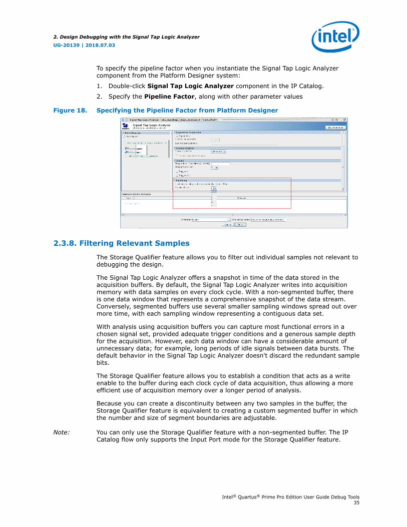
To specify the pipeline factor when you instantiate the Signal Tap Logic Analyzercomponent from the Platform Designer system:
1. Double-click Signal Tap Logic Analyzer component in the IP Catalog.
2. Specify the Pipeline Factor, along with other parameter values
Figure 18. Specifying the Pipeline Factor from Platform Designer
2.3.8. Filtering Relevant Samples
The Storage Qualifier feature allows you to filter out individual samples not relevant todebugging the design.
The Signal Tap Logic Analyzer offers a snapshot in time of the data stored in theacquisition buffers. By default, the Signal Tap Logic Analyzer writes into acquisitionmemory with data samples on every clock cycle. With a non-segmented buffer, thereis one data window that represents a comprehensive snapshot of the data stream.Conversely, segmented buffers use several smaller sampling windows spread out overmore time, with each sampling window representing a contiguous data set.
With analysis using acquisition buffers you can capture most functional errors in achosen signal set, provided adequate trigger conditions and a generous sample depthfor the acquisition. However, each data window can have a considerable amount ofunnecessary data; for example, long periods of idle signals between data bursts. Thedefault behavior in the Signal Tap Logic Analyzer doesn't discard the redundant samplebits.
The Storage Qualifier feature allows you to establish a condition that acts as a writeenable to the buffer during each clock cycle of data acquisition, thus allowing a moreefficient use of acquisition memory over a longer period of analysis.
Because you can create a discontinuity between any two samples in the buffer, theStorage Qualifier feature is equivalent to creating a custom segmented buffer in whichthe number and size of segment boundaries are adjustable.
Note: You can only use the Storage Qualifier feature with a non-segmented buffer. The IPCatalog flow only supports the Input Port mode for the Storage Qualifier feature.
2. Design Debugging with the Signal Tap Logic Analyzer
UG-20139 | 2018.07.03
Intel® Quartus® Prime Pro Edition User Guide Debug Tools35
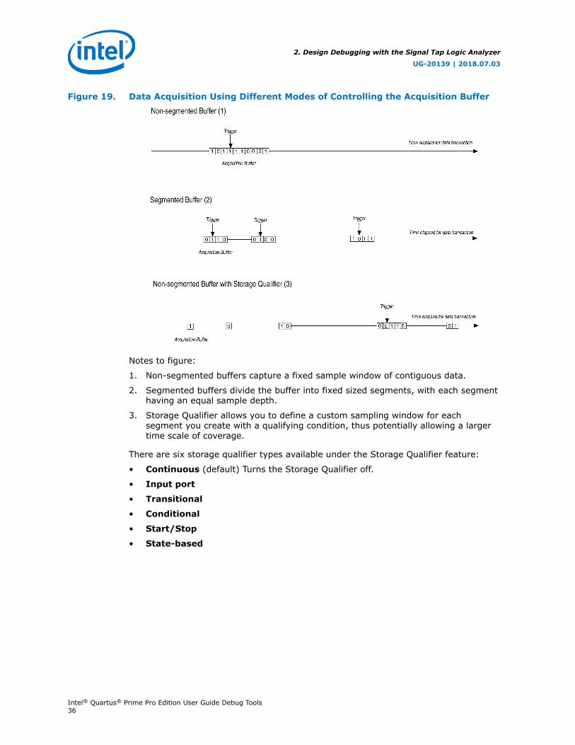
Figure 19. Data Acquisition Using Different Modes of Controlling the Acquisition Buffer
Notes to figure:
1. Non-segmented buffers capture a fixed sample window of contiguous data.
2. Segmented buffers divide the buffer into fixed sized segments, with each segmenthaving an equal sample depth.
3. Storage Qualifier allows you to define a custom sampling window for eachsegment you create with a qualifying condition, thus potentially allowing a largertime scale of coverage.
There are six storage qualifier types available under the Storage Qualifier feature:
• Continuous (default) Turns the Storage Qualifier off.
• Input port
• Transitional
• Conditional
• Start/Stop
• State-based
2. Design Debugging with the Signal Tap Logic Analyzer
UG-20139 | 2018.07.03
Intel® Quartus® Prime Pro Edition User Guide Debug Tools36

Figure 20. Storage Qualifier Settings
Upon the start of an acquisition, the Signal Tap Logic Analyzer examines each clockcycle and writes the data into the buffer based upon the storage qualifier type andcondition. Acquisition stops when a defined set of trigger conditions occur.
The Signal Tap Logic Analyzer evaluates trigger conditions independently of storagequalifier conditions.
Related Information
Define Trigger Conditions on page 26
2.3.8.1. Input Port Mode
When using the Input port mode, the Signal Tap Logic Analyzer takes any signal fromyour design as an input. During acquisition, if the signal is high on the clock edge, theSignal Tap Logic Analyzer stores the data in the buffer. If the signal is low on the clockedge, the Logic Analyzer ignores the data sample. If you don't specify an internalnode, the Logic Analyzer creates and connects a pin to this input port.
If you are creating a Signal Tap Logic Analyzer instance through an .stp file, specifythe storage qualifier signal using the input port field located on the Setup tab. Youmust specify this port for your project to compile.
If you use the parameter editor, the storage qualification input port, if specified,appears in the generated instantiation template. You can then connect this port to asignal in your RTL.
2. Design Debugging with the Signal Tap Logic Analyzer
UG-20139 | 2018.07.03
Intel® Quartus® Prime Pro Edition User Guide Debug Tools37
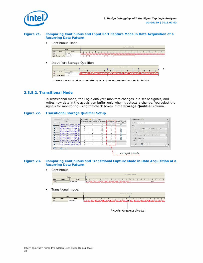
Figure 21. Comparing Continuous and Input Port Capture Mode in Data Acquisition of aRecurring Data Pattern
• Continuous Mode:
• Input Port Storage Qualifier:
2.3.8.2. Transitional Mode
In Transitional mode, the Logic Analyzer monitors changes in a set of signals, andwrites new data in the acquisition buffer only when it detects a change. You select thesignals for monitoring using the check boxes in the Storage Qualifier column.
Figure 22. Transitional Storage Qualifier Setup
Select signals to monitor
Figure 23. Comparing Continuous and Transitional Capture Mode in Data Acquisition of aRecurring Data Pattern
• Continuous:
• Transitional mode:
2. Design Debugging with the Signal Tap Logic Analyzer
UG-20139 | 2018.07.03
Intel® Quartus® Prime Pro Edition User Guide Debug Tools38

2.3.8.3. Conditional Mode
In Conditional mode, the Signal Tap Logic Analyzer determines whether to store asample by evaluating a combinational function of predefined signals within the nodelist. The Signal Tap Logic Analyzer writes into the buffer during the clock cycles inwhich the condition you specify evaluates TRUE.
You can select either Basic AND, Basic OR, Comparison, or Advanced storagequalifier conditions. A Basic AND or Basic OR condition matches each signal to oneof the following:
• Don’t Care
• Low
• High
• Falling Edge
• Rising Edge
• Either Edge
If you specify a Basic AND storage qualifier condition for more than one signal, theSignal Tap Logic Analyzer evaluates the logical AND of the conditions.
You can specify any other combinational or relational operators with the enabled signalset for storage qualification through advanced storage conditions.
You can define storage qualification conditions similar to the manner in which youdefine trigger conditions.
Figure 24. Conditional Storage Qualifier SetupThe figure details the conditional storage qualifier setup in the .stp file.
Storage Enable Storage condition
If the signal is not enabled for storage, it can’t be part of the Storage Qualifier condition
2. Design Debugging with the Signal Tap Logic Analyzer
UG-20139 | 2018.07.03
Intel® Quartus® Prime Pro Edition User Guide Debug Tools39

Figure 25. Comparing Continuous and Conditional Capture Mode in Data Acquisition of aRecurring Data Pattern
The data pattern is the same in both cases.
• Continuous sampling capture mode:
• Conditional sampling capture mode:
Related Information
• Basic Trigger Conditions on page 44
• Comparison Trigger Conditions on page 45
• Advanced Trigger Conditions on page 47
2.3.8.4. Start/Stop Mode
The Start/Stop mode uses two sets of conditions, one to start data capture and one tostop data capture. If the start condition evaluates to TRUE, Signal Tap Logic Analyzerstores the buffer data every clock cycle until the stop condition evaluates to TRUE,which then pauses the data capture. The Logic Analyzer ignores additional startsignals received after the data capture starts. If both start and stop evaluate to TRUEat the same time, the Logic Analyzer captures a single cycle.
Note: You can force a trigger by pressing the Stop button if the buffer fails to fill tocompletion due to a stop condition.
Figure 26. Start/Stop Mode Storage Qualifier SetupStart condition Stop Condition
Storage Qualifier Enabled signals
2. Design Debugging with the Signal Tap Logic Analyzer
UG-20139 | 2018.07.03
Intel® Quartus® Prime Pro Edition User Guide Debug Tools40
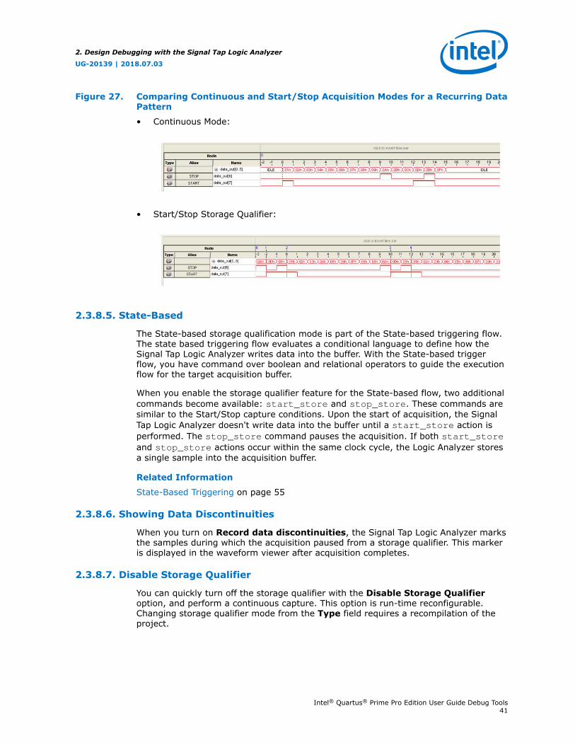
Figure 27. Comparing Continuous and Start/Stop Acquisition Modes for a Recurring DataPattern
• Continuous Mode:
• Start/Stop Storage Qualifier:
2.3.8.5. State-Based
The State-based storage qualification mode is part of the State-based triggering flow.The state based triggering flow evaluates a conditional language to define how theSignal Tap Logic Analyzer writes data into the buffer. With the State-based triggerflow, you have command over boolean and relational operators to guide the executionflow for the target acquisition buffer.
When you enable the storage qualifier feature for the State-based flow, two additionalcommands become available: start_store and stop_store. These commands aresimilar to the Start/Stop capture conditions. Upon the start of acquisition, the SignalTap Logic Analyzer doesn't write data into the buffer until a start_store action isperformed. The stop_store command pauses the acquisition. If both start_storeand stop_store actions occur within the same clock cycle, the Logic Analyzer storesa single sample into the acquisition buffer.
Related Information
State-Based Triggering on page 55
2.3.8.6. Showing Data Discontinuities
When you turn on Record data discontinuities, the Signal Tap Logic Analyzer marksthe samples during which the acquisition paused from a storage qualifier. This markeris displayed in the waveform viewer after acquisition completes.
2.3.8.7. Disable Storage Qualifier
You can quickly turn off the storage qualifier with the Disable Storage Qualifieroption, and perform a continuous capture. This option is run-time reconfigurable.Changing storage qualifier mode from the Type field requires a recompilation of theproject.
2. Design Debugging with the Signal Tap Logic Analyzer
UG-20139 | 2018.07.03
Intel® Quartus® Prime Pro Edition User Guide Debug Tools41

Related Information
Runtime Reconfigurable Options on page 73
2.3.9. Manage Multiple Signal Tap Files and Configurations
You can debug different blocks in your design by grouping related monitoring signals.Likewise, you can use a group of signals to define multiple trigger conditions. Eachcombination of signals, capture settings, and trigger conditions determines a debugconfiguration, and one configuration can have zero or more associated data logs.
Signal Tap Logic Analyzer allows you to save debug configurations in more thanone .stp file. Alternatively, you can embed multiple configurations within thesame .stp file, and use the Data Log as a managing tool.
Note: Each .stp file is associated with a programming (.sof) file. To function correctly, thesettings in the .stp file you use at runtime must match Signal Tap settings inthe .sof file you use to program the device.
Related Information
Ensure Setting Compatibility Between .stp and .sof Files on page 72
2.3.9.1. Data Log Pane
The Data Log pane displays all Signal Tap configurations and data capture resultsstored within a single .stp file.
• To save the current configuration or capture in the Data Log—and .stp file, click
Edit ➤ Save to Data Log. Alternatively, click the Save to Data Log icon atthe top of the Data Log pane.
• To generate a log entry after every data capture, click Edit ➤ Enable Data Log.Alternatively, check the box at the top of the Data Log pane.
The Data Log displays its contents in a tree hierarchy. The active items display adifferent icon.
Table 4. Data Log Items
Item Icon Contains one ormore
Comments
Unselected Selected
Instance Signal Set
Signal Set Trigger The Signal Set changes whenever you add a newsignal to Signal Tap. After a change in the SignalSet, you need to recompile.
Trigger Capture Log A trigger changes when you change any triggercondition. These changes do not requirerecompilation.
Capture Log
The name on each entry displays the wall-clock time when Signal Tap Logic Analyzertriggered, and the time elapsed from start acquisition to trigger activation. You canrename entries so they make sense to you.
2. Design Debugging with the Signal Tap Logic Analyzer
UG-20139 | 2018.07.03
Intel® Quartus® Prime Pro Edition User Guide Debug Tools42

To switch between configurations, double-click an entry in the Data Log. As a result,the Setup tab updates to display the active signal list and trigger conditions.
Example 1. Simple Data Log
On this example, the Data Log displays one instance with three signal setconfigurations.
2.3.9.2. SOF Manager
The SOF Manager is in the JTAG Chain Configuration pane.
With the SOF Manager you can embed multiple SOFs into one .stp file. This actionlets you move the .stp file to a different location, either on the same computer oracross a network, without including the associated .sof separately. To embed a new
SOF in the .stp file, click the Attach SOF File icon .
Figure 28. SOF Manager
Attach SOF File Icon
As you switch between configurations in the Data Log, you can extract the SOF that iscompatible with that configuration.
To download the new SOF to the FPGA, click the Program Device icon in the SOFManager, after ensuring that the configuration of your .stp matches the designprogrammed into the target device.
Related Information
Data Log Pane on page 42
2. Design Debugging with the Signal Tap Logic Analyzer
UG-20139 | 2018.07.03
Intel® Quartus® Prime Pro Edition User Guide Debug Tools43
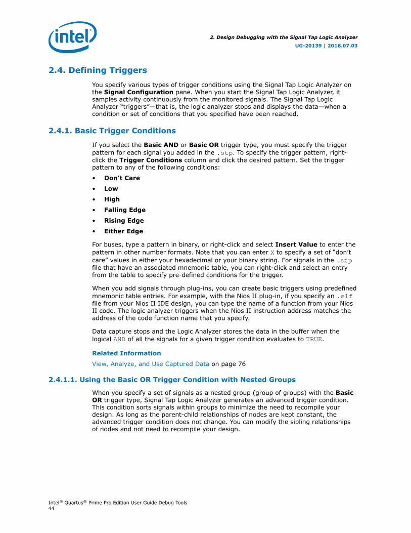
2.4. Defining Triggers
You specify various types of trigger conditions using the Signal Tap Logic Analyzer onthe Signal Configuration pane. When you start the Signal Tap Logic Analyzer, itsamples activity continuously from the monitored signals. The Signal Tap LogicAnalyzer “triggers”—that is, the logic analyzer stops and displays the data—when acondition or set of conditions that you specified have been reached.
2.4.1. Basic Trigger Conditions
If you select the Basic AND or Basic OR trigger type, you must specify the triggerpattern for each signal you added in the .stp. To specify the trigger pattern, right-click the Trigger Conditions column and click the desired pattern. Set the triggerpattern to any of the following conditions:
• Don’t Care
• Low
• High
• Falling Edge
• Rising Edge
• Either Edge
For buses, type a pattern in binary, or right-click and select Insert Value to enter thepattern in other number formats. Note that you can enter X to specify a set of “don’tcare” values in either your hexadecimal or your binary string. For signals in the .stpfile that have an associated mnemonic table, you can right-click and select an entryfrom the table to specify pre-defined conditions for the trigger.
When you add signals through plug-ins, you can create basic triggers using predefinedmnemonic table entries. For example, with the Nios II plug-in, if you specify an .elffile from your Nios II IDE design, you can type the name of a function from your NiosII code. The logic analyzer triggers when the Nios II instruction address matches theaddress of the code function name that you specify.
Data capture stops and the Logic Analyzer stores the data in the buffer when thelogical AND of all the signals for a given trigger condition evaluates to TRUE.
Related Information
View, Analyze, and Use Captured Data on page 76
2.4.1.1. Using the Basic OR Trigger Condition with Nested Groups
When you specify a set of signals as a nested group (group of groups) with the BasicOR trigger type, Signal Tap Logic Analyzer generates an advanced trigger condition.This condition sorts signals within groups to minimize the need to recompile yourdesign. As long as the parent-child relationships of nodes are kept constant, theadvanced trigger condition does not change. You can modify the sibling relationshipsof nodes and not need to recompile your design.
2. Design Debugging with the Signal Tap Logic Analyzer
UG-20139 | 2018.07.03
Intel® Quartus® Prime Pro Edition User Guide Debug Tools44
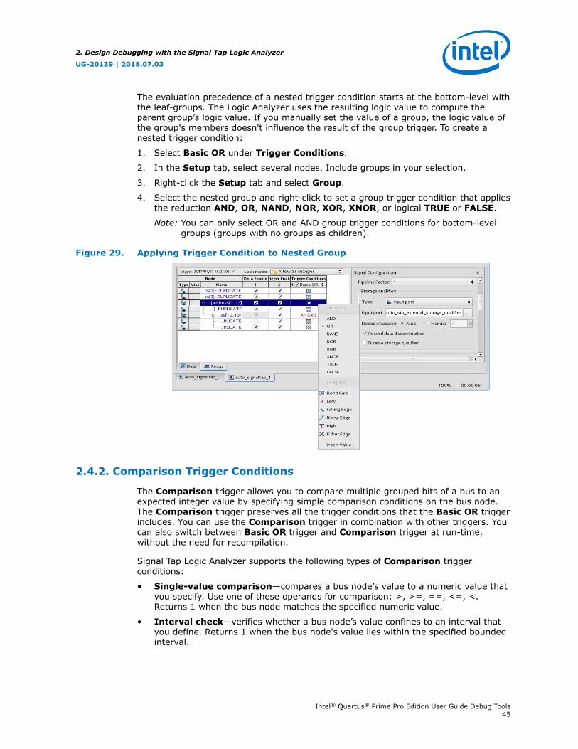
The evaluation precedence of a nested trigger condition starts at the bottom-level withthe leaf-groups. The Logic Analyzer uses the resulting logic value to compute theparent group’s logic value. If you manually set the value of a group, the logic value ofthe group's members doesn't influence the result of the group trigger. To create anested trigger condition:
1. Select Basic OR under Trigger Conditions.
2. In the Setup tab, select several nodes. Include groups in your selection.
3. Right-click the Setup tab and select Group.
4. Select the nested group and right-click to set a group trigger condition that appliesthe reduction AND, OR, NAND, NOR, XOR, XNOR, or logical TRUE or FALSE.
Note: You can only select OR and AND group trigger conditions for bottom-levelgroups (groups with no groups as children).
Figure 29. Applying Trigger Condition to Nested Group
2.4.2. Comparison Trigger Conditions
The Comparison trigger allows you to compare multiple grouped bits of a bus to anexpected integer value by specifying simple comparison conditions on the bus node.The Comparison trigger preserves all the trigger conditions that the Basic OR triggerincludes. You can use the Comparison trigger in combination with other triggers. Youcan also switch between Basic OR trigger and Comparison trigger at run-time,without the need for recompilation.
Signal Tap Logic Analyzer supports the following types of Comparison triggerconditions:
• Single-value comparison—compares a bus node’s value to a numeric value thatyou specify. Use one of these operands for comparison: >, >=, ==, <=, <.Returns 1 when the bus node matches the specified numeric value.
• Interval check—verifies whether a bus node’s value confines to an interval thatyou define. Returns 1 when the bus node's value lies within the specified boundedinterval.
2. Design Debugging with the Signal Tap Logic Analyzer
UG-20139 | 2018.07.03
Intel® Quartus® Prime Pro Edition User Guide Debug Tools45

Follow these rules when using the Comparison trigger condition:
• Apply the Comparison trigger only to bus nodes consisting of leaf nodes.
• Do not form sub-groups within a bus node.
• Do not enable or disable individual trigger nodes within a bus node.
• Do not specify comparison values (in case of single-value comparison) orboundary values (in case of interval check) exceeding the selected node’s bus-width.
2.4.2.1. Specifying the Comparison Trigger Conditions
Follow these steps to specify the Comparison trigger conditions:
1. From the Setup tab, select Comparison under Trigger Conditions.
2. Right-click the node in the trigger editor, and select Compare.
Figure 30. Selecting the Comparison Trigger Condition
Select Comparison from the Trigger Conditions list
Right-click your node and select Compare to set trigger condition values
3. Select the Comparison type from the Compare window.
— If you choose Single-value comparison as your comparison type, specifythe operand and value.
— If you choose Interval check as your comparison type, provide the lower andupper bound values for the interval.
You can also specify if you want to include or exclude the boundary values.
2. Design Debugging with the Signal Tap Logic Analyzer
UG-20139 | 2018.07.03
Intel® Quartus® Prime Pro Edition User Guide Debug Tools46

Figure 31. Specifying the Comparison ValuesCompares the bus node’s value to a specified numeric value
Verifies whether the bus node’s value confines to a specified bounded interval
Specify inclusion or exclusion of boundary values
4. Click OK. The trigger editor displays the resulting comparison expression in thegroup node condition text box.
Note: You can modify the comparison condition in the text box with a validexpression.
Figure 32. Resulting Comparison Condition in Text Box
Group node condition text box displayingthe resulting comparison expression
Modify the comparison condition in the text box with a valid expression
2.4.3. Advanced Trigger Conditions
To capture data for a given combination of conditions, build an advanced trigger. TheSignal Tap Logic Analyzer provides the Advanced Trigger tab, which helps you builda complex trigger expression using a GUI.
Open the Advanced Trigger tab by selecting Advanced in the Trigger Conditionsdrop-down menu.
2. Design Debugging with the Signal Tap Logic Analyzer
UG-20139 | 2018.07.03
Intel® Quartus® Prime Pro Edition User Guide Debug Tools47
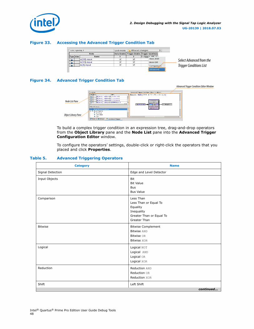
Figure 33. Accessing the Advanced Trigger Condition Tab
Select Advanced from theTrigger Conditions List
Figure 34. Advanced Trigger Condition Tab
Node List Pane
Object Library Pane
Advanced Trigger Condition Editor Window
To build a complex trigger condition in an expression tree, drag-and-drop operatorsfrom the Object Library pane and the Node List pane into the Advanced TriggerConfiguration Editor window.
To configure the operators’ settings, double-click or right-click the operators that youplaced and click Properties.
Table 5. Advanced Triggering Operators
Category Name
Signal Detection Edge and Level Detector
Input Objects BitBit ValueBusBus Value
Comparison Less ThanLess Than or Equal ToEqualityInequalityGreater Than or Equal ToGreater Than
Bitwise Bitwise ComplementBitwise ANDBitwise ORBitwise XOR
Logical Logical NOTLogical ANDLogical ORLogical XOR
Reduction Reduction ANDReduction ORReduction XOR
Shift Left Shift
continued...
2. Design Debugging with the Signal Tap Logic Analyzer
UG-20139 | 2018.07.03
Intel® Quartus® Prime Pro Edition User Guide Debug Tools48
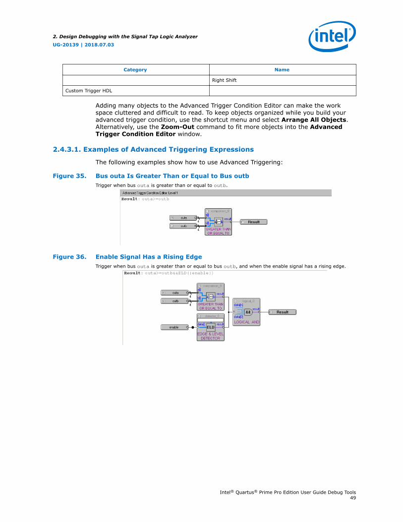
Category Name
Right Shift
Custom Trigger HDL
Adding many objects to the Advanced Trigger Condition Editor can make the workspace cluttered and difficult to read. To keep objects organized while you build youradvanced trigger condition, use the shortcut menu and select Arrange All Objects.Alternatively, use the Zoom-Out command to fit more objects into the AdvancedTrigger Condition Editor window.
2.4.3.1. Examples of Advanced Triggering Expressions
The following examples show how to use Advanced Triggering:
Figure 35. Bus outa Is Greater Than or Equal to Bus outbTrigger when bus outa is greater than or equal to outb.
Figure 36. Enable Signal Has a Rising EdgeTrigger when bus outa is greater than or equal to bus outb, and when the enable signal has a rising edge.
2. Design Debugging with the Signal Tap Logic Analyzer
UG-20139 | 2018.07.03
Intel® Quartus® Prime Pro Edition User Guide Debug Tools49

Figure 37. Bitwise AND OperationTrigger when bus outa is greater than or equal to bus outb, or when the enable signal has a rising edge. Or,when a bitwise AND operation has been performed between bus outc and bus outd, and all bits of the resultof that operation are equal to 1.
2.4.4. Custom Trigger HDL Object
Signal Tap Logic Analyzer allows you to use your own HDL module to create a customtrigger condition. You can use the Custom Trigger HDL object to simulate yourtriggering logic and ensure that the logic itself is not faulty. Additionally, you can tapinstances of modules anywhere in the hierarchy of your design, without having tomanually route all the necessary connections.
The Custom Trigger HDL object appears in the Object Library pane of the AdvancedTrigger editor.
Figure 38. Object Library
2.4.4.1. Using the Custom Trigger HDL Object
To define a custom trigger flow:
1. Select the trigger you want to edit.
2. Open the Advanced Trigger tab by selecting Advanced in the TriggerConditions drop-down menu.
3. Add to your project the HDL source file that contains the trigger module using theProject Navigator.
— Alternatively, append the HDL for your trigger module to a source file alreadyincluded in the project.
2. Design Debugging with the Signal Tap Logic Analyzer
UG-20139 | 2018.07.03
Intel® Quartus® Prime Pro Edition User Guide Debug Tools50
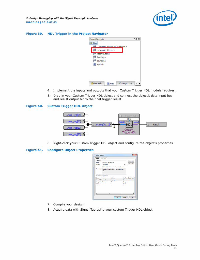
Figure 39. HDL Trigger in the Project Navigator
4. Implement the inputs and outputs that your Custom Trigger HDL module requires.
5. Drag in your Custom Trigger HDL object and connect the object’s data input busand result output bit to the final trigger result.
Figure 40. Custom Trigger HDL Object
6. Right-click your Custom Trigger HDL object and configure the object’s properties.
Figure 41. Configure Object Properties
7. Compile your design.
8. Acquire data with Signal Tap using your custom Trigger HDL object.
2. Design Debugging with the Signal Tap Logic Analyzer
UG-20139 | 2018.07.03
Intel® Quartus® Prime Pro Edition User Guide Debug Tools51

Example 2. Verilog HDL Triggers
The following trigger uses configuration bitstream:
module test_trigger ( input acq_clk, reset, input[3:0] data_in, input[1:0] pattern_in, output reg trigger_out ); always @(pattern_in) begin case (pattern_in) 2'b00: trigger_out = &data_in; 2'b01: trigger_out = |data_in; 2'b10: trigger_out = 1'b0; 2'b11: trigger_out = 1'b1; endcase endendmodule
This trigger does not have configuration bitstream:
module test_trigger_no_bs ( input acq_clk, reset, input[3:0] data_in, output reg trigger_out ); assign trigger_out = &data_in;endmodule
2.4.4.2. Required Inputs and Outputs of Custom Trigger HDL Module
Table 6. Custom Trigger HDL Module Required Inputs and Outputs
Name Description Input/Output Required/ Optional
acq_clk Acquisition clock that Signal Tap uses Input Required
reset Reset that Signal Tap uses when restarting acapture.
Input Required
data_in • Data input you connect in the AdvancedTrigger editor.
• Data your module uses to trigger.
Input Required
pattern_in • Module’s input for the configuration bitstreamproperty.
• Runtime configurable property that you canset from Signal Tap GUI to change thebehavior of your trigger logic.
Input Optional
trigger_out Output signal of your module that asserts whentrigger conditions met.
Output Required
2. Design Debugging with the Signal Tap Logic Analyzer
UG-20139 | 2018.07.03
Intel® Quartus® Prime Pro Edition User Guide Debug Tools52
2.4.4.3. Properties of Custom Trigger HDL Module
Table 7. Custom Trigger HDL Module Properties
Property Description
Custom HDL Module Name Module name of the triggering logic.
Configuration Bitstream • Allows to create trigger logic that you can configure at runtime, based uponthe value of the configuration bitstream.
• The Signal Tap logic analyzer reads the configuration bitstream property asbinary, therefore it must contain only the characters 1 and 0.
• The bit-width (number of 1s and 0s) must match the pattern_in bit width.• A blank configuration bitstream implies that the module does not have a
pattern_in input.
Pipeline Specifies the number of pipeline stages in the triggering logic.For example, if after receiving a triggering input the LA needs three clock cyclesto assert the trigger output, you can denote a pipeline value of three.
2.4.5. Trigger Condition Flow Control
The Trigger Condition Flow allows you to define the relationship between a set oftriggering conditions. Signal Tap Logic Analyzer Signal Configuration pane offers twoflow control mechanisms for organizing trigger conditions:
• Sequential Triggering—default triggering flow. Sequential triggering allows youto define up to 10 triggering levels that must be satisfied before the acquisitionbuffer finishes capturing.
• State-Based Triggering—gives the greatest control over your acquisition buffer.Custom-based triggering allows you to organize trigger conditions into statesbased on a conditional flow that you define.
You can use sequential or state based triggering with either a segmented or a non-segmented buffer.
2.4.5.1. Sequential Triggering
Sequential triggering flow allows you to cascade up to 10 levels of triggeringconditions. Signal Tap Logic Analyzer sequentially evaluates each of the conditions.
When the last triggering condition evaluates to TRUE, the Signal Tap Logic Analyzertriggers the acquisition buffer. For segmented buffers, every acquisition segment afterthe first triggers on the last condition that you specified. Use the Simple SequentialTriggering feature with basic triggers, comparison triggers, advanced triggers, or amix of all three. The figure illustrates the simple sequential triggering flow for non-segmented and segmented buffers.
The external trigger is considered as trigger level 0. The external trigger must beevaluated before the main trigger levels are evaluated.
2. Design Debugging with the Signal Tap Logic Analyzer
UG-20139 | 2018.07.03
Intel® Quartus® Prime Pro Edition User Guide Debug Tools53
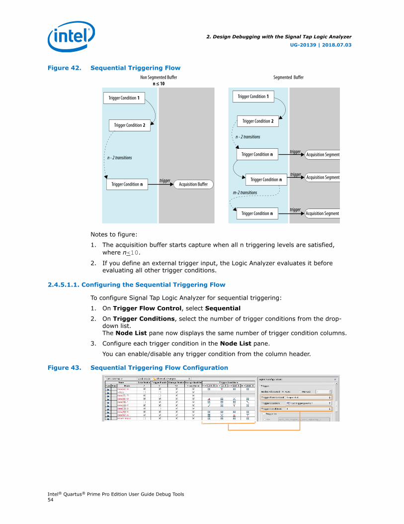
Figure 42. Sequential Triggering FlowSegmented BufferNon Segmented Buffer
n ≤ 10
Trigger Condition n
Trigger Condition 1
Trigger Condition 2
Trigger Condition 1
Trigger Condition 2
Trigger Condition n
Trigger Condition n
Trigger Condition n
n - 2 transitions
Acquisition Segment mtrigger
trigger
trigger
Acquisition Buffertrigger
n - 2 transitions
m-2 transitions
Acquisition Segment 2
Acquisition Segment 1
Notes to figure:
1. The acquisition buffer starts capture when all n triggering levels are satisfied,where n<10.
2. If you define an external trigger input, the Logic Analyzer evaluates it beforeevaluating all other trigger conditions.
2.4.5.1.1. Configuring the Sequential Triggering Flow
To configure Signal Tap Logic Analyzer for sequential triggering:
1. On Trigger Flow Control, select Sequential
2. On Trigger Conditions, select the number of trigger conditions from the drop-down list.The Node List pane now displays the same number of trigger condition columns.
3. Configure each trigger condition in the Node List pane.
You can enable/disable any trigger condition from the column header.
Figure 43. Sequential Triggering Flow Configuration
2. Design Debugging with the Signal Tap Logic Analyzer
UG-20139 | 2018.07.03
Intel® Quartus® Prime Pro Edition User Guide Debug Tools54
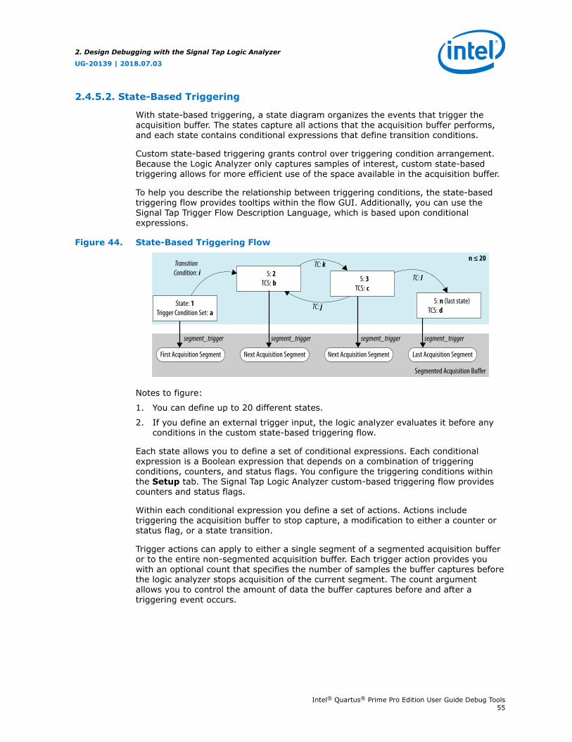
2.4.5.2. State-Based Triggering
With state-based triggering, a state diagram organizes the events that trigger theacquisition buffer. The states capture all actions that the acquisition buffer performs,and each state contains conditional expressions that define transition conditions.
Custom state-based triggering grants control over triggering condition arrangement.Because the Logic Analyzer only captures samples of interest, custom state-basedtriggering allows for more efficient use of the space available in the acquisition buffer.
To help you describe the relationship between triggering conditions, the state-basedtriggering flow provides tooltips within the flow GUI. Additionally, you can use theSignal Tap Trigger Flow Description Language, which is based upon conditionalexpressions.
Figure 44. State-Based Triggering Flow
n ≤ 20
Segmented Acquisition Buffer
First Acquisition Segment Next Acquisition Segment Next Acquisition Segment Last Acquisition Segment
Transition Condition: i
TC: j
TC: k
TC: l S: 2TCS: b S: 3
TCS: c
State: 1Trigger Condition Set: a
S: n (last state)TCS: d
segment_trigger segment_trigger segment_trigger segment_trigger
Notes to figure:
1. You can define up to 20 different states.
2. If you define an external trigger input, the logic analyzer evaluates it before anyconditions in the custom state-based triggering flow.
Each state allows you to define a set of conditional expressions. Each conditionalexpression is a Boolean expression that depends on a combination of triggeringconditions, counters, and status flags. You configure the triggering conditions withinthe Setup tab. The Signal Tap Logic Analyzer custom-based triggering flow providescounters and status flags.
Within each conditional expression you define a set of actions. Actions includetriggering the acquisition buffer to stop capture, a modification to either a counter orstatus flag, or a state transition.
Trigger actions can apply to either a single segment of a segmented acquisition bufferor to the entire non-segmented acquisition buffer. Each trigger action provides youwith an optional count that specifies the number of samples the buffer captures beforethe logic analyzer stops acquisition of the current segment. The count argumentallows you to control the amount of data the buffer captures before and after atriggering event occurs.
2. Design Debugging with the Signal Tap Logic Analyzer
UG-20139 | 2018.07.03
Intel® Quartus® Prime Pro Edition User Guide Debug Tools55
Resource manipulation actions allow you to increment and decrement counters or setand clear status flags. The logic analyzer uses counter and status flag resources asoptional inputs in conditional expressions. Counters and status flags are useful forcounting the number of occurrences of certain events and for aiding in triggering flowcontrol.
The state-based triggering flow allows you to capture a sequence of events that maynot necessarily be contiguous in time. For example, a communication transactionbetween two devices that includes a hand shaking protocol containing a sequence ofacknowledgements.
2.4.5.2.1. State-Based Triggering Flow Tab
The State-Based Trigger Flow tab is the control interface for the custom state-based triggering flow.
This tab is only available when you select State-Based on the Trigger Flow Controllist. If you specify Trigger Flow Control as Sequential, the State-Based TriggerFlow tab is not visible.
Figure 45. State-Based Triggering Flow Tab
The State-Based Trigger Flow tab contains three panes:
State Diagram Pane
The State Diagram pane provides a graphical overview of your triggering flow. thispane displays the number of available states and the state transitions. To adjust thenumber of available states, use the menu above the graphical overview.
2. Design Debugging with the Signal Tap Logic Analyzer
UG-20139 | 2018.07.03
Intel® Quartus® Prime Pro Edition User Guide Debug Tools56
State Machine Pane
The State Machine pane contains the text entry boxes where you define thetriggering flow and actions associated with each state.
• You can define the triggering flow using the Signal Tap Trigger Flow DescriptionLanguage, a simple language based on “if-else” conditional statements.
• Tooltips appear when you move the mouse over the cursor, to guide commandentry into the state boxes.
• The GUI provides a syntax check on your flow description in real-time andhighlights any errors in the text flow.
The State Machine description text boxes default to show one text box per state. Youcan also have the entire flow description shown in a single text field. This option canbe useful when copying and pasting a flow description from a template or an externaltext editor. To toggle between one window per state, or all states in one window,select the appropriate option under State Display mode.
Related Information
Signal Tap Trigger Flow Description Language on page 58
Resources Pane
The Resources pane allows you to declare status flags and counters for your CustomTriggering Flow's conditional expressions.
• You can increment/decrement counters or set/clear status flags within yourtriggering flow.
• You can specify up to 20 counters and 20 status flags.
• To initialize counter and status flags, right-click the row in the table and select SetInitial Value.
• To specify a counter width, right-click the counter in the table and select SetWidth.
• To assist in debugging your trigger flow specification, the logic analyzerdynamically updates counters and flag values after acquisition starts.
The Configurable at runtime settings allow you to control which options can changeat runtime without requiring a recompilation.
Table 8. Runtime Reconfigurable Settings, State-Based Triggering Flow
Setting Description
Destination of goto action Allows you to modify the destination of the state transition at runtime.
Comparison values Allows you to modify comparison values in Boolean expressions at runtime. Inaddition, you can modify the segment_trigger and trigger action post-fillcount argument at runtime.
Comparison operators Allows you to modify the operators in Boolean expressions at runtime.
Logical operators Allows you to modify the logical operators in Boolean expressions at runtime.
Related Information
• Performance and Resource Considerations on page 70
• Runtime Reconfigurable Options on page 73
2. Design Debugging with the Signal Tap Logic Analyzer
UG-20139 | 2018.07.03
Intel® Quartus® Prime Pro Edition User Guide Debug Tools57

2.4.5.2.2. Trigger Lock Mode
Trigger lock mode restricts changes to only the configuration settings that you specifyas Configurable at runtime. The runtime configurable settings for the CustomTrigger Flow tab are on by default.
Note: You may get some performance advantages by disabling some of the runtimeconfigurable options.
You can restrict changes to your Signal Tap configuration to include only the optionsthat do not require a recompilation. Trigger lock-mode allows you to make changesthat reflect immediately in the device.
1. On the Setup tab, point to Lock Mode and select Allow trigger conditionchanges only.
Figure 46. Allow Trigger Conditions Change Only
2. Modify the Trigger Flow conditions.
2.4.5.3. Signal Tap Trigger Flow Description Language
The Trigger Flow Description Language is based on a list of conditional expressions perstate to define a set of actions.
To describe the actions the Logic Analyzer evaluates when a state is reached, youfollow this syntax:
Syntax of Trigger Flow Description Language
state <state_label>: <action_list> if (<boolean_expression>) <action_list> [else if (<boolean_expression>) <action_list>] [else <action_list>]
• Non-terminals are delimited by "<>".
• Optional arguments are delimited by "[]"
• The priority for evaluation of conditional statements is from top to bottom.
• The Trigger Flow Description Language allows multiple else if conditions.
<state_label> on page 59
<boolean_expression> on page 59
<action_list> on page 60
Related Information
Custom Triggering Flow Application Examples on page 90
2. Design Debugging with the Signal Tap Logic Analyzer
UG-20139 | 2018.07.03
Intel® Quartus® Prime Pro Edition User Guide Debug Tools58

2.4.5.3.1. <state_label>
Identifies a given state. You use the state label to start describing the actions theLogic Analyzer evaluates once said state is reached. You can also use the state labelwith the goto command.
The state description header syntax is:state <state_label>
The description of a state ends with the beginning of another state or the end of thewhole trigger flow description.
2.4.5.3.2. <boolean_expression>
Collection of operators and operands that evaluate into a Boolean result. Theoperators can be logical or relational. Depending on the operator, the operand canreference a trigger condition, a counter and a register, or a numeric value. To group aset of operands within an expression, you use parentheses.
Table 9. Logical OperatorsLogical operators accept any boolean expression as an operand.
Operator Description Syntax
! NOT operator ! expr1
&& AND operator expr1 && expr2
|| OR operator expr1 || expr2
Table 10. Relational OperatorsYou use relational operators on counters or status flags.
Operator Description Syntax
> Greater than <identifier> > <numerical_value>
>= Greater than or Equalto
<identifier> >= <numerical_value>
== Equals <identifier> == <numerical_value>
!= Does not equal <identifier> != <numerical_value>
<= Less than or equal to <identifier> <= <numerical_value>
< Less than <identifier> < <numerical_value>
Notes to table:1. <identifier> indicates a counter or status flag.2. <numerical_value> indicates an integer.
Note: • The <boolean_expression> in an if statement can contain a single event ormultiple event conditions.
• When the boolean expression evaluates TRUE, the logic analyzer evaluates all thecommands in the <action_list> concurrently.
2. Design Debugging with the Signal Tap Logic Analyzer
UG-20139 | 2018.07.03
Intel® Quartus® Prime Pro Edition User Guide Debug Tools59
2.4.5.3.3. <action_list>
List of actions that the Logic Analyzer performs within a state once a condition issatisfied.
• Each action must end with a semicolon (;).
• If you specify more than one action within an if or an else if clause, you mustdelimit the action_list with begin and end tokens.
Possible actions include:
Resource Manipulation Action
The resources the trigger flow description uses can be either counters or status flags.
Table 11. Resource Manipulation Actions
Action Description Syntax
increment Increments a counter resource by 1 increment <counter_identifier>;
decrement Decrements a counter resource by 1 decrement <counter_identifier>;
reset Resets counter resource to initial value reset <counter_identifier>;
set Sets a status flag to 1 set <register_flag_identifier>;
clear Sets a status flag to 0 clear <register_flag_identifier>;
Buffer Control Actions
Actions that control the acquisition buffer.
Table 12. Buffer Control Actions
Action Description Syntax
trigger Stops the acquisition for the current buffer andends analysis. This command is required in everyflow definition.
trigger <post-fill_count>;
segment_trigger Available only in segmented acquisition mode.Ends acquisition of the current segment. Afterevaluating this command, the Signal Tap LogicAnalyzer starts acquiring from the next segment. Ifall segments are written, the Logic Analyzeroverwrites the oldest segment with the latestsample. When a trigger action is evaluated theacquisition stops.
segment_trigger <post-fill_count>;
start_store Active only in state-based storage qualifier mode.Asserts the write_enable to the Signal Tapacquisition buffer.
start_store
stop_store Active only in state-based storage qualifier mode.De-asserts the write_enable signal to the SignalTap acquisition buffer.
stop_store
Both trigger and segment_trigger actions accept an optional post-fill_countargument.
2. Design Debugging with the Signal Tap Logic Analyzer
UG-20139 | 2018.07.03
Intel® Quartus® Prime Pro Edition User Guide Debug Tools60
Related Information
Post-fill Count on page 65
State Transition Action
Specifies the next state in the custom state control flow. The syntax is:goto <state_label>;
2.4.5.4. Using the State-Based Storage Qualifier Feature
Selecting a state-based storage qualifier type enables the start_store andstop_store actions. When you use these actions in conjunction with the expressionsof the State-based trigger flow, you get maximum flexibility to control data writteninto the acquisition buffer.
Note: You can only apply the start_store and stop_store commands to a non-segmented buffer.
The start_store and stop_store commands are similar to the start and stopconditions of the start/stop storage qualifier mode. If you enable storagequalification, Signal Tap Logic Analyzer doesn't write data into the acquisition bufferuntil the start_store command occurs. However, in the state-based storagequalifier type you must include a trigger command as part of the trigger flowdescription. This trigger command is necessary to complete the acquisition anddisplay the results on the waveform display.
2.4.5.4.1. Storage Qualification Feature for the State-Based Trigger Flow.
This trigger flow description contains three trigger conditions that happen at differenttimes after you click Start Analysis:
State 1: ST1: if ( condition1 ) start_store; else if ( condition2 ) trigger value; else if ( condition3 ) stop_store;
Figure 47. Capture Scenario for Storage Qualification with the State-Based Trigger Flow
When you apply the trigger flow to the scenario in the figure:
a b c Sample
n samples
m samples
Time Scale for data streamat the start of acquisition
Condition 1 occurs Condition 3 occursCondition 2 occurs
2. Design Debugging with the Signal Tap Logic Analyzer
UG-20139 | 2018.07.03
Intel® Quartus® Prime Pro Edition User Guide Debug Tools61
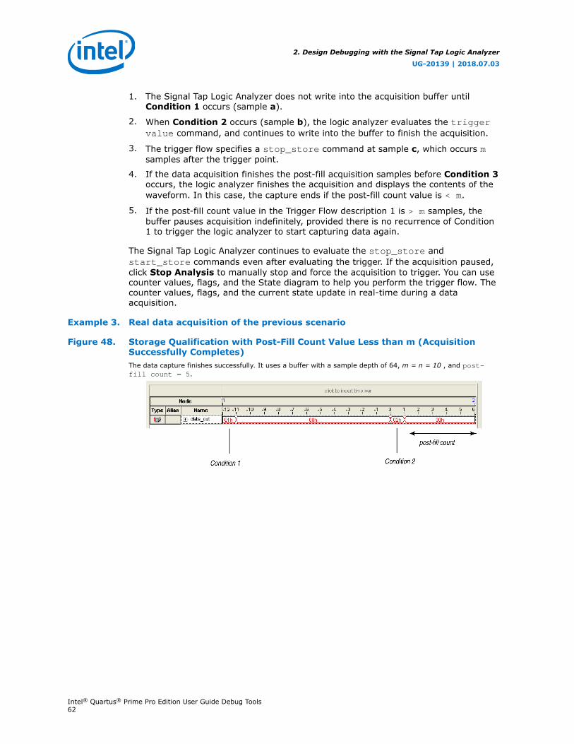
1. The Signal Tap Logic Analyzer does not write into the acquisition buffer untilCondition 1 occurs (sample a).
2. When Condition 2 occurs (sample b), the logic analyzer evaluates the triggervalue command, and continues to write into the buffer to finish the acquisition.
3. The trigger flow specifies a stop_store command at sample c, which occurs msamples after the trigger point.
4. If the data acquisition finishes the post-fill acquisition samples before Condition 3occurs, the logic analyzer finishes the acquisition and displays the contents of thewaveform. In this case, the capture ends if the post-fill count value is < m.
5. If the post-fill count value in the Trigger Flow description 1 is > m samples, thebuffer pauses acquisition indefinitely, provided there is no recurrence of Condition1 to trigger the logic analyzer to start capturing data again.
The Signal Tap Logic Analyzer continues to evaluate the stop_store andstart_store commands even after evaluating the trigger. If the acquisition paused,click Stop Analysis to manually stop and force the acquisition to trigger. You can usecounter values, flags, and the State diagram to help you perform the trigger flow. Thecounter values, flags, and the current state update in real-time during a dataacquisition.
Example 3. Real data acquisition of the previous scenario
Figure 48. Storage Qualification with Post-Fill Count Value Less than m (AcquisitionSuccessfully Completes)The data capture finishes successfully. It uses a buffer with a sample depth of 64, m = n = 10 , and post-fill count = 5.
2. Design Debugging with the Signal Tap Logic Analyzer
UG-20139 | 2018.07.03
Intel® Quartus® Prime Pro Edition User Guide Debug Tools62
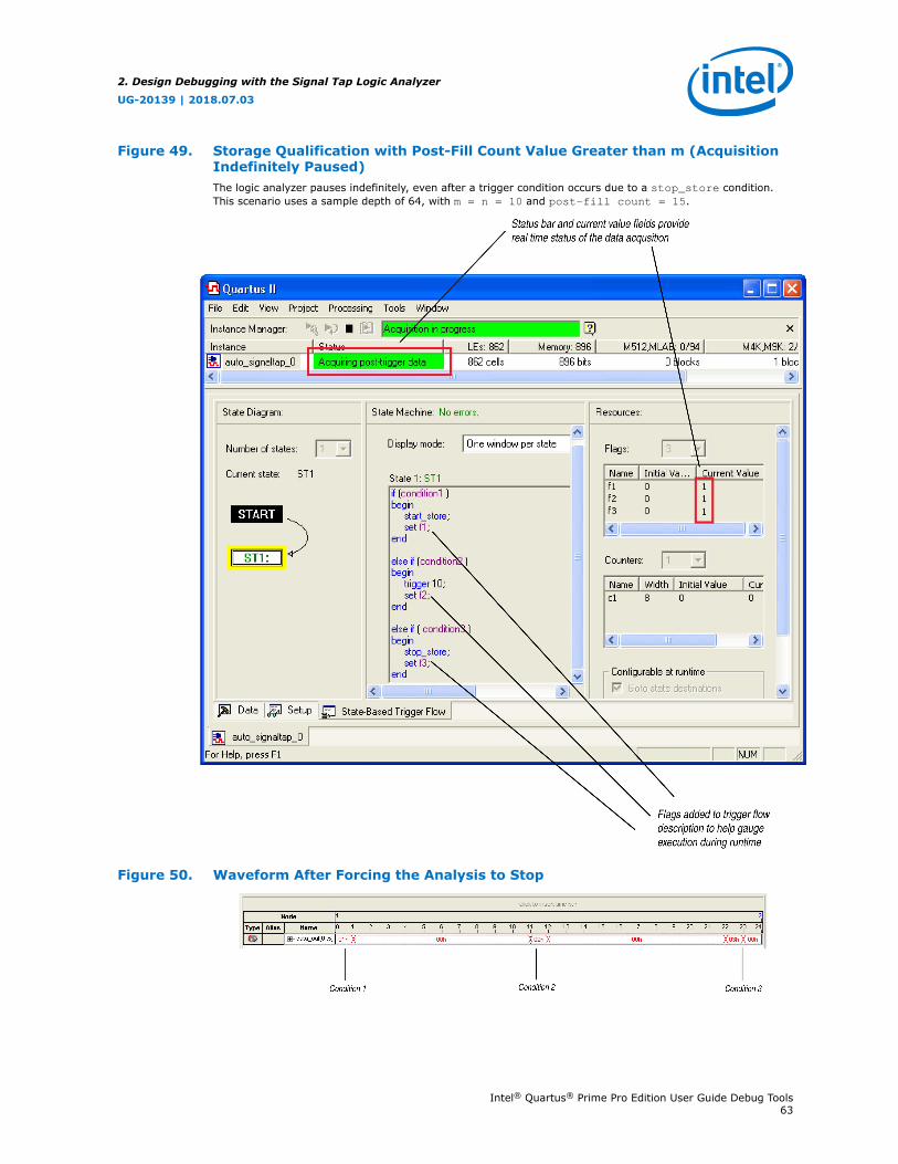
Figure 49. Storage Qualification with Post-Fill Count Value Greater than m (AcquisitionIndefinitely Paused)The logic analyzer pauses indefinitely, even after a trigger condition occurs due to a stop_store condition.This scenario uses a sample depth of 64, with m = n = 10 and post-fill count = 15.
Figure 50. Waveform After Forcing the Analysis to Stop
2. Design Debugging with the Signal Tap Logic Analyzer
UG-20139 | 2018.07.03
Intel® Quartus® Prime Pro Edition User Guide Debug Tools63
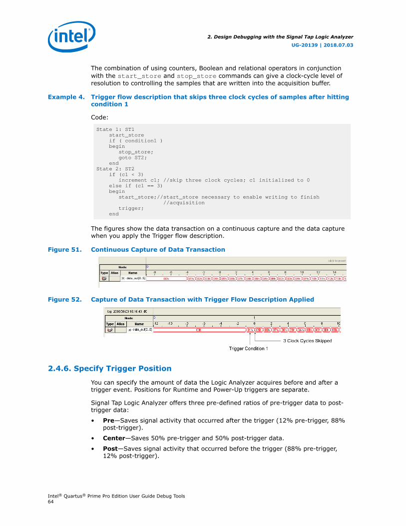
The combination of using counters, Boolean and relational operators in conjunctionwith the start_store and stop_store commands can give a clock-cycle level ofresolution to controlling the samples that are written into the acquisition buffer.
Example 4. Trigger flow description that skips three clock cycles of samples after hittingcondition 1
Code:
State 1: ST1 start_store if ( condition1 ) begin stop_store; goto ST2; endState 2: ST2 if (c1 < 3) increment c1; //skip three clock cycles; c1 initialized to 0 else if (c1 == 3) begin start_store;//start_store necessary to enable writing to finish //acquisition trigger; end
The figures show the data transaction on a continuous capture and the data capturewhen you apply the Trigger flow description.
Figure 51. Continuous Capture of Data Transaction
Figure 52. Capture of Data Transaction with Trigger Flow Description Applied
2.4.6. Specify Trigger Position
You can specify the amount of data the Logic Analyzer acquires before and after atrigger event. Positions for Runtime and Power-Up triggers are separate.
Signal Tap Logic Analyzer offers three pre-defined ratios of pre-trigger data to post-trigger data:
• Pre—Saves signal activity that occurred after the trigger (12% pre-trigger, 88%post-trigger).
• Center—Saves 50% pre-trigger and 50% post-trigger data.
• Post—Saves signal activity that occurred before the trigger (88% pre-trigger,12% post-trigger).
2. Design Debugging with the Signal Tap Logic Analyzer
UG-20139 | 2018.07.03
Intel® Quartus® Prime Pro Edition User Guide Debug Tools64

These pre-defined ratios apply to both non-segmented buffers and segmented buffers.
Related Information
State-Based Triggering on page 55
2.4.6.1. Post-fill Count
In a custom state-based triggering flow with the segment_trigger and triggerbuffer control actions, you can use the post-fill_count argument to specify acustom trigger position.
• If you do not use the post-fill_count argument, the trigger position for theaffected buffer defaults to the trigger position you specified in the Setup tab.
• In the trigger buffer control action (for non-segmented buffers), post-fill_count specifies the number of samples to capture before stopping dataacquisition.
• In the segment_trigger buffer control action (for segmented buffer), post-fill_count specifies a data segment.
Note: In the case of segment_trigger, acquisition of the current buffer stopsimmediately if a subsequent triggering action is issued in the next state,regardless of the current buffer's post-fill count. The Logic Analyzer discardsthe remaining unfilled post-count acquisitions in the current buffer, anddisplays them as grayed-out samples in the data window.
When the Signal Tap data window displays the captured data, the trigger positionappears as the number of post-count samples from the end of the acquisition segmentor buffer.
Sample Number of Trigger Position = (N – Post-Fill Count)
In this case, N is the sample depth of either the acquisition segment or non-segmented buffer.
Related Information
Buffer Control Actions on page 60
2.4.7. Power-Up Triggers
Power-up triggers capture events that occur during device initialization, immediatelyafter you power or reset the FPGA.
The typical use of Signal Tap Logic Analyzer is triggering events that occur duringnormal device operation. You start an analysis manually once the target device is fullypowered on and the JTAG connection for the device is available. With Signal TapPower-Up Trigger feature, the Signal Tap Logic Analyzer captures data immediatelyafter device initialization.
You can add a different Power-Up Trigger to each logic analyzer instance in the SignalTap Instance Manager pane.
2. Design Debugging with the Signal Tap Logic Analyzer
UG-20139 | 2018.07.03
Intel® Quartus® Prime Pro Edition User Guide Debug Tools65
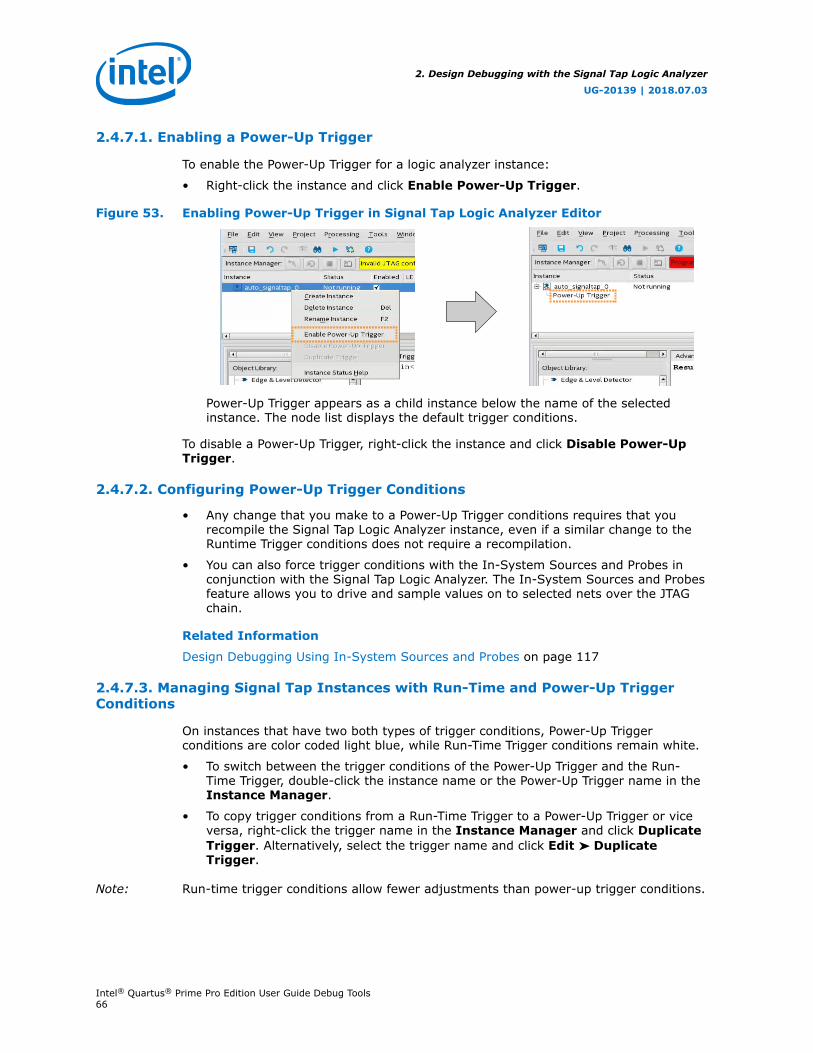
2.4.7.1. Enabling a Power-Up Trigger
To enable the Power-Up Trigger for a logic analyzer instance:
• Right-click the instance and click Enable Power-Up Trigger.
Figure 53. Enabling Power-Up Trigger in Signal Tap Logic Analyzer Editor
Power-Up Trigger appears as a child instance below the name of the selectedinstance. The node list displays the default trigger conditions.
To disable a Power-Up Trigger, right-click the instance and click Disable Power-UpTrigger.
2.4.7.2. Configuring Power-Up Trigger Conditions
• Any change that you make to a Power-Up Trigger conditions requires that yourecompile the Signal Tap Logic Analyzer instance, even if a similar change to theRuntime Trigger conditions does not require a recompilation.
• You can also force trigger conditions with the In-System Sources and Probes inconjunction with the Signal Tap Logic Analyzer. The In-System Sources and Probesfeature allows you to drive and sample values on to selected nets over the JTAGchain.
Related Information
Design Debugging Using In-System Sources and Probes on page 117
2.4.7.3. Managing Signal Tap Instances with Run-Time and Power-Up TriggerConditions
On instances that have two both types of trigger conditions, Power-Up Triggerconditions are color coded light blue, while Run-Time Trigger conditions remain white.
• To switch between the trigger conditions of the Power-Up Trigger and the Run-Time Trigger, double-click the instance name or the Power-Up Trigger name in theInstance Manager.
• To copy trigger conditions from a Run-Time Trigger to a Power-Up Trigger or viceversa, right-click the trigger name in the Instance Manager and click DuplicateTrigger. Alternatively, select the trigger name and click Edit ➤ DuplicateTrigger.
Note: Run-time trigger conditions allow fewer adjustments than power-up trigger conditions.
2. Design Debugging with the Signal Tap Logic Analyzer
UG-20139 | 2018.07.03
Intel® Quartus® Prime Pro Edition User Guide Debug Tools66
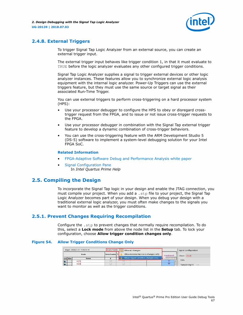
2.4.8. External Triggers
To trigger Signal Tap Logic Analyzer from an external source, you can create anexternal trigger input.
The external trigger input behaves like trigger condition 1, in that it must evaluate toTRUE before the logic analyzer evaluates any other configured trigger conditions.
Signal Tap Logic Analyzer supplies a signal to trigger external devices or other logicanalyzer instances. These features allow you to synchronize external logic analysisequipment with the internal logic analyzer. Power-Up Triggers can use the externaltriggers feature, but they must use the same source or target signal as theirassociated Run-Time Trigger.
You can use external triggers to perform cross-triggering on a hard processor system(HPS):
• Use your processor debugger to configure the HPS to obey or disregard cross-trigger request from the FPGA, and to issue or not issue cross-trigger requests tothe FPGA.
• Use your processor debugger in combination with the Signal Tap external triggerfeature to develop a dynamic combination of cross-trigger behaviors.
• You can use the cross-triggering feature with the ARM Development Studio 5(DS-5) software to implement a system-level debugging solution for your IntelFPGA SoC.
Related Information
• FPGA-Adaptive Software Debug and Performance Analysis white paper
• Signal Configuration PaneIn Intel Quartus Prime Help
2.5. Compiling the Design
To incorporate the Signal Tap logic in your design and enable the JTAG connection, youmust compile your project. When you add a .stp file to your project, the Signal TapLogic Analyzer becomes part of your design. When you debug your design with atraditional external logic analyzer, you must often make changes to the signals youwant to monitor as well as the trigger conditions.
2.5.1. Prevent Changes Requiring Recompilation
Configure the .stp to prevent changes that normally require recompilation. To dothis, select a Lock mode from above the node list in the Setup tab. To lock yourconfiguration, choose Allow trigger condition changes only.
Figure 54. Allow Trigger Conditions Change Only
2. Design Debugging with the Signal Tap Logic Analyzer
UG-20139 | 2018.07.03
Intel® Quartus® Prime Pro Edition User Guide Debug Tools67

Related Information
Verify Whether You Need to Recompile Your Project on page 68
2.5.2. Verify Whether You Need to Recompile Your Project
Before starting a debugging session, do not make any changes to the .stp settingsthat require recompiling the project.
To verify whether a change you made requires recompiling the project, check theSignal Tap status display at the top of the Instance Manager pane. This featureallows you to undo the change, so that you do not need to recompile your project.
Related Information
Prevent Changes Requiring Recompilation on page 67
2.5.3. Incremental Route with Rapid Recompile
You can use Incremental Route with Rapid Recompile to decrease compilation times.After performing a full compilation on your design, you can use the Incremental Routeflow to achieve a 2-4x speedup over a flat compile. The Incremental Route flow is notcompatible with Partial Reconfiguration.
Intel Quartus Prime Pro Edition software supports Incremental Route with RapidRecompile for Intel Arria® 10, Intel Cyclone® 10 GX, and Intel Stratix 10 devicefamilies.
Related Information
Running Rapid RecompileIn Compiler User Guide: Intel Quartus Prime Pro Edition
2.5.3.1. Using the Incremental Route Flow
To use the Incremental Route flow:
1. Open your design and run Analysis & Elaboration (or a full compilation) to givenode visibility in Signal Tap.
2. Add Signal Tap to your design.
3. In the Signal Tap Signal Configuration pane, specify Manual in the NodesAllocated field for Trigger and Data nodes (and Storage Qualifier, if used).
2. Design Debugging with the Signal Tap Logic Analyzer
UG-20139 | 2018.07.03
Intel® Quartus® Prime Pro Edition User Guide Debug Tools68
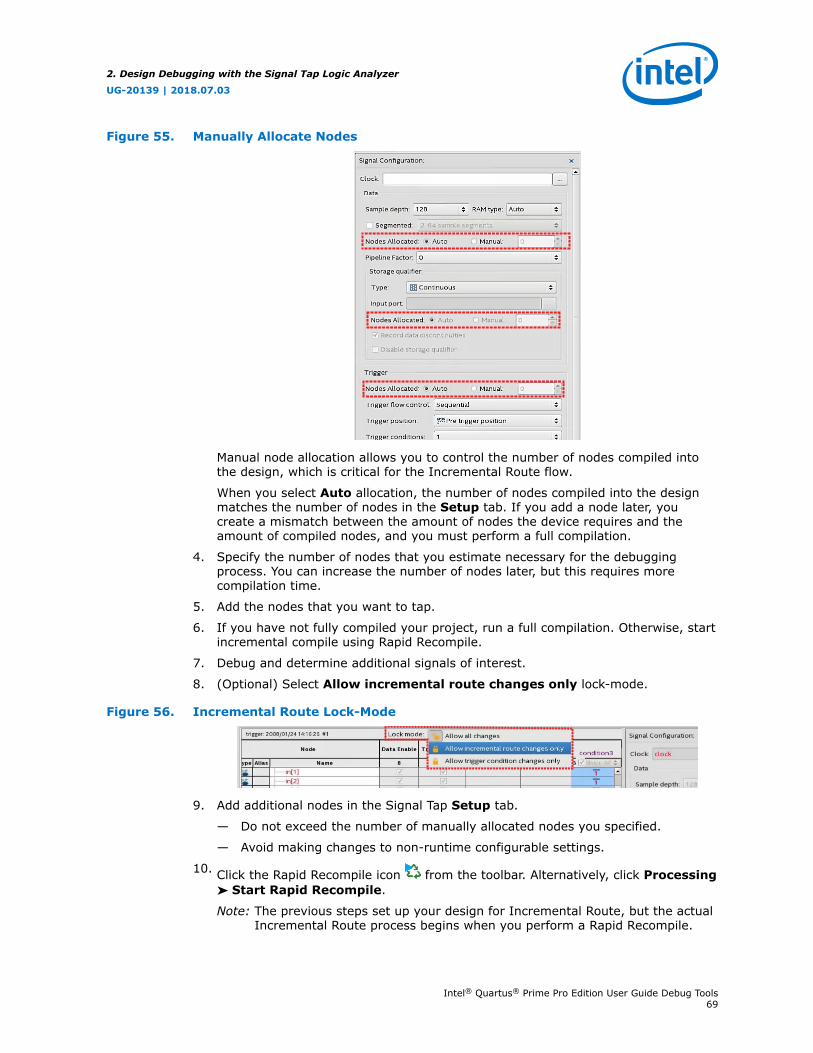
Figure 55. Manually Allocate Nodes
Manual node allocation allows you to control the number of nodes compiled intothe design, which is critical for the Incremental Route flow.
When you select Auto allocation, the number of nodes compiled into the designmatches the number of nodes in the Setup tab. If you add a node later, youcreate a mismatch between the amount of nodes the device requires and theamount of compiled nodes, and you must perform a full compilation.
4. Specify the number of nodes that you estimate necessary for the debuggingprocess. You can increase the number of nodes later, but this requires morecompilation time.
5. Add the nodes that you want to tap.
6. If you have not fully compiled your project, run a full compilation. Otherwise, startincremental compile using Rapid Recompile.
7. Debug and determine additional signals of interest.
8. (Optional) Select Allow incremental route changes only lock-mode.
Figure 56. Incremental Route Lock-Mode
9. Add additional nodes in the Signal Tap Setup tab.
— Do not exceed the number of manually allocated nodes you specified.
— Avoid making changes to non-runtime configurable settings.
10. Click the Rapid Recompile icon from the toolbar. Alternatively, click Processing➤ Start Rapid Recompile.
Note: The previous steps set up your design for Incremental Route, but the actualIncremental Route process begins when you perform a Rapid Recompile.
2. Design Debugging with the Signal Tap Logic Analyzer
UG-20139 | 2018.07.03
Intel® Quartus® Prime Pro Edition User Guide Debug Tools69
2.5.3.2. Tips to Achieve Maximum Speedup
• Basic AND (which applies to Storage Qualifier as well as trigger input) is thefastest for the Incremental Route flow.
• Basic OR is slower for the Incremental Route flow, but if you avoid changing theparent-child relationship of nodes within groups, you can minimize the impact oncompile time. You can change the sibling relationships of nodes.
— Basic OR and advanced triggers require re-synthesis when you change thenumber/names of tapped nodes.
• Use the Incremental Route lock-mode to avoid inadvertent changes requiring a fullcompilation.
2.5.4. Timing Preservation with the Signal Tap Logic Analyzer
In addition to verifying functionality, timing closure is one of the most crucialprocesses in successful operation of your design.
The Intel Quartus Prime Pro Edition software supports timing preservation for post-fittaps in Intel Arria 10 designs with the Rapid Recompile feature. Rapid Recompileautomatically reuses verified portions of your design during recompilations, ratherthan reprocessing those portions.
Note: The Signal Tap Intel FPGA IP is not optimized for the Intel Stratix 10 architecture.
Use the following techniques to help maintain timing:
• Avoid adding critical path signals to your .stp.
• Minimize the number of combinational signals you add to your .stp, and addregisters whenever possible.
• Specify an fMAX constraint for each clock in your design.
Related Information
Timing Closure and OptimizationIn Design Optimization User Guide: Intel Quartus Prime Pro Edition
2.5.5. Performance and Resource Considerations
When you perform logic analysis of your design, you can see the necessary trade-offbetween runtime flexibility, timing performance, and resource usage.
The Signal Tap Logic Analyzer allows you to select runtime configurable parameters tobalance the need for runtime flexibility, speed, and area.
The default values of the runtime configurable parameters provide maximumflexibility, so you can complete debugging as quickly as possible; however, you canadjust these settings to determine whether there is a more appropriate configurationfor your design. Because performance results are design-dependent, try these optionsin different combinations until you achieve the desired balance between functionality,performance, and utilization.
2. Design Debugging with the Signal Tap Logic Analyzer
UG-20139 | 2018.07.03
Intel® Quartus® Prime Pro Edition User Guide Debug Tools70

2.5.5.1. Signal Tap Logic in Critical Path
If Signal Tap logic is part of your critical path, follow these tips to speed up theperformance of the Signal Tap Logic Analyzer:
• Disable runtime configurable options—Certain resources are allocated toaccommodate for runtime flexibility. If you use either advanced triggers or State-based triggering flow, disable runtime configurable parameters for a boost in fMAXof the Signal Tap logic.
— If you are using State-based triggering flow, try disabling the Goto statedestination option and performing a recompilation before disabling the otherruntime configurable options. The Goto state destination option has thegreatest impact on fMAX, as compared to the other runtime configurableoptions.
• Minimize the number of signals that have Trigger Enable selected—Bydefault, Signal Tap Logic Analyzer enable the Trigger Enable option for all signalsthat you add to the .stp file. For signals that you do not plan to use as triggers,turn this option off.
• Turn on Physical Synthesis for register retiming—If many (more than thenumber of inputs that fit in a LAB) enabled triggering signals fan-in logic to agate-based triggering condition (basic trigger condition or a logical reductionoperator in the advanced trigger tab), turn on Perform register retiming. Thiscan help balance combinational logic across LABs.
2.5.5.2. Signal Tap Logic Using Critical Resources
If your design is resource constrained, follow these tips to reduce the logic or memorythe Signal Tap Logic Analyzer uses:
• Disable runtime configurable options—Disabling runtime configurability foradvanced trigger conditions or runtime configurable options in the State-basedtriggering flow results in fewer LEs.
• Minimize the number of segments in the acquisition buffer—You can reducethe logic resources that the Signal Tap Logic Analyzer uses if you limit thesegments in your sampling buffer
• Disable the Data Enable for signals that you use only for triggering—Bydefault, Signal Tap Logic Analyzer enables data enable options for all signals.Turning off the data enable option for signals you use only as trigger inputs saveson memory resources.
2.6. Program the Target Device or Devices
After you add the Signal Tap Logic Analyzer to your project and re-compile, you canconfigure the FPGA target device.
If you want to debug multiple designs simultaneously, configure the device fromthe .stp instead of the Intel Quartus Prime Programmer. This allows you to openmore than one .stp file and program multiple devices.
2. Design Debugging with the Signal Tap Logic Analyzer
UG-20139 | 2018.07.03
Intel® Quartus® Prime Pro Edition User Guide Debug Tools71

2.6.1. Ensure Setting Compatibility Between .stp and .sof Files
A .stp file is compatible with a .sof file when the settings for the logic analyzer,such as the size of the capture buffer and the signals you use for monitoring ortriggering, match the programming settings of the target device. If the files are notcompatible, you can still program the device, but you cannot run or control the logicanalyzer from the Signal Tap Logic Analyzer Editor.
• To ensure programming compatibility, program your device with the .sof filegenerated in the most recent compilation.
• To check whether a particular .sof is compatible with the current Signal Tapconfiguration, attach the .sof to the SOF manager.
Note: When the Signal Tap Logic Analyzer detects incompatibility after the analysis starts,the Intel Quartus Prime software generates a system error message containing twoCRC values: the expected value and the value retrieved from the .stp instance on thedevice. The CRC value comes from all Signal Tap settings that affect the compilation.
Although having a Intel Quartus Prime project is not required when using an .stp, itis recommended. The project database contains information about the integrity of thecurrent Signal Tap Logic Analyzer session. Without the project database, there is noway to verify that the current .stp file matches the .sof file in the device. If youhave an .stp file that does not match the .sof file, the Signal Tap Logic Analyzer cancapture incorrect data.
Related Information
Manage Multiple Signal Tap Files and Configurations on page 42
2.7. Running the Signal Tap Logic Analyzer
Debugging Signal Tap Logic Analyzer is similar using an external logic analyzer. Youinitialize the logic analyzer by starting an analysis. When your trigger event occurs,the logic analyzer stores the captured data in the device's memory buffer, and thentransfers this data to the .stp file with the JTAG connection.
You can also perform the equivalent of a force trigger instruction that lets you viewthe captured data currently in the buffer without a trigger event occurring.
The flowchart shows how you operate the Signal Tap Logic Analyzer. indicates wherePower-Up and Runtime Trigger events occur and when captured data from theseevents is available for analysis.
2. Design Debugging with the Signal Tap Logic Analyzer
UG-20139 | 2018.07.03
Intel® Quartus® Prime Pro Edition User Guide Debug Tools72
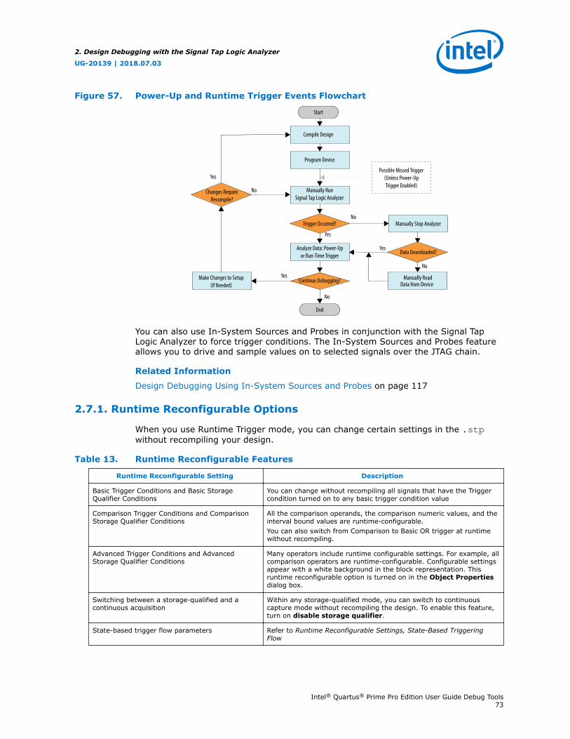
Figure 57. Power-Up and Runtime Trigger Events Flowchart
Manually RunSignal Tap Logic Analyzer
Compile Design
Start
End
Yes
No
No
Yes
Yes
No
Program Device
No
Yes
Manually Read Data from Device
Trigger Occurred?
Analyze Data: Power-Upor Run-Time Trigger
Continue Debugging?Make Changes to Setup(If Needed)
Changes RequireRecompile?
Data Downloaded?
Manually Stop Analyzer
Possible Missed Trigger(Unless Power-UpTrigger Enabled)
You can also use In-System Sources and Probes in conjunction with the Signal TapLogic Analyzer to force trigger conditions. The In-System Sources and Probes featureallows you to drive and sample values on to selected signals over the JTAG chain.
Related Information
Design Debugging Using In-System Sources and Probes on page 117
2.7.1. Runtime Reconfigurable Options
When you use Runtime Trigger mode, you can change certain settings in the .stpwithout recompiling your design.
Table 13. Runtime Reconfigurable Features
Runtime Reconfigurable Setting Description
Basic Trigger Conditions and Basic StorageQualifier Conditions
You can change without recompiling all signals that have the Triggercondition turned on to any basic trigger condition value
Comparison Trigger Conditions and ComparisonStorage Qualifier Conditions
All the comparison operands, the comparison numeric values, and theinterval bound values are runtime-configurable.You can also switch from Comparison to Basic OR trigger at runtimewithout recompiling.
Advanced Trigger Conditions and AdvancedStorage Qualifier Conditions
Many operators include runtime configurable settings. For example, allcomparison operators are runtime-configurable. Configurable settingsappear with a white background in the block representation. Thisruntime reconfigurable option is turned on in the Object Propertiesdialog box.
Switching between a storage-qualified and acontinuous acquisition
Within any storage-qualified mode, you can switch to continuouscapture mode without recompiling the design. To enable this feature,turn on disable storage qualifier.
State-based trigger flow parameters Refer to Runtime Reconfigurable Settings, State-Based TriggeringFlow
2. Design Debugging with the Signal Tap Logic Analyzer
UG-20139 | 2018.07.03
Intel® Quartus® Prime Pro Edition User Guide Debug Tools73
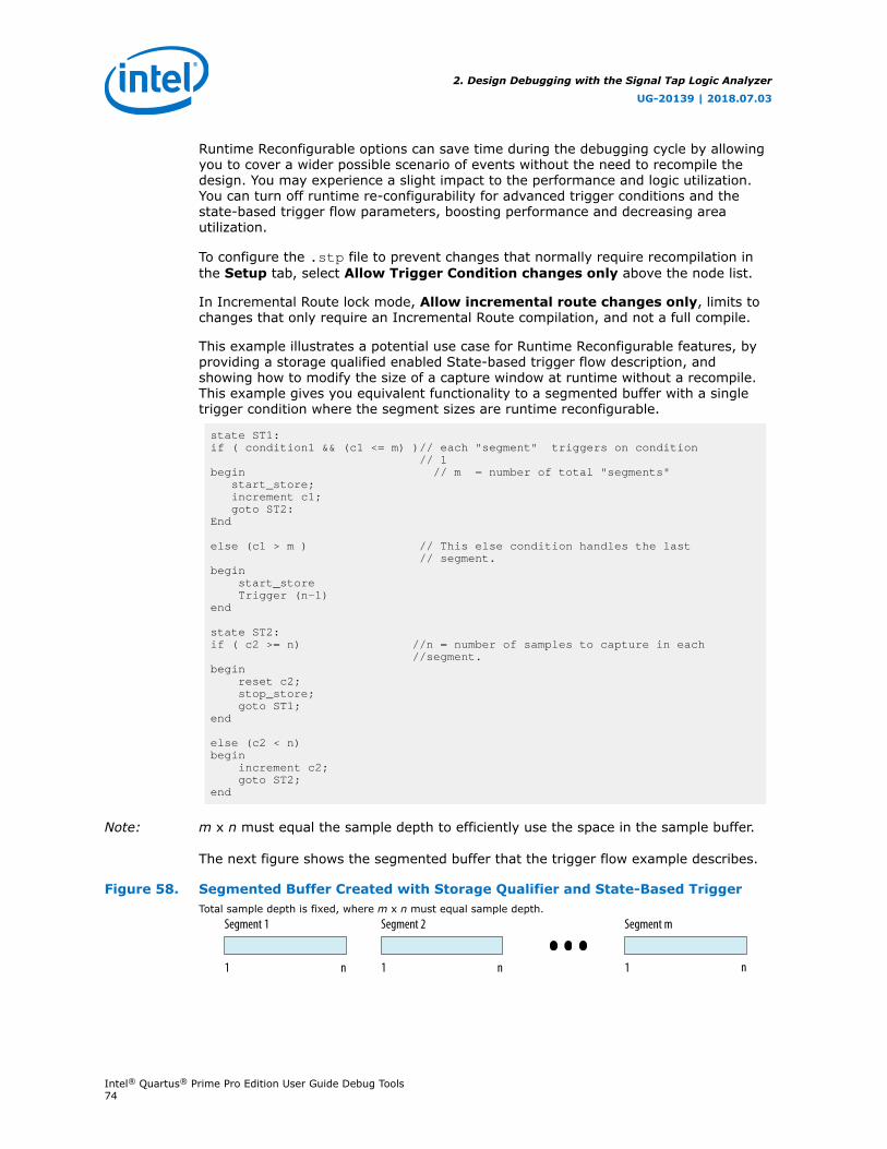
Runtime Reconfigurable options can save time during the debugging cycle by allowingyou to cover a wider possible scenario of events without the need to recompile thedesign. You may experience a slight impact to the performance and logic utilization.You can turn off runtime re-configurability for advanced trigger conditions and thestate-based trigger flow parameters, boosting performance and decreasing areautilization.
To configure the .stp file to prevent changes that normally require recompilation inthe Setup tab, select Allow Trigger Condition changes only above the node list.
In Incremental Route lock mode, Allow incremental route changes only, limits tochanges that only require an Incremental Route compilation, and not a full compile.
This example illustrates a potential use case for Runtime Reconfigurable features, byproviding a storage qualified enabled State-based trigger flow description, andshowing how to modify the size of a capture window at runtime without a recompile.This example gives you equivalent functionality to a segmented buffer with a singletrigger condition where the segment sizes are runtime reconfigurable.
state ST1:if ( condition1 && (c1 <= m) )// each "segment" triggers on condition // 1begin // m = number of total "segments" start_store; increment c1; goto ST2:End
else (c1 > m ) // This else condition handles the last // segment.begin start_store Trigger (n-1)end
state ST2:if ( c2 >= n) //n = number of samples to capture in each //segment.begin reset c2; stop_store; goto ST1;end else (c2 < n)begin increment c2; goto ST2;end
Note: m x n must equal the sample depth to efficiently use the space in the sample buffer.
The next figure shows the segmented buffer that the trigger flow example describes.
Figure 58. Segmented Buffer Created with Storage Qualifier and State-Based TriggerTotal sample depth is fixed, where m x n must equal sample depth.
Segment 1
1 n
Segment 2
1 n
Segment m
1 n
2. Design Debugging with the Signal Tap Logic Analyzer
UG-20139 | 2018.07.03
Intel® Quartus® Prime Pro Edition User Guide Debug Tools74
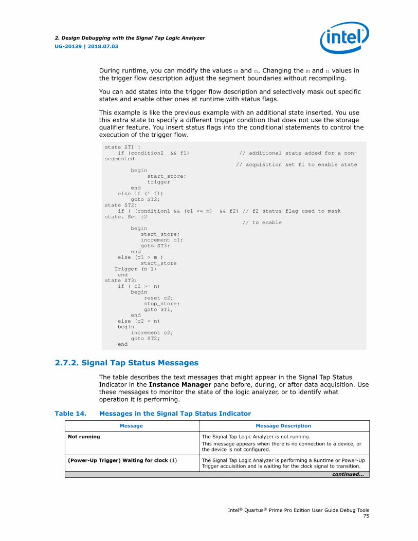
During runtime, you can modify the values m and n. Changing the m and n values inthe trigger flow description adjust the segment boundaries without recompiling.
You can add states into the trigger flow description and selectively mask out specificstates and enable other ones at runtime with status flags.
This example is like the previous example with an additional state inserted. You usethis extra state to specify a different trigger condition that does not use the storagequalifier feature. You insert status flags into the conditional statements to control theexecution of the trigger flow.
state ST1 : if (condition2 && f1) // additional state added for a non-segmented // acquisition set f1 to enable state begin start_store; trigger end else if (! f1) goto ST2;state ST2: if ( (condition1 && (c1 <= m) && f2) // f2 status flag used to mask state. Set f2 // to enable begin start_store; increment c1; goto ST3: end else (c1 > m ) start_store Trigger (n-1) endstate ST3: if ( c2 >= n) begin reset c2; stop_store; goto ST1; end else (c2 < n) begin increment c2; goto ST2; end
2.7.2. Signal Tap Status Messages
The table describes the text messages that might appear in the Signal Tap StatusIndicator in the Instance Manager pane before, during, or after data acquisition. Usethese messages to monitor the state of the logic analyzer, or to identify whatoperation it is performing.
Table 14. Messages in the Signal Tap Status Indicator
Message Message Description
Not running The Signal Tap Logic Analyzer is not running.This message appears when there is no connection to a device, orthe device is not configured.
(Power-Up Trigger) Waiting for clock (1) The Signal Tap Logic Analyzer is performing a Runtime or Power-UpTrigger acquisition and is waiting for the clock signal to transition.
continued...
2. Design Debugging with the Signal Tap Logic Analyzer
UG-20139 | 2018.07.03
Intel® Quartus® Prime Pro Edition User Guide Debug Tools75
Message Message Description
Acquiring (Power-Up) pre-trigger data (1) The trigger condition has not been evaluated yet.If the acquisition mode is non-segmented buffer and the storagequalifier type is continuous, the Signal Tap Logic Analyzer collects afull buffer of data.
Trigger In conditions met Trigger In condition has occurred. The Signal Tap Logic Analyzer iswaiting for the first trigger condition to occur.This message only appears when a Trigger In condition exists.
Waiting for (Power-up) trigger (1) The Signal Tap Logic Analyzer is waiting for the trigger event tooccur.
Trigger level <x> met Trigger condition x occurred. The Signal Tap Logic Analyzer iswaiting for condition x + 1 to occur.
Acquiring (power-up) post-trigger data (1) The entire trigger event occurred. The Signal Tap Logic Analyzer isacquiring the post-trigger data.You define the amount of post-trigger data to collect (between12%, 50%, and 88%) when you select the non-segmented bufferacquisition mode.
Offload acquired (Power-Up) data (1) Data is being transmitted to the Intel Quartus Prime softwarethrough the JTAG chain.
Ready to acquire The Signal Tap Logic Analyzer is waiting for you to initialize theanalyzer.
1. This message can appear for both Runtime and Power-Up Trigger events. When referring to a Power-Up Trigger, thetext in parentheses appears.
Note: In segmented acquisition mode, pre-trigger and post-trigger do not apply.
2.8. View, Analyze, and Use Captured Data
Use the Signal Tap Logic Analyzer interface to examine the data you capturedmanually or using a trigger, and use your findings to debug your design.
When in the Data view, you can use the drag-to-zoom feature by left-clicking toisolate the data of interest.
Related Information
• Monitoring Locations in Memory on page 111
• Read Information from In-System Memory Commands (Processing Menu)In Intel Quartus Prime Help
• Stop In-System Memory Analysis Command (Processing Menu)In Intel Quartus Prime Help
2.8.1. Capturing Data Using Segmented Buffers
Segmented Acquisition buffers allow you to perform multiple captures with a separatetrigger condition for each acquisition segment. This feature allows you to capture arecurring event or sequence of events that span over a long period time efficiently.
Each acquisition segment acts as a non-segmented buffer, continuously capturing datawhen it is activated. When you run an analysis with the segmented buffer optionenabled, the Signal Tap Logic Analyzer performs back-to-back data captures for each
2. Design Debugging with the Signal Tap Logic Analyzer
UG-20139 | 2018.07.03
Intel® Quartus® Prime Pro Edition User Guide Debug Tools76
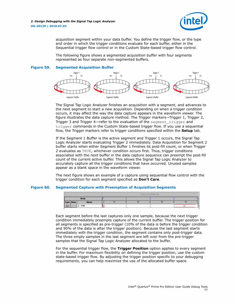
acquisition segment within your data buffer. You define the trigger flow, or the typeand order in which the trigger conditions evaluate for each buffer, either in theSequential trigger flow control or in the Custom State-based trigger flow control.
The following figure shows a segmented acquisition buffer with four segmentsrepresented as four separate non-segmented buffers.
Figure 59. Segmented Acquisition Buffer
0
1
1
Segment 1 Buffer
1
111
1
1
11
1 11
1
000
0
0
0
0 0
0
Trigger 1Post Pre
0
1
1
Segment 2 Buffer
1
111
1
1
11
1 11
1
000
0
0
0
0 0
0
Trigger 2Post Pre
0
1
1
Segment 3 Buffer
1
111
1
1
11
1 11
1
000
0
0
0
0 0
0
Trigger 3Post Pre
0
1
1
Segment 4 Buffer
1
111
1
1
11
1 11
1
000
0
0
0
0 0
0
Trigger 4Post Pre
The Signal Tap Logic Analyzer finishes an acquisition with a segment, and advances tothe next segment to start a new acquisition. Depending on when a trigger conditionoccurs, it may affect the way the data capture appears in the waveform viewer. Thefigure illustrates the data capture method. The Trigger markers—Trigger 1, Trigger 2,Trigger 3 and Trigger 4—refer to the evaluation of the segment_trigger andtrigger commands in the Custom State-based trigger flow. If you use a sequentialflow, the Trigger markers refer to trigger conditions specified within the Setup tab.
If the Segment 1 Buffer is the active segment and Trigger 1 occurs, the Signal TapLogic Analyzer starts evaluating Trigger 2 immediately. Data Acquisition for Segment 2buffer starts when either Segment Buffer 1 finishes its post-fill count, or when Trigger2 evaluates as TRUE, whichever condition occurs first. Thus, trigger conditionsassociated with the next buffer in the data capture sequence can preempt the post-fillcount of the current active buffer. This allows the Signal Tap Logic Analyzer toaccurately capture all the trigger conditions that have occurred. Unused samplesappear as a blank space in the waveform viewer.
The next figure shows an example of a capture using sequential flow control with thetrigger condition for each segment specified as Don’t Care.
Figure 60. Segmented Capture with Preemption of Acquisition Segments
Each segment before the last captures only one sample, because the next triggercondition immediately preempts capture of the current buffer. The trigger position forall segments is specified as pre-trigger (10% of the data is before the trigger conditionand 90% of the data is after the trigger position). Because the last segment startsimmediately with the trigger condition, the segment contains only post-trigger data.The three empty samples in the last segment are left over from the pre-triggersamples that the Signal Tap Logic Analyzer allocated to the buffer.
For the sequential trigger flow, the Trigger Position option applies to every segmentin the buffer. For maximum flexibility on defining the trigger position, use the customstate-based trigger flow. By adjusting the trigger position specific to your debuggingrequirements, you can help maximize the use of the allocated buffer space.
2. Design Debugging with the Signal Tap Logic Analyzer
UG-20139 | 2018.07.03
Intel® Quartus® Prime Pro Edition User Guide Debug Tools77

2.8.2. Differences in Pre-fill Write Behavior Between Different AcquisitionModes
The Signal Tap Logic Analyzer uses one of the following three modes when writing intothe acquisition memory:
• Non-segmented buffer
• Non-segmented buffer with a storage qualifier
• Segmented buffer
There are subtle differences in the amount of data captured immediately after runningthe Signal Tap Logic Analyzer and before any trigger conditions occur. A non-segmented buffer, running in continuous mode, completely fills the buffer withsampled data before evaluating any trigger conditions. Thus, a non-segmentedcapture without any storage qualification enabled always shows a waveform with a fullbuffer's worth of data captured.
Filling the buffer provides you with as much data as possible within the capturewindow. The buffer gets pre-filled with data samples prior to evaluating the triggercondition. As such, Signal Tap requires that the buffer be filled at least once beforeany data can be retrieved through the JTAG connection and prevents the buffer frombeing dumped during the first acquisition prior to a trigger condition when youperform a Stop Analysis.
For segmented buffers and non-segmented buffers using any storage qualificationmode, the Signal Tap Logic Analyzer immediately evaluates all trigger conditions whilewriting samples into the acquisition memory. This evaluation is especially importantwhen using any storage qualification on the data set. The logic analyzer may miss atrigger condition if it waits to capture a full buffer's worth of data before evaluatingany trigger conditions,
If the trigger event occurs on any data sample before the specified amount of pre-trigger data has occurred, then the Signal Tap Logic Analyzer triggers and beginsfilling memory with post-trigger data, regardless of the amount of pre-trigger data youspecify. For example, if you set the trigger position to 50% and set the logic analyzerto trigger on a processor reset, start the logic analyzer, and then power on your targetsystem, the logic analyzer triggers. However, the logic analyzer memory is filled onlywith post-trigger data, and not any pre-trigger data, because the trigger event, whichhas higher precedence than the capture of pre-trigger data, occurred before the pre-trigger condition was satisfied.
The figures for continuous data capture and conditional data capture show thedifference between a non-segmented buffer in continuous mode and a non-segmentedbuffer using a storage qualifier. The configuration of the logic analyzer waveformsbelow is a base trigger condition, sample depth of 64 bits, and Post trigger position.
Figure 61. Signal Tap Logic Analyzer Continuous Data Capture
2. Design Debugging with the Signal Tap Logic Analyzer
UG-20139 | 2018.07.03
Intel® Quartus® Prime Pro Edition User Guide Debug Tools78
In the continuous data capture, Trig1 occurs several times in the data buffer beforethe Signal Tap Logic Analyzer actually triggers. A full buffer's worth of data is capturedbefore the logic analyzer evaluates any trigger conditions. After the trigger conditionoccurs, the logic analyzer continues acquisition until it captures eight additionalsamples (12% of the buffer, as defined by the "post-trigger" position).
Figure 62. Signal Tap Logic Analyzer Conditional Data Capture
Note to figure:
1. Conditional capture, storage always enabled, post-fill count.
2. Signal Tap Logic Analyzer capture of a recurring pattern using a non-segmentedbuffer in conditional mode. The configuration of the logic analyzer is a basictrigger condition "Trig1" and sample depth of 64 bits. The Trigger in condition isDon't care, which means that every sample is captured.
In conditional capture the logic analyzer triggers immediately. As in continuouscapture, the logic analyzer completes the acquisition with eight samples, or 12% of64, the sample capacity of the acquisition buffer.
2.8.3. Creating Mnemonics for Bit Patterns
The mnemonic table feature allows you to assign a meaningful name to a set of bitpatterns, such as a bus. To create a mnemonic table, right-click in the Setup or Datatab of an .stp and click Mnemonic Table Setup. You create a mnemonic table byentering sets of bit patterns and specifying a label to represent each pattern. Onceyou have created a mnemonic table, assign the table to a group of signals. To assign amnemonic table, right-click on the group, click Bus Display Format and select thedesired mnemonic table.
You use the labels you create in a table in different ways on the Setup and Data tabs.On the Setup tab, you can create basic triggers with meaningful names by right-clicking an entry in the Trigger Conditions column and selecting a label from thetable you assigned to the signal group. On the Data tab, if any captured data matchesa bit pattern contained in an assigned mnemonic table, the signal group data isreplaced with the appropriate label, making it easy to see when expected datapatterns occur.
2.8.4. Automatic Mnemonics with a Plug-In
When you use a plug-in to add signals to an .stp, mnemonic tables for the addedsignals are automatically created and assigned to the signals defined in the plug-in. Toenable these mnemonic tables manually, right-click the name of the signal or signalgroup. On the Bus Display Format shortcut menu, then click the name of themnemonic table that matches the plug-in.
2. Design Debugging with the Signal Tap Logic Analyzer
UG-20139 | 2018.07.03
Intel® Quartus® Prime Pro Edition User Guide Debug Tools79
As an example, the Nios II plug-in helps you to monitor signal activity for your designas the code is executed. If you set up the logic analyzer to trigger on a function namein your Nios II code based on data from an .elf, you can see the function name inthe Instance Address signal group at the trigger sample, along with thecorresponding disassembled code in the Disassembly signal group, as shown in Figure 13–52. Captured data samples around the trigger are referenced as offsetaddresses from the trigger function name.
Figure 63. Data Tab when the Nios II Plug-In is Used
2.8.5. Locating a Node in the Design
When you find the source of an error in your design using the Signal Tap LogicAnalyzer, you can use the node locate feature to locate that signal in many of the toolsfound in the Intel Quartus Prime software, as well as in your design files. This lets youfind the source of the problem quickly so you can modify your design to correct theflaw. To locate a signal from the Signal Tap Logic Analyzer in one of the Intel QuartusPrime software tools or your design files, right-click the signal in the .stp, and clickLocate in <tool name>.
You can locate a signal from the node list with the following tools:
• Assignment Editor
• Pin Planner
• Timing Closure Floorplan
• Chip Planner
• Resource Property Editor
• Technology Map Viewer
• RTL Viewer
• Design File
2.8.6. Saving Captured Data
When you save a data capture, Signal Tap Logic Analyzer stores this data in theactive .stp file, and the Data Log adds the capture as a log entry under the currentconfiguration.
When analysis is set to Auto-run mode, the Logic Analyzer creates a separate entryin the Data Log to store the data captured each time the trigger occurred. This allowsyou to review the captured data for each trigger event.
The default name for a log is based time stamp when the Logic Analyzer acquired thedata. As a best practice, rename the data log with a more meaningful name.
2. Design Debugging with the Signal Tap Logic Analyzer
UG-20139 | 2018.07.03
Intel® Quartus® Prime Pro Edition User Guide Debug Tools80
The organization of logs is hierarchical; the Logic Analyzer groups similar logs ofcaptured data in trigger sets.
Related Information
Data Log Pane on page 42
2.8.7. Exporting Captured Data to Other File Formats
You can export captured data to the following file formats, for use with other EDAsimulation tools:
• Comma Separated Values File (.csv)
• Table File (.tbl)
• Value Change Dump File (.vcd)
• Vector Waveform File (.vwf)
• Graphics format files (.jpg, .bmp)
To export the captured data from Signal Tap Logic Analyzer, on the File menu, clickExport and specify the File Name, Export Format, and Clock Period.
2.8.8. Creating a Signal Tap List File
A .stp list file contains all the data the logic analyzer captures for a trigger event, intext format.
Each row of the list file corresponds to one captured sample in the buffer. Columnscorrespond to the value of each of the captured signals or signal groups for thatsample. If you defined a mnemonic table for the captured data, a matching entry fromthe table replaces the numerical values in the list.
The .stp list file is especially useful when combined with a plug-in that includesinstruction code disassembly. You can view the order of instruction code executionduring the same time period of the trigger event.
To create a .stp list file in the Intel Quartus Prime software, click File ➤ Create/Update ➤ Create Signal Tap List File.
Related Information
Adding Signals with a Plug-In on page 31
2.9. Debugging Partial Reconfiguration Designs Using Signal TapLogic Analyzer
You can debug a PR design with Signal Tap. The PR support in the Signal Tap LogicAnalyzer includes data acquisition in static and PR regions. Moreover, you can debugmultiple personas present in a PR region and multiple PR regions.
2.9.1. Recommendations when Debugging PR Designs
Follow these guidelines to obtain best results when debugging PR Designs with theSignal Tap Logic Analyzer:
2. Design Debugging with the Signal Tap Logic Analyzer
UG-20139 | 2018.07.03
Intel® Quartus® Prime Pro Edition User Guide Debug Tools81

• Include the Signal Tap .stp file only in the PR synthesis revisions, or the baserevision compile. Do not include the .stp file in the implementation revisions.
• Include one .stp file per revision.
• Tap pre-synthesis nodes only. In the Node Finder, filter by Signal Tap: pre-synthesis.
• Do not tap nodes in the default personas (the personas you use in the baserevision compile). Create a new PR implementation revision that instantiates thedefault persona, and tap nodes in the new revision.
• Store all the tapped nodes from a PR persona in one .stp file, to enabledebugging the entire persona using only one Signal Tap window.
• Do not tap across PR regions, or from a static region to a PR region in thesame .stp file.
• Each Signal Tap window opens only one .stp file. Therefore, to debug more thanone partition simultaneously, open stand-alone Signal Tap windows from thecommand-line.
Related Information
Creating a Partial Reconfiguration Design
2.9.2. Setting Up a Partial Reconfiguration Design for Debug
To debug a PR design you must instantiate SLD JTAG bridges when generating thebase revision, and then define debug components for all PR personas. Optionally, youcan specify signals to tap in the static region.
Figure 64. Setting Up PR Design for Debug with Signal Tap
Prepare Base Revision
Finish
Start
Debug Static Region
Prepare PR Personas
Prepare Static Region
yes
no
After configuring all the PR personas in the design, you can continue the PR designflow.
Related Information
• Debug Fabric for Partial Reconfiguration Designs on page 16
• Partial Reconfiguration Design Flow
2. Design Debugging with the Signal Tap Logic Analyzer
UG-20139 | 2018.07.03
Intel® Quartus® Prime Pro Edition User Guide Debug Tools82

2.9.2.1. Prepare Static Region for Debug
To debug the static region in your PR design:
1. Tap nodes in the static region exclusively.
2. Save the .stp file. Use a name that identifies the file with the static region.
3. Enable Signal Tap in your project, and include the .stp file in the base revision.
Note: Do not tap signals in the default PR personas.
Related Information
Adding Signals to the Signal Tap File on page 28
2.9.2.2. Prepare Base Revision for Debug
In the base revision, for each PR region that you want to debug in the design:
1. Instantiate the SLD JTAG Bridge Agent IP in the static region.
2. Instantiate the SLD JTAG Bridge Host IP in the PR region of the default persona.
You can use the IP Catalog or Platform Designer to instantiate SLD JTAG Bridgecomponents.
Related Information
• Instantiating the SLD JTAG Bridge Agent on page 18
• Instantiating the SLD JTAG Bridge Host on page 19
2.9.2.3. Prepare PR Personas for Debug
Before you create revisions for personas in your design, you must instantiate debug IPcomponents and tap signals.
For each PR persona that you want to debug:
1. Instantiate the SLD JTAG bridge host in the PR persona.
2. Tap pre-synthesis nodes in the PR persona only. Use the PR synthesis revision.
3. Save in a new .stp file. Select a name that identifies the persona.
4. Use the new .stp file in the synthesis revision. Do not use a .stp file in theimplementation revision for the persona.
If you do not want to debug a particular persona, drive the tdo output signal to 0.
Related Information
• Instantiating the SLD JTAG Bridge Host on page 19
• Adding Signals to the Signal Tap File on page 28
2.9.3. Performing Data Acquisition in a PR design
After generating the .sof and .rbf files for the revisions you want to debug, you areready to program your device and debug with the Signal Tap Logic Analyzer.
2. Design Debugging with the Signal Tap Logic Analyzer
UG-20139 | 2018.07.03
Intel® Quartus® Prime Pro Edition User Guide Debug Tools83

To perform data acquisition:
1. Program the base image into your device.
2. Partially reconfigure the device into the implementation you want to debug.
3. Open the Signal Tap Logic Analyzer by clicking Tools ➤ Signal Tap LogicAnalyzer in the Intel Quartus Prime software.
The Logic Analyzer opens and loads the .stp file set in the current active revision.
4. To debug other regions in your design, open new Signal Tap windows by openingthe other region's .stp file from the Intel Quartus Prime main window.
Alternatively, use the command-line:
quartus_stpw <stp_file_other_region.stp>
5. Debug your design with Signal Tap.
To debug another revision, you must partially reconfigure your design with thecorresponding .rbf file.
Related Information
• Program the Target Device or Devices on page 71
• Running the Signal Tap Logic Analyzer on page 72
• View, Analyze, and Use Captured Data on page 76
2.10. Other Features
The Signal Tap Logic Analyzer provides optional features not specific to a task flow.The following techniques can offer advantages in specific scenarios.
2.10.1. Creating Signal Tap File from Design Instances
In addition to providing GUI support for generation of .stp files, the Intel QuartusPrime software supports generation of a Signal Tap instance from logic defined in HDLsource files. This technique is helpful to modify runtime configurable triggerconditions, acquire data, and view acquired data on the data log via Signal Taputilities.
2.10.1.1. Creating a .stp File from a Design Instance
To generate a .stp file from parameterized HDL instances within your design:
1. Open or create an Intel Quartus Prime project that includes one or more HDLinstances of the Signal Tap logic analyzer.
2. Click Processing ➤ Start ➤ Start Analysis & Synthesis.
3. Click File ➤ Create/Update ➤ Create Signal Tap File from DesignInstance(s).
4. Specify a location for the .stp file that generates, and click Save.
2. Design Debugging with the Signal Tap Logic Analyzer
UG-20139 | 2018.07.03
Intel® Quartus® Prime Pro Edition User Guide Debug Tools84
Figure 65. Create Signal Tap File from Design Instances Dialog Box
Note: If your project contains partial reconfiguration partitions, the Create SignalTap File from Design Instance(s) dialog box displays a tree view of thePR partitions in the project. Select a partition from the view, and clickCreate Signal Tap file. The resultant .stp file that generates contains allHDL instances in the corresponding PR partition. The resultant .stp filedoes not include the instances in any nested partial reconfigurationpartition.
Figure 66. Selecting Partition for .stp File Generation
After successful .stp file creation, the Signal Tap Logic Analyzer appears. All thefields are read-only, except runtime-configurable trigger conditions.
2. Design Debugging with the Signal Tap Logic Analyzer
UG-20139 | 2018.07.03
Intel® Quartus® Prime Pro Edition User Guide Debug Tools85
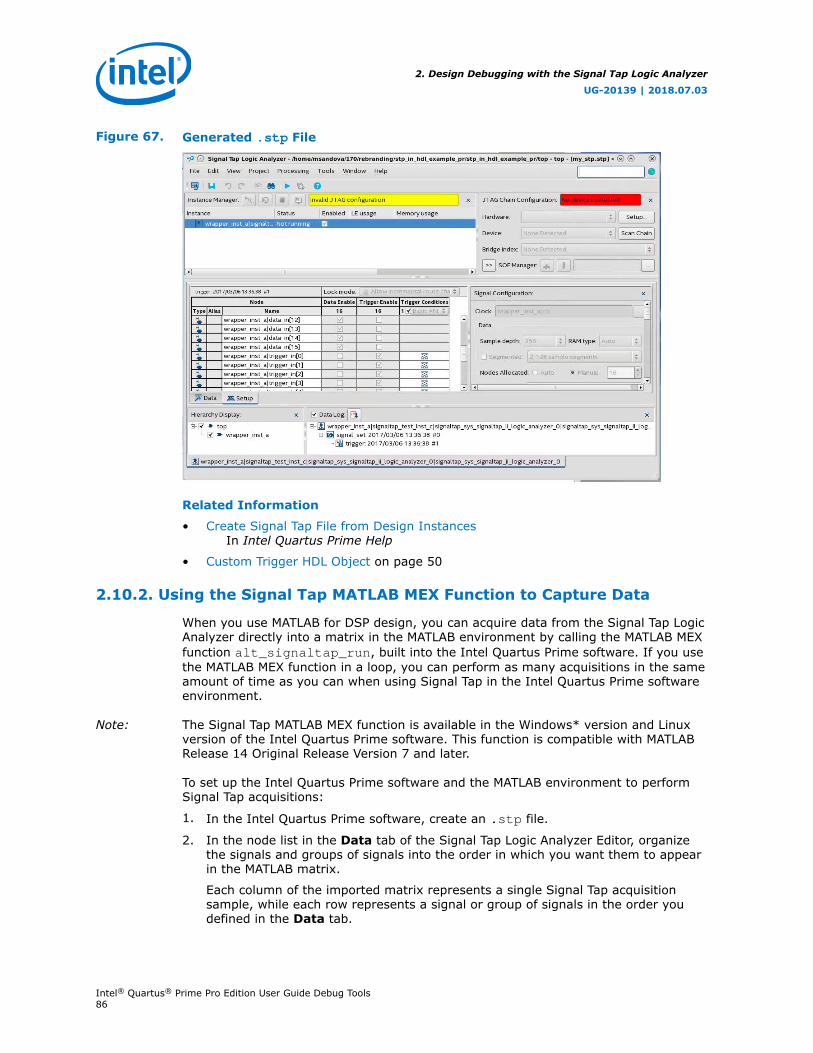
Figure 67. Generated .stp File
Related Information
• Create Signal Tap File from Design InstancesIn Intel Quartus Prime Help
• Custom Trigger HDL Object on page 50
2.10.2. Using the Signal Tap MATLAB MEX Function to Capture Data
When you use MATLAB for DSP design, you can acquire data from the Signal Tap LogicAnalyzer directly into a matrix in the MATLAB environment by calling the MATLAB MEXfunction alt_signaltap_run, built into the Intel Quartus Prime software. If you usethe MATLAB MEX function in a loop, you can perform as many acquisitions in the sameamount of time as you can when using Signal Tap in the Intel Quartus Prime softwareenvironment.
Note: The Signal Tap MATLAB MEX function is available in the Windows* version and Linuxversion of the Intel Quartus Prime software. This function is compatible with MATLABRelease 14 Original Release Version 7 and later.
To set up the Intel Quartus Prime software and the MATLAB environment to performSignal Tap acquisitions:
1. In the Intel Quartus Prime software, create an .stp file.
2. In the node list in the Data tab of the Signal Tap Logic Analyzer Editor, organizethe signals and groups of signals into the order in which you want them to appearin the MATLAB matrix.
Each column of the imported matrix represents a single Signal Tap acquisitionsample, while each row represents a signal or group of signals in the order youdefined in the Data tab.
2. Design Debugging with the Signal Tap Logic Analyzer
UG-20139 | 2018.07.03
Intel® Quartus® Prime Pro Edition User Guide Debug Tools86
Note: Signal groups that the Signal Tap Logic Analyzer acquires and transfers intothe MATLAB MEX function have a width limit of 32 signals. To use theMATLAB MEX function with a bus or signal group that contains more than 32signals, split the group into smaller groups that do not exceed the limit.
3. Save the .stp file and compile your design. Program your device and run theSignal Tap Logic Analyzer to ensure your trigger conditions and signal acquisitionwork correctly.
4. In the MATLAB environment, add the Intel Quartus Prime binary directory to yourpath with the following command:
addpath <Quartus install directory>\win
You can view the help file for the MEX function by entering the following commandin MATLAB without any operators:
alt_signaltap_run
5. Use the MATLAB MEX function to open the JTAG connection to the device and runthe Signal Tap Logic Analyzer to acquire data. When you finish acquiring data,close the JTAG connection.
To open the JTAG connection and begin acquiring captured data directly into aMATLAB matrix called stp, use the following command:
stp = alt_signaltap_run \('<stp filename>'[,('signed'|'unsigned')[,'<instance names>'[, \'<signalset name>'[,'<trigger name>']]]]);
When capturing data, you must assign a filename, for example, <stp filename> asa requirement of the MATLAB MEX function. Other MATLAB MEX function optionsare described in the table:
Table 15. Signal Tap MATLAB MEX Function Options
Option Usage Description
signed
unsigned
'signed'
'unsigned'
The signed option turns signal group data into 32-bit two’s-complement signed integers. The MSB of the group asdefined in the Signal Tap Data tab is the sign bit. Theunsigned option keeps the data as an unsigned integer.The default is signed.
<instance name> 'auto_signaltap_0' Specify a Signal Tap instance if more than one instance isdefined. The default is the first instance in the .stp,auto_signaltap_0.
<signal set name><trigger name>
'my_signalset'
'my_trigger'
Specify the signal set and trigger from the Signal Tap datalog if multiple configurations are present in the .stp. Thedefault is the active signal set and trigger in the file.
During data acquisition, you can enable or disable verbose mode to see the statusof the logic analyzer. To enable or disable verbose mode, use the followingcommands:
alt_signaltap_run('VERBOSE_ON');-alt_signaltap_run('VERBOSE_OFF');
When you finish acquiring data, close the JTAG connection with the followingcommand:
alt_signaltap_run('END_CONNECTION');
2. Design Debugging with the Signal Tap Logic Analyzer
UG-20139 | 2018.07.03
Intel® Quartus® Prime Pro Edition User Guide Debug Tools87
For more information about the use of MATLAB MEX functions in MATLAB, refer tothe MATLAB Help.
2.10.3. Using Signal Tap in a Lab Environment
You can install a stand-alone version of the Signal Tap Logic Analyzer. This version isparticularly useful in a lab environment in which you do not have a workstation thatmeets the requirements for a complete Intel Quartus Prime installation, or if you donot have a license for a full installation of the Intel Quartus Prime software. Thestandalone version of the Signal Tap Logic Analyzer is included with and requires theIntel Quartus Prime stand-alone Programmer which is available from the Downloadspage of the Altera website.
2.10.4. Remote Debugging Using the Signal Tap Logic Analyzer
2.10.4.1. Debugging Using a Local PC and an SoC
You can use the System Console with Signal Tap Logic Analyzer to remote debug yourIntel FPGA SoC. This method requires one local PC, an existing TCP/IP connection, aprogramming device at the remote location, and an Intel FPGA SoC.
Related Information
Remote Hardware Debugging over TCP/IP
2.10.4.2. Debugging Using a Local PC and a Remote PC
You can use the Signal Tap Logic Analyzer to debug a design that is running on adevice attached to a PC in a remote location.
To perform a remote debugging session, you must have the following setup:
• The Intel Quartus Prime software installed on the local PC
• Stand-alone Signal Tap Logic Analyzer or the full version of the Intel QuartusPrime software installed on the remote PC
• Programming hardware connected to the device on the PCB at the remote location
• TCP/IP protocol connection
2.10.4.2.1. Equipment Setup
1. On the PC in the remote location, install the standalone version of the Signal TapLogic Analyzer, included in the Intel Quartus Prime stand-alone Programmer, orthe full version of the Intel Quartus Prime software.
2. Connect the remote computer to Intel programming hardware, such as the or IntelFPGA Download Cable.
3. On the local PC, install the full version of the Intel Quartus Prime software.
4. Connect the local PC to the remote PC across a LAN with the TCP/IP protocol.
2. Design Debugging with the Signal Tap Logic Analyzer
UG-20139 | 2018.07.03
Intel® Quartus® Prime Pro Edition User Guide Debug Tools88
2.10.5. Using the Signal Tap Logic Analyzer in Devices with ConfigurationBitstream Security
Certain device families support bitstream decryption during configuration using an on-device AES decryption engine. You can still use the Signal Tap Logic Analyzer toanalyze functional data within the FPGA. However, note that JTAG configuration is notpossible after the security key has been programmed into the device.
Intel FPGA recommends that you use an unencrypted bitstream during the prototypeand debugging phases of the design. Using an unencrypted bitstream allows you togenerate new programming files and reconfigure the device over the JTAG connectionduring the debugging cycle.
If you must use the Signal Tap Logic Analyzer with an encrypted bitstream, firstconfigure the device with an encrypted configuration file using Passive Serial (PS),Fast Passive Parallel (FPP), or Active Serial (AS) configuration modes. The design mustcontain at least one instance of the Signal Tap Logic Analyzer. After the FPGA isconfigured with a Signal Tap Logic Analyzer instance in the design, when you open theSignal Tap Logic Analyzer in the Intel Quartus Prime software, you then scan the chainand are ready to acquire data with the JTAG connection.
2.10.6. Monitor FPGA Resources Used by the Signal Tap Logic Analyzer
The Signal Tap Logic Analyzer has a built-in resource estimator that calculates thelogic resources and amount of memory that each logic analyzer instance uses.Furthermore, because the most demanding on-chip resource for the logic analyzer ismemory usage, the resource estimator reports the ratio of total RAM usage in yourdesign to the total amount of RAM available, given the results of the last compilation.The resource estimator provides a warning if a potential for a “no-fit” occurs.
You can see resource usage (by instance and total) in the columns of the InstanceManager pane of the Signal Tap Logic Analyzer Editor. Use this feature when youknow that your design is running low on resources.
The logic element value that the resource usage estimator reports may vary by asmuch as 10% from the actual resource usage.
2.11. Design Example: Using Signal Tap Logic Analyzers
The system in this example contains many components, including a Nios processor, adirect memory access (DMA) controller, on-chip memory, and an interface to externalSDRAM memory. After you press a button, the processor initiates a DMA transfer,which you analyze using the Signal Tap Logic Analyzer. In this example, the Niosprocessor executes a simple C program from on-chip memory and waits for you topress a button.
Related Information
AN 446: Debugging Nios II Systems with the Signal Tap Embedded Logic Analyzerapplication note
2. Design Debugging with the Signal Tap Logic Analyzer
UG-20139 | 2018.07.03
Intel® Quartus® Prime Pro Edition User Guide Debug Tools89
2.12. Custom Triggering Flow Application Examples
The custom triggering flow in the Signal Tap Logic Analyzer is most useful fororganizing a number of triggering conditions and for precise control over theacquisition buffer. This section provides two application examples for defining acustom triggering flow within the Signal Tap Logic Analyzer. Both examples can beeasily copied and pasted directly into the state machine description box by using thestate display mode All states in one window.
Related Information
On-chip Debugging Design Examples website
2.12.1. Design Example 1: Specifying a Custom Trigger Position
Actions to the acquisition buffer can accept an optional post-count argument. Thispost-count argument enables you to define a custom triggering position for eachsegment in the acquisition buffer.
The example shows how to apply a trigger position to all segments in the acquisitionbuffer. The example describes a triggering flow for an acquisition buffer split into foursegments. If each acquisition segment is 64 samples in depth, the trigger position foreach buffer is at sample #34. The acquisition stops after all segments are filled once.
if (c1 == 3 && condition1) trigger 30;else if ( condition1 )begin segment_trigger 30; increment c1;end
Each segment acts as a non-segmented buffer that continuously updates the memorycontents with the signal values.
The Data tab displays the last acquisition before stopping the buffer as the lastsample number in the affected segment. The trigger position in the affected segmentis then defined by N – post count fill, where N is the number of samples persegment.
2. Design Debugging with the Signal Tap Logic Analyzer
UG-20139 | 2018.07.03
Intel® Quartus® Prime Pro Edition User Guide Debug Tools90
Figure 68. Specifying a Custom Trigger Position
0
1
1
111
1
1
11
1 11
1
1
000
0
0
0
0 0
0
Trigger
Sample #1
Post Count
Last Sample
2.12.2. Design Example 2: Trigger When triggercond1 Occurs Ten Timesbetween triggercond2 and triggercond3
The custom trigger flow description is often useful to count a sequence of eventsbefore triggering the acquisition buffer. The example shows such a sample flow. Thisexample uses three basic triggering conditions configured in the Signal Tap Setup tab.
This example triggers the acquisition buffer when condition1 occurs aftercondition3 and occurs ten times prior to condition3. If condition3 occurs priorto ten repetitions of condition1, the state machine transitions to a permanent waitstate.
state ST1:if ( condition2 )begin reset c1; goto ST2;endState ST2 :if ( condition1 ) increment c1;else if (condition3 && c1 < 10) goto ST3;else if ( condition3 && c1 >= 10) trigger;ST3:goto ST3;
2.13. Signal Tap Scripting Support
The Intel Quartus Prime supports automating Signal Tap procedures in a scriptingenvironment, as Tcl scripts or through the quartus_stp executable.
2. Design Debugging with the Signal Tap Logic Analyzer
UG-20139 | 2018.07.03
Intel® Quartus® Prime Pro Edition User Guide Debug Tools91
For detailed information about scripting command options, refer to the Intel QuartusPrime Command-Line and Tcl API Help browser. To run the Help browser, typequartus_sh --qhelp at the command prompt.
Related Information
Tcl Scripting
2.13.1. Signal Tap Command-Line Options
You can use the following options with the quartus_stp executable:
Table 16. quartus_stp Command-Line Options
Option Usage Description
--stp_file <stp_filename> Required Specifies the name of the .stp file.
--enable Optional Sets the ENABLE_SIGNALTAP option to ON in the project's .qsf file, sothe Signal Tap Logic Analyzer runs in the next compilation.If you omit this option, the Intel Quartus Prime software uses the currentvalue of ENABLE_SIGNALTAP in the .qsf file.Writes subsequent Signal Tap assignments to the .stp that appears inthe .qsf file. If the .qsf file does not specify a .stp file, you must usethe --stp_file option.
--disable Optional Sets the ENABLE_SIGNALTAP option to OFF in the project's .qsf file, sothe Signal Tap Logic Analyzer does not in the next compilation.If you omit the --disable option, the Intel Quartus Prime softwareuses the current value of ENABLE_SIGNALTAP in the .qsf file.
2.13.2. Data Capture from the Command Line
The quartus_stp executable supports a Tcl interface that allows you to capture datawithout running the Intel Quartus Prime GUI.
Note: You cannot execute Signal Tap Tcl commands from within the Tcl console in the IntelQuartus Prime software.
To execute a Tcl script containing Signal Tap Logic Analyzer Tcl commands, use:
quartus_stp -t <Tcl file>
Example 5. Continuously Capturing Data
This excerpt shows commands you can use to continuously capture data. Once thecapture meets trigger condition e, the Signal Tap Logic Analyzer starts the capture andstores the data in the data log.
# Open Signal Tap sessionopen_session -name stp1.stp
### Start acquisition of instances auto_signaltap_0 and### auto_signaltap_1 at the same time
# Calling run_multiple_end starts all instancesrun_multiple_start
run -instance auto_signaltap_0 -signal_set signal_set_1 -trigger \trigger_1 -data_log log_1 -timeout 5run -instance auto_signaltap_1 -signal_set signal_set_1 -trigger \
2. Design Debugging with the Signal Tap Logic Analyzer
UG-20139 | 2018.07.03
Intel® Quartus® Prime Pro Edition User Guide Debug Tools92

trigger_1 -data_log log_1 -timeout 5
run_multiple_end
# Close Signal Tap sessionclose_session
Related Information
::quartus::stpIn Intel Quartus Prime Help
2.14. Design Debugging with the Signal Tap Logic Analyzer RevisionHistory
Document Version Intel QuartusPrime Version
Changes
2018.05.07 18.0.0 • Added note stating Signal Tap IP not optimized for Stratix 10 Devices.• Moved information about debug fabric on PR designs to the System
Debugging Tools Overview chapter.• Removed restrictions of Rapid Recompile support for Intel Stratix 10
devices.
2017.11.06 17.1.0 • Added support for Incremental Routing in Intel Stratix 10 devices.• Removed unsupported FSM auto detection.• Clarified information about the Data Log Pane.• Updated Figure: Data Log and renamed to Simple Data Log.• Added Figure: Accessing the Advanced Trigger Condition Tab.• Removed outdated information about command-line flow.
2017.05.08 17.0.0 • Added: Open Standalone Signal Tap Logic Analyzer GUI.• Added: Debugging Partial Reconfiguration Designs Using Signal Tap
Logic Analyzer.• Updated figures on Create Signal Tap File from Design Instance(s).
2016.10.31 16.1.0 • Implemented Intel rebranding.• Added: Create Signal Tap File from Design Instance(s).• Removed reference to unsupported Talkback feature.
2016.05.03 16.0.0 • Added: Specifying the Pipeline Factor• Added: Comparison Trigger Conditions
2015.11.02 15.1.0 • Changed instances of Quartus II to Intel Quartus Prime.• Updated content to reflect Signal Tap support in Intel Quartus Prime
Pro Edition
2015.05.04 15.0.0 Added content for Floating Point Display Format in table: Signal Tap LogicAnalyzer Features and Benefits.
2014.12.15 14.1.0 Updated location of Fitter Settings, Analysis & Synthesis Settings, andPhysical Synthesis Optimizations to Compiler Settings.
December 2014 14.1.0 • Added MAX 10 as supported device.• Removed Full Incremental Compilation setting and Post-Fit (Strict)
netlist type setting information.• Removed outdated GUI images from "Using Incremental Compilation
with the Signal Tap Logic Analyzer" section.
continued...
2. Design Debugging with the Signal Tap Logic Analyzer
UG-20139 | 2018.07.03
Intel® Quartus® Prime Pro Edition User Guide Debug Tools93
Document Version Intel QuartusPrime Version
Changes
June 2014 14.0.0 • DITA conversion.• Replaced MegaWizard Plug-In Manager and Megafunction content with
IP Catalog and parameter editor content.• Added flows for custom trigger HDL object, Incremental Route with
Rapid Recompile, and nested groups with Basic OR.• GUI changes: toolbar, drag to zoom, disable/enable instance, trigger
log time-stamping.
November 2013 13.1.0 Removed HardCopy material. Added section on using cross-triggering withDS-5 tool and added link to white paper 01198. Added section on remotedebugging an Altera SoC and added link to application note 693. Updatedsupport for MEX function.
May 2013 13.0.0 • Added recommendation to use the state-based flow for segmentedbuffers with separate trigger conditions, information about Basic ORtrigger condition, and hard processor system (HPS) external triggers.
• Updated “Segmented Buffer” on page 13-17, Conditional Mode on page13-21, Creating Basic Trigger Conditions on page 13-16, and UsingExternal Triggers on page 13-48.
June 2012 12.0.0 Updated Figure 13–5 on page 13–16 and “Adding Signals to the Signal TapFile” on page 13–10.
November 2011 11.0.1 Template update.Minor editorial updates.
May 2011 11.0.0 Updated the requirement for the standalone Signal Tap software.
December 2010 10.0.1 Changed to new document template.
July 2010 10.0.0 • Add new acquisition buffer content to the “View, Analyze, and UseCaptured Data” section.
• Added script sample for generating hexadecimal CRC values inprogrammed devices.
• Created cross references to Intel Quartus Prime Help for duplicatedprocedural content.
November 2009 9.1.0 No change to content.
March 2009 9.0.0 • Updated Table 13–1• Updated “Using Incremental Compilation with the Signal Tap Logic
Analyzer” on page 13–45• Added new Figure 13–33• Made minor editorial updates
November 2008 8.1.0 Updated for the Intel Quartus Prime software version 8.1 release:• Added new section “Using the Storage Qualifier Feature” on page 14–
25• Added description of start_store and stop_store commands in
section “Trigger Condition Flow Control” on page 14–36• Added new section “Runtime Reconfigurable Options” on page 14–63
May 2008 8.0.0 Updated for the Intel Quartus Prime software version 8.0:• Added “Debugging Finite State machines” on page 14-24• Documented various GUI usability enhancements, including
improvements to the resource estimator, the bus find feature, and thedynamic display updates to the counter and flag resources in the State-based trigger flow control tab
• Added “Capturing Data Using Segmented Buffers” on page 14–16• Added hyperlinks to referenced documents throughout the chapter• Minor editorial updates
2. Design Debugging with the Signal Tap Logic Analyzer
UG-20139 | 2018.07.03
Intel® Quartus® Prime Pro Edition User Guide Debug Tools94

Related Information
Documentation ArchiveFor previous versions of the Intel Quartus Prime Handbook, search thedocumentation archives.
2. Design Debugging with the Signal Tap Logic Analyzer
UG-20139 | 2018.07.03
Intel® Quartus® Prime Pro Edition User Guide Debug Tools95
4. Quick Design Verification with Signal ProbeThis chapter showcases a debugging technique that provides early access to internaldevice signals without affecting the design.
The Signal Probe feature in the Intel Quartus Prime Pro Edition software allows you toroute an internal node to a top-level I/O. When you start with a fully routed design,you can select and route debugging signals to I/O pins that you previously reserve orare currently unused.
During Rapid Recompile, the Compiler reuses previous synthesis and fitting resultswhenever possible, and does not reprocess unchanged design blocks. When you makesmall design changes, using Rapid Recompile reduces timing variations and the totalrecompilation time.
The Intel Quartus Prime Pro Edition Signal Probe feature supports the Intel Arria 10and Intel Stratix 10 device families.
Related Information
System Debugging Tools Overview on page 7
4.1. Debug Flow with Signal Probe and Rapid Recompile
To add verification capabilities to a design using Signal Probe routing feature:
Reserve Signal Probe Pins on page 96
Compile the Design on page 97
Assign Nodes to Signal Probe Pins on page 97
Recompile the Design on page 97
Check Connection Table in Fitter Report on page 98
4.1.1. Reserve Signal Probe Pins
You create and reserve a pin for Signal Probe with a Tcl command:
set_global_assignment –name CREATE_SIGNALPROBE_PIN <pin_name>
pin_name Specifies the name of the Signal Probe pin.
Optionally, you can assign locations for the Signal Probe pins. If you do not assign alocation, the Fitter places the pins automatically.
Note: If from the onset of the debugging process you know which internal signals you wantto route, you can reserve pins and assign nodes before compilation. This earlyassignment removes the recompilation step from the flow.
UG-20139 | 2018.07.03
Intel Corporation. All rights reserved. Intel, the Intel logo, Altera, Arria, Cyclone, Enpirion, MAX, Nios, Quartusand Stratix words and logos are trademarks of Intel Corporation or its subsidiaries in the U.S. and/or othercountries. Intel warrants performance of its FPGA and semiconductor products to current specifications inaccordance with Intel's standard warranty, but reserves the right to make changes to any products and servicesat any time without notice. Intel assumes no responsibility or liability arising out of the application or use of anyinformation, product, or service described herein except as expressly agreed to in writing by Intel. Intelcustomers are advised to obtain the latest version of device specifications before relying on any publishedinformation and before placing orders for products or services.*Other names and brands may be claimed as the property of others.
ISO9001:2008Registered

Example 6. Tcl Command to Reserve Signal Probe Pins
set_global_assignment -name CREATE_SIGNALPROBE_PIN wizardset_global_assignment -name CREATE_SIGNALPROBE_PIN probey
Related Information
Constraining Designs with Tcl ScriptsIn Design Constraints User Guide: Intel Quartus Prime Pro Edition
4.1.2. Compile the Design
Perform a full compilation of the design. You can use Intel Quartus Prime software, acommand line executable, or a Tcl command.
Example 7. Tcl Command to Compile the Design
execute_flow -compile
At this point in the design flow you determine the nodes you want to debug.
Related Information
Design CompilationIn Compiler User Guide: Intel Quartus Prime Pro Edition
4.1.3. Assign Nodes to Signal Probe Pins
You can assign any node in the post-compilation netlist to a Signal Probe pin. In IntelQuartus Prime software, click View ➤ Node Finder, and filter by Signal Tap: post-fitting to view the nodes you can route.
You specify the node that connects to a Signal Probe pin with a Tcl command:
set_instance_assignment –name CONNECT_SIGNALPROBE_PIN <pin_name> –to <node_name>
pin_name Specifies the name of the Signal Probe pin that connects to the node.
node_name Specifies the full hierarchy path of the node you want to route.
Example 8. Tcl Commands to Connect Pins to Internal Nodes
# Make assignments to connect nodes of interest to pinsset_instance_assignment -name CONNECT_SIGNALPROBE_PIN wizard -to sprobe_me1set_instance_assignment -name CONNECT_SIGNALPROBE_PIN probey -to sprobe_me2
4.1.4. Recompile the Design
After assigning nodes to the Signal Probe pins, run Rapid Recompile. Rapid Recompilepreserves timing and reduces compilation time by reusing previous results wheneverpossible.
You can run Rapid Recompile from the Intel Quartus Prime software, a command lineexecutable, or a Tcl script.
4. Quick Design Verification with Signal Probe
UG-20139 | 2018.07.03
Intel® Quartus® Prime Pro Edition User Guide Debug Tools97
Example 9. Tcl Command to Recompile the Design
# Run the fitter with --recompile to preserve timing# and quickly connect the Signal Probe pinsexecute_module -tool fit -args {--recompile}
After recompilation, you are ready to program the device and debug the design.
Related Information
Using Rapid RecompileIn Compiler User Guide: Intel Quartus Prime Pro Edition
4.1.5. Check Connection Table in Fitter Report
When you compile a design with Signal Probe pins, Intel Quartus Prime softwaregenerates a connection report table. To see this report, click Processing ➤Compilation Report, open the Fitter ➤ In-System Debugging folder, and clickConnections to Signal Probe pins.
The Status column informs whether or not the routing attempt from the nodes to theSignal Probe pins succeeded.
Table 17. Status of Signal Probe Connection
Status Description
Connected Routing succeeded.
Unconnected Routing did not succeed. Possible reasons are:• Node belongs to an IO cell or another hard IP, thus cannot be routed.• Node hierarchy path does not exist in the design.• Node is not Signal Tap: post-fitting.
Example 10. Connections to Signal Probe Pins in the Compilation Report
Alternatively, you can find the Signal Probe connection information in the Fitter reportfile (<project_name>.fit.rpt).
Example 11. Connections to Signal Probe Pins in top.fit.rpt
+--------------------------------------------------------------------------------+; Connections to Signal Probe pins ;+--------------------------------------------------------------------------------+Signal Probe Pin Name : probey
4. Quick Design Verification with Signal Probe
UG-20139 | 2018.07.03
Intel® Quartus® Prime Pro Edition User Guide Debug Tools98

Status : ConnectedAttempted Connection : sprobe_me2Actual Connection : sprobe_me2Details :
Signal Probe Pin Name : wizardStatus : ConnectedAttempted Connection : sprobe_me1Actual Connection : sprobe_me1Details :+--------------------------------------------------------------------------------+
Related Information
• Untappable Signals on page 30
• Text-Based Report FilesIn Scripting User Guide: Intel Quartus Prime Pro Edition
4.2. Quick Design Verification with Signal Probe Revision History
Document Version Intel QuartusPrime Version
Changes
2018.05.07 18.0.0 Initial release for Intel Quartus Prime Pro Edition software.
4. Quick Design Verification with Signal Probe
UG-20139 | 2018.07.03
Intel® Quartus® Prime Pro Edition User Guide Debug Tools99
5. In-System Debugging Using External Logic Analyzers
5.1. About the Intel Quartus Prime Logic Analyzer Interface
The Intel Quartus Prime Logic Analyzer Interface (LAI) allows you to use an externallogic analyzer and a minimal number of Intel-supported device I/O pins to examinethe behavior of internal signals while your design is running at full speed on yourIntel-supported device.
The LAI connects a large set of internal device signals to a small number of outputpins. You can connect these output pins to an external logic analyzer for debuggingpurposes. In the Intel Quartus Prime LAI, the internal signals are grouped together,distributed to a user-configurable multiplexer, and then output to available I/O pins onyour Intel-supported device. Instead of having a one-to-one relationship betweeninternal signals and output pins, the Intel Quartus Prime LAI enables you to map manyinternal signals to a smaller number of output pins. The exact number of internalsignals that you can map to an output pin varies based on the multiplexer settings inthe Intel Quartus Prime LAI.
Note: The term “logic analyzer” when used in this document includes both logic analyzersand oscilloscopes equipped with digital channels, commonly referred to as mixedsignal analyzers or MSOs.
The LAI does not support Hard Processor System (HPS) I/Os.
Related Information
Device Support Center
5.2. Choosing a Logic Analyzer
The Intel Quartus Prime software offers the following two general purpose on-chipdebugging tools for debugging a large set of RTL signals from your design:
• The Signal Tap Logic Analyzer
• An external logic analyzer, which connects to internal signals in your Intel-supported device by using the Intel Quartus Prime LAI
Table 18. Comparing the Signal Tap Logic Analyzer with the Logic Analyzer Interface
Feature Description Recommended LogicAnalyzer
Sample Depth You have access to a wider sample depth with anexternal logic analyzer. In the Signal Tap LogicAnalyzer, the maximum sample depth is set to
LAI
continued...
UG-20139 | 2018.07.03
Intel Corporation. All rights reserved. Intel, the Intel logo, Altera, Arria, Cyclone, Enpirion, MAX, Nios, Quartusand Stratix words and logos are trademarks of Intel Corporation or its subsidiaries in the U.S. and/or othercountries. Intel warrants performance of its FPGA and semiconductor products to current specifications inaccordance with Intel's standard warranty, but reserves the right to make changes to any products and servicesat any time without notice. Intel assumes no responsibility or liability arising out of the application or use of anyinformation, product, or service described herein except as expressly agreed to in writing by Intel. Intelcustomers are advised to obtain the latest version of device specifications before relying on any publishedinformation and before placing orders for products or services.*Other names and brands may be claimed as the property of others.
ISO9001:2008Registered
Feature Description Recommended LogicAnalyzer
128 Kb, which is a device constraint. However, withan external logic analyzer, there are no deviceconstraints, providing you a wider sample depth.
Debugging Timing Issues Using an external logic analyzer provides you withaccess to a “timing” mode, which enables you todebug combined streams of data.
LAI
Performance You frequently have limited routing resourcesavailable to place and route when you use the SignalTap Logic Analyzer with your design. An external logicanalyzer adds minimal logic, which removes resourcelimits on place-and-route.
LAI
Triggering Capability The Signal Tap Logic Analyzer offers triggeringcapabilities that are comparable to external logicanalyzers.
LAI or Signal Tap
Use of Output Pins Using the Signal Tap Logic Analyzer, no additionaloutput pins are required. Using an external logicanalyzer requires the use of additional output pins.
Signal Tap
Acquisition Speed With the Signal Tap Logic Analyzer, you can acquiredata at speeds of over 200 MHz. You can achieve thesame acquisition speeds with an external logicanalyzer; however, you must consider signal integrityissues.
Signal Tap
Related Information
System Debugging Tools Overview on page 7
5.2.1. Required Components
To perform analysis using the LAI you need the following components:
• Intel Quartus Prime software version 15.1 or later
• The device under test
• An external logic analyzer
• An Intel FPGA communications cable
• A cable to connect the Intel-supported device to the external logic analyzer
5. In-System Debugging Using External Logic Analyzers
UG-20139 | 2018.07.03
Intel® Quartus® Prime Pro Edition User Guide Debug Tools101
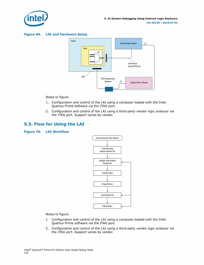
Figure 69. LAI and Hardware Setup
JTAG
(1)
(2)
FPGA
Connected toUnused FPGA Pins
LAI
FPGA ProgrammingHardware Quartus Prime Software
External Logic AnalyzerBoard
Notes to figure:
1. Configuration and control of the LAI using a computer loaded with the IntelQuartus Prime software via the JTAG port.
2. Configuration and control of the LAI using a third-party vendor logic analyzer viathe JTAG port. Support varies by vendor.
5.3. Flow for Using the LAI
Figure 70. LAI Workflow
Configure Logic AnalyzerInterface File
Create New LogicAnalyzer Interface File
Compile Project
Program Device
Control Output Pin
Debug Project
Start the Quartus Prime Software
Notes to figure:
1. Configuration and control of the LAI using a computer loaded with the IntelQuartus Prime software via the JTAG port.
2. Configuration and control of the LAI using a third-party vendor logic analyzer viathe JTAG port. Support varies by vendor.
5. In-System Debugging Using External Logic Analyzers
UG-20139 | 2018.07.03
Intel® Quartus® Prime Pro Edition User Guide Debug Tools102

5.3.1. Defining Parameters for the Logic Analyzer Interface
The Logic Analyzer Interface Editor allows you to define the parameters of the LAI.
• Click Tools ➤ Logic Analyzer Interface Editor.
Figure 71. Logic Analyzer Interface Editor
• In the Setup View list, select Core Parameters.
• Specify the parameters of the LAI instance.
Related Information
LAI Core Parameters on page 106
5.3.2. Mapping the LAI File Pins to Available I/O Pins
To assign pin locations for the LAI:
1. Select Pins in the Setup View list
5. In-System Debugging Using External Logic Analyzers
UG-20139 | 2018.07.03
Intel® Quartus® Prime Pro Edition User Guide Debug Tools103
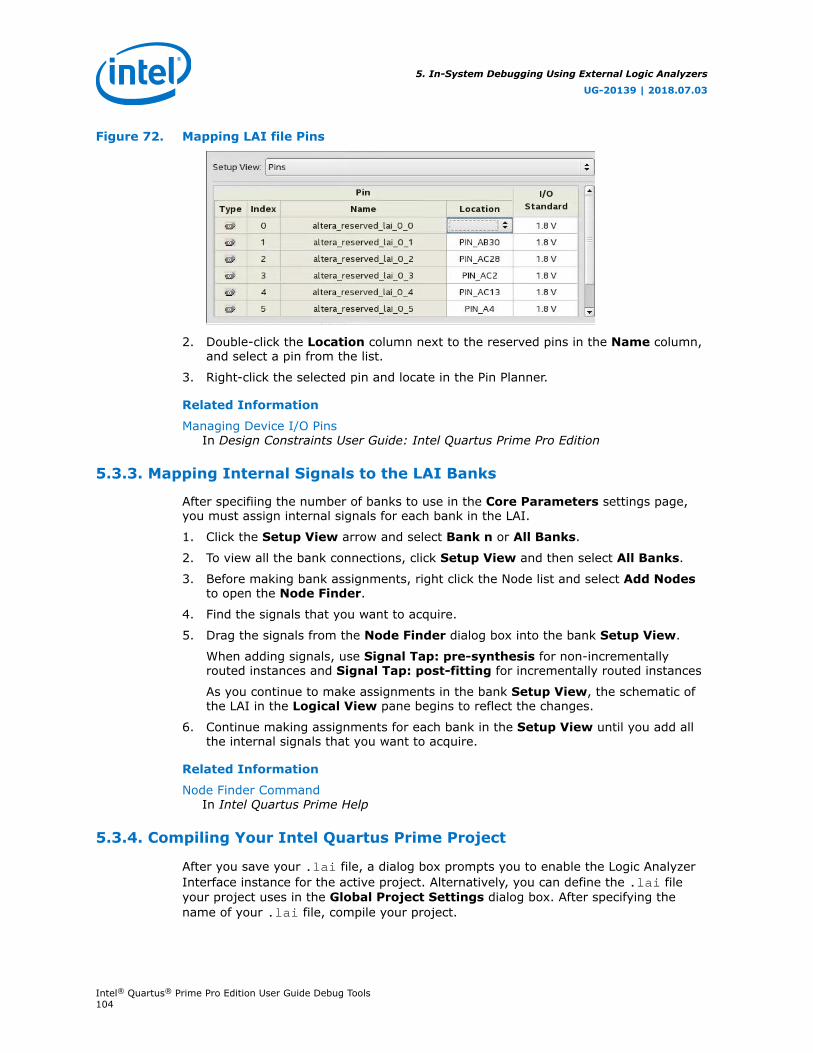
Figure 72. Mapping LAI file Pins
2. Double-click the Location column next to the reserved pins in the Name column,and select a pin from the list.
3. Right-click the selected pin and locate in the Pin Planner.
Related Information
Managing Device I/O PinsIn Design Constraints User Guide: Intel Quartus Prime Pro Edition
5.3.3. Mapping Internal Signals to the LAI Banks
After specifiing the number of banks to use in the Core Parameters settings page,you must assign internal signals for each bank in the LAI.
1. Click the Setup View arrow and select Bank n or All Banks.
2. To view all the bank connections, click Setup View and then select All Banks.
3. Before making bank assignments, right click the Node list and select Add Nodesto open the Node Finder.
4. Find the signals that you want to acquire.
5. Drag the signals from the Node Finder dialog box into the bank Setup View.
When adding signals, use Signal Tap: pre-synthesis for non-incrementallyrouted instances and Signal Tap: post-fitting for incrementally routed instances
As you continue to make assignments in the bank Setup View, the schematic ofthe LAI in the Logical View pane begins to reflect the changes.
6. Continue making assignments for each bank in the Setup View until you add allthe internal signals that you want to acquire.
Related Information
Node Finder CommandIn Intel Quartus Prime Help
5.3.4. Compiling Your Intel Quartus Prime Project
After you save your .lai file, a dialog box prompts you to enable the Logic AnalyzerInterface instance for the active project. Alternatively, you can define the .lai fileyour project uses in the Global Project Settings dialog box. After specifying thename of your .lai file, compile your project.
5. In-System Debugging Using External Logic Analyzers
UG-20139 | 2018.07.03
Intel® Quartus® Prime Pro Edition User Guide Debug Tools104
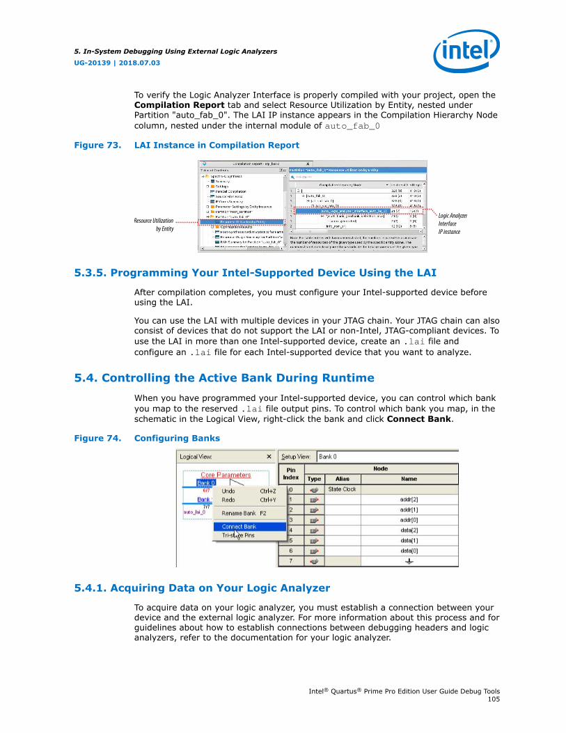
To verify the Logic Analyzer Interface is properly compiled with your project, open theCompilation Report tab and select Resource Utilization by Entity, nested underPartition "auto_fab_0". The LAI IP instance appears in the Compilation Hierarchy Nodecolumn, nested under the internal module of auto_fab_0
Figure 73. LAI Instance in Compilation Report
Logic AnalyzerInterfaceIP instance
Resource Utilization by Entity
5.3.5. Programming Your Intel-Supported Device Using the LAI
After compilation completes, you must configure your Intel-supported device beforeusing the LAI.
You can use the LAI with multiple devices in your JTAG chain. Your JTAG chain can alsoconsist of devices that do not support the LAI or non-Intel, JTAG-compliant devices. Touse the LAI in more than one Intel-supported device, create an .lai file andconfigure an .lai file for each Intel-supported device that you want to analyze.
5.4. Controlling the Active Bank During Runtime
When you have programmed your Intel-supported device, you can control which bankyou map to the reserved .lai file output pins. To control which bank you map, in theschematic in the Logical View, right-click the bank and click Connect Bank.
Figure 74. Configuring Banks
5.4.1. Acquiring Data on Your Logic Analyzer
To acquire data on your logic analyzer, you must establish a connection between yourdevice and the external logic analyzer. For more information about this process and forguidelines about how to establish connections between debugging headers and logicanalyzers, refer to the documentation for your logic analyzer.
5. In-System Debugging Using External Logic Analyzers
UG-20139 | 2018.07.03
Intel® Quartus® Prime Pro Edition User Guide Debug Tools105
5.5. LAI Core Parameters
The table lists the LAI file core parameters:
Table 19. LAI File Core Parameters
Parameter Range Value Description
Pin Count 1 - 255 Number of pins dedicated to the LAI. You must connect the pins to adebug header on the board.Within the device, The Compiler maps each pin to a user-configurable number of internal signals.
Bank Count 1 - 255 Number of internal signals that you want to map to each pin.For example, a Bank Count of 8 implies that you connect eightinternal signals to each pin.
Output/Capture Mode Specifies the acquisition mode. The two options are:• Combinational/Timing—This acquisition mode uses the
external logic analyzer’s internal clock to determine when tosample data.This acquisition mode requires you to manually determine thesample frequency to debug and verify the system, because thedata sampling is asynchronous to the Intel-supported device.This mode is effective if you want to measure timing informationsuch as channel-to-channel skew. For more information about thesampling frequency and the speeds at which it can run, refer tothe external logic analyzer's data sheet.
• Registered/State—This acquisition mode determines when tosample from a signal on the system under test. Consequently, thedata samples are synchronous with the Intel-supported device.The Registered/State mode provides a functional view of theIntel-supported device while it is running. This mode is effectivewhen you verify the functionality of the design.
Clock Specifies the sample clock. You can use any signal in the design as asample clock. However, for best results, use a clock with anoperating frequency fast enough to sample the data that you want toacquire.Note: The Clock parameter is available only when Output/
Capture Mode is set to Registered State.
Power-Up State Specifies the power-up state of the pins designated for use with theLAI. You can select tri-stated for all pins, or selecting a particularbank that you enable.
Related Information
Defining Parameters for the Logic Analyzer Interface on page 103
5.6. In-System Debugging Using External Logic Analyzers RevisionHistory
Document Version Intel QuartusPrime Version
Changes
2018.05.07 18.0.0 • Moved list of LAI File Core Parameters from Configuring the File CoreParameters to its own topic, and added links.
2017.05.08 17.0.0 • Updated Compiling Your Intel Quartus Prime Project• Updated figure: LAI Instance in Compilation Report.
2016.10.31 16.1.0 • Implemented Intel rebranding.
continued...
5. In-System Debugging Using External Logic Analyzers
UG-20139 | 2018.07.03
Intel® Quartus® Prime Pro Edition User Guide Debug Tools106
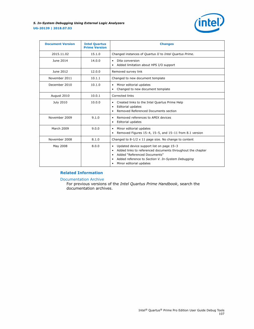
Document Version Intel QuartusPrime Version
Changes
2015.11.02 15.1.0 Changed instances of Quartus II to Intel Quartus Prime.
June 2014 14.0.0 • Dita conversion• Added limitation about HPS I/O support
June 2012 12.0.0 Removed survey link
November 2011 10.1.1 Changed to new document template
December 2010 10.1.0 • Minor editorial updates• Changed to new document template
August 2010 10.0.1 Corrected links
July 2010 10.0.0 • Created links to the Intel Quartus Prime Help• Editorial updates• Removed Referenced Documents section
November 2009 9.1.0 • Removed references to APEX devices• Editorial updates
March 2009 9.0.0 • Minor editorial updates• Removed Figures 15–4, 15–5, and 15–11 from 8.1 version
November 2008 8.1.0 Changed to 8-1/2 x 11 page size. No change to content
May 2008 8.0.0 • Updated device support list on page 15–3• Added links to referenced documents throughout the chapter• Added “Referenced Documents”• Added reference to Section V. In-System Debugging• Minor editorial updates
Related Information
Documentation ArchiveFor previous versions of the Intel Quartus Prime Handbook, search thedocumentation archives.
5. In-System Debugging Using External Logic Analyzers
UG-20139 | 2018.07.03
Intel® Quartus® Prime Pro Edition User Guide Debug Tools107

6. In-System Modification of Memory and ConstantsThe Intel Quartus Prime In-System Memory Content Editor (ISMCE) allows to view andupdate memories and constants at runtime through the JTAG interface. By testingchanges to memory contents in the FPGA while the design is running, you can identify,test, and resolve issues.
The ability to read data from memories and constants can help you identify the sourceof problems, and the write capability allows you to bypass functional issues by writingexpected data.
When you use the In-System Memory Content Editor in conjunction with the SignalTap Logic Analyzer, you can view and debug your design in the hardware lab.
Related Information
• System Debugging Tools Overview on page 7
• Design Debugging with the Signal Tap Logic Analyzer on page 22
6.1. IP Cores Supporting ISMCE
In Intel Arria 10 and Intel Stratix 10 device families, you can use the ISMCE in RAM: 1PORT and the ROM: 1 PORT IP Cores.
Note: To use the ISMCE tool with designs migrated from older devices to Intel Stratix 10devices, replace instances of the altsyncram Intel FPGA IP with the altera_syncramIntel FPGA IP.
Related Information
• Intel Stratix 10 Embedded Memory IP Core ReferencesIn Intel Stratix 10 Embedded Memory User Guide
• About Embedded Memory IP CoresIn Embedded Memory (RAM: 1-PORT, RAM: 2-PORT, ROM: 1-PORT, and ROM:2-PORT) User Guide
• Intel FPGA IP Cores/LPMIn Intel Quartus Prime Help
6.2. Debug Flow with the In-System Memory Content Editor
To debug a design with the In-System Memory Content Editor:
1. Identify the memories and constants that you want to access at runtime.
2. Specify in the design the memory or constant that must be run-time modifiable.
3. Perform a full compilation.
UG-20139 | 2018.07.03
Intel Corporation. All rights reserved. Intel, the Intel logo, Altera, Arria, Cyclone, Enpirion, MAX, Nios, Quartusand Stratix words and logos are trademarks of Intel Corporation or its subsidiaries in the U.S. and/or othercountries. Intel warrants performance of its FPGA and semiconductor products to current specifications inaccordance with Intel's standard warranty, but reserves the right to make changes to any products and servicesat any time without notice. Intel assumes no responsibility or liability arising out of the application or use of anyinformation, product, or service described herein except as expressly agreed to in writing by Intel. Intelcustomers are advised to obtain the latest version of device specifications before relying on any publishedinformation and before placing orders for products or services.*Other names and brands may be claimed as the property of others.
ISO9001:2008Registered
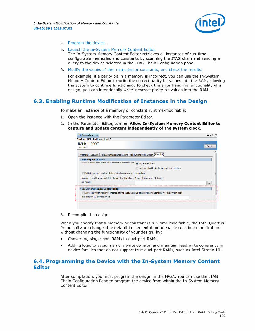
4. Program the device.
5. Launch the In-System Memory Content Editor.The In-System Memory Content Editor retrieves all instances of run-timeconfigurable memories and constants by scanning the JTAG chain and sending aquery to the device selected in the JTAG Chain Configuration pane.
6. Modify the values of the memories or constants, and check the results.
For example, if a parity bit in a memory is incorrect, you can use the In-SystemMemory Content Editor to write the correct parity bit values into the RAM, allowingthe system to continue functioning. To check the error handling functionality of adesign, you can intentionally write incorrect parity bit values into the RAM.
6.3. Enabling Runtime Modification of Instances in the Design
To make an instance of a memory or constant runtime-modifiable:
1. Open the instance with the Parameter Editor.
2. In the Parameter Editor, turn on Allow In-System Memory Content Editor tocapture and update content independently of the system clock.
3. Recompile the design.
When you specify that a memory or constant is run-time modifiable, the Intel QuartusPrime software changes the default implementation to enable run-time modificationwithout changing the functionality of your design, by:
• Converting single-port RAMs to dual-port RAMs
• Adding logic to avoid memory write collision and maintain read write coherency indevice families that do not support true dual-port RAMs, such as Intel Stratix 10.
6.4. Programming the Device with the In-System Memory ContentEditor
After compilation, you must program the design in the FPGA. You can use the JTAGChain Configuration Pane to program the device from within the In-System MemoryContent Editor.
6. In-System Modification of Memory and Constants
UG-20139 | 2018.07.03
Intel® Quartus® Prime Pro Edition User Guide Debug Tools109
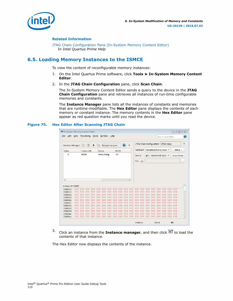
Related Information
JTAG Chain Configuration Pane (In-System Memory Content Editor)In Intel Quartus Prime Help
6.5. Loading Memory Instances to the ISMCE
To view the content of reconfigurable memory instances:
1. On the Intel Quartus Prime software, click Tools ➤ In-System Memory ContentEditor.
2. In the JTAG Chain Configuration pane, click Scan Chain.
The In-System Memory Content Editor sends a query to the device in the JTAGChain Configuration pane and retrieves all instances of run-time configurablememories and constants.
The Instance Manager pane lists all the instances of constants and memoriesthat are runtime-modifiable. The Hex Editor pane displays the contents of eachmemory or constant instance. The memory contents in the Hex Editor paneappear as red question marks until you read the device.
Figure 75. Hex Editor After Scanning JTAG Chain
3. Click an instance from the Instance manager, and then click to load thecontents of that instance.
The Hex Editor now displays the contents of the instance.
6. In-System Modification of Memory and Constants
UG-20139 | 2018.07.03
Intel® Quartus® Prime Pro Edition User Guide Debug Tools110
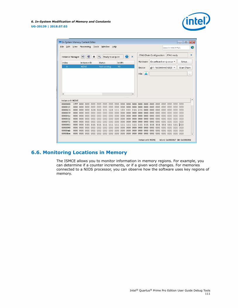
6.6. Monitoring Locations in Memory
The ISMCE allows you to monitor information in memory regions. For example, youcan determine if a counter increments, or if a given word changes. For memoriesconnected to a NIOS processor, you can observe how the software uses key regions ofmemory.
6. In-System Modification of Memory and Constants
UG-20139 | 2018.07.03
Intel® Quartus® Prime Pro Edition User Guide Debug Tools111
• Click to synchronize the Hex Editor to the current instance's content.The Hex Editor displays in red content that changed with respect to the last devicesynchronization.
Figure 76. Hex Editor after Manually Editing Content
• If you want a live output of the memory contents instead of manually
synchronizing, click .
Continuous read is analogous to using Signal Tap in continuous acquisition, withthe memory values appearing as words in the Hex Editor instead of togglingwaveforms.
Note: (Intel Stratix 10 only) ISMCE logic can perform Read/Write operations only when thedesign logic is idle. If the design logic attempts a write or an address changeoperation, the design logic prevails, and the ISMCE operation times out. An errormessage lets you know that the memory connected to the In-System Memory ContentEditor instance is in use, and memory content is not updated.
Related Information
• View, Analyze, and Use Captured Data on page 76
• Read Information from In-System Memory Commands (Processing Menu)In Intel Quartus Prime Help
• Stop In-System Memory Analysis Command (Processing Menu)In Intel Quartus Prime Help
6. In-System Modification of Memory and Constants
UG-20139 | 2018.07.03
Intel® Quartus® Prime Pro Edition User Guide Debug Tools112
6.7. Editing Memory Contents with the Hex Editor Pane
You can edit the contents of instances by typing values directly into the Hex Editorpane.
Black content on the Hex Editor pane means that the value read is the same as lastsynchronization.
1. Type content on the pane.The Hex Editor displays in blue changed content that has not been synchronizedto the device.
Figure 77. Hex Editor after Manually Editing Content
2. Click to synchronize the content to the device.
Note: (Intel Stratix 10 only) ISMCE logic can perform Read/Write operations only when thedesign logic is idle. If the design logic attempts a write or an address changeoperation, the design logic prevails, and the ISMCE operation times out. An errormessage lets you know that the memory connected to the In-System Memory ContentEditor instance is in use, and reports the number of successful writes before thedesign logic requested access to the memory.
Related Information
• Custom Fill Dialog BoxIn Intel Quartus Prime Help
• Write Information to In-System Memory Commands (Processing Menu)In Intel Quartus Prime Help
• Go To Dialog BoxIn Intel Quartus Prime Help
6. In-System Modification of Memory and Constants
UG-20139 | 2018.07.03
Intel® Quartus® Prime Pro Edition User Guide Debug Tools113
• Select Range Dialog BoxIn Intel Quartus Prime Help
6.8. Importing and Exporting Memory Files
The In-System Memory Content Editor allows you to import and export data values formemories that are runtime modifiable. Importing from a data file enables you toquickly load an entire memory image. Exporting to a data file allows you to save thecontents of the memory for future use.
You can import or export files in hex or mif formats.
1. To import a file, click Edit ➤ Import Data from File..., and then select the file toimport.
If the file is not compatible, unexpected data appears in the Hex Editor.
2. To export memory contents to a file, click Edit ➤ Export Data to File..., and thenspecify the name.
Related Information
• Import DataIn Intel Quartus Prime Help
• Export DataIn Intel Quartus Prime Help
• Hexadecimal (Intel-Format) File (.hex) DefinitionIn Intel Quartus Prime Help
• Memory Initialization File (.mif) DefinitionIn Intel Quartus Prime Help
6.9. Access Two or More Devices
If you have more than one device with in-system configurable memories or constantsin a JTAG chain, you can launch multiple In-System Memory Content Editors within theIntel Quartus Prime software to access the memories and constants in each of thedevices. Each window of the In-System Memory Content Editor can access thememories and constants of a single device.
6.10. Scripting Support
The Intel Quartus Prime software allows you to perform runtime modification ofmemories and constants in scripted flows.
You can enable memory and constant instances to be runtime modifiable from the HDLcode. Additionally, the In-System Memory Content Editor supports reading and writingof memory contents via Tcl commands from the insystem_memory_edit package.
Related Information
• Tcl ScriptingIn Scripting User Guide: Intel Quartus Prime Pro Edition
• Command Line ScriptingIn Scripting User Guide: Intel Quartus Prime Pro Edition
6. In-System Modification of Memory and Constants
UG-20139 | 2018.07.03
Intel® Quartus® Prime Pro Edition User Guide Debug Tools114
6.10.1. The insystem_memory_edit Tcl Package
The ::quartus::insystem_memory_edit Tcl package contains the set of Tcl functionsfor reading and editing the contents of memory in an Intel FPGA device using the In-System Memory Content Editor. The quartus_stp and quartus_stp_tcl commandline executables load this package by default.
For the most up-to-date information about the ::quartus::insystem_memory_edit,refer to the Intel Quartus Prime Help.
Related Information
::quartus::insystem_memory_editIn Intel Quartus Prime Help
6.10.1.1. Getting Information about the insystem_memory_edit Package
You can also get information on the insystem_memory_edit package directly fromthe command line:
• For general information about the package, type:
quartus_stp --tcl_eval help -pkg insystem_memory_edit
• For information about a command in the package, type:
quartus_stp --tcl_eval help -cmd <command_name>
6.11. In-System Modification of Memory and Constants RevisionHistory
Document Version Intel QuartusPrime Version
Changes
2018.05.07 18.0.0 • Added support for the Intel Stratix 10 device family.• Removed obsolete example.
2016.10.31 16.1.0 • Implemented Intel rebranding.
2015.11.02 15.1.0 Changed instances of Quartus II to Intel Quartus Prime.
June 2014 14.0.0 • Dita conversion.• Removed references to megafunction and replaced with IP core.
June 2012 12.0.0 Removed survey link.
November 2011 10.0.3 Template update.
December 2010 10.0.2 Changed to new document template. No change to content.
August 2010 10.0.1 Corrected links
July 2010 10.0.0 • Inserted links to Intel Quartus Prime Help• Removed Reference Documents section
November 2009 9.1.0 • Delete references to APEX devices• Style changes
continued...
6. In-System Modification of Memory and Constants
UG-20139 | 2018.07.03
Intel® Quartus® Prime Pro Edition User Guide Debug Tools115

Document Version Intel QuartusPrime Version
Changes
March 2009 9.0.0 No change to content
November 2008 8.1.0 Changed to 8-1/2 x 11 page size. No change to content.
May 2008 8.0.0 • Added reference to Section V. In-System Debugging in volume 3 of theIntel Quartus Prime Handbook on page 16-1
• Removed references to the Mercury device, as it is now considered tobe a “Mature” device
• Added links to referenced documents throughout document• Minor editorial updates
Related Information
Documentation ArchiveFor previous versions of the Intel Quartus Prime Handbook, search thedocumentation archives.
6. In-System Modification of Memory and Constants
UG-20139 | 2018.07.03
Intel® Quartus® Prime Pro Edition User Guide Debug Tools116

7. Design Debugging Using In-System Sources and ProbesThe Signal Tap Logic Analyzer and Signal Probe allow you to read or “tap” internallogic signals during run time as a way to debug your logic design.
Traditional debugging techniques often involve using an external pattern generator toexercise the logic and a logic analyzer to study the output waveforms during run time.
You can make the debugging cycle more efficient when you can drive any internalsignal manually within your design, which allows you to perform the following actions:
• Force the occurrence of trigger conditions set up in the Signal Tap Logic Analyzer
• Create simple test vectors to exercise your design without using external testequipment
• Dynamically control run time control signals with the JTAG chain
The In-System Sources and Probes Editor in the Intel Quartus Prime software extendsthe portfolio of verification tools, and allows you to easily control any internal signaland provides you with a completely dynamic debugging environment. Coupled witheither the Signal Tap Logic Analyzer or Signal Probe, the In-System Sources andProbes Editor gives you a powerful debugging environment in which to generatestimuli and solicit responses from your logic design.
The Virtual JTAG IP core and the In-System Memory Content Editor also give you thecapability to drive virtual inputs into your design. The Intel Quartus Prime softwareoffers a variety of on-chip debugging tools.
The In-System Sources and Probes Editor consists of the ALTSOURCE_PROBE IP coreand an interface to control the ALTSOURCE_PROBE IP core instances during run time.Each ALTSOURCE_PROBE IP core instance provides you with source output ports andprobe input ports, where source ports drive selected signals and probe ports sampleselected signals. When you compile your design, the ALTSOURCE_PROBE IP core setsup a register chain to either drive or sample the selected nodes in your logic design.During run time, the In-System Sources and Probes Editor uses a JTAG connection toshift data to and from the ALTSOURCE_PROBE IP core instances. The figure shows ablock diagram of the components that make up the In-System Sources and ProbesEditor.
UG-20139 | 2018.07.03
Intel Corporation. All rights reserved. Intel, the Intel logo, Altera, Arria, Cyclone, Enpirion, MAX, Nios, Quartusand Stratix words and logos are trademarks of Intel Corporation or its subsidiaries in the U.S. and/or othercountries. Intel warrants performance of its FPGA and semiconductor products to current specifications inaccordance with Intel's standard warranty, but reserves the right to make changes to any products and servicesat any time without notice. Intel assumes no responsibility or liability arising out of the application or use of anyinformation, product, or service described herein except as expressly agreed to in writing by Intel. Intelcustomers are advised to obtain the latest version of device specifications before relying on any publishedinformation and before placing orders for products or services.*Other names and brands may be claimed as the property of others.
ISO9001:2008Registered

Figure 78. In-System Sources and Probes Editor Block Diagram
Design Logic
altsource_probeMegafunction
Probes Sources
JTAGController
FPGAProgramming
Hardware
Quartus PrimeSoftware
FPGA
D Q
D Q
The ALTSOURCE_PROBE IP core hides the detailed transactions between the JTAGcontroller and the registers instrumented in your design to give you a basic buildingblock for stimulating and probing your design. Additionally, the In-System Sources andProbes Editor provides single-cycle samples and single-cycle writes to selected logicnodes. You can use this feature to input simple virtual stimuli and to capture thecurrent value on instrumented nodes. Because the In-System Sources and ProbesEditor gives you access to logic nodes in your design, you can toggle the inputs of low-level components during the debugging process. If used in conjunction with the SignalTap Logic Analyzer, you can force trigger conditions to help isolate your problem andshorten your debugging process.
The In-System Sources and Probes Editor allows you to easily implement controlsignals in your design as virtual stimuli. This feature can be especially helpful forprototyping your design, such as in the following operations:
• Creating virtual push buttons
• Creating a virtual front panel to interface with your design
• Emulating external sensor data
• Monitoring and changing run time constants on the fly
The In-System Sources and Probes Editor supports Tcl commands that interface withall your ALTSOURCE_PROBE IP core instances to increase the level of automation.
7. Design Debugging Using In-System Sources and Probes
UG-20139 | 2018.07.03
Intel® Quartus® Prime Pro Edition User Guide Debug Tools118
Related Information
System Debugging ToolsFor an overview and comparison of all the tools available in the Intel Quartus Primesoftware on-chip debugging tool suite
7.1. Hardware and Software Requirements
The following components are required to use the In-System Sources and ProbesEditor:
• Intel Quartus Prime software
or
• Intel Quartus Prime Lite Edition
• Download Cable (USB-BlasterTM download cable or ByteBlasterTM cable)
• Intel FPGA development kit or user design board with a JTAG connection to deviceunder test
The In-System Sources and Probes Editor supports the following device families:
• Arria® series
• Stratix® series
• Cyclone® series
• MAX® series
7.2. Design Flow Using the In-System Sources and Probes Editor
The In-System Sources and Probes Editor supports an RTL flow. Signals that you wantto view in the In-System Sources and Probes editor are connected to an instance ofthe In-System Sources and Probes IP core.
After you compile the design, you can control each instance via the In-SystemSources and Probes Editor pane or via a Tcl interface.
7. Design Debugging Using In-System Sources and Probes
UG-20139 | 2018.07.03
Intel® Quartus® Prime Pro Edition User Guide Debug Tools119
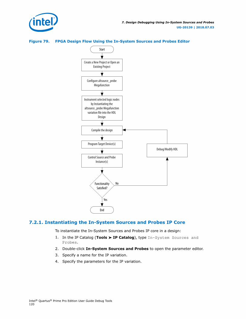
Figure 79. FPGA Design Flow Using the In-System Sources and Probes Editor
Yes
No
Start
End
FunctionalitySatisfied?
Create a New Project or Open an Existing Project
Configure altsource_probe Megafunction
Instrument selected logic nodes by Instantiating the
altsource_probe Megafunction variation file into the HDL
Design
Compile the design
Program Target Device(s)
Control Source and Probe Instance(s)
Debug/Modify HDL
7.2.1. Instantiating the In-System Sources and Probes IP Core
To instantiate the In-System Sources and Probes IP core in a design:
1. In the IP Catalog (Tools ➤ IP Catalog), type In-System Sources andProbes.
2. Double-click In-System Sources and Probes to open the parameter editor.
3. Specify a name for the IP variation.
4. Specify the parameters for the IP variation.
7. Design Debugging Using In-System Sources and Probes
UG-20139 | 2018.07.03
Intel® Quartus® Prime Pro Edition User Guide Debug Tools120

The IP core supports up to 512 bits for each source, and design can include up to128 instances of this IP core.
5. Click Generate or Finish to generate IP core synthesis and simulation filesmatching your specifications.
6. Using the generated template, instantiate the In-System Sources and Probes IPcore in your design.
Note: The In-System Sources and Probes Editor does not support simulation. Remove theIn-System Sources and Probes IP core before you create a simulation netlist.
7.2.2. In-System Sources and Probes IP Core Parameters
Use the template to instantiate the variation file in your design.
Table 20. In-System Sources and Probes IP Port Information
Port Name Required? Direction Comments
probe[] No Input The outputs from your design.
source_clk No Input Source Data is written synchronously to this clock. This input is requiredif you turn on Source Clock in the Advanced Options box in theparameter editor.
source_ena No Input Clock enable signal for source_clk. This input is required if specified inthe Advanced Options box in the parameter editor.
source[] No Output Used to drive inputs to user design.
You can include up to 128 instances of the in-system sources and probes IP core inyour design, if your device has available resources. Each instance of the IP core uses apair of registers per signal for the width of the widest port in the IP core. Additionally,there is some fixed overhead logic to accommodate communication between the IPcore instances and the JTAG controller. You can also specify an additional pair ofregisters per source port for synchronization.
7.3. Compiling the Design
When you compile your design that includes the In-System Sources and ProbesIPcore, the In-System Sources and Probes and SLD Hub Controller IP core are added toyour compilation hierarchy automatically. These IP cores provide communicationbetween the JTAG controller and your instrumented logic.
You can modify the number of connections to your design by editing the In-SystemSources and Probes IP core. To open the design instance you want to modify in theparameter editor, double-click the instance in the Project Navigator. You can thenmodify the connections in the HDL source file. You must recompile your design afteryou make changes.
7.4. Running the In-System Sources and Probes Editor
The In-System Sources and Probes Editor gives you control over allALTSOURCE_PROBE IP core instances within your design. The editor allows you toview all available run time controllable instances of the ALTSOURCE_PROBE IP core inyour design, provides a push-button interface to drive all your source nodes, andprovides a logging feature to store your probe and source data.
7. Design Debugging Using In-System Sources and Probes
UG-20139 | 2018.07.03
Intel® Quartus® Prime Pro Edition User Guide Debug Tools121

To run the In-System Sources and Probes Editor:
• On the Tools menu, click In-System Sources and Probes Editor.
7.4.1. In-System Sources and Probes Editor GUI
The In-System Sources and Probes Editor contains three panes:
• JTAG Chain Configuration—Allows you to specify programming hardware,device, and file settings that the In-System Sources and Probes Editor uses toprogram and acquire data from a device.
• Instance Manager—Displays information about the instances generated whenyou compile a design, and allows you to control data that the In-System Sourcesand Probes Editor acquires.
• In-System Sources and Probes Editor—Logs all data read from the selectedinstance and allows you to modify source data that is written to your device.
When you use the In-System Sources and Probes Editor, you do not need to open aIntel Quartus Prime software project. The In-System Sources and Probes Editorretrieves all instances of the ALTSOURCE_PROBE IP core by scanning the JTAG chainand sending a query to the device selected in the JTAG Chain Configuration pane.You can also use a previously saved configuration to run the In-System Sources andProbes Editor.
Each In-System Sources and Probes Editor pane can access theALTSOURCE_PROBE IP core instances in a single device. If you have more than onedevice containing IP core instances in a JTAG chain, you can launch multiple In-System Sources and Probes Editor panes to access the IP core instances in eachdevice.
7.4.2. Programming Your Device With JTAG Chain Configuration
After you compile your project, you must configure your FPGA before you use the In-System Sources and Probes Editor.
To configure a device to use with the In-System Sources and Probes Editor, performthe following steps:
1. Open the In-System Sources and Probes Editor.
2. In the JTAG Chain Configuration pane, point to Hardware, and then select thehardware communications device. You may be prompted to configure yourhardware; in this case, click Setup.
3. From the Device list, select the FPGA device to which you want to download thedesign (the device may be automatically detected). You may need to click ScanChain to detect your target device.
4. In the JTAG Chain Configuration pane, click to browse for the SRAM Object File(.sof) that includes the In-System Sources and Probes instance or instances.(The .sof may be automatically detected).
5. Click Program Device to program the target device.
7.4.3. Instance Manager
The Instance Manager pane provides a list of all ALTSOURCE_PROBE instances inthe design, and allows you to configure data acquisition.
7. Design Debugging Using In-System Sources and Probes
UG-20139 | 2018.07.03
Intel® Quartus® Prime Pro Edition User Guide Debug Tools122

The Instance Manager pane contains the following buttons and sub-panes:
• Read Probe Data—Samples the probe data in the selected instance and displaysthe probe data in the In-System Sources and Probes Editor pane.
• Continuously Read Probe Data—Continuously samples the probe data of theselected instance and displays the probe data in the In-System Sources andProbes Editor pane; you can modify the sample rate via the Probe readinterval setting.
• Stop Continuously Reading Probe Data—Cancels continuous sampling of theprobe of the selected instance.
• Read Source Data—Reads the data of the sources in the selected instances.
• Probe Read Interval—Displays the sample interval of all the In-System Sourcesand Probe instances in your design; you can modify the sample interval by clickingManual.
• Event Log—Controls the event log that appears in the In-System Sources andProbes Editor pane.
• Write Source Data—Allows you to manually or continuously write data to thesystem.
Beside each entry, the Instance Manager pane displays the instance status. Thepossible instance statuses are Not running Offloading data, Updating data, andUnexpected JTAG communication error.
7.4.4. In-System Sources and Probes Editor Pane
The In-System Sources and Probes Editor pane allows you to view data from allsources and probes in your design.
The data is organized according to the index number of the instance. The editorprovides an easy way to manage your signals, and allows you to rename signals orgroup them into buses. All data collected from in-system source and probe nodes isrecorded in the event log and you can view the data as a timing diagram.
7.4.4.1. Reading Probe Data
You can read data by selecting the ALTSOURCE_PROBE instance in the InstanceManager pane and clicking Read Probe Data.
This action produces a single sample of the probe data and updates the data columnof the selected index in the In-System Sources and Probes Editor pane. You cansave the data to an event log by turning on the Save data to event log option in theInstance Manager pane.
If you want to sample data from your probe instance continuously, in the InstanceManager pane, click the instance you want to read, and then click Continuouslyread probe data. While reading, the status of the active instance shows Unloading.You can read continuously from multiple instances.
You can access read data with the shortcut menus in the Instance Manager pane.
7. Design Debugging Using In-System Sources and Probes
UG-20139 | 2018.07.03
Intel® Quartus® Prime Pro Edition User Guide Debug Tools123
To adjust the probe read interval, in the Instance Manager pane, turn on theManual option in the Probe read interval sub-pane, and specify the sample rate inthe text field next to the Manual option. The maximum sample rate depends on yourcomputer setup. The actual sample rate is shown in the Current interval box. Youcan adjust the event log window buffer size in the Maximum Size box.
7.4.4.2. Writing Data
To modify the source data you want to write into the ALTSOURCE_PROBE instance,click the name field of the signal you want to change. For buses of signals, you candouble-click the data field and type the value you want to drive out to theALTSOURCE_PROBE instance. The In-System Sources and Probes Editor stores themodified source data values in a temporary buffer.
Modified values that are not written out to the ALTSOURCE_PROBE instances appear inred. To update the ALTSOURCE_PROBE instance, highlight the instance in theInstance Manager pane and click Write source data. The Write source datafunction is also available via the shortcut menus in the Instance Manager pane.
The In-System Sources and Probes Editor provides the option to continuously updateeach ALTSOURCE_PROBE instance. Continuous updating allows any modifications youmake to the source data buffer to also write immediately to the ALTSOURCE_PROBEinstances. To continuously update the ALTSOURCE_PROBE instances, change theWrite source data field from Manually to Continuously.
7.4.4.3. Organizing Data
The In-System Sources and Probes Editor pane allows you to group signals intobuses, and also allows you to modify the display options of the data buffer.
To create a group of signals, select the node names you want to group, right-click andselect Group. You can modify the display format in the Bus Display Format and theBus Bit order shortcut menus.
The In-System Sources and Probes Editor pane allows you to rename any signal.To rename a signal, double-click the name of the signal and type the new name.
The event log contains a record of the most recent samples. The buffer size isadjustable up to 128k samples. The time stamp for each sample is logged and isdisplayed above the event log of the active instance as you move your pointer overthe data samples.
You can save the changes that you make and the recorded data to a Sources andProbes File (.spf). To save changes, on the File menu, click Save. The file containsall the modifications you made to the signal groups, as well as the current data eventlog.
7.5. Tcl interface for the In-System Sources and Probes Editor
To support automation, the In-System Sources and Probes Editor supports theprocedures described in this chapter in the form of Tcl commands. The Tcl package forthe In-System Sources and Probes Editor is included by default when you runquartus_stp.
7. Design Debugging Using In-System Sources and Probes
UG-20139 | 2018.07.03
Intel® Quartus® Prime Pro Edition User Guide Debug Tools124
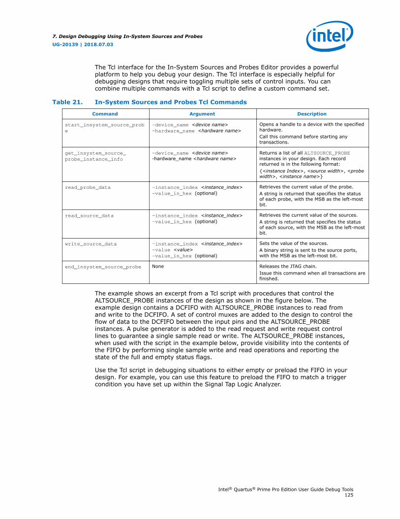
The Tcl interface for the In-System Sources and Probes Editor provides a powerfulplatform to help you debug your design. The Tcl interface is especially helpful fordebugging designs that require toggling multiple sets of control inputs. You cancombine multiple commands with a Tcl script to define a custom command set.
Table 21. In-System Sources and Probes Tcl Commands
Command Argument Description
start_insystem_source_probe
-device_name <device name>-hardware_name <hardware name>
Opens a handle to a device with the specifiedhardware.Call this command before starting anytransactions.
get_insystem_source_probe_instance_info
-device_name <device name>-hardware_name <hardware name>
Returns a list of all ALTSOURCE_PROBEinstances in your design. Each recordreturned is in the following format:{<instance Index>, <source width>, <probewidth>, <instance name>}
read_probe_data -instance_index <instance_index>-value_in_hex (optional)
Retrieves the current value of the probe.A string is returned that specifies the statusof each probe, with the MSB as the left-mostbit.
read_source_data -instance_index <instance_index>-value_in_hex (optional)
Retrieves the current value of the sources.A string is returned that specifies the statusof each source, with the MSB as the left-mostbit.
write_source_data -instance_index <instance_index>-value <value>-value_in_hex (optional)
Sets the value of the sources.A binary string is sent to the source ports,with the MSB as the left-most bit.
end_insystem_source_probe None Releases the JTAG chain.Issue this command when all transactions arefinished.
The example shows an excerpt from a Tcl script with procedures that control theALTSOURCE_PROBE instances of the design as shown in the figure below. Theexample design contains a DCFIFO with ALTSOURCE_PROBE instances to read fromand write to the DCFIFO. A set of control muxes are added to the design to control theflow of data to the DCFIFO between the input pins and the ALTSOURCE_PROBEinstances. A pulse generator is added to the read request and write request controllines to guarantee a single sample read or write. The ALTSOURCE_PROBE instances,when used with the script in the example below, provide visibility into the contents ofthe FIFO by performing single sample write and read operations and reporting thestate of the full and empty status flags.
Use the Tcl script in debugging situations to either empty or preload the FIFO in yourdesign. For example, you can use this feature to preload the FIFO to match a triggercondition you have set up within the Signal Tap Logic Analyzer.
7. Design Debugging Using In-System Sources and Probes
UG-20139 | 2018.07.03
Intel® Quartus® Prime Pro Edition User Guide Debug Tools125
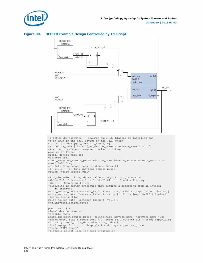
Figure 80. DCFIFO Example Design Controlled by Tcl Script
Write_clock
write_reqdata[7..0]
write_clock
read_req
read_clock
wr_full
Q[7..0]
rd_empty
data_out
read_clocksource_read_sel
s_read_req
s_write_req
rd_req_in
wr_req_in
data_in[7..0]
altsource_probe(Instance 1)
altsource_probe(Instance 0)
source_write_sel
s_data[7..0]D Q
D Q
## Setup USB hardware - assumes only USB Blaster is installed and## an FPGA is the only device in the JTAG chainset usb [lindex [get_hardware_names] 0]set device_name [lindex [get_device_names -hardware_name $usb] 0]## write procedure : argument value is integerproc write {value} {global device_name usbvariable fullstart_insystem_source_probe -device_name $device_name -hardware_name $usb#read full flagset full [read_probe_data -instance_index 0]if {$full == 1} {end_insystem_source_probereturn "Write Buffer Full"}##toggle select line, drive value onto port, toggle enable##bits 7:0 of instance 0 is S_data[7:0]; bit 8 = S_write_req;##bit 9 = Source_write_sel##int2bits is custom procedure that returns a bitstring from an integer ## argumentwrite_source_data -instance_index 0 -value /[int2bits [expr 0x200 | $value]]write_source_data -instance_index 0 -value [int2bits [expr 0x300 | $value]]##clear transactionwrite_source_data -instance_index 0 -value 0end_insystem_source_probe}proc read {} {global device_name usbvariable emptystart_insystem_source_probe -device_name $device_name -hardware_name $usb##read empty flag : probe port[7:0] reads FIFO output; bit 8 reads empty_flagset empty [read_probe_data -instance_index 1]if {[regexp {1........} $empty]} { end_insystem_source_probereturn "FIFO empty" }## toggle select line for read transaction
7. Design Debugging Using In-System Sources and Probes
UG-20139 | 2018.07.03
Intel® Quartus® Prime Pro Edition User Guide Debug Tools126
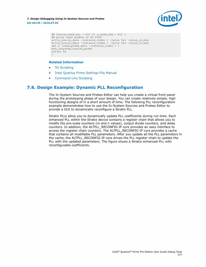
## Source_read_sel = bit 0; s_read_reg = bit 1## pulse read enable on DC FIFOwrite_source_data -instance_index 1 -value 0x1 -value_in_hexwrite_source_data -instance_index 1 -value 0x3 -value_in_hexset x [read_probe_data -instance_index 1 ]end_insystem_source_probereturn $x}
Related Information
• Tcl Scripting
• Intel Quartus Prime Settings File Manual
• Command Line Scripting
7.6. Design Example: Dynamic PLL Reconfiguration
The In-System Sources and Probes Editor can help you create a virtual front panelduring the prototyping phase of your design. You can create relatively simple, highfunctioning designs of in a short amount of time. The following PLL reconfigurationexample demonstrates how to use the In-System Sources and Probes Editor toprovide a GUI to dynamically reconfigure a Stratix PLL.
Stratix PLLs allow you to dynamically update PLL coefficients during run time. Eachenhanced PLL within the Stratix device contains a register chain that allows you tomodify the pre-scale counters (m and n values), output divide counters, and delaycounters. In addition, the ALTPLL_RECONFIG IP core provides an easy interface toaccess the register chain counters. The ALTPLL_RECONFIG IP core provides a cachethat contains all modifiable PLL parameters. After you update all the PLL parameters inthe cache, the ALTPLL_RECONFIG IP core drives the PLL register chain to update thePLL with the updated parameters. The figure shows a Stratix-enhanced PLL withreconfigurable coefficients.
7. Design Debugging Using In-System Sources and Probes
UG-20139 | 2018.07.03
Intel® Quartus® Prime Pro Edition User Guide Debug Tools127
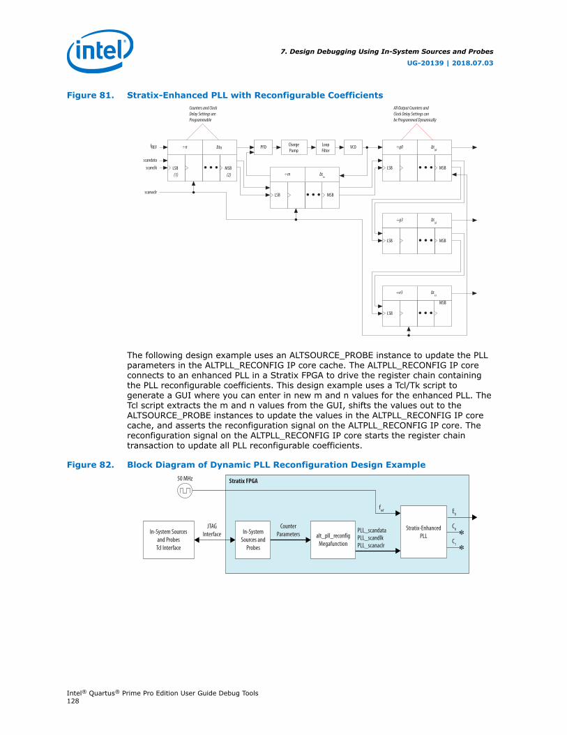
Figure 81. Stratix-Enhanced PLL with Reconfigurable Coefficients
÷n Δtn
Δtm
÷m
÷g0 Δtg0
÷e3 Δte3
÷g3 Δtg3
PFD VCOChargePump
LoopFilter
fREF
scandata
scanclk
scanaclr
Counters and ClockDelay Settings areProgrammable
All Output Counters andClock Delay Settings canbe Programmed Dynamically
LSB MSB
LSB MSB
LSB MSB
LSB MSB
LSB
MSB
(1) (2)
The following design example uses an ALTSOURCE_PROBE instance to update the PLLparameters in the ALTPLL_RECONFIG IP core cache. The ALTPLL_RECONFIG IP coreconnects to an enhanced PLL in a Stratix FPGA to drive the register chain containingthe PLL reconfigurable coefficients. This design example uses a Tcl/Tk script togenerate a GUI where you can enter in new m and n values for the enhanced PLL. TheTcl script extracts the m and n values from the GUI, shifts the values out to theALTSOURCE_PROBE instances to update the values in the ALTPLL_RECONFIG IP corecache, and asserts the reconfiguration signal on the ALTPLL_RECONFIG IP core. Thereconfiguration signal on the ALTPLL_RECONFIG IP core starts the register chaintransaction to update all PLL reconfigurable coefficients.
Figure 82. Block Diagram of Dynamic PLL Reconfiguration Design Example
In-System Sourcesand ProbesTcl Interface
JTAGInterface
CounterParameters
Stratix FPGA50 MHz
PLL_scandataPLL_scandlkPLL_scanaclr
E0
C0
C1
fref
Stratix-EnhancedPLLalt_pll_reconfig
Megafunction
In-SystemSources and
Probes
7. Design Debugging Using In-System Sources and Probes
UG-20139 | 2018.07.03
Intel® Quartus® Prime Pro Edition User Guide Debug Tools128
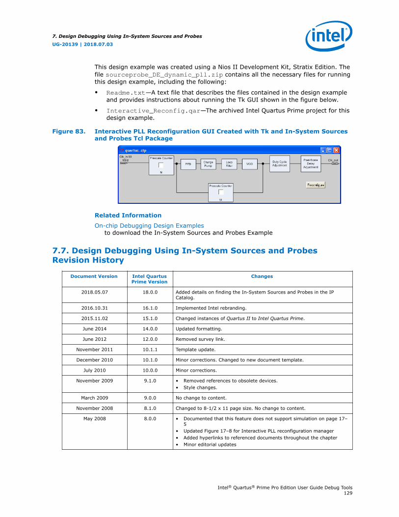
This design example was created using a Nios II Development Kit, Stratix Edition. Thefile sourceprobe_DE_dynamic_pll.zip contains all the necessary files for runningthis design example, including the following:
• Readme.txt—A text file that describes the files contained in the design exampleand provides instructions about running the Tk GUI shown in the figure below.
• Interactive_Reconfig.qar—The archived Intel Quartus Prime project for thisdesign example.
Figure 83. Interactive PLL Reconfiguration GUI Created with Tk and In-System Sourcesand Probes Tcl Package
Related Information
On-chip Debugging Design Examplesto download the In-System Sources and Probes Example
7.7. Design Debugging Using In-System Sources and ProbesRevision History
Document Version Intel QuartusPrime Version
Changes
2018.05.07 18.0.0 Added details on finding the In-System Sources and Probes in the IPCatalog.
2016.10.31 16.1.0 Implemented Intel rebranding.
2015.11.02 15.1.0 Changed instances of Quartus II to Intel Quartus Prime.
June 2014 14.0.0 Updated formatting.
June 2012 12.0.0 Removed survey link.
November 2011 10.1.1 Template update.
December 2010 10.1.0 Minor corrections. Changed to new document template.
July 2010 10.0.0 Minor corrections.
November 2009 9.1.0 • Removed references to obsolete devices.• Style changes.
March 2009 9.0.0 No change to content.
November 2008 8.1.0 Changed to 8-1/2 x 11 page size. No change to content.
May 2008 8.0.0 • Documented that this feature does not support simulation on page 17–5
• Updated Figure 17–8 for Interactive PLL reconfiguration manager• Added hyperlinks to referenced documents throughout the chapter• Minor editorial updates
7. Design Debugging Using In-System Sources and Probes
UG-20139 | 2018.07.03
Intel® Quartus® Prime Pro Edition User Guide Debug Tools129

Related Information
Documentation ArchiveFor previous versions of the Intel Quartus Prime Handbook, search thedocumentation archives.
7. Design Debugging Using In-System Sources and Probes
UG-20139 | 2018.07.03
Intel® Quartus® Prime Pro Edition User Guide Debug Tools130

8. Analyzing and Debugging Designs with System Console
8.1. Introduction to System Console
System Console provides visibility into your design and allows you to perform system-level debug on a FPGA at run-time. System Console performs tests on debug-enabledPlatform Designer instantiated IP cores. A variety of debug services provide read andwrite access to elements in your design. You can perform the following tasks withSystem Console and the tools built on top of System Console:
• Bring up boards with both finalized and partially complete designs.
• Perform remote debug with internet access.
• Automate run-time verification through scripting across multiple devices in yoursystem.
• Test serial links with point-and-click configuration tuning in the Transceiver Toolkit.
• Debug memory interfaces with the External Memory Interface Toolkit.
• Integrate your debug IP into the debug platform.
• Perform system verification with MATLAB/Simulink.
UG-20139 | 2018.07.03
Intel Corporation. All rights reserved. Intel, the Intel logo, Altera, Arria, Cyclone, Enpirion, MAX, Nios, Quartusand Stratix words and logos are trademarks of Intel Corporation or its subsidiaries in the U.S. and/or othercountries. Intel warrants performance of its FPGA and semiconductor products to current specifications inaccordance with Intel's standard warranty, but reserves the right to make changes to any products and servicesat any time without notice. Intel assumes no responsibility or liability arising out of the application or use of anyinformation, product, or service described herein except as expressly agreed to in writing by Intel. Intelcustomers are advised to obtain the latest version of device specifications before relying on any publishedinformation and before placing orders for products or services.*Other names and brands may be claimed as the property of others.
ISO9001:2008Registered

Figure 84. System Console Tools(Tools) shows the applications that interact with System Console. The System Console API supports servicesthat access your design in operation. Some services have specific hardware requirements.
Tcl ConsoleTransceiver
Debug ToolkitADC Toolkit Bus Analyzer EMIF Toolkit Toolkit API
System Console Tcl(Command-Line Interface)
System Console GUI Interface
System Console
Ethernet Processor Master Bytestream Others
TCP/IP Nios II JTAG Master JTAG UART ISSP
Nios II withJTAG Debug
USB DebugMaster
Tools
API
HardwareRequirements
Note: Use debug links to connect the host to the target you are debugging.
Related Information
• Introduction to Intel Memory SolutionIn External Memory Interface Handbook Volume 1
• Debugging Transceiver Links on page 196
• Application Note 693: Remote Hardware Debugging over TCP/IP for Intel SoC
• Application Note 624: Debugging with System Console over TCP/IP
• White Paper 01208: Hardware in the Loop from the MATLAB/Simulink Environment
• System Console Online Training
8.2. System Console Debugging Flow
To debug a design with the System Console, you must perform a series of steps:
1. Add an IP Core to the Platform Designer system.
2. Generate the Platform Designer system.
3. Compile the design.
4. Connect a board and program the FPGA.
8. Analyzing and Debugging Designs with System Console
UG-20139 | 2018.07.03
Intel® Quartus® Prime Pro Edition User Guide Debug Tools132
5. Start the System Console.
6. Locate and open a System Console service.
7. Perform debug operations with the service.
8. Close the service.
8.3. IP Cores that Interact with System Console
System Console runs on your host computer and communicates with your runningdesign through debug agents. Debug agents are soft-logic embedded in some IP coresthat enable debug communication with the host computer.
You instantiate debug IP cores using the Platform Designer IP Catalog. Some IP coresare enabled for debug by default, while you can enable debug for other IP coresthrough options in the parameter editor. Some debug agents have multiple purposes.
When you use IP cores with embedded debug in your design, you can make largeportions of the design accessible. Debug agents allow you to read and write tomemory and alter peripheral registers from the host computer.
Services associated with debug agents in the running design can open and close asneeded. System Console determines the communication protocol with the debugagent. The communication protocol determines the best board connection to use forcommand and data transmission.
The Programmable SRAM Object File (.sof) provides the System Console withchannel communication information. When System Console opens in the Intel QuartusPrime software or Platform Designer while your design is open, any existing .sof isautomatically found and linked to the detected running device. In a complex system,you may need to link the design and device manually.
Related Information
WP-01170 System-Level Debugging and Monitoring of FPGA Designs
8.3.1. Services Provided through Debug Agents
By adding the appropriate debug agent to your design, System Console services canuse the associated capabilities of the debug agent.
Table 22. Common Services for System Console
Service Function Debug Agent Providing Service
master Access memory-mapped (Avalon-MM or AXI)slaves connected to the master interface.
• Nios II with debug• JTAG to Avalon Master Bridge• USB Debug Master
slave Allows the host to access a single slave withoutneeding to know the location of the slave in thehost's memory map. Any slave that is accessibleto a System Console master can provide thisservice.
• Nios II with debug• JTAG to Avalon Master Bridge• USB Debug Master
continued...
8. Analyzing and Debugging Designs with System Console
UG-20139 | 2018.07.03
Intel® Quartus® Prime Pro Edition User Guide Debug Tools133
Service Function Debug Agent Providing Service
If an SRAM Object File (.sof) is loaded, thenslaves controlled by a debug master provide theslave service.
processor • Start, stop, or step the processor.• Read and write processor registers.
Nios II with debug
JTAG UART The JTAG UART is an Avalon-MM slave device thatyou can use in conjunction with System Consoleto send and receive byte streams.
JTAG UART
Note: The following IP cores in the IP Catalog do not support VHDL simulation generation inthe current version of the Intel Quartus Prime software:
• JTAG Debug Link
• JTAG Hub Controller System
• USB Debug Link
Related Information
• System Console Examples and Tutorials on page 189
• System Console Commands on page 137
8.4. Starting System Console
8.4.1. Starting System Console from Nios II Command Shell
1. On the Windows Start menu, click All Programs ➤ Intel ➤ Nios II EDS<version> ➤ Nios II<version> ➤ Command Shell..
2. Type system-console.
3. Type -- help for System Console help.
4. Type system-console --project_dir=<project directory> to point to adirectory that contains .qsf or .sof files.
8.4.2. Starting Stand-Alone System Console
You can get the stand-alone version of System Console as part of the Intel QuartusPrime software Programmer and Tools installer on the Altera website.
1. Navigate to the Download Center page and click the Additional Software tab.
2. On the Windows Start menu, click All Programs ➤ Intel FPGA <version> ➤Programmer and Tools ➤ System Console.
Related Information
Intel Download Center
8.4.3. Starting System Console from Platform Designer
Click Tools ➤ System Console.
8. Analyzing and Debugging Designs with System Console
UG-20139 | 2018.07.03
Intel® Quartus® Prime Pro Edition User Guide Debug Tools134
8.4.4. Starting System Console from Intel Quartus Prime
Click Tools ➤ System Debugging Tools ➤ System Console.
8.4.5. Customizing Startup
You can customize your System Console environment, as follows:
• Add commands to the system_console_rc configuration file located at:
— <$HOME>/system_console/system_console_rc.tcl
The file in this location is the user configuration file, which only affects the ownerof the home directory.
• Specify your own design startup configuration file with the command-lineargument --rc_script=<path_to_script>, when you launch System Consolefrom the Nios II command shell.
• Use the system_console_rc.tcl file in combination with your customrc_script.tcl file. In this case, the system_console_rc.tcl file performsSystem Console actions, and the rc_script.tcl file performs your debuggingactions.
On startup, System Console automatically runs the Tcl commands in these files. Thecommands in the system_console_rc.tcl file run first, followed by the commandsin the rc_script.tcl file.
8.5. System Console GUI
The System Console GUI consists of a main window with multiple panes, and allowsyou to interact with the design currently running on the host computer.
• System Explorer—Displays the hierarchy of the System Console virtual filesystem in your design, including board connections, devices, designs, and scripts.
• Workspace—Displays available toolkits including the ADC Toolkit, TransceiverToolkit, Toolkits, GDB Server Control Panel, and Bus Analyzer. Click the Toolsmenu to launch applications.
• Tcl Console—A window that allows you to interact with your design using Tclscripts, for example, sourcing scripts, writing procedures, and using SystemConsole API.
• Messages—Displays status, warning, and error messages related to connectionsand debug actions.
8. Analyzing and Debugging Designs with System Console
UG-20139 | 2018.07.03
Intel® Quartus® Prime Pro Edition User Guide Debug Tools135
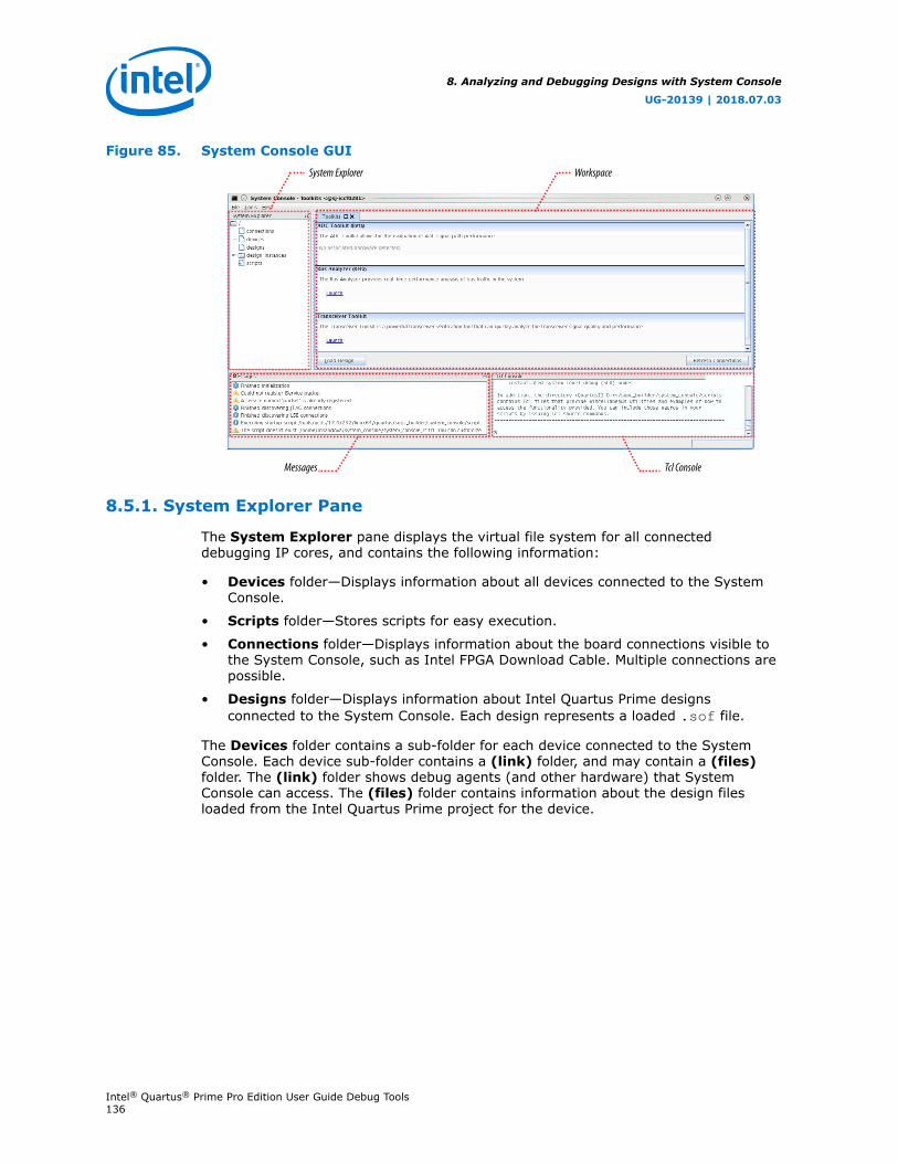
Figure 85. System Console GUISystem Explorer Workspace
Messages Tcl Console
8.5.1. System Explorer Pane
The System Explorer pane displays the virtual file system for all connecteddebugging IP cores, and contains the following information:
• Devices folder—Displays information about all devices connected to the SystemConsole.
• Scripts folder—Stores scripts for easy execution.
• Connections folder—Displays information about the board connections visible tothe System Console, such as Intel FPGA Download Cable. Multiple connections arepossible.
• Designs folder—Displays information about Intel Quartus Prime designsconnected to the System Console. Each design represents a loaded .sof file.
The Devices folder contains a sub-folder for each device connected to the SystemConsole. Each device sub-folder contains a (link) folder, and may contain a (files)folder. The (link) folder shows debug agents (and other hardware) that SystemConsole can access. The (files) folder contains information about the design filesloaded from the Intel Quartus Prime project for the device.
8. Analyzing and Debugging Designs with System Console
UG-20139 | 2018.07.03
Intel® Quartus® Prime Pro Edition User Guide Debug Tools136
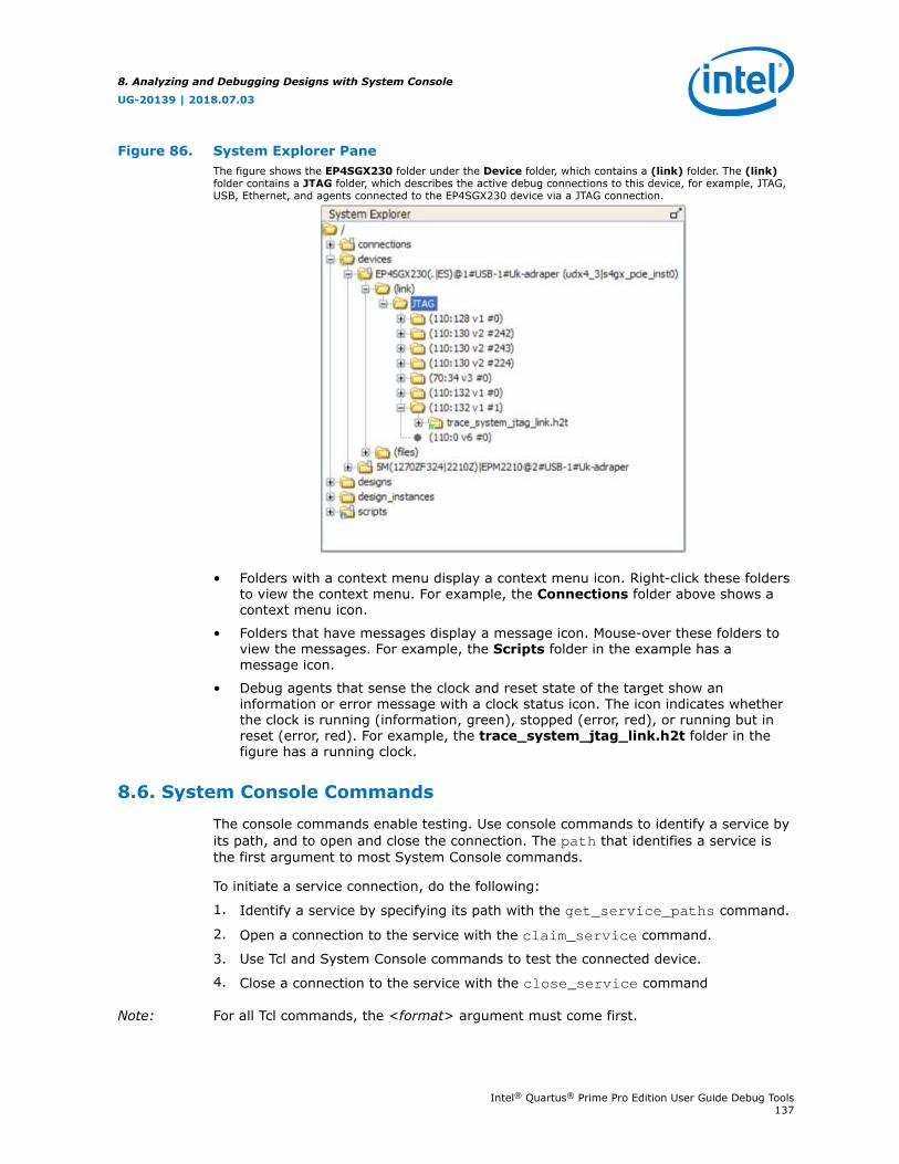
Figure 86. System Explorer PaneThe figure shows the EP4SGX230 folder under the Device folder, which contains a (link) folder. The (link)folder contains a JTAG folder, which describes the active debug connections to this device, for example, JTAG,USB, Ethernet, and agents connected to the EP4SGX230 device via a JTAG connection.
• Folders with a context menu display a context menu icon. Right-click these foldersto view the context menu. For example, the Connections folder above shows acontext menu icon.
• Folders that have messages display a message icon. Mouse-over these folders toview the messages. For example, the Scripts folder in the example has amessage icon.
• Debug agents that sense the clock and reset state of the target show aninformation or error message with a clock status icon. The icon indicates whetherthe clock is running (information, green), stopped (error, red), or running but inreset (error, red). For example, the trace_system_jtag_link.h2t folder in thefigure has a running clock.
8.6. System Console Commands
The console commands enable testing. Use console commands to identify a service byits path, and to open and close the connection. The path that identifies a service isthe first argument to most System Console commands.
To initiate a service connection, do the following:
1. Identify a service by specifying its path with the get_service_paths command.
2. Open a connection to the service with the claim_service command.
3. Use Tcl and System Console commands to test the connected device.
4. Close a connection to the service with the close_service command
Note: For all Tcl commands, the <format> argument must come first.
8. Analyzing and Debugging Designs with System Console
UG-20139 | 2018.07.03
Intel® Quartus® Prime Pro Edition User Guide Debug Tools137

Table 23. System Console Commands
Command Arguments Function
get_service_types N/A Returns a list of service types that SystemConsole manages. Examples of service typesinclude master, bytestream, processor, sld,jtag_debug, device, and design.
get_service_paths • <service-type>• <device>—Returns
services in the samespecified device. Theargument can be a deviceor another service in thedevice.
• <hpath>—Returnsservices whose hpathstarts with the specifiedprefix.
• <type>—Returns serviceswhose debug typematches this value.Particularly useful whenopening slave services.
• <type>—Returns serviceson the same developmentboards as the argument.Specify a board service, orany other service on thesame board.
Allows you to filter the services which arereturned.
claim_service • <service-type>• <service-path>• <claim-group>• <claims>
Provides finer control of the portion of a serviceyou want to use.claim_service returns a new path whichrepresents a use of that service. Each use isindependent. Calling claim_service multipletimes returns different values each time, buteach allows access to the service until closed.
close_service • <service-type>• <service-path>
Closes the specified service type at the specifiedpath.
is_service_open • <service-type>• <service-type>
Returns 1 if the service type provided by thepath is open, 0 if the service type is closed.
get_services_to_add N/A Returns a list of all services that are instantiablewith the add_service command.
add_service • <service-type>• <instance-name>• optional-parameters
Adds a service of the specified service type withthe given instance name. Runget_services_to_add to retrieve a list ofinstantiable services. This command returns thepath where the service was added.Run help add_service <service-type> to getspecific help about that service type, includingany parameters that might be required for thatservice.
add_service gdbserver • <Processor Service>• <port number>
Instantiates a gdbserver.
add_service tcp • <instance name>• <ip_addr>• <port_number>
Allows you to connect to a TCP/IP port thatprovides a debug link over ethernet. See AN693(Remote Hardware Debugging over TCP/IP forIntel FPGA SoC) for more information.
continued...
8. Analyzing and Debugging Designs with System Console
UG-20139 | 2018.07.03
Intel® Quartus® Prime Pro Edition User Guide Debug Tools138

Command Arguments Function
add_servicetransceiver_channel_rx
• <data_pattern_checker>• <path>• <transceiver path>• <transceiver channel
address>• <reconfig path>• <reconfig channel
address>
Instantiates a Transceiver Toolkit receiverchannel.
add_servicetransceiver_channel_tx
• <data_pattern_generator>
• <path>• <transceiver path>• <transceiver channel
address>• <reconfig path>• <reconfig channel
address>
Instantiates a Transceiver Toolkit transmitterchannel.
add_servicetransceiver_debug_link
• <transceiver_channel_txpath>
• <transceiver_channel_rxpath>
Instantiates a Transceiver Toolkit debug link.
get_version N/A Returns the current System Console version andbuild number.
get_claimed_services • <claim> For the given claim group, returns a list ofservices claimed. The returned list consists ofpairs of paths and service types. Each pair is oneclaimed service.
refresh_connections N/A Scans for available hardware and updates theavailable service paths if there have been anychanges.
send_message • <level>• <message>
Sends a message of the given level to themessage window. Available levels are info,warning, error, and debug.
Related Information
Remote Hardware Debugging over TCP/IP for SoC Devices
8.7. Running System Console in Command-Line Mode
You can run System Console in command line mode and either work interactively orrun a Tcl script. System Console prints the output in the console window.
• --cli—Runs System Console in command-line mode.
• --project_dir=<project dir>—Directs System Console to the location ofyour hardware project. Also works in GUI mode.
• --script=<your script>.tcl—Directs System Console to run your Tcl script.
• --help— Lists all available commands. Typing --help <command name>provides the syntax and arguments of the command.
System Console provides command completion if you type the beginning letters of acommand and then press the Tab key.
8. Analyzing and Debugging Designs with System Console
UG-20139 | 2018.07.03
Intel® Quartus® Prime Pro Edition User Guide Debug Tools139
8.8. System Console Services
Intel's System Console services provide access to hardware modules instantiated inyour FPGA. Services vary in the type of debug access they provide.
8.8.1. Locating Available Services
System Console uses a virtual file system to organize the available services, which issimilar to the /dev location on Linux systems. Board connection, device type, andIP names are all part of a service path. Instances of services are referred to by theirunique service path in the file system. To retrieve service paths for a particularservice, use the command get_service_paths <service-type>.
Example 12. Locating a Service Path
#We are interested in master services.set service_type "master"
#Get all the paths as a list.set master_service_paths [get_service_paths $service_type]
#We are interested in the first service in the list.set master_index 0
#The path of the first master.set master_path [lindex $master_service_paths $master_index]
#Or condense the above statements into one statement:set master_path [lindex [get_service_paths master] 0]
System Console commands require service paths to identify the service instance youwant to access. The paths for different components can change between runs ofSystem Console and between versions. Use the get_service_paths command toobtain service paths.
The string values of service paths change with different releases of the tool. Use themarker_node_info command to get information from the path.
System Console automatically discovers most services at startup. System Consoleautomatically scans for all JTAG and USB-based service instances and retrieves theirservice paths. System Console does not automatically discover some services, such asTCP/IP. Use add_service to inform System Console about those services.
Example 13. Marker_node_info
Use the marker_node_info command to get information about the discoveredservices.
set slave_path [get_service_paths -type altera_avalon_uart.slave slave]array set uart_info [marker_node_info $slave_path]echo $uart_info(full_hpath)
8.8.2. Opening and Closing Services
After you have a service path to a particular service instance, you can access theservice for use.
8. Analyzing and Debugging Designs with System Console
UG-20139 | 2018.07.03
Intel® Quartus® Prime Pro Edition User Guide Debug Tools140
The claim_service command directs System Console to start using a particularservice instance, and with no additional arguments, claims a service instance forexclusive use.
Example 14. Opening a Service
set service_type "master"set claim_path [claim_service $service_type $master_path mylib];#Claims service.
You can pass additional arguments to the claim_service command to direct SystemConsole to start accessing a particular portion of a service instance. For example, ifyou use the master service to access memory, then use claim_service to onlyaccess the address space between 0x0 and 0x1000. System Console then allowsother users to access other memory ranges, and denies access to the claimed memoryrange. The claim_service command returns a newly created service path that youcan use to access your claimed resources.
You can access a service after you open it. When you finish accessing a serviceinstance, use the close_service command to direct System Console to make thisresource available to other users.
Example 15. Closing a Service
close_service master $claim_path; #Closes the service.
8.8.3. SLD Service
The SLD Service shifts values into the instruction and data registers of SLD nodes andcaptures the previous value. When interacting with a SLD node, start by acquiringexclusive access to the node on an opened service.
Example 16. SLD Service
set timeout_in_ms 1000set lock_failed [sld_lock $sld_service_path $timeout_in_ms]
This code attempts to lock the selected SLD node. If it is already locked, sld_lockwaits for the specified timeout. Confirm the procedure returns non-zero beforeproceeding. Set the instruction register and capture the previous one:
if {$lock_failed} { return}set instr 7set delay_us 1000set capture [sld_access_ir $sld_service_path $instr $delay_us]
The 1000 microsecond delay guarantees that the following SLD command executesleast 1000 microseconds later. Data register access works the same way.
set data_bit_length 32set delay_us 1000set data_bytes [list 0xEF 0xBE 0xAD 0xDE]set capture [sld_access_dr $sld_service_path $data_bit_length $delay_us \$data_bytes]
8. Analyzing and Debugging Designs with System Console
UG-20139 | 2018.07.03
Intel® Quartus® Prime Pro Edition User Guide Debug Tools141
Shift count is specified in bits, but the data content is specified as a list of bytes. Thecapture return value is also a list of bytes. Always unlock the SLD node once finishedwith the SLD service.
sld_unlock $sld_service_path
Related Information
Virtual JTAG IP Core User Guide
8.8.3.1. SLD Commands
Table 24. SLD Commands
Command Arguments Function
sld_access_ir <claim-path><ir-value><delay> (in µs)
Shifts the instruction value into the instruction register of the specifiednode. Returns the previous value of the instruction.If the <delay> parameter is non-zero, then the JTAG clock is paused forthis length of time after the access.
sld_access_dr <service-path><size_in_bits><delay-in-µs>,<list_of_byte_values>
Shifts the byte values into the data register of the SLD node up to the sizein bits specified.If the <delay> parameter is non-zero, then the JTAG clock is paused for atleast this length of time after the access.Returns the previous contents of the data register.
sld_lock <service-path><timeout-in-milliseconds>
Locks the SLD chain to guarantee exclusive access.Returns 0 if successful. If the SLD chain is already locked by another user,tries for <timeout>ms before throwing a Tcl error. You can use the catchcommand if you want to handle the error.
sld_unlock <service-path> Unlocks the SLD chain.
8.8.4. In-System Sources and Probes Service
The In-System Sources and Probes (ISSP) service provides scriptable access to thealtsource_probe IP core in a similar manner to using the In-System Sources andProbes Editor in the Intel Quartus Prime software.
Example 17. ISSP Service
Before you use the ISSP service, ensure your design works in the In-SystemSources and Probes Editor. In System Console, open the service for an ISSPinstance.
set issp_index 0set issp [lindex [get_service_paths issp] 0]set claimed_issp [claim_service issp $issp mylib]
View information about this particular ISSP instance.
array set instance_info [issp_get_instance_info $claimed_issp]set source_width $instance_info(source_width)set probe_width $instance_info(probe_width)
The Intel Quartus Prime software reads probe data as a single bitstring of length equalto the probe width.
set all_probe_data [issp_read_probe_data $claimed_issp]
8. Analyzing and Debugging Designs with System Console
UG-20139 | 2018.07.03
Intel® Quartus® Prime Pro Edition User Guide Debug Tools142
As an example, you can define the following procedure to extract an individual probeline's data.
proc get_probe_line_data {all_probe_data index} { set line_data [expr { ($all_probe_data >> $index) & 1 }] return $line_data}set initial_all_probe_data [issp_read_probe_data $claim_issp]set initial_line_0 [get_probe_line_data $initial_all_probe_data 0]set initial_line_5 [get_probe_line_data $initial_all_probe_data 5]# ...set final_all_probe_data [issp_read_probe_data $claimed_issp]set final_line_0 [get_probe_line_data $final_all_probe_data 0]
Similarly, the Intel Quartus Prime software writes source data as a single bitstring oflength equal to the source width.
set source_data 0xDEADBEEFissp_write_source_data $claimed_issp $source_data
The currently set source data can also be retrieved.
set current_source_data [issp_read_source_data $claimed_issp]
As an example, you can invert the data for a 32-bit wide source by doing thefollowing:
set current_source_data [issp_read_source_data $claimed_issp]set inverted_source_data [expr { $current_source_data ^ 0xFFFFFFFF }]issp_write_source_data $claimed_issp $inverted_source_data
8.8.4.1. In-System Sources and Probes Commands
Note: The valid values for ISSP claims include read_only, normal, and exclusive.
Table 25. In-System Sources and Probes Commands
Command Arguments Function
issp_get_instance_info <service-path> Returns a list of the configurations of the In-System Sources and Probesinstance, including:instance_index
instance_name
source_width
probe_width
issp_read_probe_data <service-path> Retrieves the current value of the probe input. A hex string is returnedrepresenting the probe port value.
issp_read_source_data <service-path> Retrieves the current value of the source output port. A hex string isreturned representing the source port value.
issp_write_source_data <service-path><source-value>
Sets values for the source output port. The value can be either a hexstring or a decimal value supported by the System Console Tclinterpreter.
8.8.5. Monitor Service
The monitor service builds on top of the master service to allow reads of Avalon-MMslaves at a regular interval. The service is fully software-based. The monitor servicerequires no extra soft-logic. This service streamlines the logic to do interval reads, andit offers better performance than exercising the master service manually for the reads.
8. Analyzing and Debugging Designs with System Console
UG-20139 | 2018.07.03
Intel® Quartus® Prime Pro Edition User Guide Debug Tools143
Example 18. Monitor Service
1. Determine the master and the memory address range that you want to poll:
set master_index 0set master [lindex [get_service_paths master] $master_index]set address 0x2000set bytes_to_read 100set read_interval_ms 100
With the first master, read 100 bytes starting at address 0x2000 every 100milliseconds.
2. Open the monitor service:
set monitor [lindex [get_service_paths monitor] 0]set claimed_monitor [claim_service monitor $monitor mylib]
The monitor service opens the master service automatically.
3. With the monitor service, register the address range and time interval:
monitor_add_range $claimed_monitor $master $address $bytes_to_readmonitor_set_interval $claimed_monitor $read_interval_ms
4. Add more ranges, defining the result at each interval:
global monitor_data_bufferset monitor_data_buffer [list]
5. Gather the data and append it with a global variable.
proc store_data {monitor master address bytes_to_read} { global monitor_data_buffer# monitor_read_data returns the range of data polled from the running design as a list#(in this example, a 100-element list). set data [monitor_read_data $claimed_monitor $master $address $bytes_to_read]# Append the list as a single element in the monitor_data_buffer global list. lappend monitor_data_buffer $data}
Note: If this procedure takes longer than the interval period, the monitor servicemay have to skip the next one or more calls to the procedure. In this case,monitor_read_data returns the latest polled data.
6. Register this callback with the opened monitor service:
set callback [list store_data $claimed_monitor $master $address $bytes_to_read]monitor_set_callback $claimed_monitor $callback
7. Use the callback variable to call when the monitor finishes an interval. Startmonitoring:
monitor_set_enabled $claimed_monitor 1
Immediately, the monitor reads the specified ranges from the device and invokesthe callback at the specified interval. Check the contents ofmonitor_data_buffer to verify this. To turn off the monitor, use 0 instead of 1in the above command.
8. Analyzing and Debugging Designs with System Console
UG-20139 | 2018.07.03
Intel® Quartus® Prime Pro Edition User Guide Debug Tools144

8.8.5.1. Monitor Commands
You can use the Monitor commands to read many Avalon-MM slave memory locationsat a regular interval.
Under normal load, the monitor service reads the data after each interval and thencalls the callback. If the value you read is timing sensitive, you can use themonitor_get_read_interval command to read the exact time between theintervals at which the data was read.
Under heavy load, or with a callback that takes a long time to execute, the monitorservice skips some callbacks. If the registers you read do not have side effects (forexample, they read the total number of events since reset), skipping callbacks has noeffect on your code. The monitor_read_data command andmonitor_get_read_interval command are adequate for this scenario.
If the registers you read have side effects (for example, they return the number ofevents since the last read), you must have access to the data that was read, but forwhich the callback was skipped. The monitor_read_all_data andmonitor_get_all_read_intervals commands provide access to this data.
Table 26. Monitoring Commands
Command Arguments Function
monitor_add_range <service-path><target-path><address><size>
Adds a contiguous memory address into themonitored memory list.<service path> is the value returned whenyou opened the service.<target-path> argument is the name of amaster service to read. The address is withinthe address space of this service. <target-path> is returned from [lindex[get_service_paths master] n] wheren is the number of the master service.<address> and <size> are relative to themaster service.
monitor_get_all_read_intervals <service-path><target-path><address><size>
Returns a list of intervals in millisecondsbetween two reads within the data returnedby monitor_read_all_data.
monitor_get_interval <service-path> Returns the current interval set whichspecifies the frequency of the polling action.
monitor_get_missing_event_count <service-path> Returns the number of callback eventsmissed during the evaluation of last Tclcallback expression.
monitor_get_read_interval <service-path><target-path><address><size>
Returns the milliseconds elapsed betweenlast two data reads returned bymonitor_read_data.
monitor_read_all_data <service-path><target-path><address><size>
Returns a list of 8-bit values read from allrecent values read from device since last Tclcallback. You must specify a memory rangewithin the range in monitor_add_range.
continued...
8. Analyzing and Debugging Designs with System Console
UG-20139 | 2018.07.03
Intel® Quartus® Prime Pro Edition User Guide Debug Tools145
Command Arguments Function
monitor_read_data <service-path><target-path><address><size>
Returns a list of 8-bit values read from themost recent values read from device. Youmust specify a memory range within therange in monitor_add_range.
monitor_set_callback <service-path><Tcl-expression>
Specifies a Tcl expression that the SystemConsole must evaluate after reading all thememories that this service monitors.Typically, you specify this expression as asingle string Tcl procedure call withnecessary argument passed in.
monitor_set_enabled <service-path><enable(1)/disable(0)>
Enables and disables monitoring. Memoryread starts after this command, and Tclcallback evaluates after data is read.
monitor_set_interval <service-path><interval>
Defines the target frequency of the pollingaction by specifying the interval between twomemory reads. The actual polling frequencyvaries depending on the system activity.
8.8.6. Device Service
The device service supports device-level actions.
Example 19. Programming
You can use the device service with Tcl scripting to perform device programming.
set device_index 0 ; #Device index for targetset device [lindex [get_service_paths device] $device_index]set sof_path [file join project_path output_files project_name.sof]device_download_sof $device $sof_path
To program, all you need are the device service path and the file system path toa .sof. Ensure that no other service (e.g. master service) is open on the targetdevice or else the command fails. Afterwards, you may do the following to check thatthe design linked to the device is the same one programmed:
device_get_design $device
8.8.6.1. Device Commands
The device commands provide access to programmable logic devices on your board.Before you use these commands, identify the path to the programmable logic deviceon your board using the get_service_paths.
Table 27. Device Commands
Command Arguments Function
device_download_sof <service_path><sof-file-path>
Loads the specified .sof to the device specified by the path.
device_get_connections <service_path> Returns all connections which go to the device at the specified path.
device_get_design <device_path> Returns the design this device is currently linked to.
8. Analyzing and Debugging Designs with System Console
UG-20139 | 2018.07.03
Intel® Quartus® Prime Pro Edition User Guide Debug Tools146
8.8.7. Design Service
You can use design service commands to work with Intel Quartus Prime designinformation.
Example 20. Load
When you open System Console from the Intel Quartus Prime software or PlatformDesigner, the current project's debug information is sourced automatically if the .sofhas been built. In other situations, you can load manually.
set sof_path [file join project_dir output_files project_name.sof]set design [design_load $sof_path]
System Console is now aware that this particular .sof has been loaded.
Example 21. Linking
Once a .sof is loaded, System Console automatically links design information to theconnected device. The resultant link persists and you can choose to unlink or reusethe link on an equivalent device with the same .sof.
You can perform manual linking.
set device_index 0; # Device index for our targetset device [lindex [get_service_paths device] $device_index]design_link $design $device
Manually linking fails if the target device does not match the design service.
Linking fails even if the .sof programmed to the target is not the same as thedesign .sof.
8.8.7.1. Design Service Commands
Design service commands load and work with your design at a system level.
Table 28. Design Service Commands
Command Arguments Function
design_load <quartus-project-path>,<sof-file-path>,or <qpf-file-path>
Loads a model of a Intel Quartus Prime design into SystemConsole. Returns the design path.For example, if your Intel Quartus Prime Project File (.qpf) is inc:/projects/loopback, type the following command:design_load {c:\projects\loopback\}
design_link <design-path><device-service-path>
Links a Intel Quartus Prime logical design with a physical device.For example, you can link a Intel Quartus Prime design called2c35_quartus_design to a 2c35 device. After you create thislink, System Console creates the appropriate correspondencesbetween the logical and physical submodules of the Intel QuartusPrime project.
design_extract_debug_files <design-path><zip-file-name>
Extracts debug files from a .sof to a zip file which can beemailed to Intel FPGA Support for analysis.You can specify a design path of {} to unlink a device and todisable auto linking for that device.
design_get_warnings <design-path> Gets the list of warnings for this design. If the design loadscorrectly, then an empty list returns.
8. Analyzing and Debugging Designs with System Console
UG-20139 | 2018.07.03
Intel® Quartus® Prime Pro Edition User Guide Debug Tools147
8.8.8. Bytestream Service
The bytestream service provides access to modules that produce or consume a streamof bytes. Use the bytestream service to communicate directly to the IP core thatprovides bytestream interfaces, such as the Altera JTAG UART or the Avalon-ST JTAGinterface.
Example 22. Bytestream Service
The following code finds the bytestream service for your interface and opens it.
set bytestream_index 0set bytestream [lindex [get_service_paths bytestream] $bytestream_index]set claimed_bytestream [claim_service bytestream $bytestream mylib]
To specify the outgoing data as a list of bytes and send it through the opened service:
set payload [list 1 2 3 4 5 6 7 8]bytestream_send $claimed_bytestream $payload
Incoming data also comes as a list of bytes.
set incoming_data [list]while {[llength $incoming_data] ==0} { set incoming_data [bytestream_receive $claimed_bytestream 8]}
Close the service when done.
close_service bytestream $claimed_bytestream
8.8.8.1. Bytestream Commands
Table 29. Bytestream Commands
Command Arguments Function
bytestream_send <service-path><values>
Sends the list of bytes to the specified bytestream service. Values argument isthe list of bytes to send.
bytestream_receive <service-path><length>
Returns a list of bytes currently available in the specified services receivequeue, up to the specified limit. Length argument is the maximum number ofbytes to receive.
8.8.9. JTAG Debug Service
The JTAG Debug service allows you to check the state of clocks and resets within yourdesign.
8. Analyzing and Debugging Designs with System Console
UG-20139 | 2018.07.03
Intel® Quartus® Prime Pro Edition User Guide Debug Tools148
The following is a JTAG Debug design flow example.
1. To identify available JTAG Debug paths:
get_service_paths jtag_debug
2. To select a JTAG Debug path:
set jtag_debug_path [lindex [get_service_paths jtag_debug] 0]
3. To claim a JTAG Debug service path:
set claim_jtag_path [claim_service jtag_debug$jtag_debug_path mylib]
4. Running the JTAG Debug service:
jtag_debug_reset_system $claim_jtag_pathjtag_debug_loop $claim_jtag_path [list 1 2 3 4 5]
8.8.9.1. JTAG Debug Commands
JTAG Debug commands help debug the JTAG Chain connected to a device.
Table 30. JTAG Debug Commands
Command Argument Function
jtag_debug_loop <service-path><list_of_byte_values>
Loops the specified list of bytes through aloopback of tdi and tdo of a system-level debug(SLD) node. Returns the list of byte values in theorder that they were received. This commandblocks until all bytes are received. Byte valueshave the 0x (hexadecimal) prefix and aredelineated by spaces.
jtag_debug_sample_clock <service-path> Returns the value of the clock signal of the systemclock that drives the module's system interface.The clock value is sampled asynchronously;consequently, you may need to sample the clockseveral times to guarantee that it is toggling.
jtag_debug_sample_reset <service-path> Returns the value of the reset_n signal of theAvalon-ST JTAG Interface core. If reset_n is low(asserted), the value is 0 and if reset_n is high(deasserted), the value is 1.
jtag_debug_sense_clock <service-path> Returns the result of a sticky bit that monitors forsystem clock activity. If the clock has toggled sincethe last execution of this command, the bit is 1.Returns true if the bit has ever toggled andotherwise returns false. The sticky bit is reset to0 on read.
jtag_debug_reset_system <service-path> Issues a reset request to the specified service.Connectivity within your device determines whichpart of the system is reset.
8.9. Working with Toolkits
The Toolkit API allows you to create custom tools to visualize and interact with yourdesign debug data. The Toolkit API provides graphical widgets in the form of buttonsand text fields, which can leverage user input to interact with debug logic. You can useToolkit API with the Intel Quartus Prime software versions 14.1 and later. The ToolkitAPI is the successor to the Dashboard service.
8. Analyzing and Debugging Designs with System Console
UG-20139 | 2018.07.03
Intel® Quartus® Prime Pro Edition User Guide Debug Tools149

Toolkits you create with the Toolkit API require the following files:
• XML file that describes the toolkit (.toolkit file).
• Tcl file that implements the toolkit GUI.
8.9.1. Convert your Dashboard Scripts to Toolkit API
Convert your Dashboard scripts to work with the Toolkit API by following these steps:
1. Create a .toolkit file.
2. Modify your dashboard script:
a. Remove the add_service dashboard <name of service> command.
b. Change dashboard_<command> to toolkit_<command>.
c. Change open_service to claim_service
For example:
open_service slave $path master_read_memory $path address count
becomes
set c [claim_service slave $path lib {}] master_read_memory $c address count
8.9.2. Creating a Toolkit Description File
A toolkit description file (.toolkit) is a XML file which provides the registration datafor a toolkit.
Include the following attributes in your toolkit description file:
Table 31. Attributes in Toolkit Description File
Attribute name Purpose
name Internal toolkit file name.
displayName Toolkit display name to appear in the GUI.
addMenuItem Whether the System Console Tools ➤ Toolkits menu displays the toolkit.
Table 32. Toolkit child elements
Attribute name Purpose
description Description of the purpose of the toolkit.
file Path to .tcl file containing the toolkit implementation.
icon Path to icon to display as the toolkit launcher button in System ConsoleNote: The .png 64x64 format is preferred. If the icon does not take up the whole
space, ensure that the background is transparent.
requirement If the toolkit works with a particular type of hardware, this attribute specifies thedebug type name of the hardware. This attribute enables automatic discovery of thetoolkit.The syntax of a toolkit's debug type name is:
continued...
8. Analyzing and Debugging Designs with System Console
UG-20139 | 2018.07.03
Intel® Quartus® Prime Pro Edition User Guide Debug Tools150
Attribute name Purpose
• Name of the hw.tcl component.• dot.• Name of the interface within that component which the toolkit uses.For example: <hw.tcl name>.<interface name>.
Example 23. .toolkit Description File
<?xml version="1.0" encoding="UTF-8"?> <toolkit name="toolkit_example" displayName="Toolkit Example" addMenuItem="true"> <file> toolkit_example.tcl </file> </toolkit>
Related Information
Matching Toolkits with IP Cores on page 151
8.9.3. Registering a Toolkit
Use the toolkit_register command in the System Console to make your toolkitavailable. Remember to specify the path to the .toolkit file. Registering a toolkitdoes not create an instance of the toolkit GUI.
toolkit_register <toolkit_file>
8.9.4. Launching a Toolkit
With the System Console, you can launch pre-registered toolkits in a number of ways:
• Click Tools ➤ Toolkits.
• Use the Toolkits tab. Each toolkit has a description, a detected hardware list, anda launch button.
• Use following command:
toolkit_open <.toolkit_file_name>
You can launch a toolkit in the context of a hardware resource associated with a toolkittype. If you use the command:
toolkit_open <toolkit_name> <context>
the toolkit Tcl can retrieve the context by typing
set context [toolkit_get_context]
Related Information
toolkit_get_context on page 163
8.9.5. Matching Toolkits with IP Cores
You can match your toolkit with any IP core:
8. Analyzing and Debugging Designs with System Console
UG-20139 | 2018.07.03
Intel® Quartus® Prime Pro Edition User Guide Debug Tools151

• When searching for IP, the toolkit looks for debug markers and matches IP coresto the toolkit requirements. In the toolkit file, use the requirement attribute tospecify a debug type, as follows:
<requirement><type>debug.type-name</type></requirement
• Create debug assignments in the hw.tcl for an IP core. hw.tcl files areavailable when you load the design in System Console.
• System Console discovers debug markers from identifiers in the hardware andassociates with IP, without direct knowledge of the design.
8.9.6. Toolkit API
The Toolkit API service enables you to construct GUIs for visualizing and interactingwith debug data. The Toolkit API is a graphical pane for the layout of your graphicalwidgets, which include buttons and text fields. Widgets pull data from other SystemConsole services. Similarly, widgets use services to leverage user input to act ondebug logic in your design.
Properties
Widget properties can push and pull information to the user interface. Widgets haveproperties specific to their type. For example, when you click a button, the buttonproperty onClick performs an action. A label widget does not have the sameproperty, because the widget does not perform an action on click operation. However,both the button and label widgets have the text property to display text strings.
Layout
The Toolkit API service creates a widget hierarchy where the toolkit is at the top-level.The service implements group-type widgets that contain child widgets. Layoutproperties dictate layout actions that a parent performs on its children. For example,the expandableX property when set as True, expands the widget horizontally toencompass all of the available space. The visible property when set as True allowsa widget to display in the GUI.
User Input
Some widgets allow user interaction. For example, the textField widget is a textbox that allows user entries. Access the contents of the box with the text property. ATcl script can either get or set the contents of the textField widget with the textproperty.
Callbacks
Some widgets perform user-specified actions, referred to as callbacks. ThetextField widget has the onChange property, which is called when text contentschange. The button widget has the onClick property, which is called when you clicka button. Callbacks update widgets or interact with services based on the contents ofa text field, or the state of any other widget.
8. Analyzing and Debugging Designs with System Console
UG-20139 | 2018.07.03
Intel® Quartus® Prime Pro Edition User Guide Debug Tools152
8.9.6.1. Customizing Toolkit API Widgets
Use the toolkit_set_property command to interact with the widgets that youinstantiate. The toolkit_set_property command is most useful when you changepart of the execution of a callback.
8.9.6.2. Toolkit API Script Examples
Example 24. Making the Toolkit Visible in System Console
Use the toolkit_set_property command to modify the visible property of theroot toolkit. Use the word self if a property is applied to the entire toolkit. In othercases, refer to the root toolkit using all.
toolkit_set_property self visible true
Example 25. Adding Widgets
Use the toolkit_add command to add widgets.
toolkit_add my_button button all
The following commands add a label widget my_label to the root toolkit. In the GUI,the label appears as Widget Label.
set name "my_label"set content "Widget Label"toolkit_add $name label alltoolkit_set_property $name text $content
In the GUI, the displayed text changes to the new value. Add one more label:
toolkit_add my_label_2 label alltoolkit_set_property my_label_2 text "Another label"
The new label appears to the right of the first label.
To place the new label under the first, use the following command:
toolkit_set_property self itemsPerRow 1
8. Analyzing and Debugging Designs with System Console
UG-20139 | 2018.07.03
Intel® Quartus® Prime Pro Edition User Guide Debug Tools153
Example 26. Gathering Input
To incorporate user input into your Toolkit API,
1. Create a text field using the following commands:
set name "my_text_field"set widget_type "textField"set parent "all"toolkit_add $name $widget_type $parent
2. The widget size is very small. To make the widget fill the horizontal space, use thefollowing command:
toolkit_set_property my_text_field expandableX true
3. Now, the text field is fully visible. You can type text into the field, on clicking. Toretrieve the contents of the field, use the following command:
set content [toolkit_get_property my_text_field text]puts $content
This command prints the contents into the console.
Example 27. Updating Widgets Upon User Events
When you use callbacks, the Toolkit API can also perform actions without interactivetyping:
1. Start by defining a procedure that updates the first label with the text fieldcontents:
proc update_my_label_with_my_text_field{ set content [toolkit_get_property my_text_field text] toolkit_set_property my_label text $content}
2. Run the update_my_label_with_my_text_field command in the Tcl Console.The first label now matches the text field contents.
3. Use the update_my_label_with_my_text_field command whenever the textfield changes:
toolkit_set_property my_text_field onChange update_my_label_with_my_text_field
The Toolkit executes the onChange property each time the text field changes. Theexecution of this property changes the first field to match what you type.
Example 28. Buttons
Use buttons to trigger actions.
1. To create a button that changes the second label:
proc append_to_my_label_2 {suffix} { set old_text [toolkit_get_property my_label_2 text] set new_text "${old_text}${suffix}" toolkit_set_property my_label_2 text $new_text } set text_to_append ", and more"
8. Analyzing and Debugging Designs with System Console
UG-20139 | 2018.07.03
Intel® Quartus® Prime Pro Edition User Guide Debug Tools154

toolkit_add my_button button all toolkit_set_property my_button onClick [append_to_my_label_2 $text_to_append]
2. Click the button to append some text to the second label.
Example 29. Groups
The property itemsPerRow dictates the laying out of widgets in a group. For morecomplicated layouts where the number of widgets per row is different, use nestedgroups. To add a new group with more widgets per row:
toolkit_add my_inner_group group alltoolkit_set_property my_inner_group itemsPerRow 2toolkit_add inner_button_1 button my_inner_grouptoolkit_add inner_button_2 button my_inner_group
These commands create a row with a group of two buttons. To make the nested groupmore seamless, remove the border with the group name using the followingcommands:
toolkit_set_property my_inner_group title ""
You can set the title property to any other string to ensure the display of the borderand title text.
Example 30. Tabs
Use tabs to manage widget visibility:
toolkit_add my_tabs tabbedGroup alltoolkit_set_property my_tabs expandableX truetoolkit_add my_tab_1 group my_tabstoolkit_add my_tab_2 group my_tabstoolkit_add tabbed_label_1 label my_tab_1toolkit_add tabbed_label_2 label my_tab_2toolkit_set_property tabbed_label_1 text "in the first tab"toolkit_set_property tabbed_label_2 text "in the second tab"
These commands add a set of two tabs, each with a group containing a label. Clickingon the tabs changes the displayed group/label.
8.9.6.3. Toolkit API GUI Example
This example shows how to register and launch a toolkit containing an interactive GUIwindow:
1. Write a toolkit description file. For a working example, refer to Creating a ToolkitDescription File.
2. Generate a .tcl file using the text on Toolkit API GUI Example .tcl File.
3. Open the System Console.
4. Register your toolkit in the Tcl Console pane. Include the relative path to yourfile's location.
8. Analyzing and Debugging Designs with System Console
UG-20139 | 2018.07.03
Intel® Quartus® Prime Pro Edition User Guide Debug Tools155

Figure 87. Registering Your Toolkit
Register toolkit here
The Toolkit appears in the Toolkits tab
Figure 88. Toolkits Tab After Toolkit Example Registration
Link to launch instance
5. Click the Launch link.
A new tab appears, containing the widgets you specified in the TCL file.
8. Analyzing and Debugging Designs with System Console
UG-20139 | 2018.07.03
Intel® Quartus® Prime Pro Edition User Guide Debug Tools156
Figure 89. Toolkit Example GUI
Generated GUI
When you insert text in the Send Data field and click Launch, the text appears inthe Receive Data field.
Related Information
Creating a Toolkit Description File on page 150
8.9.6.3.1. Toolkit API GUI Example .tcl File
The following Toolkit API .tcl file creates a GUI window that provides debug interactionwith your design.
namespace eval Test {
variable ledValue 0 variable dashboardActive 0 variable Switch_off 1
proc toggle { position } { set ::Test::ledValue ${position} ::Test::updateDashboard } proc sendText {} { set sendText [toolkit_get_property sendTextText text] toolkit_set_property receiveTextText text $sendText }
proc dashBoard {} {
if { ${::Test::dashboardActive} == 1 } { return -code ok "dashboard already active" }
set ::Test::dashboardActive 1 # # top group widget # toolkit_add topGroup group self toolkit_set_property topGroup expandableX false toolkit_set_property topGroup expandableY false toolkit_set_property topGroup itemsPerRow 1 toolkit_set_property topGroup title ""
8. Analyzing and Debugging Designs with System Console
UG-20139 | 2018.07.03
Intel® Quartus® Prime Pro Edition User Guide Debug Tools157
# # leds group widget # toolkit_add ledsGroup group topGroup toolkit_set_property ledsGroup expandableX false toolkit_set_property ledsGroup expandableY false toolkit_set_property ledsGroup itemsPerRow 2 toolkit_set_property ledsGroup title "LED State"
# # leds widgets # toolkit_add led0Button button ledsGroup toolkit_set_property led0Button enabled true toolkit_set_property led0Button expandableX false toolkit_set_property led0Button expandableY false toolkit_set_property led0Button text "Toggle" toolkit_set_property led0Button onClick {::Test::toggle 1}
toolkit_add led0LED led ledsGroup toolkit_set_property led0LED expandableX false toolkit_set_property led0LED expandableY false toolkit_set_property led0LED text "LED 0" toolkit_set_property led0LED color "green_off"
toolkit_add led1Button button ledsGroup toolkit_set_property led1Button enabled true toolkit_set_property led1Button expandableX false toolkit_set_property led1Button expandableY false toolkit_set_property led1Button text "Turn ON" toolkit_set_property led1Button onClick {::Test::toggle 2}
toolkit_add led1LED led ledsGroup toolkit_set_property led1LED expandableX false toolkit_set_property led1LED expandableY false toolkit_set_property led1LED text "LED 1" toolkit_set_property led1LED color "green_off"
# # sendText widgets # toolkit_add sendTextGroup group topGroup toolkit_set_property sendTextGroup expandableX false toolkit_set_property sendTextGroup expandableY false toolkit_set_property sendTextGroup itemsPerRow 1 toolkit_set_property sendTextGroup title "Send Data"
toolkit_add sendTextText text sendTextGroup toolkit_set_property sendTextText expandableX false toolkit_set_property sendTextText expandableY false toolkit_set_property sendTextText preferredWidth 200 toolkit_set_property sendTextText preferredHeight 100 toolkit_set_property sendTextText editable true toolkit_set_property sendTextText htmlCapable false toolkit_set_property sendTextText text ""
toolkit_add sendTextButton button sendTextGroup toolkit_set_property sendTextButton enabled true toolkit_set_property sendTextButton expandableX false toolkit_set_property sendTextButton expandableY false toolkit_set_property sendTextButton text "Send Now" toolkit_set_property sendTextButton onClick {::Test::sendText}
# # receiveText widgets # toolkit_add receiveTextGroup group topGroup toolkit_set_property receiveTextGroup expandableX false toolkit_set_property receiveTextGroup expandableY false toolkit_set_property receiveTextGroup itemsPerRow 1
8. Analyzing and Debugging Designs with System Console
UG-20139 | 2018.07.03
Intel® Quartus® Prime Pro Edition User Guide Debug Tools158
toolkit_set_property receiveTextGroup title "Receive Data"
toolkit_add receiveTextText text receiveTextGroup toolkit_set_property receiveTextText expandableX false toolkit_set_property receiveTextText expandableY false toolkit_set_property receiveTextText preferredWidth 200 toolkit_set_property receiveTextText preferredHeight 100 toolkit_set_property receiveTextText editable false toolkit_set_property receiveTextText htmlCapable false toolkit_set_property receiveTextText text ""
return -code ok } proc updateDashboard {} {
if { ${::Test::dashboardActive} > 0 } {
toolkit_set_property ledsGroup title "LED State" if { [ expr ${::Test::ledValue} & 0x01 & \ ${::Test::Switch_off} ] } { toolkit_set_property led0LED color "green" set ::Test::Switch_off 0 } else { toolkit_set_property led0LED color "green_off" set ::Test::Switch_off 1 } if { [ expr ${::Test::ledValue} & 0x02 ] } { toolkit_set_property led1LED color "green" } else { toolkit_set_property led1LED color "green_off" } } }}::Test::dashBoard
8.9.6.4. Toolkit API Commands
Toolkit API commands run in the context of a unique toolkit instance.
toolkit_register on page 160
toolkit_open on page 161
get_quartus_ini on page 162
toolkit_get_context on page 163
toolkit_get_types on page 164
toolkit_get_properties on page 165
toolkit_add on page 166
toolkit_get_property on page 167
toolkit_set_property on page 168
toolkit_remove on page 169
toolkit_get_widget_dimensions on page 170
8. Analyzing and Debugging Designs with System Console
UG-20139 | 2018.07.03
Intel® Quartus® Prime Pro Edition User Guide Debug Tools159

8.9.6.4.1. toolkit_register
DescriptionPoint to the XML file that describes the plugin (.toolkit file) .
Usagetoolkit_register <toolkit_file>
ReturnsNo return value.
Arguments
<toolkit_file> Path to the toolkit definition file.
Example
toolkit_register /path/to/toolkit_example.toolkit
8. Analyzing and Debugging Designs with System Console
UG-20139 | 2018.07.03
Intel® Quartus® Prime Pro Edition User Guide Debug Tools160
8.9.6.4.2. toolkit_open
DescriptionOpens an instance of a toolkit in System Console.
Usagetoolkit_open <toolkit_id> [<context>]
ReturnsNo return value.
Arguments
<toolkit_id> Name of the toolkit type to open.
<context> An optional context, such as a service path for a hardware resource thatis associated with the toolkit that opens.
Example
toolkit_open my_toolkit_id
8. Analyzing and Debugging Designs with System Console
UG-20139 | 2018.07.03
Intel® Quartus® Prime Pro Edition User Guide Debug Tools161
8.9.6.4.3. get_quartus_ini
DescriptionReturns the value of an ini setting from the Intel Quartus Prime software .ini file.
Usageget_quartus_ini <ini> <type>
ReturnsValue of ini setting.
Arguments
<ini> Name of the Intel Quartus Prime software .ini setting.
<type> (Optional) Type of .ini setting. The known types are string andenabled. If the type is enabled, the value of the .ini setting returns 1, or0 if not enabled.
Example
set my_ini_enabled [get_quartus_ini my_ini enabled]
set my_ini_raw_value [get_quartus_ini my_ini]
8. Analyzing and Debugging Designs with System Console
UG-20139 | 2018.07.03
Intel® Quartus® Prime Pro Edition User Guide Debug Tools162
8.9.6.4.4. toolkit_get_context
DescriptionReturns the context that was specified when the toolkit was opened. If no context wasspecified, returns an empty string.
Usagetoolkit_get_context
ReturnsContext.
ArgumentsNo arguments.
Example
set context [toolkit_get_context]
8. Analyzing and Debugging Designs with System Console
UG-20139 | 2018.07.03
Intel® Quartus® Prime Pro Edition User Guide Debug Tools163

8.9.6.4.5. toolkit_get_types
DescriptionReturns a list of widget types.
Usagetoolkit_get_types
ReturnsList of widget types.
ArgumentsNo arguments.
Example
set widget_names [toolkit_get_types]
8. Analyzing and Debugging Designs with System Console
UG-20139 | 2018.07.03
Intel® Quartus® Prime Pro Edition User Guide Debug Tools164
8.9.6.4.6. toolkit_get_properties
DescriptionReturns a list of toolkit properties for a type of widget.
Usagetoolkit_get_properties <widgetType>
ReturnsList of toolkit properties.
Arguments
<widgetType> Type of widget.
Example
set widget_properties [toolkit_get_properties xyChart]
8. Analyzing and Debugging Designs with System Console
UG-20139 | 2018.07.03
Intel® Quartus® Prime Pro Edition User Guide Debug Tools165

8.9.6.4.7. toolkit_add
DescriptionAdds a widget to the current toolkit.
Usagetoolkit_add <id> <type><groupid>
ReturnsNo return value.
Arguments
<id> A unique ID for the widget being added.
<type> The type of widget that is being added.
<groupid> The ID for the parent group that contains the new widget. Use self forthe toolkit base group.
Example
toolkit_add my_button button parentGroup
8. Analyzing and Debugging Designs with System Console
UG-20139 | 2018.07.03
Intel® Quartus® Prime Pro Edition User Guide Debug Tools166

8.9.6.4.8. toolkit_get_property
DescriptionReturns the property value for a specific widget.
Usagetoolkit_get_property <id> <propertyName>
ReturnsThe property value.
Arguments
<id> A unique ID for the widget being queried.
<propertyName> The name of the widget property.
Example
set enabled [toolkit_get_property my_button enabled]
8. Analyzing and Debugging Designs with System Console
UG-20139 | 2018.07.03
Intel® Quartus® Prime Pro Edition User Guide Debug Tools167

8.9.6.4.9. toolkit_set_property
DescriptionSets the property value for a specific widget.
Usagetoolkit_set_property <id><propertyName> <value>
ReturnsNo return value.
Arguments
<id> A unique ID for the widget being modified.
<propertyName> The name of the widget property being set.
<value> The new value for the widget property.
Example
toolkit_set_property my_button enabled 0
8. Analyzing and Debugging Designs with System Console
UG-20139 | 2018.07.03
Intel® Quartus® Prime Pro Edition User Guide Debug Tools168

8.9.6.4.10. toolkit_remove
DescriptionRemoves a widget from the specified toolkit.
Usagetoolkit_remove <id>
ReturnsNo return value.
Arguments
<id> A unique ID for the widget being removed.
Example
toolkit_remove my_button
8. Analyzing and Debugging Designs with System Console
UG-20139 | 2018.07.03
Intel® Quartus® Prime Pro Edition User Guide Debug Tools169

8.9.6.4.11. toolkit_get_widget_dimensions
DescriptionReturns the width and height of the specified widget.
Usagetoolkit_get_widget_dimensions <id>
ReturnsWidth and height of specified widget.
Arguments
<id> A unique ID for the widget being added.
Example
set dimensions [toolkit_get_widget_dimensions my_button]
8. Analyzing and Debugging Designs with System Console
UG-20139 | 2018.07.03
Intel® Quartus® Prime Pro Edition User Guide Debug Tools170
8.9.6.5. Toolkit API Properties
The following are the Toolkit API widget properties:
Widget Types and Properties on page 172
barChart Properties on page 173
button Properties on page 174
checkBox Properties on page 175
comboBox Properties on page 176
dial Properties on page 177
fileChooserButton Properties on page 178
group Properties on page 179
label Properties on page 180
led Properties on page 181
lineChart Properties on page 182
list Properties on page 183
pieChart Properties on page 184
table Properties on page 185
text Properties on page 186
textField Properties on page 187
timeChart Properties on page 188
xyChart Properties on page 189
8. Analyzing and Debugging Designs with System Console
UG-20139 | 2018.07.03
Intel® Quartus® Prime Pro Edition User Guide Debug Tools171
8.9.6.5.1. Widget Types and Properties
Table 33. Toolkit API Widget Types and Properties
Name Description
enabled Enables or disables the widget.
expandable Controls whether the widget is expandable.
expandableX Allows the widget to resize horizontally if there is spaceavailable in the cell where it resides.
expandableY Allows the widget to resize vertically if there is spaceavailable in the cell where it resides.
foregroundColor Sets the foreground color.
maxHeight If the widget's expandableY is set, this is the maximumheight in pixels that the widget can take.
minHeight If the widget's expandableY is set, this is the minimumheight in pixels that the widget can take.
maxWidth If the widget's expandableX is set, this is the maximumwidth in pixels that the widget can take.
minWidth If the widget's expandableX is set, this is the minimumwidth in pixels that the widget can take.
preferredHeight The height of the widget if expandableY is not set.
preferredWidth The width of the widget if expandableX is not set.
toolTip Implements a mouse-over tooltip.
visible Displays the widget.
8. Analyzing and Debugging Designs with System Console
UG-20139 | 2018.07.03
Intel® Quartus® Prime Pro Edition User Guide Debug Tools172
8.9.6.5.2. barChart Properties
Table 34. Toolkit API barChart Properties
Name Description
title Chart title.
labelX X-axis label text.
label X-axis label text.
range Y-axis value range. By default, it is auto range. Specifiy therange using a Tcl list, for example:[list lower_numerical_valueupper_numerical_value].
itemValue Specify the value using a Tcl list, for example:[list bar_category_str numerical_value].
8. Analyzing and Debugging Designs with System Console
UG-20139 | 2018.07.03
Intel® Quartus® Prime Pro Edition User Guide Debug Tools173

8.9.6.5.3. button Properties
Table 35. Toolkit API button Properties
Name Description
onClick Specifies the Tcl command to run every time you click thebutton. Usually the command is a proc.
text The text on the button.
8. Analyzing and Debugging Designs with System Console
UG-20139 | 2018.07.03
Intel® Quartus® Prime Pro Edition User Guide Debug Tools174

8.9.6.5.4. checkBox Properties
Table 36. Toolkit API checkBox Properties
Name Description
checked Specifies the state of the checkbox.
onClick Specifies the Tcl command to run every time you click thecheckbox. The command is usually a proc.
text The text on the checkbox.
8. Analyzing and Debugging Designs with System Console
UG-20139 | 2018.07.03
Intel® Quartus® Prime Pro Edition User Guide Debug Tools175

8.9.6.5.5. comboBox Properties
Table 37. Toolkit API comboBox Properties
Name Description
onChange A Tcl callback to run when the value of the combo boxchanges.
options A list of items to display in the combo box.
selectedItem The selected item in the combo box.
8. Analyzing and Debugging Designs with System Console
UG-20139 | 2018.07.03
Intel® Quartus® Prime Pro Edition User Guide Debug Tools176

8.9.6.5.6. dial Properties
Table 38. Toolkit API dial Properties
Name Description
max The maximum value that the dial can show.
min The minimum value that the dial can show.
ticksize The space between the different tick marks of the dial.
title The title of the dial.
value The value that the dial's needle marks. It must be betweenmin and max.
8. Analyzing and Debugging Designs with System Console
UG-20139 | 2018.07.03
Intel® Quartus® Prime Pro Edition User Guide Debug Tools177
8.9.6.5.7. fileChooserButton Properties
Table 39. Toolkit API fileChooserButton Properties
Name Description
text The text on the button.
onChoose A Tcl command that runs every time you click the button.The command is usually a proc.
title The title of the dialog box.
chooserButtonText The text of the dialog box approval button. Default value isOpen.
filter The file filter, based on extension. The filter supports onlyone extension. By default, the filter allows all file names.Specify the filter using the syntax [listfilter_description file_extension], for example:[list "Text Document (.txt)" "txt"].
mode Specifies what kind of files or directories you can select. Thedefault is files_only. Possible options are files_onlyand directories_only.
multiSelectionEnabled Controls whether you can select multiple files. Default valueis false.
paths This property is read-only. Returns a list of file pathsselected in the file chooser dialog box. The property is mostuseful when you use it within the onClick script, or insidea procedure that updates the result after the dialog boxcloses.
8. Analyzing and Debugging Designs with System Console
UG-20139 | 2018.07.03
Intel® Quartus® Prime Pro Edition User Guide Debug Tools178

8.9.6.5.8. group Properties
Table 40. Toolkit API group Properties
Name Description
itemsPerRow The number of widgets the group can position in one row,from left to right, before moving to the next row.
title The title of the group. Groups with a title can have a borderaround them, and setting an empty title removes theborder.
8. Analyzing and Debugging Designs with System Console
UG-20139 | 2018.07.03
Intel® Quartus® Prime Pro Edition User Guide Debug Tools179

8.9.6.5.9. label Properties
Table 41. Toolkit API label Properties
Name Description
text The text to show in the label.
8. Analyzing and Debugging Designs with System Console
UG-20139 | 2018.07.03
Intel® Quartus® Prime Pro Edition User Guide Debug Tools180

8.9.6.5.10. led Properties
Table 42. Toolkit API led Properties
Name Description
color The color of the LED. The options are: red_off, red,yellow_off, yellow, green_off, green, blue_off,blue, and black.
text The text to show next to the LED.
8. Analyzing and Debugging Designs with System Console
UG-20139 | 2018.07.03
Intel® Quartus® Prime Pro Edition User Guide Debug Tools181

8.9.6.5.11. lineChart Properties
Table 43. Toolkit API lineChart Properties
Name Description
title Chart title.
labelX X-axis label text.
labelY Y-axis label text.
range Y-axis value range. By default, it is auto range. Specify therange using a Tcl list, for example:[list lower_numerical_valueupper_numerical_value].
itemValue Item value. Specifiy the value using a Tcl list, for example:[list bar_category_str numerical_value].
8. Analyzing and Debugging Designs with System Console
UG-20139 | 2018.07.03
Intel® Quartus® Prime Pro Edition User Guide Debug Tools182

8.9.6.5.12. list Properties
Table 44. Toolkit API list Properties
Name Description
selected Index of the selected item in the combo box.
options List of options to display.
onChange A Tcl callback to run when the selected item in the listchanges.
8. Analyzing and Debugging Designs with System Console
UG-20139 | 2018.07.03
Intel® Quartus® Prime Pro Edition User Guide Debug Tools183

8.9.6.5.13. pieChart Properties
Table 45. Toolkit API pieChart Properties
Name Description
title Chart title.
itemValue Item value. Specified using a Tcl list, for example:[list bar_category_str numerical_value].
8. Analyzing and Debugging Designs with System Console
UG-20139 | 2018.07.03
Intel® Quartus® Prime Pro Edition User Guide Debug Tools184
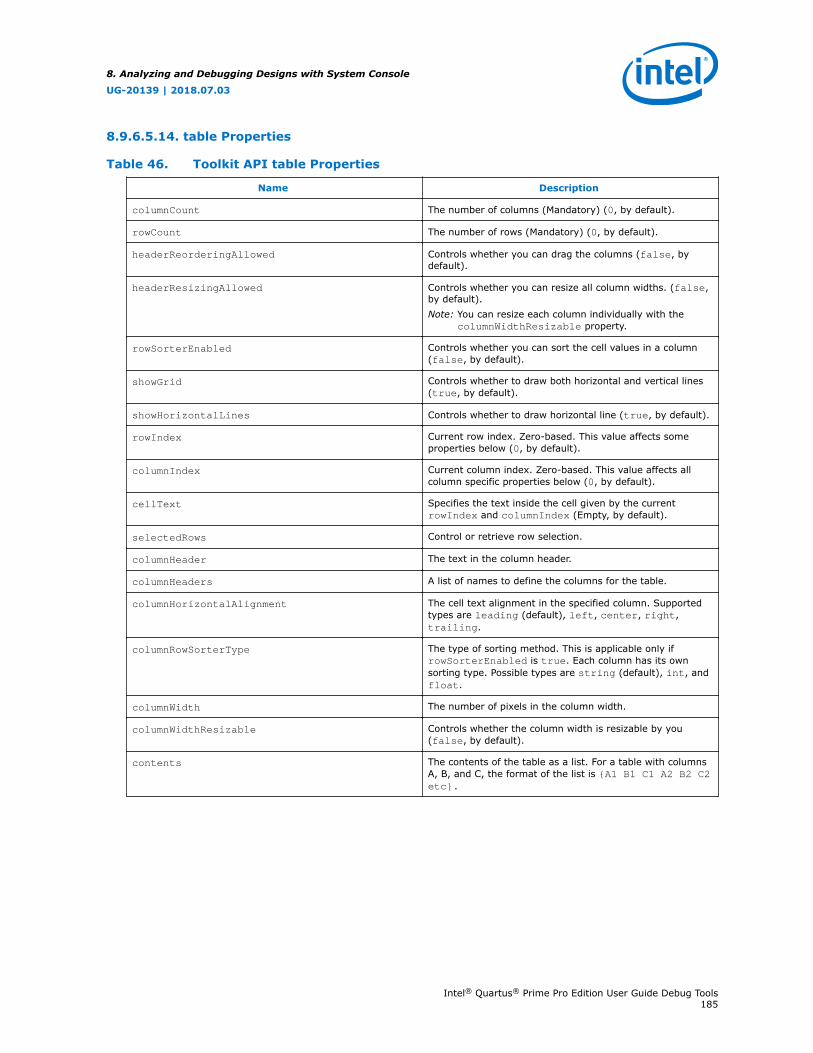
8.9.6.5.14. table Properties
Table 46. Toolkit API table Properties
Name Description
columnCount The number of columns (Mandatory) (0, by default).
rowCount The number of rows (Mandatory) (0, by default).
headerReorderingAllowed Controls whether you can drag the columns (false, bydefault).
headerResizingAllowed Controls whether you can resize all column widths. (false,by default).Note: You can resize each column individually with the
columnWidthResizable property.
rowSorterEnabled Controls whether you can sort the cell values in a column(false, by default).
showGrid Controls whether to draw both horizontal and vertical lines(true, by default).
showHorizontalLines Controls whether to draw horizontal line (true, by default).
rowIndex Current row index. Zero-based. This value affects someproperties below (0, by default).
columnIndex Current column index. Zero-based. This value affects allcolumn specific properties below (0, by default).
cellText Specifies the text inside the cell given by the currentrowIndex and columnIndex (Empty, by default).
selectedRows Control or retrieve row selection.
columnHeader The text in the column header.
columnHeaders A list of names to define the columns for the table.
columnHorizontalAlignment The cell text alignment in the specified column. Supportedtypes are leading (default), left, center, right,trailing.
columnRowSorterType The type of sorting method. This is applicable only ifrowSorterEnabled is true. Each column has its ownsorting type. Possible types are string (default), int, andfloat.
columnWidth The number of pixels in the column width.
columnWidthResizable Controls whether the column width is resizable by you(false, by default).
contents The contents of the table as a list. For a table with columnsA, B, and C, the format of the list is {A1 B1 C1 A2 B2 C2etc}.
8. Analyzing and Debugging Designs with System Console
UG-20139 | 2018.07.03
Intel® Quartus® Prime Pro Edition User Guide Debug Tools185

8.9.6.5.15. text Properties
Table 47. Toolkit API text Properties
Name Description
editable Controls whether the text box is editable.
htmlCapable Controls whether the text box can format HTML.
text The text to show in the text box.
8. Analyzing and Debugging Designs with System Console
UG-20139 | 2018.07.03
Intel® Quartus® Prime Pro Edition User Guide Debug Tools186

8.9.6.5.16. textField Properties
Table 48. Toolkit API textField Properties
Name Description
editable Controls whether the text box is editable.
onChange A Tcl callback to run when you change the content of thetext box.
text The text in the text box.
8. Analyzing and Debugging Designs with System Console
UG-20139 | 2018.07.03
Intel® Quartus® Prime Pro Edition User Guide Debug Tools187
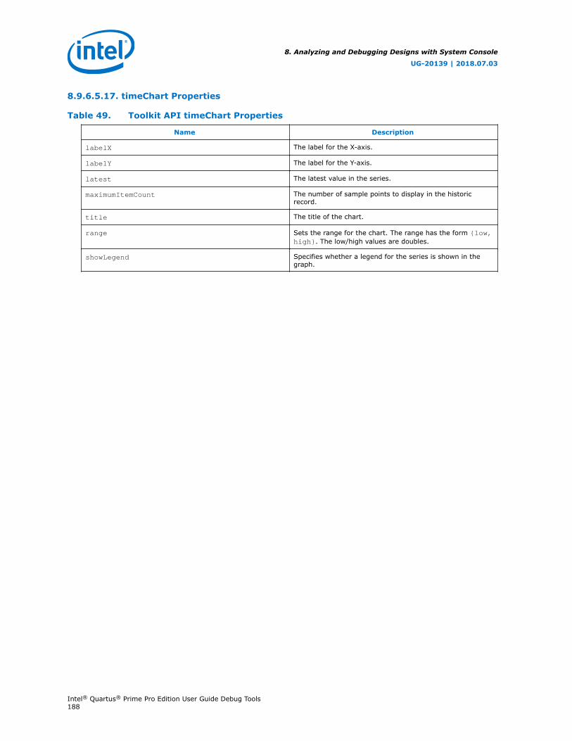
8.9.6.5.17. timeChart Properties
Table 49. Toolkit API timeChart Properties
Name Description
labelX The label for the X-axis.
labelY The label for the Y-axis.
latest The latest value in the series.
maximumItemCount The number of sample points to display in the historicrecord.
title The title of the chart.
range Sets the range for the chart. The range has the form {low,high}. The low/high values are doubles.
showLegend Specifies whether a legend for the series is shown in thegraph.
8. Analyzing and Debugging Designs with System Console
UG-20139 | 2018.07.03
Intel® Quartus® Prime Pro Edition User Guide Debug Tools188
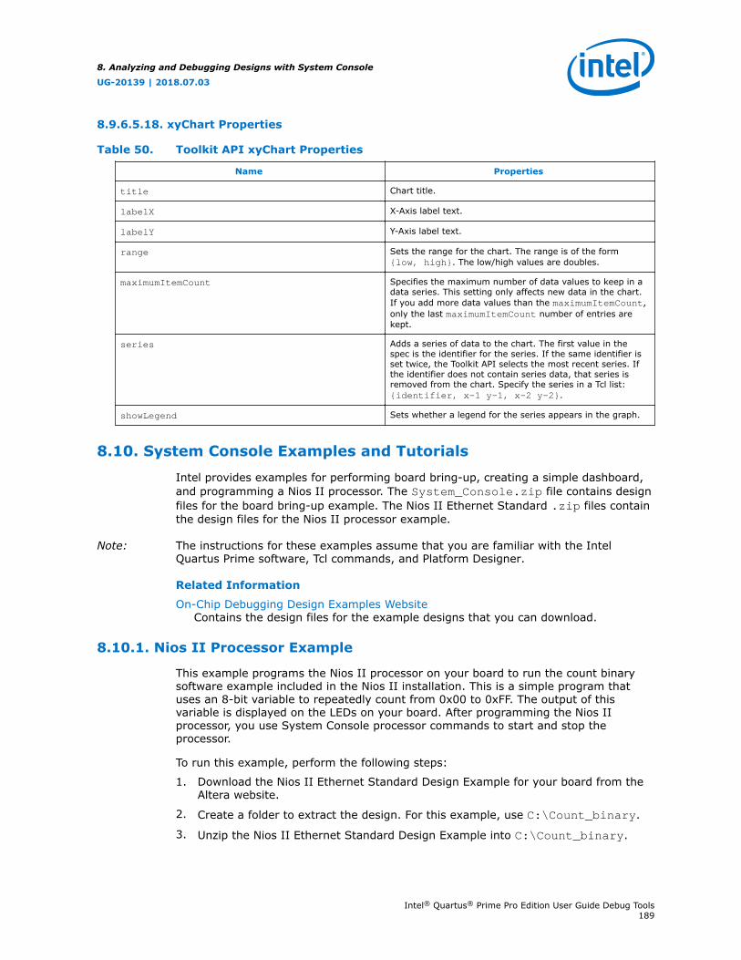
8.9.6.5.18. xyChart Properties
Table 50. Toolkit API xyChart Properties
Name Properties
title Chart title.
labelX X-Axis label text.
labelY Y-Axis label text.
range Sets the range for the chart. The range is of the form{low, high}. The low/high values are doubles.
maximumItemCount Specifies the maximum number of data values to keep in adata series. This setting only affects new data in the chart.If you add more data values than the maximumItemCount,only the last maximumItemCount number of entries arekept.
series Adds a series of data to the chart. The first value in thespec is the identifier for the series. If the same identifier isset twice, the Toolkit API selects the most recent series. Ifthe identifier does not contain series data, that series isremoved from the chart. Specify the series in a Tcl list:{identifier, x-1 y-1, x-2 y-2}.
showLegend Sets whether a legend for the series appears in the graph.
8.10. System Console Examples and Tutorials
Intel provides examples for performing board bring-up, creating a simple dashboard,and programming a Nios II processor. The System_Console.zip file contains designfiles for the board bring-up example. The Nios II Ethernet Standard .zip files containthe design files for the Nios II processor example.
Note: The instructions for these examples assume that you are familiar with the IntelQuartus Prime software, Tcl commands, and Platform Designer.
Related Information
On-Chip Debugging Design Examples WebsiteContains the design files for the example designs that you can download.
8.10.1. Nios II Processor Example
This example programs the Nios II processor on your board to run the count binarysoftware example included in the Nios II installation. This is a simple program thatuses an 8-bit variable to repeatedly count from 0x00 to 0xFF. The output of thisvariable is displayed on the LEDs on your board. After programming the Nios IIprocessor, you use System Console processor commands to start and stop theprocessor.
To run this example, perform the following steps:
1. Download the Nios II Ethernet Standard Design Example for your board from theAltera website.
2. Create a folder to extract the design. For this example, use C:\Count_binary.
3. Unzip the Nios II Ethernet Standard Design Example into C:\Count_binary.
8. Analyzing and Debugging Designs with System Console
UG-20139 | 2018.07.03
Intel® Quartus® Prime Pro Edition User Guide Debug Tools189
4. In a Nios II command shell, change to the directory of your new project.
5. Program your board. In a Nios II command shell, type the following:
nios2-configure-sof niosii_ethernet_standard_<board_version>.sof
6. Using Nios II Software Build Tools for Eclipse, create a new Nios II Application andBSP from Template using the Count Binary template and targeting the Nios IIEthernet Standard Design Example.
7. To build the executable and linkable format (ELF) file (.elf) for this application,right-click the Count Binary project and select Build Project.
8. Download the .elf file to your board by right-clicking Count Binary project andselecting Run As, Nios II Hardware.
• The LEDs on your board provide a new light show.
9. Type the following:
system-console; #Start System Console.
#Set the processor service path to the Nios II processor.set niosii_proc [lindex [get_service_paths processor] 0]
set claimed_proc [claim_service processor $niosii_proc mylib]; #Open the service.
processor_stop $claimed_proc; #Stop the processor.#The LEDs on your board freeze.
processor_run $claimed_proc; #Start the processor.#The LEDs on your board resume their previous activity.
processor_stop $claimed_proc; #Stop the processor.
close_service processor $claimed_proc; #Close the service.
• The processor_step, processor_set_register, andprocessor_get_register commands provide additional control over theNios II processor.
Related Information
• Nios II Ethernet Standard Design Example
• Nios II Gen2 Software Developer's Handbook
8. Analyzing and Debugging Designs with System Console
UG-20139 | 2018.07.03
Intel® Quartus® Prime Pro Edition User Guide Debug Tools190
8.10.1.1. Processor Commands
Table 51. Processor Commands
Command (1) Arguments Function
processor_download_elf <service-path><elf-file-path>
Downloads the given Executable and Linking Format File(.elf) to memory using the master service associated with theprocessor. Sets the processor's program counter to the .elfentry point.
processor_in_debug_mode <service-path> Returns a non-zero value if the processor is in debug mode.
processor_reset <service-path> Resets the processor and places it in debug mode.
processor_run <service-path> Puts the processor into run mode.
processor_stop <service-path> Puts the processor into debug mode.
processor_step <service-path> Executes one assembly instruction.
processor_get_register_names <service-path> Returns a list with the names of all of the processor's accessibleregisters.
processor_get_register <service-path><register_name>
Returns the value of the specified register.
processor_set_register <service-path><register_name><value>
Sets the value of the specified register.
Related Information
Nios II Processor Example on page 189
8.11. On-Board Intel FPGA Download Cable II Support
System Console supports an On-Board Intel FPGA Download Cable II circuit via theUSB Debug Master IP component. This IP core supports the master service.
8.12. MATLAB and Simulink* in a System Verification Flow
You can test system development in System Console using MATLAB and Simulink*,and set up a system verification flow using the Intel FPGA Hardware in the Loop (HIL)tools. In this approach, you deploy the design hardware to run in real time, andsimulate the system's surrounding components in a software environment. The HILapproach allows you to use the flexibility of software tools with the real-worldaccuracy and speed of hardware. You can gradually introduce more hardwarecomponents to the system verification testbench. This technique gives you morecontrol over the integration process as you tune and validate the system. When thefull system is integrated, the HIL approach allows you to provide stimuli via softwareto test the system under a variety of scenarios.
(1) If your system includes a Nios II/f core with a data cache, it may complicate the debuggingprocess. If you suspect the Nios II/f core writes to memory from the data cache atnondeterministic intervals; thereby, overwriting data written by the System Console, you candisable the cache of the Nios II/f core while debugging.
8. Analyzing and Debugging Designs with System Console
UG-20139 | 2018.07.03
Intel® Quartus® Prime Pro Edition User Guide Debug Tools191
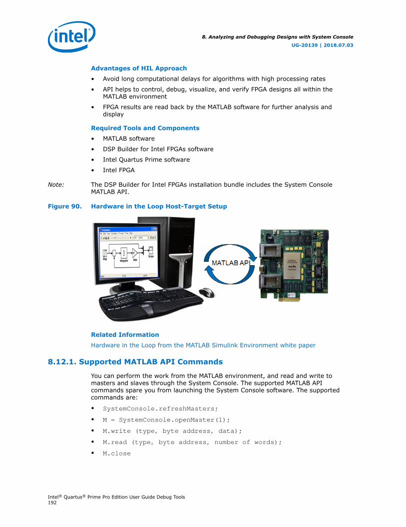
Advantages of HIL Approach
• Avoid long computational delays for algorithms with high processing rates
• API helps to control, debug, visualize, and verify FPGA designs all within theMATLAB environment
• FPGA results are read back by the MATLAB software for further analysis anddisplay
Required Tools and Components
• MATLAB software
• DSP Builder for Intel FPGAs software
• Intel Quartus Prime software
• Intel FPGA
Note: The DSP Builder for Intel FPGAs installation bundle includes the System ConsoleMATLAB API.
Figure 90. Hardware in the Loop Host-Target Setup
Related Information
Hardware in the Loop from the MATLAB Simulink Environment white paper
8.12.1. Supported MATLAB API Commands
You can perform the work from the MATLAB environment, and read and write tomasters and slaves through the System Console. The supported MATLAB APIcommands spare you from launching the System Console software. The supportedcommands are:
• SystemConsole.refreshMasters;
• M = SystemConsole.openMaster(1);
• M.write (type, byte address, data);
• M.read (type, byte address, number of words);
• M.close
8. Analyzing and Debugging Designs with System Console
UG-20139 | 2018.07.03
Intel® Quartus® Prime Pro Edition User Guide Debug Tools192

Example 31. MATLAB API Script Example
SystemConsole.refreshMasters; %Investigate available targetsM = SystemConsole.openMaster(1); %Creates connection with FPGA target%%%%%%%% User Application %%%%%%%%%%%%....M.write('uint32',write_address,data); %Send data to FPGA target....data = M.read('uint32',read_address,size); %Read data from FPGA target....%%%%%%%%%%%%%%%%%%%%%%%%%%%%%%%%%%%%%%M.close; %Terminates connection to FPGA target
8.12.2. High Level Flow
1. Install the DSP Builder for Intel FPGAs software, so you have the necessarylibraries to enable this flow
2. Build the design using Simulink and the DSP Builder for Intel FPGAs libraries.
DSP Builder for Intel FPGAs helps to convert the Simulink design to HDL
3. Include Avalon-MM components in the design (DSP Builder for Intel FPGAs canport non-Avalon-MM components)
4. Include Signals and Control blocks in the design
5. Separate synthesizable and non-synthesizable logic with boundary blocks.
6. Integrate the DSP system in Platform Designer
7. Program the Intel FPGA
8. Interact with the Intel FPGA through the supported MATLAB API commands.
8.13. Deprecated Commands
The table lists commands that have been deprecated. These commands are currentlysupported, but are targeted for removal from System Console.
Note: All dashboard_<name> commands are deprecated and replaced withtoolkit_<name> commands for Intel Quartus Prime software15.1, and later.
Table 52. Deprecated Commands
Command Arguments Function
open_service <service_type><service_path>
Opens the specified service type at the specified path.Calls to open_service may be replaced with calls to claim_service providing thatthe return value from claim_service is stored and used to access and close theservice.
8. Analyzing and Debugging Designs with System Console
UG-20139 | 2018.07.03
Intel® Quartus® Prime Pro Edition User Guide Debug Tools193
8.14. Analyzing and Debugging Designs with System ConsoleRevision History
Document Version Intel QuartusPrime Version
Changes
2018.05.07 18.0.0 Removed obsolete section: Board Bring-Up with System Console Tutorial.
2017.05.08 17.0.0 • Created topic Convert your Dashboard Scripts to Toolkit API.• Removed Registering the Service Example from Toolkit API Script
Examples, and added corresponding code snippet to Registering aToolkit.
• Moved .toolkit Description File Example under Creating a ToolkitDescription File.
• Renamed Toolkit API GUI Example .toolkit File to .toolkit DescriptionFile Example.
• Updated examples on Toolkit API to reflect current supported syntax.
2016.10.31 16.1.0 • Implemented Intel rebranding.
2015.11.02 15.1.0 • Edits to Toolkit API content and command format.• Added Toolkit API design example.• Added graphic to Introduction to System Console.• Deprecated Dashboard.• Changed instances of Quartus II to Intel Quartus Prime.
October 2015 15.1.0 • Added content for Toolkit API— Required .toolkit and Tcl files— Registering and launching the toolkit— Toolkit discovery and matching toolkits to IP— Toolkit API commands table
May 2015 15.0.0 Added information about how to download and start System Consolestand-alone.
December 2014 14.1.0 • Added overview and procedures for using ADC Toolkit on MAX 10devices.
• Added overview for using MATLAB/Simulink Environment with SystemConsole for system verification.
June 2014 14.0.0 Updated design examples for the following: board bring-up, dashboardservice, Nios II processor, design service, device service, monitor service,bytestream service, SLD service, and ISSP service.
November 2013 13.1.0 Re-organization of sections. Added high-level information with blockdiagram, workflow, SLD overview, use cases, and example Tcl scripts.
June 2013 13.0.0 Updated Tcl command tables. Added board bring-up design example.Removed SOPC Builder content.
November 2012 12.1.0 Re-organization of content.
August 2012 12.0.1 Moved Transceiver Toolkit commands to Transceiver Toolkit chapter.
June 2012 12.0.0 Maintenance release. This chapter adds new System Console features.
November 2011 11.1.0 Maintenance release. This chapter adds new System Console features.
May 2011 11.0.0 Maintenance release. This chapter adds new System Console features.
December 2010 10.1.0 Maintenance release. This chapter adds new commands and references forQsys.
July 2010 10.0.0 Initial release. Previously released as the System Console User Guide,which is being obsoleted. This new chapter adds new commands.
8. Analyzing and Debugging Designs with System Console
UG-20139 | 2018.07.03
Intel® Quartus® Prime Pro Edition User Guide Debug Tools194

Related Information
Documentation ArchiveFor previous versions of the Intel Quartus Prime Handbook, search thedocumentation archives.
8. Analyzing and Debugging Designs with System Console
UG-20139 | 2018.07.03
Intel® Quartus® Prime Pro Edition User Guide Debug Tools195

9. Debugging Transceiver LinksThe Transceiver Toolkit helps you optimize high-speed serial links in your board designby providing real-time control, monitoring, and debugging of the transceiver linksrunning on your board.
The Transceiver Toolkit allows you to:
• Control the transmitter or receiver channels to optimize transceiver settings andhardware features.
• Test bit-error rate (BER) while running multiple links at the target data rate.
• Control internal pattern generators and checkers, as well as enabling loopbackmodes.
• Run auto sweep tests to identify the best physical media attachment (PMA)settings for each link.
• For Intel Stratix 10 devices, view the receiver horizontal and vertical eye marginduring testing.
• Test multiple devices across multiple boards simultaneously.
Note: The Transceiver Toolkit runs from the System Console framework.
To launch the toolkit, click Tools ➤ System Debugging Tools ➤ TransceiverToolkit. Alternatively, you can run Tcl scripts from the command-line:
system-console --script=<name of script>
For an online demonstration using the Transceiver Toolkit to run a high-speed link testwith one of the design examples, refer to the Transceiver Toolkit Online Demo on theAltera website.
Related Information
• Transceiver Design Examples and Reference Designs
• Transceiver Toolkit Online Demo
• Transceiver Toolkit for Intel Arria 10 Devices (OTCVRKITA10)26 Minutes Online Course
9.1. Device Support
The Intel Quartus Prime Pro Edition Transceiver Toolkit supports the following devicefamilies:
• Intel Arria 10
• Intel Cyclone 10 GX
• Intel Stratix 10 L-, H-, and E-Tile
UG-20139 | 2018.07.03
Intel Corporation. All rights reserved. Intel, the Intel logo, Altera, Arria, Cyclone, Enpirion, MAX, Nios, Quartusand Stratix words and logos are trademarks of Intel Corporation or its subsidiaries in the U.S. and/or othercountries. Intel warrants performance of its FPGA and semiconductor products to current specifications inaccordance with Intel's standard warranty, but reserves the right to make changes to any products and servicesat any time without notice. Intel assumes no responsibility or liability arising out of the application or use of anyinformation, product, or service described herein except as expressly agreed to in writing by Intel. Intelcustomers are advised to obtain the latest version of device specifications before relying on any publishedinformation and before placing orders for products or services.*Other names and brands may be claimed as the property of others.
ISO9001:2008Registered
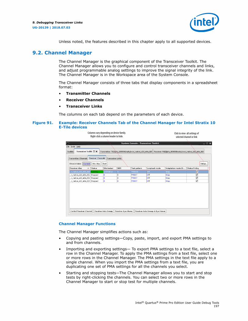
Unless noted, the features described in this chapter apply to all supported devices.
9.2. Channel Manager
The Channel Manager is the graphical component of the Transceiver Toolkit. TheChannel Manager allows you to configure and control transceiver channels and links,and adjust programmable analog settings to improve the signal integrity of the link.The Channel Manager is in the Workspace area of the System Console.
The Channel Manager consists of three tabs that display components in a spreadsheetformat:
• Transmitter Channels
• Receiver Channels
• Transceiver Links
The columns on each tab depend on the parameters of each device.
Figure 91. Example: Receiver Channels Tab of the Channel Manager for Intel Stratix 10E-Tile devices
Columns vary depending on device family.Right-click a column header to hide.
Click to view all settings ofselected channel or link
Channel Manager Functions
The Channel Manager simplifies actions such as:
• Copying and pasting settings—Copy, paste, import, and export PMA settings toand from channels.
• Importing and exporting settings— To export PMA settings to a text file, select arow in the Channel Manager. To apply the PMA settings from a text file, select oneor more rows in the Channel Manager. The PMA settings in the text file apply to asingle channel. When you import the PMA settings from a text file, you areduplicating one set of PMA settings for all the channels you select.
• Starting and stopping tests—The Channel Manager allows you to start and stoptests by right-clicking the channels. You can select two or more rows in theChannel Manager to start or stop test for multiple channels.
9. Debugging Transceiver Links
UG-20139 | 2018.07.03
Intel® Quartus® Prime Pro Edition User Guide Debug Tools197
Related Information
• System Explorer Pane on page 136
• System Console GUI on page 135
• User Interface Settings Reference on page 221
9.2.1. Channel Display Modes
The three channel display modes are:
• Current (default)—shows the current values from the device. Blue text indicatesthat the settings are live.
• Min/Max—shows the minimum and maximum values to be used in the autosweep.
• Best—shows the best tested values from the last completed auto sweep run.
Note: The Transmitter Channels tab only shows the Current display mode. TheTransceiver Toolkit requires a receiver channel to perform auto sweep tests.
9.3. Transceiver Debugging Flow Walkthrough
These steps describe the high-level process of debugging transceivers with theTransceiver Toolkit.
1. Modify the design to enable transceiver debug.
2. Load the modified design to the FPGA.
3. Load the design to the Transceiver Toolkit.
4. Link hardware resources.
5. Verify hardware connections.
6. Identify transceiver channels.
7. Run link tests or control PMA analog settings.
9.4. Modifying the Design to Enable Transceiver Debug
To enable debugging capabilities, you must change parameters of one or moretransceiver Intel FPGA IP Cores.
Related Information
Device Support on page 196
9. Debugging Transceiver Links
UG-20139 | 2018.07.03
Intel® Quartus® Prime Pro Edition User Guide Debug Tools198
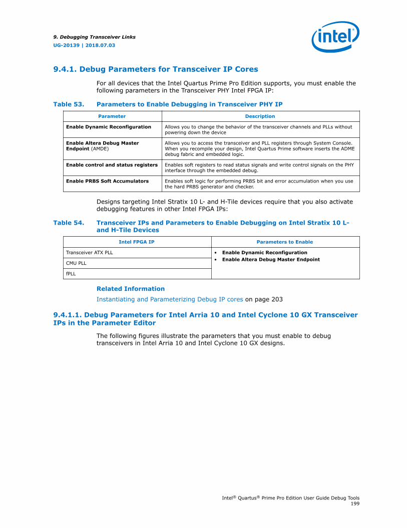
9.4.1. Debug Parameters for Transceiver IP Cores
For all devices that the Intel Quartus Prime Pro Edition supports, you must enable thefollowing parameters in the Transceiver PHY Intel FPGA IP:
Table 53. Parameters to Enable Debugging in Transceiver PHY IP
Parameter Description
Enable Dynamic Reconfiguration Allows you to change the behavior of the transceiver channels and PLLs withoutpowering down the device
Enable Altera Debug MasterEndpoint (AMDE)
Allows you to access the transceiver and PLL registers through System Console.When you recompile your design, Intel Quartus Prime software inserts the ADMEdebug fabric and embedded logic.
Enable control and status registers Enables soft registers to read status signals and write control signals on the PHYinterface through the embedded debug.
Enable PRBS Soft Accumulators Enables soft logic for performing PRBS bit and error accumulation when you usethe hard PRBS generator and checker.
Designs targeting Intel Stratix 10 L- and H-Tile devices require that you also activatedebugging features in other Intel FPGA IPs:
Table 54. Transceiver IPs and Parameters to Enable Debugging on Intel Stratix 10 L-and H-Tile Devices
Intel FPGA IP Parameters to Enable
Transceiver ATX PLL • Enable Dynamic Reconfiguration• Enable Altera Debug Master Endpoint
CMU PLL
fPLL
Related Information
Instantiating and Parameterizing Debug IP cores on page 203
9.4.1.1. Debug Parameters for Intel Arria 10 and Intel Cyclone 10 GX TransceiverIPs in the Parameter Editor
The following figures illustrate the parameters that you must enable to debugtransceivers in Intel Arria 10 and Intel Cyclone 10 GX designs.
9. Debugging Transceiver Links
UG-20139 | 2018.07.03
Intel® Quartus® Prime Pro Edition User Guide Debug Tools199
Figure 92. Dynamic Reconfiguration Parameters in Intel Arria 10 and Intel Cyclone 10GX Transceiver Native PHY IP Core
Figure 93. Dynamic Reconfiguration Parameters in Intel Arria 10 and Intel Cyclone 10GX Transceiver ATX PLL Core
For more information about dynamic reconfiguration parameters in Intel Arria 10devices, refer to the Intel Arria 10 Transceiver PHY User Guide.
For more information about dynamic reconfiguration parameters in Intel Cyclone 10GX devices, refer to the Intel Cyclone 10 GX Transceiver PHY User Guide.
Related Information
• Dynamic Reconfiguration ParametersIn Intel Arria 10 Transceiver PHY User Guide
• Reconfiguration Interface and Dynamic ReconfigurationIn Intel Cyclone 10 GX Transceiver PHY User Guide
9. Debugging Transceiver Links
UG-20139 | 2018.07.03
Intel® Quartus® Prime Pro Edition User Guide Debug Tools200
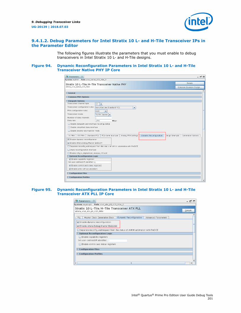
9.4.1.2. Debug Parameters for Intel Stratix 10 L- and H-Tile Transceiver IPs inthe Parameter Editor
The following figures illustrate the parameters that you must enable to debugtransceivers in Intel Stratix 10 L- and H-Tile designs.
Figure 94. Dynamic Reconfiguration Parameters in Intel Stratix 10 L- and H-TileTransceiver Native PHY IP Core
Figure 95. Dynamic Reconfiguration Parameters in Intel Stratix 10 L- and H-TileTransceiver ATX PLL IP Core
9. Debugging Transceiver Links
UG-20139 | 2018.07.03
Intel® Quartus® Prime Pro Edition User Guide Debug Tools201
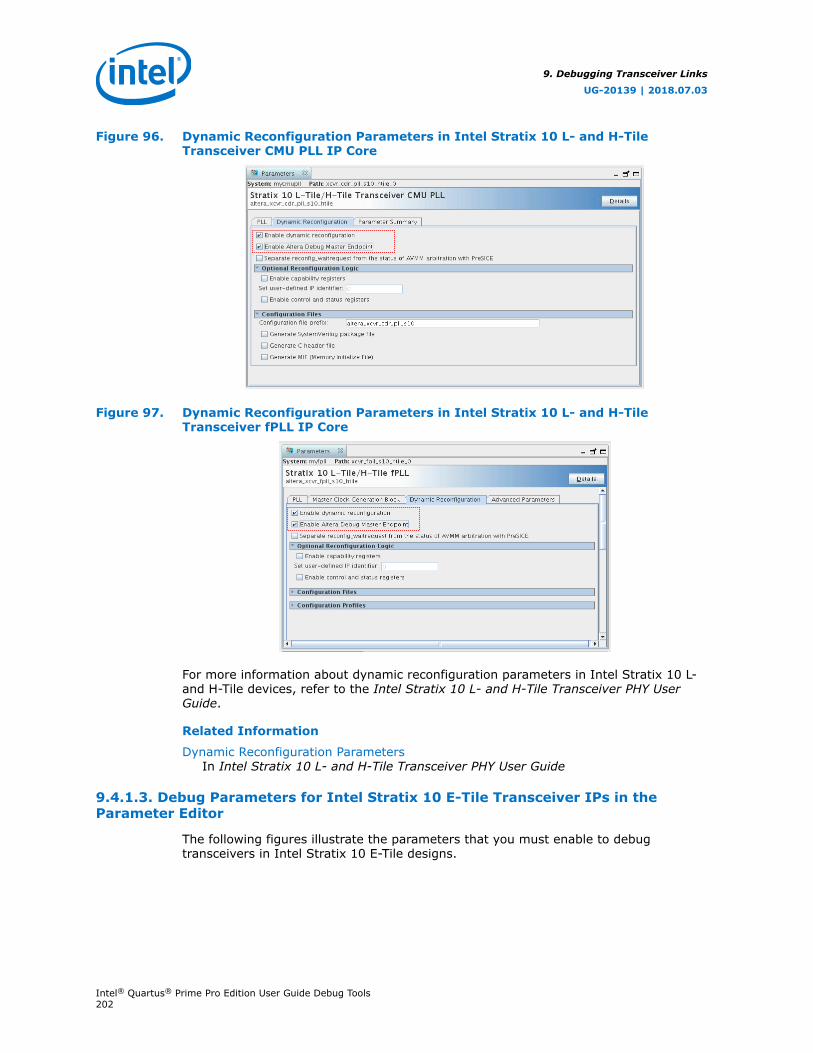
Figure 96. Dynamic Reconfiguration Parameters in Intel Stratix 10 L- and H-TileTransceiver CMU PLL IP Core
Figure 97. Dynamic Reconfiguration Parameters in Intel Stratix 10 L- and H-TileTransceiver fPLL IP Core
For more information about dynamic reconfiguration parameters in Intel Stratix 10 L-and H-Tile devices, refer to the Intel Stratix 10 L- and H-Tile Transceiver PHY UserGuide.
Related Information
Dynamic Reconfiguration ParametersIn Intel Stratix 10 L- and H-Tile Transceiver PHY User Guide
9.4.1.3. Debug Parameters for Intel Stratix 10 E-Tile Transceiver IPs in theParameter Editor
The following figures illustrate the parameters that you must enable to debugtransceivers in Intel Stratix 10 E-Tile designs.
9. Debugging Transceiver Links
UG-20139 | 2018.07.03
Intel® Quartus® Prime Pro Edition User Guide Debug Tools202
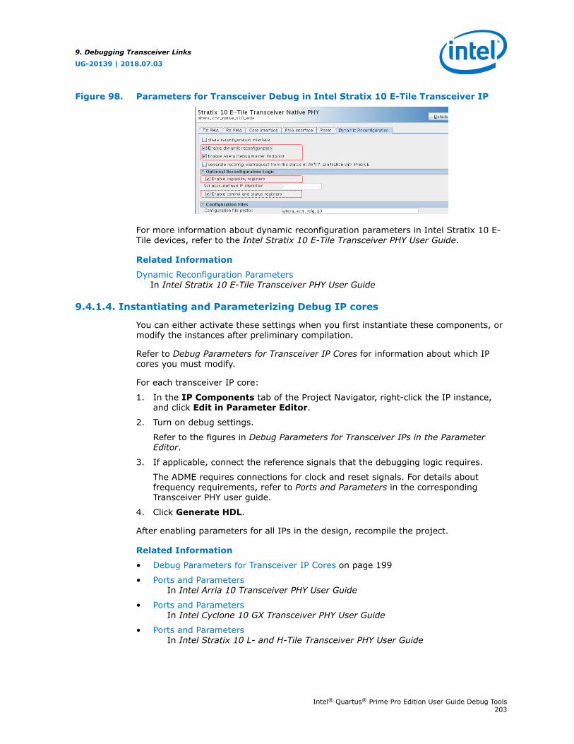
Figure 98. Parameters for Transceiver Debug in Intel Stratix 10 E-Tile Transceiver IP
For more information about dynamic reconfiguration parameters in Intel Stratix 10 E-Tile devices, refer to the Intel Stratix 10 E-Tile Transceiver PHY User Guide.
Related Information
Dynamic Reconfiguration ParametersIn Intel Stratix 10 E-Tile Transceiver PHY User Guide
9.4.1.4. Instantiating and Parameterizing Debug IP cores
You can either activate these settings when you first instantiate these components, ormodify the instances after preliminary compilation.
Refer to Debug Parameters for Transceiver IP Cores for information about which IPcores you must modify.
For each transceiver IP core:
1. In the IP Components tab of the Project Navigator, right-click the IP instance,and click Edit in Parameter Editor.
2. Turn on debug settings.
Refer to the figures in Debug Parameters for Transceiver IPs in the ParameterEditor.
3. If applicable, connect the reference signals that the debugging logic requires.
The ADME requires connections for clock and reset signals. For details aboutfrequency requirements, refer to Ports and Parameters in the correspondingTransceiver PHY user guide.
4. Click Generate HDL.
After enabling parameters for all IPs in the design, recompile the project.
Related Information
• Debug Parameters for Transceiver IP Cores on page 199
• Ports and ParametersIn Intel Arria 10 Transceiver PHY User Guide
• Ports and ParametersIn Intel Cyclone 10 GX Transceiver PHY User Guide
• Ports and ParametersIn Intel Stratix 10 L- and H-Tile Transceiver PHY User Guide
9. Debugging Transceiver Links
UG-20139 | 2018.07.03
Intel® Quartus® Prime Pro Edition User Guide Debug Tools203

• Ports and ParametersIn Intel Stratix 10 E-Tile Transceiver PHY User Guide
9.5. Programming the Design into an Intel FPGA
After you include debug components in the design, compile, and generateprogramming files, you can program the design in the Intel FPGA.
Related Information
Programming Intel FPGA DevicesIn Programmer User Guide: Intel Quartus Prime Pro Edition
9.6. Loading the Design in the Transceiver Toolkit
If the FPGA is already programmed with the project when loading, the TransceiverToolkit automatically links the design to the target hardware in the toolkit. The toolkitautomatically discovers links between transmitter and receiver of the same channel.
Before loading the device, ensure that you connect the hardware. The device and JTAGconnections appear in the Device and Connections folders of the System Explorerpane.
To load the design into the Transceiver Toolkit:
1. In the System Console, click File ➤ Load Design.
2. Select the .sof programming file for the transceiver design.
After loading the project, the designs and design instances folders in the SystemExplorer pane display information about the design, such as the design name and theblocks in the design that can communicate to the System Console.
Related Information
System Explorer Pane on page 136
9.7. Linking Hardware Resources
Linking the hardware resources maps the project you load to the target FPGA. Whenyou load multiple design projects for multiple FPGAs, linking indicates which of theprojects is in each of the FPGAs. The toolkit automatically discovers hardware anddesigns that you connect. You can also manually link a design to connected hardwareresources in the System Explorer.
If you are using more than one Intel FPGA board, you can set up a test with multipledevices linked to the same design. This setup is useful if you want to perform a linktest between a transmitter and receiver on two separate devices. You can also loadmultiple Intel Quartus Prime projects and link between different systems. You canperform tests on separate and unrelated systems in a single Intel Quartus Primeinstance.
9. Debugging Transceiver Links
UG-20139 | 2018.07.03
Intel® Quartus® Prime Pro Edition User Guide Debug Tools204
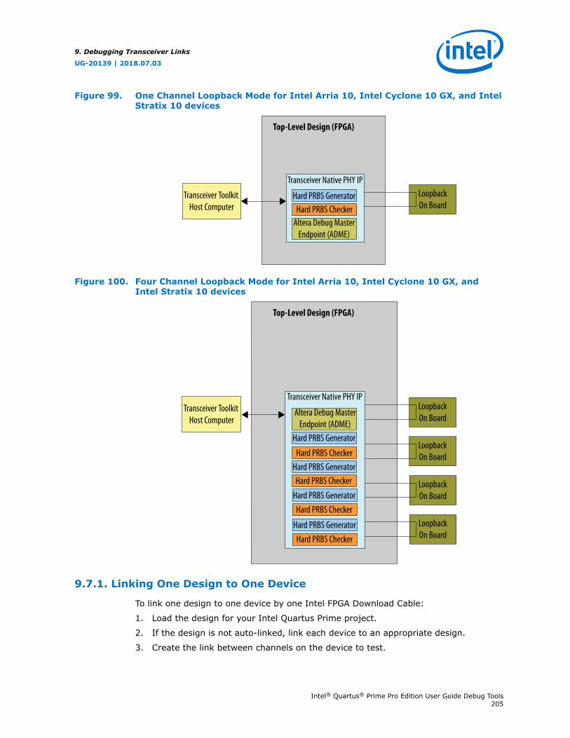
Figure 99. One Channel Loopback Mode for Intel Arria 10, Intel Cyclone 10 GX, and IntelStratix 10 devices
Transceiver ToolkitHost Computer
Top-Level Design (FPGA)
LoopbackOn Board
Hard PRBS GeneratorHard PRBS Checker
Altera Debug MasterEndpoint (ADME)
Transceiver Native PHY IP
Figure 100. Four Channel Loopback Mode for Intel Arria 10, Intel Cyclone 10 GX, andIntel Stratix 10 devices
Transceiver ToolkitHost Computer
Top-Level Design (FPGA)
LoopbackOn Board
Hard PRBS Generator
Hard PRBS Checker
Altera Debug MasterEndpoint (ADME)
Transceiver Native PHY IP
LoopbackOn Board
Hard PRBS GeneratorHard PRBS Checker Loopback
On BoardHard PRBS GeneratorHard PRBS Checker
LoopbackOn Board
Hard PRBS GeneratorHard PRBS Checker
9.7.1. Linking One Design to One Device
To link one design to one device by one Intel FPGA Download Cable:
1. Load the design for your Intel Quartus Prime project.
2. If the design is not auto-linked, link each device to an appropriate design.
3. Create the link between channels on the device to test.
9. Debugging Transceiver Links
UG-20139 | 2018.07.03
Intel® Quartus® Prime Pro Edition User Guide Debug Tools205

9.7.2. Linking Two Designs to Two Devices
To link two designs to two separate devices on the same board, connected by oneIntel FPGA Download Cable download cable:
1. Load the design for all the Intel Quartus Prime project files you need.
2. If the design does not auto-link, link each device to an appropriate design
3. Open the project for the second device.
4. Link the second device on the JTAG chain to the second design (unless the designauto-links).
5. Create a link between the channels on the devices you want to test.
9.7.3. Linking One Design on Two Devices
To link the same design on two separate devices, follow these steps:
1. In the Transceiver Toolkit, open the .sof you are using on both devices.
2. Link the first device to this design instance.
3. Link the second device to the design.
4. Create a link between the channels on the devices you want to test.
9.7.4. Linking Designs and Devices on Separate Boards
To link two designs to two separate devices on separate boards that connect toseparate Intel FPGA Download Cables:
1. Load the design for all the Intel Quartus Prime project files you need.
2. If the design does not auto-link, link each device to an appropriate design.
3. Create the link between channels on the device to test.
4. Link the device connected to the second Intel FPGA Download Cable to the seconddesign.
5. Create a link between the channels on the devices you want to test.
9.7.5. Verifying Hardware Connections
After creating links, verify that the channels connect correctly and loop back properlyon the hardware.This precaution saves time in the workflow.
Use the toolkit to send data patterns and receive them correctly:
1. In the Receiver tab, verify that RX CDR locked to Data is set to Locked.
9. Debugging Transceiver Links
UG-20139 | 2018.07.03
Intel® Quartus® Prime Pro Edition User Guide Debug Tools206

Figure 101. RX CDR Locked to Data
2. Start the generator on the Transmitter Channel.
3. Start the checker on the Receiver Channel.
4. Verify you have Lock to Data, and the Bit Error Rate between the two is very lowor zero.
After you verify communication between transmitter and receiver, you can create alink between the two transceivers and perform Auto Sweep and Eye Viewer(2) testswith the pair.
9.8. Identifying Transceiver Channels
Verify whether the Transceiver Toolkit detects the channels correctly. If a receiver andtransmitter share a transceiver channel, the toolkit identifies the channel.
The Transceiver Toolkit identifies and displays transmitter and receiver channels on theTransmitter Channels and Receiver Channels tabs of the Channel Manager. Youcan also manually identify the transmitter and receiver in a transceiver channel, andthen create a link between the two for testing.
9.8.1. Controlling Transceiver Channels
To adjust or monitor transmitter or receiver settings while the channels are running:
• In the Transmitter Channels tab, click Control Transmitter Channel
• In the Receiver Channels tab, click Control Receiver Channel.
• In the Transceiver Links tab, click Control Receiver Channel.
For example, you can transmit a data pattern across the transceiver link, and thenreport the signal quality of the data you receive.
9.9. Creating Transceiver Links
Creating a link designates which Transmitter and Receiver channels connect physically.The toolkit automatically creates links when a receiver and transmitter share atransceiver channel. You can also manually create and delete links betweentransmitter and receiver channels.
(2) Eye Viewer available only for Intel Stratix 10 devices.
9. Debugging Transceiver Links
UG-20139 | 2018.07.03
Intel® Quartus® Prime Pro Edition User Guide Debug Tools207
To create a transceiver link:
1. In the Channel Manager, click Setup.
2. Select the generator and checker you want to control.
3. Select the transmitter and receiver pair you want to control.
4. Click Create Transceiver Link.
5. Click Close.
The Transceiver Toolkit generates an automatic name for the link, but you can use ashorter, more meaningful name by typing in the Link Alias cell.
9.10. Running Link Tests
Once you identify the transceiver channels for debugging, you can run link tests. Usethe Transceiver Links tab to control link tests.
When you run link tests, channel color highlights indicate the test status:
Table 55. Channel Color Highlights
Color Transmitter Channel Receiver Channel
Red Channel is closed or generator clock is notrunning.
Channel is closed or checker clock is not running.
Green Generator is sending a pattern. Checker is checking and data pattern is locked.
Neutral (same coloras background)
Channel is open, generator clock is running,and generator is not sending a pattern.
Channel is open, checker clock is running, andchecker is not checking.
Yellow N/A Checker is checking and data pattern is notlocked.
9.10.1. Running BER Tests
BER tests help you assess signal integrity. Different transceiver parameters result indifferent BER values.
You run BER tests from the Transceiver Link Basic tab.
9. Debugging Transceiver Links
UG-20139 | 2018.07.03
Intel® Quartus® Prime Pro Edition User Guide Debug Tools208
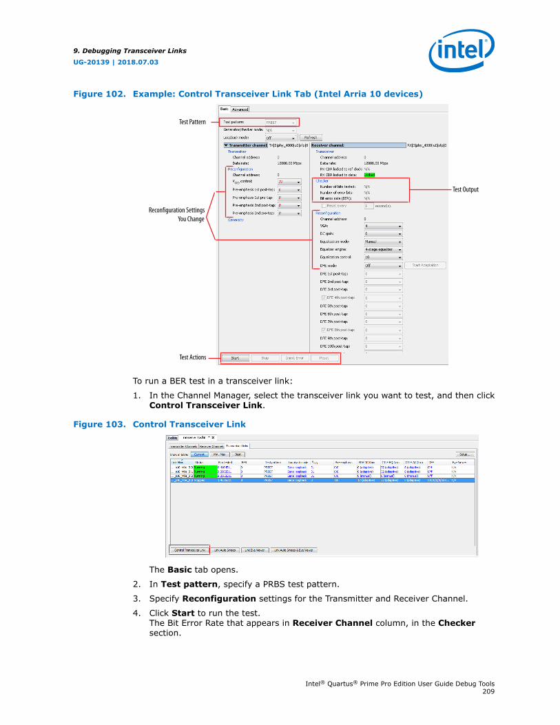
Figure 102. Example: Control Transceiver Link Tab (Intel Arria 10 devices)
Reconfiguration SettingsYou Change
Test Pattern
Test Actions
Test Output
To run a BER test in a transceiver link:
1. In the Channel Manager, select the transceiver link you want to test, and then clickControl Transceiver Link.
Figure 103. Control Transceiver Link
The Basic tab opens.
2. In Test pattern, specify a PRBS test pattern.
3. Specify Reconfiguration settings for the Transmitter and Receiver Channel.
4. Click Start to run the test.The Bit Error Rate that appears in Receiver Channel column, in the Checkersection.
9. Debugging Transceiver Links
UG-20139 | 2018.07.03
Intel® Quartus® Prime Pro Edition User Guide Debug Tools209
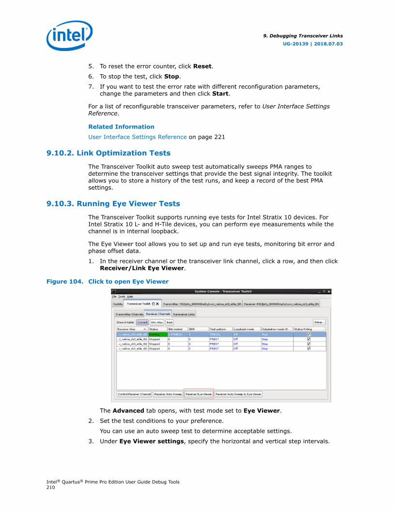
5. To reset the error counter, click Reset.
6. To stop the test, click Stop.
7. If you want to test the error rate with different reconfiguration parameters,change the parameters and then click Start.
For a list of reconfigurable transceiver parameters, refer to User Interface SettingsReference.
Related Information
User Interface Settings Reference on page 221
9.10.2. Link Optimization Tests
The Transceiver Toolkit auto sweep test automatically sweeps PMA ranges todetermine the transceiver settings that provide the best signal integrity. The toolkitallows you to store a history of the test runs, and keep a record of the best PMAsettings.
9.10.3. Running Eye Viewer Tests
The Transceiver Toolkit supports running eye tests for Intel Stratix 10 devices. ForIntel Stratix 10 L- and H-Tile devices, you can perform eye measurements while thechannel is in internal loopback.
The Eye Viewer tool allows you to set up and run eye tests, monitoring bit error andphase offset data.
1. In the receiver channel or the transceiver link channel, click a row, and then clickReceiver/Link Eye Viewer.
Figure 104. Click to open Eye Viewer
The Advanced tab opens, with test mode set to Eye Viewer.
2. Set the test conditions to your preference.
You can use an auto sweep test to determine acceptable settings.
3. Under Eye Viewer settings, specify the horizontal and vertical step intervals.
9. Debugging Transceiver Links
UG-20139 | 2018.07.03
Intel® Quartus® Prime Pro Edition User Guide Debug Tools210

4. Click Start.During the test, the Eye Viewer tool gathers the channel's current settings, anduses those settings to start a phase sweep.
5. Check the Eye Viewer status to see if the test finished.
6. To change PMA settings and run another test, click Stop, then Reset, and restartthe Eye Viewer test.
When the run completes, the Heat Map window appears, showing the results of thetest run.
Figure 105. Example: Result of an Eye Test for Design on Intel Stratix 10 E-Tile DeviceThis eye diagram corresponds to NRZ encoding. For information about characteristics of an Eye diagram fortransceivers with PAM4 encoding, refer to AN 835: PAM4 Signaling Fundamentals.
Note: Starting from Intel Quartus Prime version 18.0, you cannot import link test files fromearlier releases. Likewise, you cannot import reports generated in Intel Quartus Prime18.0 or later into earlier Quartus versions.
In the Advanced tab, click Create Report to view and export data to a table format.
9. Debugging Transceiver Links
UG-20139 | 2018.07.03
Intel® Quartus® Prime Pro Edition User Guide Debug Tools211

Figure 106. Example: Eye Test Report for Design on Intel Stratix 10 E-Tile Device
Related Information
• AN 835: PAM4 Signaling Fundamentals
• User Interface Settings Reference on page 221
9.11. Controlling PMA Analog Settings
The Transceiver Toolkit allows you to directly control PMA analog settings while the linkis running. For a detailed description of each parameter, refer to the PHY user guide ofthe corresponding device.
To control PMA analog settings, follow these steps:
1. In the Channel Manager, click Setup.
2. In the Transmitter Channels tab, define a transmitter without a generator, andclick Create Transmitter Channel.
3. In the Receiver Channels tab, define a receiver without a generator, and clickCreate Receiver Channel.
4. In the Transceiver Links tab, select the transmitter and receivers you want tocontrol, and click Create Transceiver Link.
5. Click Close.
6. Click Control Receiver Channel, Control Transmitter Channel, or ControlTransceiver Link to directly control the PMA settings while running.
9.11.1. Intel Arria 10 and Intel Cyclone 10 GX PMA Settings
The following figures show the PMA analog settings for Intel Arria 10 and Intel Cyclone10 GX devices.
9. Debugging Transceiver Links
UG-20139 | 2018.07.03
Intel® Quartus® Prime Pro Edition User Guide Debug Tools212
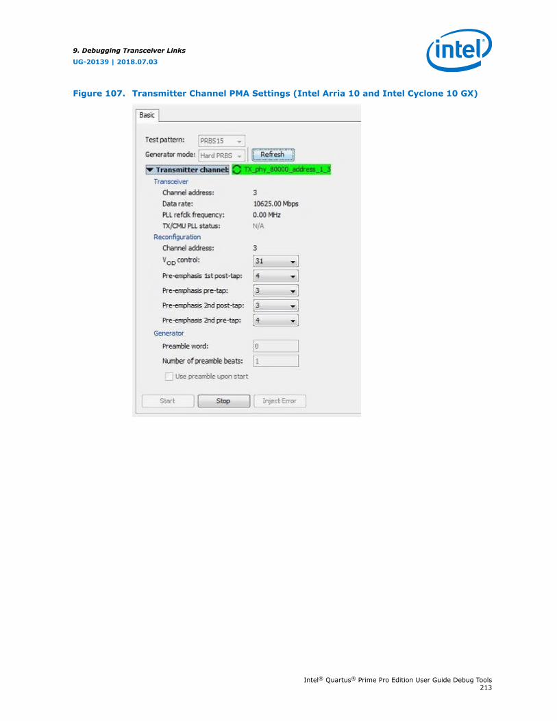
Figure 107. Transmitter Channel PMA Settings (Intel Arria 10 and Intel Cyclone 10 GX)
9. Debugging Transceiver Links
UG-20139 | 2018.07.03
Intel® Quartus® Prime Pro Edition User Guide Debug Tools213
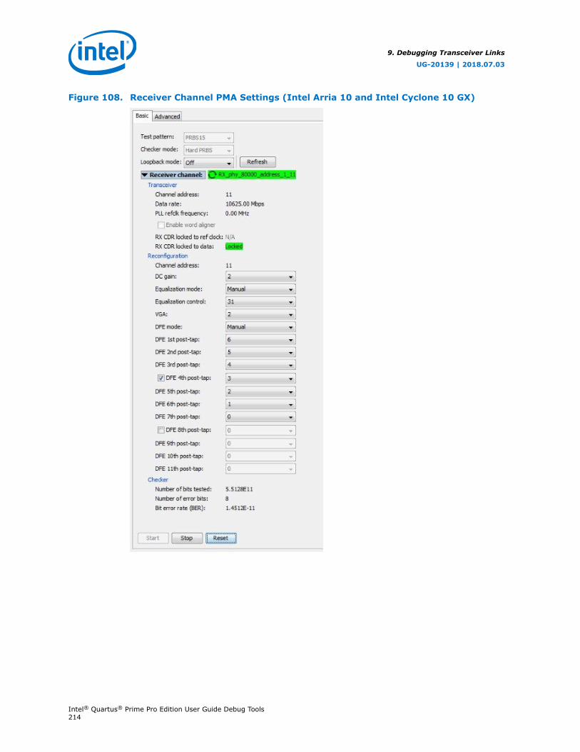
Figure 108. Receiver Channel PMA Settings (Intel Arria 10 and Intel Cyclone 10 GX)
9. Debugging Transceiver Links
UG-20139 | 2018.07.03
Intel® Quartus® Prime Pro Edition User Guide Debug Tools214
Figure 109. Transceiver Link PMA Settings (Intel Arria 10 and Intel Cyclone 10 GX)
Related Information
• Instantiating and Parameterizing Debug IP cores on page 203
• PMA ParametersIn Intel Arria 10 Transceiver PHY User Guide
• PMA ParametersIn Intel Cyclone 10 GX Transceiver PHY User Guide
9. Debugging Transceiver Links
UG-20139 | 2018.07.03
Intel® Quartus® Prime Pro Edition User Guide Debug Tools215
9.11.2. Intel Stratix 10 L- and H-Tile PMA Settings
The following figures show the PMA settings for Intel Stratix 10 L- and H-Tile devices.
Figure 110. Transmitter Channel PMA Settings (Intel Stratix 10 L- and H-Tile)
9. Debugging Transceiver Links
UG-20139 | 2018.07.03
Intel® Quartus® Prime Pro Edition User Guide Debug Tools216
Figure 111. Receiver Channel PMA Settings (Intel Stratix 10 L- and H-Tile)
9. Debugging Transceiver Links
UG-20139 | 2018.07.03
Intel® Quartus® Prime Pro Edition User Guide Debug Tools217
Figure 112. Transceiver Link PMA Settings (Intel Stratix 10 L- and H-Tile)
Related Information
• Instantiating and Parameterizing Debug IP cores
• Analog PMA Settings ParametersIn Intel Stratix 10 L- and H-Tile Transceiver PHY User Guide
9.11.3. Intel Stratix 10 E-Tile PMA Settings
The following figures show the PMA settings for Intel Stratix 10 E-Tile devices.
9. Debugging Transceiver Links
UG-20139 | 2018.07.03
Intel® Quartus® Prime Pro Edition User Guide Debug Tools218

Figure 113. Intel Stratix 10 E-Tile Transmitter Channel PMA SettingsThe Transceiver Toolkit does not support Rules Based Configuration validity checking in Intel Stratix 10 E-Tiledevices. Correct parameter combinations can appear in red. To determine validity of the transmitter setting,refer to the Intel Stratix 10 E-Tile Transceiver PHY User Guide.
9. Debugging Transceiver Links
UG-20139 | 2018.07.03
Intel® Quartus® Prime Pro Edition User Guide Debug Tools219
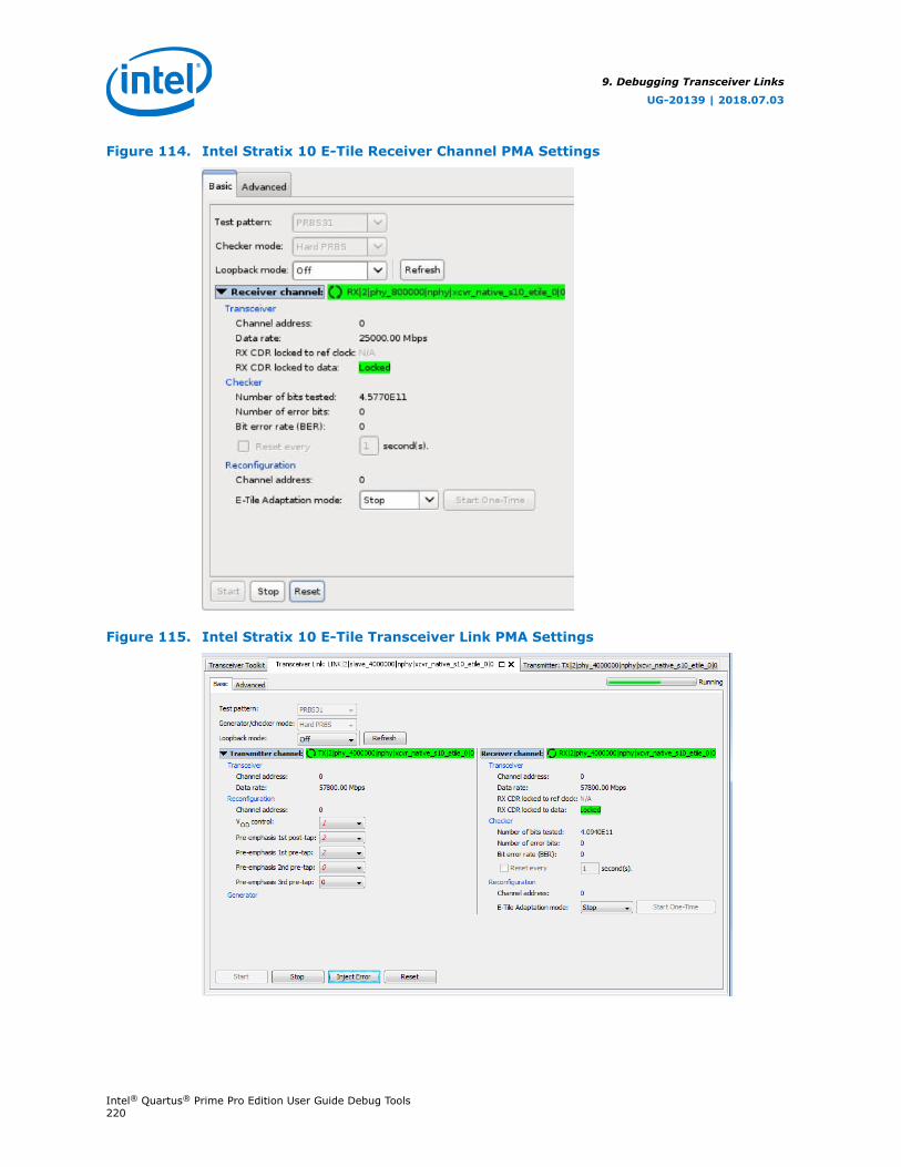
Figure 114. Intel Stratix 10 E-Tile Receiver Channel PMA Settings
Figure 115. Intel Stratix 10 E-Tile Transceiver Link PMA Settings
9. Debugging Transceiver Links
UG-20139 | 2018.07.03
Intel® Quartus® Prime Pro Edition User Guide Debug Tools220
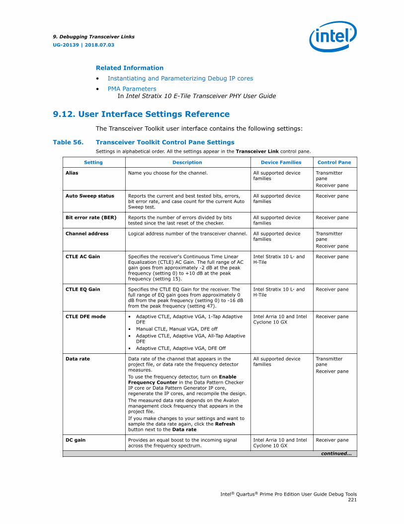
Related Information
• Instantiating and Parameterizing Debug IP cores
• PMA ParametersIn Intel Stratix 10 E-Tile Transceiver PHY User Guide
9.12. User Interface Settings Reference
The Transceiver Toolkit user interface contains the following settings:
Table 56. Transceiver Toolkit Control Pane SettingsSettings in alphabetical order. All the settings appear in the Transceiver Link control pane.
Setting Description Device Families Control Pane
Alias Name you choose for the channel. All supported devicefamilies
TransmitterpaneReceiver pane
Auto Sweep status Reports the current and best tested bits, errors,bit error rate, and case count for the current AutoSweep test.
All supported devicefamilies
Receiver pane
Bit error rate (BER) Reports the number of errors divided by bitstested since the last reset of the checker.
All supported devicefamilies
Receiver pane
Channel address Logical address number of the transceiver channel. All supported devicefamilies
TransmitterpaneReceiver pane
CTLE AC Gain Specifies the receiver's Continuous Time LinearEqualization (CTLE) AC Gain. The full range of ACgain goes from approximately -2 dB at the peakfrequency (setting 0) to +10 dB at the peakfrequency (setting 15).
Intel Stratix 10 L- andH-Tile
Receiver pane
CTLE EQ Gain Specifies the CTLE EQ Gain for the receiver. Thefull range of EQ gain goes from approximately 0dB from the peak frequency (setting 0) to -16 dBfrom the peak frequency (setting 47).
Intel Stratix 10 L- andH-Tile
Receiver pane
CTLE DFE mode • Adaptive CTLE, Adaptive VGA, 1-Tap AdaptiveDFE
• Manual CTLE, Manual VGA, DFE off• Adaptive CTLE, Adaptive VGA, All-Tap Adaptive
DFE• Adaptive CTLE, Adaptive VGA, DFE Off
Intel Arria 10 and IntelCyclone 10 GX
Receiver pane
Data rate Data rate of the channel that appears in theproject file, or data rate the frequency detectormeasures.To use the frequency detector, turn on EnableFrequency Counter in the Data Pattern CheckerIP core or Data Pattern Generator IP core,regenerate the IP cores, and recompile the design.The measured data rate depends on the Avalonmanagement clock frequency that appears in theproject file.If you make changes to your settings and want tosample the data rate again, click the Refreshbutton next to the Data rate
All supported devicefamilies
TransmitterpaneReceiver pane
DC gain Provides an equal boost to the incoming signalacross the frequency spectrum.
Intel Arria 10 and IntelCyclone 10 GX
Receiver pane
continued...
9. Debugging Transceiver Links
UG-20139 | 2018.07.03
Intel® Quartus® Prime Pro Edition User Guide Debug Tools221
Setting Description Device Families Control Pane
DFE mode Decision feedback equalization (DFE) for improvingsignal quality.
Device Value
Intel Arria 10 and IntelCyclone 10 GX
1-11
In Intel Arria 10 devices, DFE modes are Off,Manual and Adaptation Enabled. DFE inAdaptation Enabled mode automatically tries tofind the best tap values.
Intel Arria 10 and IntelCyclone 10 GX
Receiver pane
E-Tile AdaptationMode
Specifies the tuning mode for the Receiverequalizer parameters:• Continuous Adaptation• One-Time AdaptationNote: When running the One-Time Adaptation
Mode, ensure that BER measurement isnot running at the same time.
The Start One-Time button remains pressed untilthe adaptation finishes.
Intel Stratix 10 E-Tile Receiver pane
Equalization control Boosts the high-frequency gain of the incomingsignal to compensate for the low-pass filter effectsof the physical medium. When you use this optionwith DFE, use DFE in Manual or AdaptationEnabled mode.
Intel Arria 10 and IntelCyclone 10 GX
Receiver pane
Equalization mode For Intel Arria 10 devices, you can setEqualization Mode to Manual or Triggered.
Intel Arria 10 and IntelCyclone 10 GX
Receiver pane
Error rate limit Turns on or off error rate limits. Start checkingafter specifies the number of bits the toolkit waitsbefore looking at the bit error rate (BER) for thenext two checks.Bit error rate achieves below sets upper biterror rate limits. If the error rate is better than theset error rate, the test ends.Bit error rate exceeds sets lower bit error ratelimits. If the error rate is worse than the set errorrate, the test ends.
All supported devicefamilies
Receiver pane
Generator/Checkermode
Specifies Data pattern checker or Serial bitcomparator for BER tests.If you enable Serial bit comparator the DataPattern Generator sends the PRBS pattern, but theserial bit comparator checks the pattern.In Bypass mode, clicking Start begins countingon the Serial bit comparator.For BER testing:• Intel Arria 10 devices support the Data Pattern
Checker and the Hard PRBS.
All supported devicefamilies
TransmitterpaneReceiver pane
Increase test range For the selected set of controls, increases the spanof tests by one unit down for the minimum, andone unit up for the maximum.You can span either PMA Analog controls (non-DFEcontrols), or the DFE controls. You can quickly setup a test to check if any PMA setting combinationsnear your current best yields better results.To use, right-click the Advanced panel
All supported devicefamilies
Receiver pane
continued...
9. Debugging Transceiver Links
UG-20139 | 2018.07.03
Intel® Quartus® Prime Pro Edition User Guide Debug Tools222
Setting Description Device Families Control Pane
Maximum tested bits Sets the maximum number of bits tested for eachtest iteration.
All supported devicefamilies
Receiver pane
Number of bits tested Specifies the number of bits tested since the lastreset of the checker.
All supported devicefamilies
Receiver pane
Number of error bits Specifies the number of error bits encounteredsince the last reset of the checker.
All supported devicefamilies
Receiver pane
PLL refclk freq Channel reference clock frequency that appears inthe project file, or reference clock frequencycalculated from the measured data rate.
All supported devicefamilies
TransmitterpaneReceiver pane
Populate with Right-click the Advanced panel to load currentvalues on the device as a starting point, or initiallyload the best settings auto sweep determines. TheIntel Quartus Prime software automatically appliesthe values you specify in the drop-down lists forthe Transmitter settings and Receiver settings.
All supported devicefamilies
Receiver pane
Preamble word Word to send out if you use the preamble mode(only if you use soft PRBS Data Pattern Generatorand Checker).
All supported devicefamilies
Transmitterpane
Pre-emphasis This programmable module boosts highfrequencies in the transmit data for each transmitbuffer signal. This action counteracts possibleattenuation in the transmission media.
All supported devicefamilies
Transmitterpane
Receiver channel Specifies the name of the selected receiverchannel.
All supported devicefamilies
Receiver pane
Refresh Button After loading the .pof file, loads fresh settingsfrom the registers after running dynamicreconfiguration.
All supported devicefamilies
TransmitterpaneReceiver pane
Reset Resets the current test. All supported devicefamilies
Receiver pane
Rules BasedConfiguration (RBC)validity checking
Displays in red any invalid combination of settingsfor each list under Transmitter settings andReceiver settings, based on previous settings.When you enable this option, the settings appearin red to indicate the current combination isinvalid. This action avoids manually testing invalidsettings that you cannot compile for your design,and prevents setting the device into an invalidmode for extended periods of time and potentiallydamaging the circuits.
Intel Arria 10Intel Cyclone 10 GXIntel Stratix 10 L- andH-Tile
Receiver pane
Run length Sets coverage parameters for test runs. All supported devicefamilies
TransmitterpaneReceiver pane
RX CDR PLL status Shows the receiver in lock-to-reference (LTR)mode. When in auto-mode, if data cannot belocked, this signal alternates in LTD mode if theCDR is locked to data.
All supported devicefamilies
Receiver pane
RX CDR data status Shows the receiver in lock-to-data (LTD) mode.When in auto-mode, if data cannot be locked, thesignal stays high when locked to data and neverswitches.
All supported devicefamilies
Receiver pane
Serial loopbackenabled
Inserts a serial loopback before the buffers,allowing you to form a link on a transmitter andreceiver pair on the same physical channel of thedevice.
All supported devicefamilies
TransmitterpaneReceiver pane
continued...
9. Debugging Transceiver Links
UG-20139 | 2018.07.03
Intel® Quartus® Prime Pro Edition User Guide Debug Tools223
Setting Description Device Families Control Pane
Start Starts the pattern generator or checker on thechannel to verify incoming data.
All supported devicefamilies
TransmitterpaneReceiver pane
Stop Stops generating patterns and testing the channel. All supported devicefamilies
TransmitterpaneReceiver pane
Test pattern Test pattern sent by the transmitter channel.
Device Family Test Patterns Available
Intel Arria 10and IntelCyclone 10 GX
PRBS9, PRBS15, PRBS23,and PRBS31.
Intel Stratix10 L- and H-Tile
PRBS7,PRBS9, PRBS15,PRBS23, and PRBS31
Intel Stratix10 E-Tile
• NRZ: PRBS7,PRBS9,PRBS11,PRBS13,PRBS15, PRBS23, and PRBS31.
• PAM4: PRBS7Q,PRBS9Q,PRBS11Q,PRBS13Q,PRBS15Q, PRBS23Q, andPRBS31Q.
All supported devicefamilies
TransmitterpaneReceiver pane
Time limit Specifies the time limit unit and value to have amaximum bounds time limit for each test iteration.
All supported devicefamilies
Receiver
Transmitter channel Specifies the name of the selected transmitterchannel.
All supported devicefamilies
Transmitterpane
TX/CMU PLL status Specifies whether the transmitter channel PLL islocked to the reference clock.
All supported devicefamilies
Transmitterpane
Use preamble uponstart
If turned on, sends the preamble word before thetest pattern. If turned off, starts sending the testpattern immediately.
All supported devicefamilies
Transmitterpane
VGA The variable gain amplifier (VGA) amplifies thesignal amplitude and ensures a constant voltageswing before the data enters the Clock DataRecovery (CDR) block for sampling. Thisassignment controls the VGA output voltage swing,and allows values from 0 to 7.
Intel Arria 10 and IntelCyclone 10 GX
Receiver pane
VGA DC gain Specifies the VGA Gain for the receiver. The fullrange of VGA gain goes from approximately -5 dB(setting 0) to +7 dB (setting 31).
Intel Stratix 10 L- andH-Tile
Receiver pane
VOD control Programmable transmitter differential outputvoltage.
All supported devicefamilies
Transmitterpane
Related Information
Channel Manager on page 197
9. Debugging Transceiver Links
UG-20139 | 2018.07.03
Intel® Quartus® Prime Pro Edition User Guide Debug Tools224
9.13. Troubleshooting Common Errors
Missing high-speed link pin connections
Check the pin connections to identify high-speed links (tx_p/n and rx_p/n) aremissing. When porting an older design to the latest version of the Intel Quartus Primesoftware, make sure that these connections exist after porting.
Reset Issues:
Ensure that the reset input to the Transceiver Native PHY, Transceiver Reset Controller,and ATX PLL Intel FPGA IPs is not held active (1'b1). The Transceiver Toolkithighlights in red all the Transceiver Native PHY channels that you are setting up.
Unconnected reconfig_clk
You must connect and drive the reconfig_clk input to the Transceiver Native PHYand ATX PLL Intel FPGA IPs. Otherwise, the toolkit does not display the transceiverlink channel.
9.14. Scripting API Reference
The Intel Quartus Prime software provides an API to access Transceiver Toolkitfunctions using Tcl commands, and script tasks such as linking device resources andidentifying high-speed serial links.
To save the project setup in a Tcl script for use in subsequent testing sessions:
1. Set up and define links that describe the entire physical system.
2. Click Save Tcl Script to save the setup for future use.
You can also build a custom test routine script.
To run the scripts, double-click the script name in the System Explorer scripts folder.
To view a list of the available Tcl command descriptions from the Tcl Console window,including example usage:
1. In the Tcl console, type help help. The Console displays all Transceiver ToolkitTcl commands.
2. Type help <command name>. The Console displays the command description.
9.14.1. Transceiver Toolkit Commands
The following tables list the available Transceiver Toolkit scripting commands.
9. Debugging Transceiver Links
UG-20139 | 2018.07.03
Intel® Quartus® Prime Pro Edition User Guide Debug Tools225

Table 57. Transceiver Toolkit channel_rx Commands
Command Arguments Function
transceiver_channel_rx_get_data <service-path> Returns a list of the currentchecker data. The results are inthe order of number of bits,number of errors, and bit errorrate.
transceiver_channel_rx_get_dcgain <service-path> Gets the DC gain value on thereceiver channel.
transceiver_channel_rx_get_dfe_tap_value <service-path> <tapposition>
Gets the current tap value of thechannel you specify at the tapposition you specify.
transceiver_channel_rx_get_eqctrl <service-path> Gets the equalization controlvalue on the receiver channel.
transceiver_channel_rx_get_pattern <service-path> Returns the current data checkerpattern by name.
transceiver_channel_rx_has_dfe <service-path> Reports whether the channel youspecify has the DFE featureavailable.
transceiver_channel_rx_is_checking <service-path> Returns non-zero if the checker isrunning.
transceiver_channel_rx_is_dfe_enabled <service-path> Reports whether the DFE featureis enabled on the channel youspecify.
transceiver_channel_rx_is_locked <service-path> Returns non-zero if the checker islocked onto the incoming data.
transceiver_channel_rx_reset_counters <service-path> Resets the bit and error countersinside the checker.
transceiver_channel_rx_reset <service-path> Resets the channel you specify.
transceiver_channel_rx_set_dcgain <service-path> <value> Sets the DC gain value on thereceiver channel.
transceiver_channel_rx_set_dfe_enabled <service-path> <disable(0)/enable(1)>
Enables or disables the DFEfeature on the channel youspecify.
transceiver_channel_rx_set_dfe_tap_value <service-path> <tapposition> <tap value>
Sets the current tap value of thechannel you specify at the tapposition you specify to the valueyou specify.
transceiver_channel_rx_set_dfe_adaptive <service-path> <adaptive-mode>
Sets DFE adaptation mode of thechannel you specify.
Value Description
0 off
1 adaptive
transceiver_channel_rx_set_eqctrl <service-path> <value> Sets the equalization controlvalue on the receiver channel.
transceiver_channel_rx_start_checking <service-path> Starts the checker.
transceiver_channel_rx_stop_checking <service-path> Stops the checker.
continued...
9. Debugging Transceiver Links
UG-20139 | 2018.07.03
Intel® Quartus® Prime Pro Edition User Guide Debug Tools226

Command Arguments Function
transceiver_channel_rx_set_pattern <service-path> <pattern-name>
Sets the expected pattern to theone specified by the patternname.
transceiver_channel_rx_set_word_aligner_enabled
<service-path> <disable(0)/enable(1)>
Enables or disables the wordaligner of the channel youspecify.
transceiver_channel_rx_is_word_aligner_enabled
<service-path> <disable(0)/enable(1)>
Reports whether the word alignerfeature is enabled on the channelyou specify.
transceiver_channel_rx_is_locked <service-path> Returns non-zero if the checker islocked onto the incoming signal.
transceiver_channel_rx_is_rx_locked_to_data
<service-path> Returns 1 if transceiver is in lockto data (LTD) mode. Otherwise 0.
transceiver_channel_rx_is_rx_locked_to_ref
<service-path> Returns 1 if transceiver is in lockto reference (LTR) mode.Otherwise 0.
Table 58. Transceiver Toolkit channel_tx Commands
Command Arguments Function
transceiver_channel_tx_disable_preamble <service-path> Disables the preamble mode atthe beginning of generation.
transceiver_channel_tx_enable_preamble <service-path> Enables the preamble mode atthe beginning of generation.
transceiver_channel_tx_get_number_of_preamble_beats
<service-path> Returns the number of beats tosend out the preamble word.
transceiver_channel_tx_get_pattern <service-path> Returns the pattern.
transceiver_channel_tx_get_preamble_word <service-path> Returns the preamble word.
transceiver_channel_tx_get_preemph_pretap1
<service-path> Gets the pre-emphasis first pre-tap value on the transmitterchannel.
transceiver_channel_tx_get_preemph_posttap1
<service-path> Gets the pre-emphasis first post-tap value on the transmitterchannel.
transceiver_channel_tx_get_preemph_posttap2
<service-path> Gets the pre-emphasis secondpost-tap value on the transmitterchannel.
transceiver_channel_tx_get_preemph_pretap2
<service-path> Gets the pre-emphasis secondpre-tap value on the transmitterchannel.
transceiver_channel_tx_get_vodctrl <service-path> Gets the VOD control value on thetransmitter channel.
transceiver_channel_tx_inject_error <service-path> Injects a 1-bit error into thegenerator's output.
transceiver_channel_tx_is_generating <service-path> Returns non-zero if the generatoris running.
transceiver_channel_tx_is_preamble_enabled
<service-path> Returns non-zero if preamblemode is enabled.
continued...
9. Debugging Transceiver Links
UG-20139 | 2018.07.03
Intel® Quartus® Prime Pro Edition User Guide Debug Tools227

Command Arguments Function
transceiver_channel_tx_set_number_of_preamble_beats
<service-path> <number-of-preamble-beats>
Sets the number of beats to sendout the preamble word.
transceiver_channel_tx_set_pattern <service-path> <pattern-name>
Sets the output pattern to theone specified by the patternname.
transceiver_channel_tx_set_preamble_word <service-path> <preamble-word>
Sets the preamble word to besent out.
transceiver_channel_tx_set_preemph_pretap1
<service-path> <value> Sets the pre-emphasis first pre-tap value on the transmitterchannel.
transceiver_channel_tx_set_preemph_posttap1
<service-path> <value> Sets the pre-emphasis first post-tap value on the transmitterchannel.
transceiver_channel_tx_set_preemph_posttap2
<service-path> <value> Sets the pre-emphasis secondpost-tap value on the transmitterchannel.
transceiver_channel_tx_set_preemph_pretap2
<service-path> <value> Sets the pre-emphasis secondpre-tap value on the transmitterchannel.
transceiver_channel_tx_set_vodctrl <service-path> <vodctrlvalue>
Sets the VOD control value on thetransmitter channel.
transceiver_channel_tx_start_generation <service-path> Starts the generator.
transceiver_channel_tx_stop_generation <service-path> Stops the generator.
Table 59. Transceiver Toolkit Transceiver Toolkit debug_link Commands
Command Arguments Function
transceiver_debug_link_get_pattern <service-path> Gets the pattern the link uses torun the test.
transceiver_debug_link_is_running <service-path> Returns non-zero if the test isrunning on the link.
transceiver_debug_link_set_pattern <service-path> <datapattern>
Sets the pattern the link uses torun the test.
transceiver_debug_link_start_running <service-path> Starts running a test with thecurrently selected test pattern.
transceiver_debug_link_stop_running <service-path> Stops running the test.
Table 60. Transceiver Toolkit reconfig_analog Commands
Command Arguments Function
transceiver_reconfig_analog_get_logical_channel_address
<service-path> Gets the transceiver logic channeladdress currently set.
transceiver_reconfig_analog_get_rx_dcgain
<service-path> Gets the DC gain value on thereceiver channel specified by thecurrent logic channel address.
transceiver_reconfig_analog_get_rx_eqctrl
<service-path> Gets the equalization control valueon the receiver channel specified bythe current logic channel address.
continued...
9. Debugging Transceiver Links
UG-20139 | 2018.07.03
Intel® Quartus® Prime Pro Edition User Guide Debug Tools228
Command Arguments Function
transceiver_reconfig_analog_get_tx_preemph_pretap1
<service-path> Gets the pre-emphasis first pre-tapvalue on the transmitter channelspecified by the current logicchannel address.
transceiver_reconfig_analog_get_tx_preemph_posttap1
<service-path> Gets the pre-emphasis first post-tap value on the transmitterchannel specified by the currentlogic channel address.
transceiver_reconfig_analog_get_tx_preemph_posttap2
<service-path> Gets the pre-emphasis secondpost-tap value on the transmitterchannel specified by the currentlogic channel address.
transceiver_reconfig_analog_get_tx_preemph_pretap2
<service-path> Gets the pre-emphasis second pre-tap value on the transmitterchannel specified by the currentlogic channel address.
transceiver_reconfig_analog_get_tx_vodctrl
<service-path> Gets the VOD control value on thetransmitter channel specified by thecurrent logic channel address.
transceiver_reconfig_analog_set_logical_channel_address
<service-path> <logic channeladdress>
Sets the transceiver logic channeladdress.
transceiver_reconfig_analog_set_rx_dcgain
<service-path> <dc_gainvalue>
Sets the DC gain value on thereceiver channel specified by thecurrent logic channel address
transceiver_reconfig_analog_set_rx_eqctrl
<service-path> <eqctrl value> Sets the equalization control valueon the receiver channel specified bythe current logic channel address.
transceiver_reconfig_analog_set_tx_preemph_pretap1
<service-path> <value> Sets the pre-emphasis first pre-tapvalue on the transmitter channelspecified by the current logicchannel address.
transceiver_reconfig_analog_set_tx_preemph_posttap1
<service-path> < value> Sets the pre-emphasis first post-tap value on the transmitterchannel specified by the currentlogic channel address.
transceiver_reconfig_analog_set_tx_preemph_posttap2
<service-path> <value> Sets the pre-emphasis second post-tap value on the transmitterchannel specified by the currentlogic channel address.
transceiver_reconfig_analog_set_tx_preemph_pretap2
<service-path> <value> Sets the pre-emphasis second pre-tap value on the transmitterchannel specified by the currentlogic channel address.
transceiver_reconfig_analog_set_tx_vodctrl
<service-path> <vodctrl value> Sets the VOD control value on thetransmitter channel specified by thecurrent logic channel address.
Table 61. Channel Type Commands
Command Arguments Function
get_channel_type <service-path> <logical-channel-num>
Reports the detected type (GX/GT) of channel <logical-channel-num> for the reconfiguration block located at <service-path>.
set_channel_type <service-path> <logical-channel-num> <channel-type>
Overrides the detected channel type of channel <logical-channel-num> for the reconfiguration block located at <service-path> to thetype specified (0:GX, 1:GT).
9. Debugging Transceiver Links
UG-20139 | 2018.07.03
Intel® Quartus® Prime Pro Edition User Guide Debug Tools229

9.14.2. Data Pattern Generator Commands
You can use Data Pattern Generator commands to control data patterns for debuggingtransceiver channels. You must instantiate the Data Pattern Generator component tosupport these commands.
Table 62. Soft Data Pattern Generator Commands
Command Arguments Function
data_pattern_generator_start <service-path> Starts the data pattern generator.
data_pattern_generator_stop <service-path> Stops the data pattern generator.
data_pattern_generator_is_generating <service-path> Returns non-zero if the generator isrunning.
data_pattern_generator_inject_error <service-path> Injects a 1-bit error into the generatoroutput.
data_pattern_generator_set_pattern <service-path><pattern-name>
Sets the output pattern that <pattern-name> specifies.
Value Description
• PRBS7• PRBS15• PRBS23• PRBS31
Pseudo-random binarysequences. PRBS filesare clear text, and youcan modify the PRBSfiles.
HF Outputs high frequency,constant pattern ofalternating 0s and 1s
LF Outputs low frequency,constant pattern of10b’1111100000 for 10-bit symbols and8b’11110000 for 8-bitsymbols
data_pattern_generator_get_pattern <service-path> Returns currently selected outputpattern.
data_pattern_generator_get_available_patterns <service-path> Returns a list of available data patternsby name.
data_pattern_generator_enable_preamble <service-path> Enables the preamble mode at thebeginning of generation.
data_pattern_generator_disable_preamble <service-path> Disables the preamble mode at thebeginning of generation.
data_pattern_generator_is_preamble_enabled <service-path> Returns a non-zero value if preamblemode is enabled.
data_pattern_generator_set_preamble_word <preamble-word>
Sets the preamble word (could be 32-bitor 40-bit).
data_pattern_generator_get_preamble_word <service-path> Gets the preamble word.
data_pattern_generator_set_preamble_beats <service-path><number-of-preamble-beats>
Sets the number of beats to send out inthe preamble word.
continued...
9. Debugging Transceiver Links
UG-20139 | 2018.07.03
Intel® Quartus® Prime Pro Edition User Guide Debug Tools230
Command Arguments Function
data_pattern_generator_get_preamble_beats <service-path> Returns the currently set number ofbeats to send out in the preamble word.
data_pattern_generator_fcnter_start <service-path><max-cycles>
Sets the max cycle count and starts thefrequency counter.
data_pattern_generator_check_status <service-path> Queries the data pattern generator forcurrent status. Returns a bitmapindicating the status, with bits definedas follows:
Value Description
0 Enabled
1 Bypass enabled
2 Avalon
3 Sink ready
4 Source valid
5 Frequency counter enabled
data_pattern_generator_fcnter_report <service-path><force-stop>
Reports the current measured clockratio, stopping the counting firstdepending on <force-stop>.
Table 63. Hard Data Pattern Generator Commands
Command Arguments Function
hard_prbs_generator_start <service-path> Starts the generator that you specify.
hard_prbs_generator_stop <service-path> Stops the generator that you specify.
hard_prbs_generator_is_generating <service-path> Checks the generation status. Returns:
Value Description
0 Generating
1 Otherwise
hard_prbs_generator_set_pattern <service-path><pattern>
Sets the pattern of the hard PRBS generatoryou specify to pattern.
hard_prbs_generator_get_pattern <service-path> Returns the current pattern for a given hardPRBS generator.
hard_prbs_generator_get_available_patterns <service-path> Returns the available patterns for a givenhard PRBS generator.
9.14.3. Data Pattern Checker Commands
You can use Data Pattern Checker commands to verify your generated data patterns.You must instantiate the Data Pattern Checker component to support thesecommands.
9. Debugging Transceiver Links
UG-20139 | 2018.07.03
Intel® Quartus® Prime Pro Edition User Guide Debug Tools231
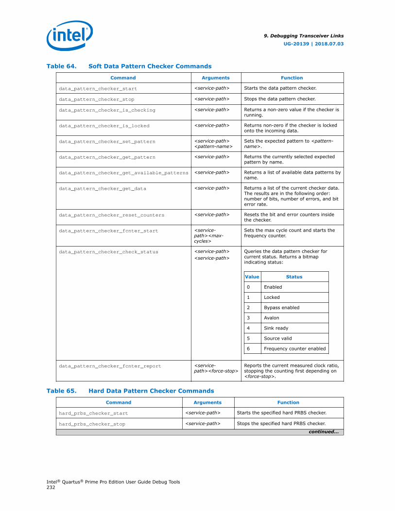
Table 64. Soft Data Pattern Checker Commands
Command Arguments Function
data_pattern_checker_start <service-path> Starts the data pattern checker.
data_pattern_checker_stop <service-path> Stops the data pattern checker.
data_pattern_checker_is_checking <service-path> Returns a non-zero value if the checker isrunning.
data_pattern_checker_is_locked <service-path> Returns non-zero if the checker is lockedonto the incoming data.
data_pattern_checker_set_pattern <service-path><pattern-name>
Sets the expected pattern to <pattern-name>.
data_pattern_checker_get_pattern <service-path> Returns the currently selected expectedpattern by name.
data_pattern_checker_get_available_patterns <service-path> Returns a list of available data patterns byname.
data_pattern_checker_get_data <service-path> Returns a list of the current checker data.The results are in the following order:number of bits, number of errors, and biterror rate.
data_pattern_checker_reset_counters <service-path> Resets the bit and error counters insidethe checker.
data_pattern_checker_fcnter_start <service-path><max-cycles>
Sets the max cycle count and starts thefrequency counter.
data_pattern_checker_check_status <service-path><service-path>
Queries the data pattern checker forcurrent status. Returns a bitmapindicating status:
Value Status
0 Enabled
1 Locked
2 Bypass enabled
3 Avalon
4 Sink ready
5 Source valid
6 Frequency counter enabled
data_pattern_checker_fcnter_report <service-path><force-stop>
Reports the current measured clock ratio,stopping the counting first depending on<force-stop>.
Table 65. Hard Data Pattern Checker Commands
Command Arguments Function
hard_prbs_checker_start <service-path> Starts the specified hard PRBS checker.
hard_prbs_checker_stop <service-path> Stops the specified hard PRBS checker.
continued...
9. Debugging Transceiver Links
UG-20139 | 2018.07.03
Intel® Quartus® Prime Pro Edition User Guide Debug Tools232

Command Arguments Function
hard_prbs_checker_is_checking <service-path> Checks the running status of the specifiedhard PRBS checker. Returns a non-zero valueif the checker is running.
hard_prbs_checker_set_pattern <service-path><pattern>
Sets the pattern of the specified hard PRBSchecker to parameter <pattern>.
hard_prbs_checker_get_pattern <service-path> Returns the current pattern for a given hardPRBS checker.
hard_prbs_checker_get_available_patterns <service-path> Returns the available patterns for a givenhard PRBS checker.
hard_prbs_checker_get_data <service-path> Returns the current bit and error count datafrom the specified hard PRBS checker.
hard_prbs_checker_reset_counters <service-path> Resets the bit and error counts of thespecified hard PRBS checker.
9.15. Debugging Transceiver Links Revision History
Document Version Intel QuartusPrime Version
Changes
2018.07.03 18.0.0 • Added topic: Device Support• Added support for Intel Stratix 10 TX/E-Tile.• Added Device Family column to table: Transceiver Toolkit Control Pane
Settings• Updated Figures for Intel Stratix 10 L- and H-Tile PMA Settings
2017.11.27 17.1.0 • Removed unsupported DFE adaptation mode from Transceiver Toolkitchannel_rx Commands table.
• Removed table: Transceiver Toolkit Decision Feedback Equalization(DFE) Commands.
• Removed table: Loopback Commands.
2017.11.06 17.1.0 • Added support for Intel Stratix 10 devices.• Renamed EyeQ to Eye Viewer.• Added section about running tests for Intel Stratix 10 H-Tile Production
devices using the Eye Viewer tool.• Updated topic "Transceiver Debugging Flow" and renamed to
"Transceiver Debugging Flow Walkthrough".• Removed deprecated topic about configuring a design example.• Updated instructions for instantiating and parameterizing Debug IP
cores.— Removed figure: "Altera Debug Master Endpoint Block Diagram".
• Added step on programming designs as a part of the debugging flow.• Updated information about debugging transceiver links for Intel Arria
10 devices.
2016.10.31 16.1.0 • Implemented Intel rebranding.• Removed EyeQ support for Intel Arria 10.• Renamed "Continuous Adaptation" to "Adaptation Enabled".
May 2015 15.0.0 • Added section about Implementation Differences Between Stratix V andArria 10.
• Added section about Recommended Flow for Arria 10 TransceiverToolkit Design with the Intel Quartus Prime Software.
• Added section about Transceiver Toolkit Troubleshooting
continued...
9. Debugging Transceiver Links
UG-20139 | 2018.07.03
Intel® Quartus® Prime Pro Edition User Guide Debug Tools233

Document Version Intel QuartusPrime Version
Changes
• Updated the following sections with information about using theTransceiver Toolkit with Arria 10 devices:— Serial Bit Comparator Mode— Arria 10 Support and Limitations— Configuring BER Tests— Configuring PRBS Signal Eye Tests— Adapting Altera Design Examples— Modifying Design Examples— Configuring Custom Traffic Signal Eye Tests— Configuring Link Optimization Tests— Configuring PMA Analog Setting Control— Running BER Tests— Toolkit GUI Setting Reference
• Reworked Table: Transceiver Toolkit IP Core Configuration• Replaced Figure: EyeQ Settings and Status Showing Results of Two Test
Runs with Figure: EyeQ Settings and Status Showing Results of ThreeTest Runs.
• Added Figure: Arria 10 Altera Debug Master Endpoint Block Diagram.• Added Figure: BER Test Configuration (Arria10/ Gen 10/ 20nm) Block
Diagram.• Added Figure: PRBS Signal Test Configuration (Arria 10/ 20nm) Block
Diagram.• Added Figure: Custom Traffic Signal Eye Test Configuration (Arria 10/
Gen 10/ 20nm) Block Diagram.• Added Figure: PMA Analog Setting Control Configuration (Arria 10/ Gen
10/ 20nm) Block Diagram.• Added Figure: One Channel Loopback Mode (Arria 10/ 20nm) Block
Diagram.• Added Figure: Four Channel Loopback Mode (Arria 10/ Gen 10/ 20nm)
Block Diagram.Software Version 15.0 Limitations• Transceiver Toolkit supports EyeQ for Arria 10 designs.• Supports optional hard acceleration for EyeQ. This allows for much
faster EyeQ data collection. Enable this in the Arria 10 TransceiverNative PHY IP core under the Dynamic Configuration tab. Turn onEnable ODI acceleration logic.
December, 2014 14.1.0 • Added section about Arria 10 support and limitations.
June, 2014 14.0.0 • Updated GUI changes for Channel Manager with popup menus, IPCatalog, Intel Quartus Prime, and Qsys.
• Added ADME and JTAG debug link info for Arria 10.• Added instructions to run Tcl script from command line.• Added heat map display option.• Added procedure to use internal PLL to generate reconfig_clk.• Added note stating RX CDR PLL status can toggle in LTD mode.
November, 2013 13.1.0 • Reorganization and conversion to DITA.
May, 2013 13.0.0 • Added Conduit Mode Support, Serial Bit Comparator, Required Files andTcl command tables.
November, 2012 12.1.0 • Minor editorial updates. Added Tcl help information and removed Tclcommand tables. Added 28-Gbps Transceiver support section.
August, 2012 12.0.1 • General reorganization and revised steps in modifying Altera exampledesigns.
June, 2012 12.0.0 • Maintenance release for update of Transceiver Toolkit features.
November, 2011 11.1.0 • Maintenance release for update of Transceiver Toolkit features.
continued...
9. Debugging Transceiver Links
UG-20139 | 2018.07.03
Intel® Quartus® Prime Pro Edition User Guide Debug Tools234

Document Version Intel QuartusPrime Version
Changes
May, 2011 11.0.0 • Added new Tcl scenario.
December, 2010 10.1.0 • Changed to new document template. Added new 10.1 release features.
August, 2010 10.0.1 • Corrected links.
July 2010 10.0.0 • Initial release.
Related Information
Documentation ArchiveFor previous versions of the Intel Quartus Prime Handbook, search thedocumentation archives.
9. Debugging Transceiver Links
UG-20139 | 2018.07.03
Intel® Quartus® Prime Pro Edition User Guide Debug Tools235

A. Intel Quartus Prime Pro Edition User GuidesRefer to the following user guides for comprehensive information on all phases of theIntel Quartus Prime Pro Edition FPGA design flow.
Related Information
• Getting Started User GuideIntroduces the basic features, files, and design flow of the Intel Quartus PrimePro Edition software, including managing Intel Quartus Prime Pro Editionprojects and IP, initial design planning considerations, and project migrationfrom previous software versions.
• Platform Designer User GuideDescribes creating and optimizing systems using Platform Designer, a systemintegration tool that simplifies integrating customized IP cores in your project.Platform Designer automatically generates interconnect logic to connectintellectual property (IP) functions and subsystems.
• Design Recommendations User GuideDescribes best design practices for designing FPGAs with the Intel QuartusPrime Pro Edition software. HDL coding styles and synchronous designpractices can significantly impact design performance. Following recommendedHDL coding styles ensures that Intel Quartus Prime Pro Edition synthesisoptimally implements your design in hardware.
• Compiler User GuideDescribes set up, running, and optimization for all stages of the Intel QuartusPrime Pro Edition Compiler. The Compiler synthesizes, places, and routes yourdesign before generating a device programming file.
• Design Optimization User GuideDescribes Intel Quartus Prime Pro Edition settings, tools, and techniques thatyou can use to achieve the highest design performance in Intel FPGAs.Techniques include optimizing the design netlist, addressing critical chains thatlimit retiming and timing closure, and optimization of device resource usage.
• Programmer User GuideDescribes operation of the Intel Quartus Prime Pro Edition Programmer, whichallows you to configure Intel FPGA devices, and program CPLD andconfiguration devices, via connection with an Intel FPGA download cable.
• Block-Based Design User GuideDescribes block-based design flows, also known as modular or hierarchicaldesign flows. These advanced flows enable preservation of design blocks (orlogic that comprises a hierarchical design instance) within a project, and reuseof design blocks in other projects.
UG-20139 | 2018.07.03
Intel Corporation. All rights reserved. Intel, the Intel logo, Altera, Arria, Cyclone, Enpirion, MAX, Nios, Quartusand Stratix words and logos are trademarks of Intel Corporation or its subsidiaries in the U.S. and/or othercountries. Intel warrants performance of its FPGA and semiconductor products to current specifications inaccordance with Intel's standard warranty, but reserves the right to make changes to any products and servicesat any time without notice. Intel assumes no responsibility or liability arising out of the application or use of anyinformation, product, or service described herein except as expressly agreed to in writing by Intel. Intelcustomers are advised to obtain the latest version of device specifications before relying on any publishedinformation and before placing orders for products or services.*Other names and brands may be claimed as the property of others.
ISO9001:2008Registered

• Partial Reconfiguration User GuideDescribes Partial Reconfiguration, an advanced design flow that allows you toreconfigure a portion of the FPGA dynamically, while the remaining FPGAdesign continues to function. Define multiple personas for a particular designregion, without impacting operation in other areas.
• Third-party Simulation User GuideDescribes RTL- and gate-level design simulation support for third-partysimulation tools by Aldec*, Cadence*, Mentor Graphics*, and Synopsys* thatallow you to verify design behavior before device programming. Includessimulator support, simulation flows, and simulating Intel FPGA IP.
• Third-party Synthesis User GuideDescribes support for optional synthesis of your design in third-party synthesistools by Mentor Graphics*, and Synopsys*. Includes design flow steps,generated file descriptions, and synthesis guidelines.
• Debug Tools User GuideDescribes a portfolio of Intel Quartus Prime Pro Edition in-system designdebugging tools for real-time verification of your design. These tools providevisibility by routing (or “tapping”) signals in your design to debugging logic.These tools include System Console, Signal Tap logic analyzer, TransceiverToolkit, In-System Memory Content Editor, and In-System Sources and ProbesEditor.
• Timing Analyzer User GuideExplains basic static timing analysis principals and use of the Intel QuartusPrime Pro Edition Timing Analyzer, a powerful ASIC-style timing analysis toolthat validates the timing performance of all logic in your design using anindustry-standard constraint, analysis, and reporting methodology.
• Power Analysis and Optimization User GuideDescribes the Intel Quartus Prime Pro Edition Power Analysis tools that allowaccurate estimation of device power consumption. Estimate the powerconsumption of a device to develop power budgets and design power supplies,voltage regulators, heat sink, and cooling systems.
• Design Constraints User GuideDescribes timing and logic constraints that influence how the Compilerimplements your design, such as pin assignments, device options, logicoptions, and timing constraints. Use the Interface Planner to prototypeinterface implementations, plan clocks, and quickly define a legal devicefloorplan. Use the Pin Planner to visualize, modify, and validate all I/Oassignments in a graphical representation of the target device.
• PCB Design Tools User GuideDescribes support for optional third-party PCB design tools by MentorGraphics* and Cadence*. Also includes information about signal integrityanalysis and simulations with HSPICE and IBIS Models.
• Scripting User GuideDescribes use of Tcl and command line scripts to control the Intel QuartusPrime Pro Edition software and to perform a wide range of functions, such asmanaging projects, specifying constraints, running compilation or timinganalysis, or generating reports.
A. Intel Quartus Prime Pro Edition User Guides
UG-20139 | 2018.07.03
Intel® Quartus® Prime Pro Edition User Guide Debug Tools237