Embed Size (px)
Citation preview
The information in this document is subject to change without notice. Before using this document, pleaseconfirm that this is the latest version.Not all products and/or types are available in every country. Please check with an NEC Electronics sales representative for availability and additional information.
MOS INTEGRATED CIRCUIT
μPD43256B256K-BIT CMOS STATIC RAM
32K-WORD BY 8-BIT
DATA SHEET
Document No. M10770EJFV0DS00 (15th edition) Date Published November 2008 Printed in Japan 1990, 1993, 1994
Description
The μPD43256B is a high speed, low power, and 262,144 bits (32,768 words by 8 bits) CMOS static RAM.
Battery backup is available. And A and B versions are wide voltage operations.
The μPD43256B is packed in 28-pin PLASTIC DIP, 28-pin PLASTIC SOP and 28-pin PLASTIC TSOP (I) (8 x 13.4 mm).
Features
• 32,768 words by 8 bits organization
• Fast access time: 70, 85, 100, 120 ns (MAX.)
• Low voltage operation (A version: VCC = 3.0 to 5.5 V, B version: VCC = 2.7 to 5.5 V)
• Low VCC data retention: 2.0 V (MIN.)
• /OE input for easy application
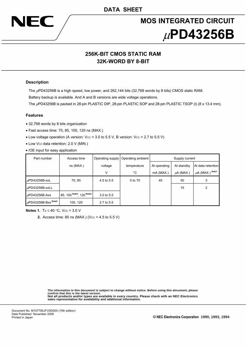
Part number Access time Operating supply Operating ambient Supply current
ns (MAX.) voltage temperature At operating At standby At data retention
V °C mA (MAX.) μA (MAX.) μA (MAX.) Note1
μPD43256B-xxL 70, 85 4.5 to 5.5 0 to 70 45 50 3
μPD43256B-xxLL 15 2
μPD43256B-Axx 85, 100 Note2, 120 Note2 3.0 to 5.5
μPD43256B-Bxx Note2 100, 120 2.7 to 5.5
Notes 1. TA ≤ 40 °C, VCC = 3.0 V
2. Access time: 85 ns (MAX.) (VCC = 4.5 to 5.5 V)
2
μPD43256B
Data Sheet M10770EJFV0DS
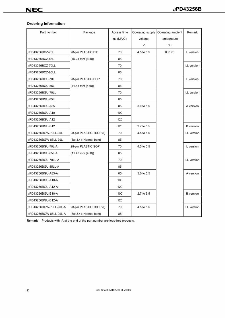
Ordering Information
Part number Package Access time Operating supply Operating ambient Remark
ns (MAX.) voltage temperature
V °C
μPD43256BCZ-70L 28-pin PLASTIC DIP 70 4.5 to 5.5 0 to 70 L version
μPD43256BCZ-85L (15.24 mm (600)) 85
μPD43256BCZ-70LL 70 LL version
μPD43256BCZ-85LL 85
μPD43256BGU-70L 28-pin PLASTIC SOP 70 L version
μPD43256BGU-85L (11.43 mm (450)) 85
μPD43256BGU-70LL 70 LL version
μPD43256BGU-85LL 85
μPD43256BGU-A85 85 3.0 to 5.5 A version
μPD43256BGU-A10 100
μPD43256BGU-A12 120
μPD43256BGU-B12 120 2.7 to 5.5 B version
μPD43256BGW-70LL-9JL 28-pin PLASTIC TSOP (I) 70 4.5 to 5.5 LL version
μPD43256BGW-85LL-9JL (8x13.4) (Normal bent) 85
μPD43256BGU-70L-A 28-pin PLASTIC SOP 70 4.5 to 5.5 L version
μPD43256BGU-85L-A (11.43 mm (450)) 85
μPD43256BGU-70LL-A 70 LL version
μPD43256BGU-85LL-A 85
μPD43256BGU-A85-A 85 3.0 to 5.5 A version
μPD43256BGU-A10-A 100
μPD43256BGU-A12-A 120
μPD43256BGU-B10-A 100 2.7 to 5.5 B version
μPD43256BGU-B12-A 120
μPD43256BGW-70LL-9JL-A 28-pin PLASTIC TSOP (I) 70 4.5 to 5.5 LL version
μPD43256BGW-85LL-9JL-A (8x13.4) (Normal bent) 85
Remark Products with -A at the end of the part number are lead-free products.
3
μPD43256B
Data Sheet M10770EJFV0DS
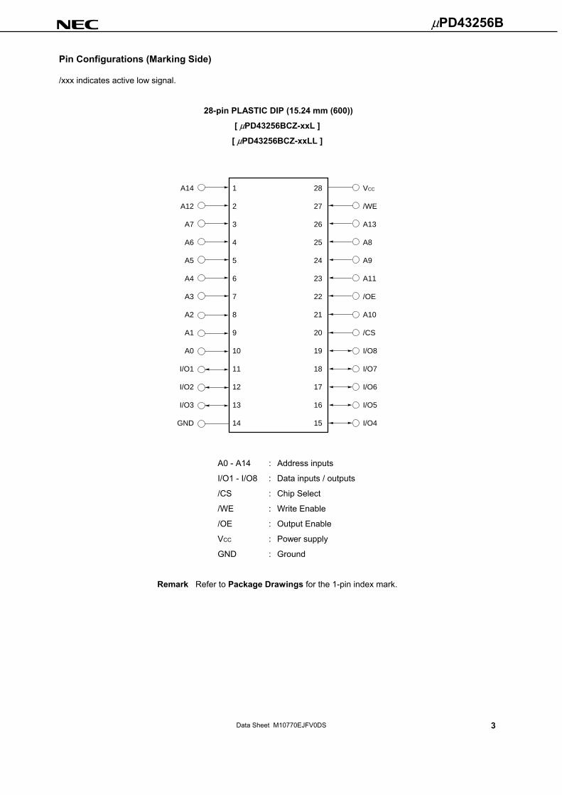
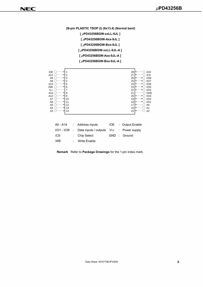
Pin Configurations (Marking Side)
/xxx indicates active low signal.
28-pin PLASTIC DIP (15.24 mm (600))
[ μPD43256BCZ-xxL ]
[ μPD43256BCZ-xxLL ]
A14
A12
A7
A6
A5
A4
A3
A2
A1
A0
I/O1
I/O2
I/O3
GND
VCC
/WE
A13
A8
A9
A11
/OE
A10
/CS
I/O8
I/O7
I/O6
I/O5
I/O4
1
2
3
4
5
6
7
8
9
10
11
12
13
14
28
27
26
25
24
23
22
21
20
19
18
17
16
15
A0 - A14 : Address inputs
I/O1 - I/O8 : Data inputs / outputs
/CS : Chip Select
/WE : Write Enable
/OE : Output Enable
VCC : Power supply
GND : Ground
Remark Refer to Package Drawings for the 1-pin index mark.
4
μPD43256B
Data Sheet M10770EJFV0DS
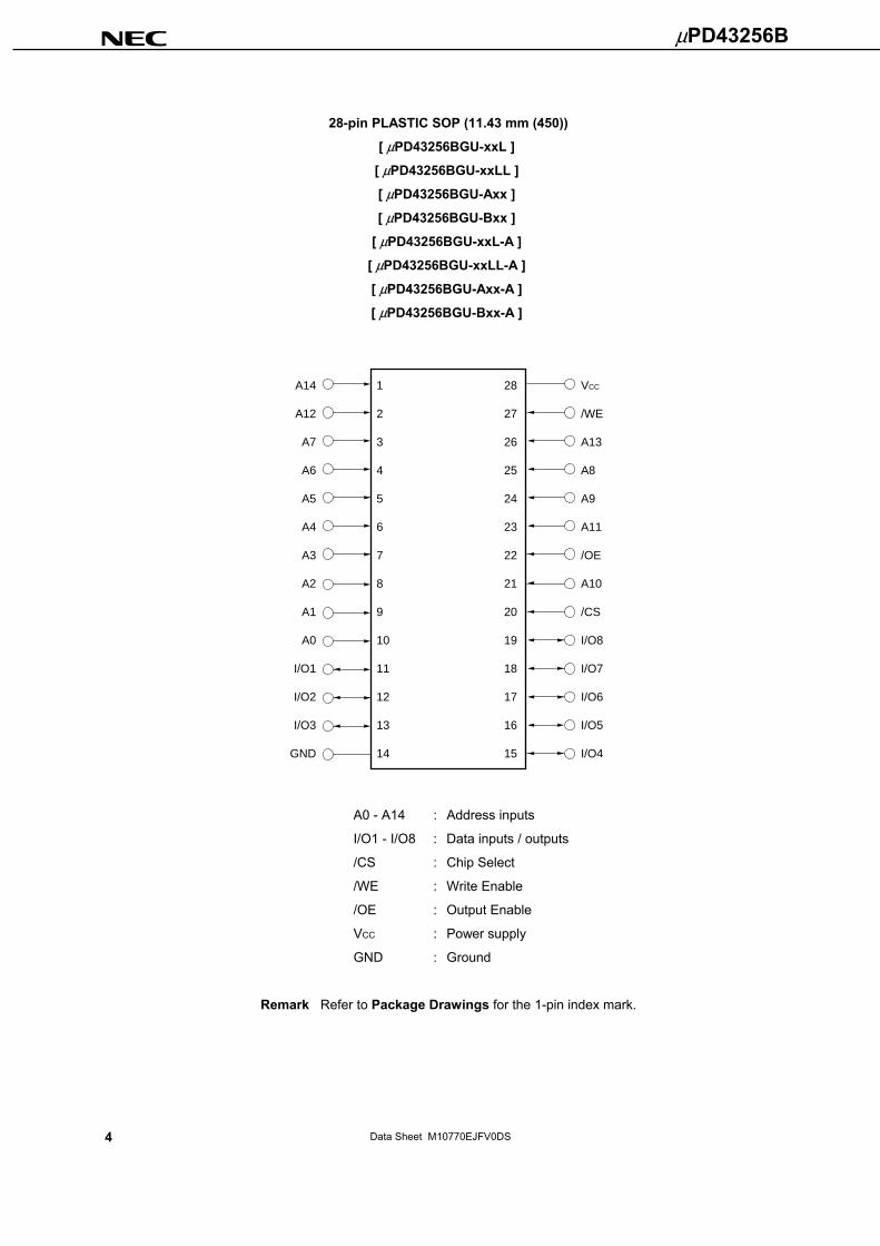
28-pin PLASTIC SOP (11.43 mm (450))
[ μPD43256BGU-xxL ]
[ μPD43256BGU-xxLL ]
[ μPD43256BGU-Axx ]
[ μPD43256BGU-Bxx ]
[ μPD43256BGU-xxL-A ]
[ μPD43256BGU-xxLL-A ]
[ μPD43256BGU-Axx-A ]
[ μPD43256BGU-Bxx-A ]
A14
A12
A7
A6
A5
A4
A3
A2
A1
A0
I/O1
I/O2
I/O3
GND
VCC
/WE
A13
A8
A9
A11
/OE
A10
/CS
I/O8
I/O7
I/O6
I/O5
I/O4
1
2
3
4
5
6
7
8
9
10
11
12
13
14
28
27
26
25
24
23
22
21
20
19
18
17
16
15
A0 - A14 : Address inputs
I/O1 - I/O8 : Data inputs / outputs
/CS : Chip Select
/WE : Write Enable
/OE : Output Enable
VCC : Power supply
GND : Ground
Remark Refer to Package Drawings for the 1-pin index mark.
5
μPD43256B
Data Sheet M10770EJFV0DS
28-pin PLASTIC TSOP (I) (8x13.4) (Normal bent)
[ μPD43256BGW-xxLL-9JL ]
[ μPD43256BGW-Axx-9JL ]
[ μPD43256BGW-Bxx-9JL ]
[ μPD43256BGW-xxLL-9JL-A ]
[ μPD43256BGW-Axx-9JL-A ]
[ μPD43256BGW-Bxx-9JL-A ]
/OEA11
A9A8
A13/WEVCC
A14A12
A7A6A5A4A3
A10/CSI/O8I/O7I/O6I/O5I/O4GNDI/O3I/O2I/O1A0A1A2
1234567891011121314
2827262524232221201918171615
A0 - A14 : Address inputs /OE : Output Enable
I/O1 - I/O8 : Data inputs / outputs VCC : Power supply
/CS : Chip Select GND : Ground
/WE : Write Enable
Remark Refer to Package Drawings for the 1-pin index mark.
6
μPD43256B
Data Sheet M10770EJFV0DS
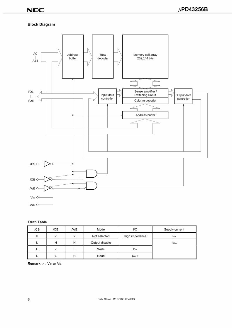
Block Diagram
Address buffer
Memory cell array262,144 bits
Input datacontroller
A0
A14
I/O8
Sense amplifier /Switching circuit
Column decoder
/WE
I/O1
VCC
GND
/CS
/OE
Addressbuffer
Rowdecoder
Output datacontroller
Truth Table
/CS /OE /WE Mode I/O Supply current
H × × Not selected High impedance ISB
L H H Output disable ICCA
L × L Write DIN
L L H Read DOUT
Remark × : VIH or VIL
7
μPD43256B
Data Sheet M10770EJFV0DS
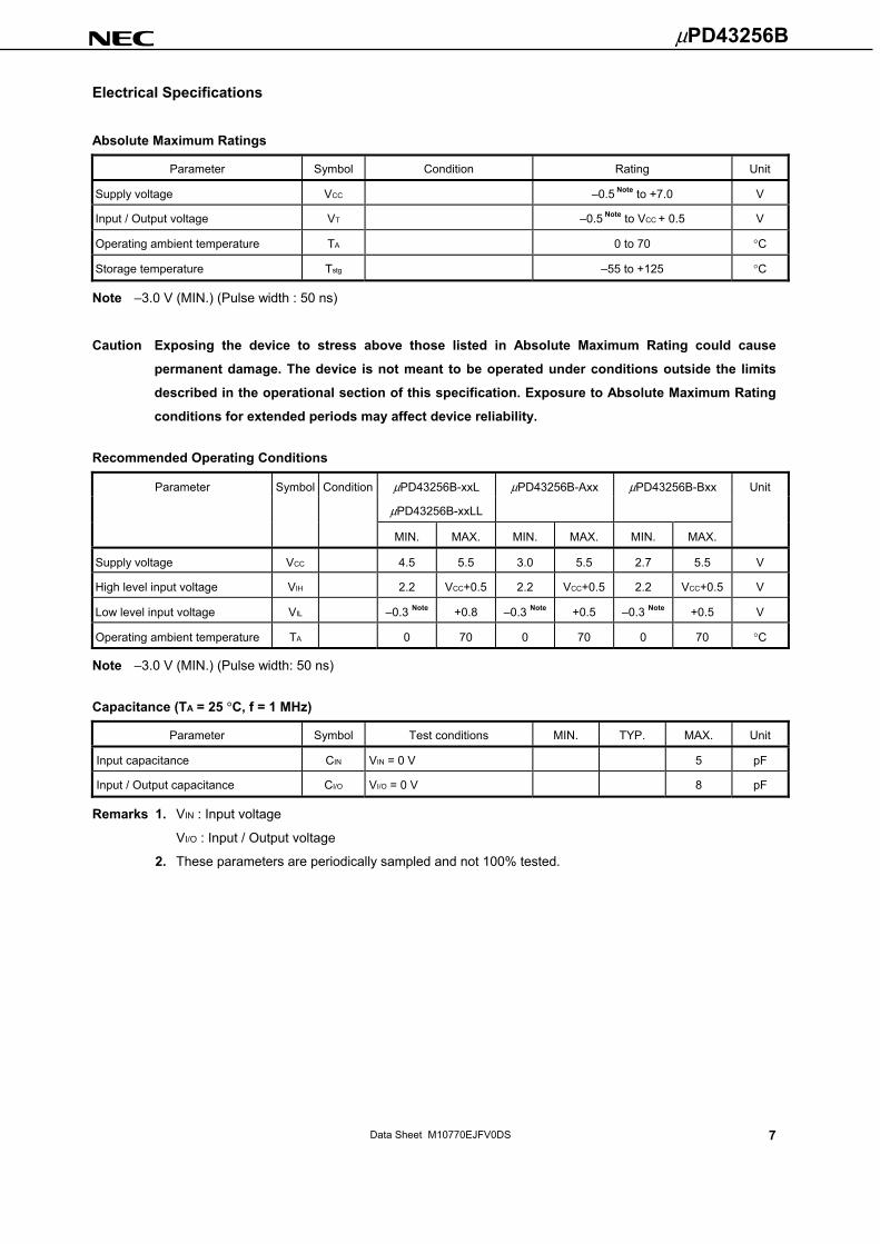
Electrical Specifications
Absolute Maximum Ratings
Parameter Symbol Condition Rating Unit
Supply voltage VCC –0.5 Note to +7.0 V
Input / Output voltage VT –0.5 Note to VCC + 0.5 V
Operating ambient temperature TA 0 to 70 °C
Storage temperature Tstg –55 to +125 °C
Note –3.0 V (MIN.) (Pulse width : 50 ns)
Caution Exposing the device to stress above those listed in Absolute Maximum Rating could cause
permanent damage. The device is not meant to be operated under conditions outside the limits
described in the operational section of this specification. Exposure to Absolute Maximum Rating
conditions for extended periods may affect device reliability.
Recommended Operating Conditions
Parameter Symbol Condition μPD43256B-xxL μPD43256B-Axx μPD43256B-Bxx Unit
μPD43256B-xxLL
MIN. MAX. MIN. MAX. MIN. MAX.
Supply voltage VCC 4.5 5.5 3.0 5.5 2.7 5.5 V
High level input voltage VIH 2.2 VCC+0.5 2.2 VCC+0.5 2.2 VCC+0.5 V
Low level input voltage VIL –0.3 Note +0.8 –0.3 Note +0.5 –0.3 Note +0.5 V
Operating ambient temperature TA 0 70 0 70 0 70 °C
Note –3.0 V (MIN.) (Pulse width: 50 ns)
Capacitance (TA = 25 °C, f = 1 MHz)
Parameter Symbol Test conditions MIN. TYP. MAX. Unit
Input capacitance CIN VIN = 0 V 5 pF
Input / Output capacitance CI/O VI/O = 0 V 8 pF
Remarks 1. VIN : Input voltage
VI/O : Input / Output voltage
2. These parameters are periodically sampled and not 100% tested.
8
μPD43256B
Data Sheet M10770EJFV0DS
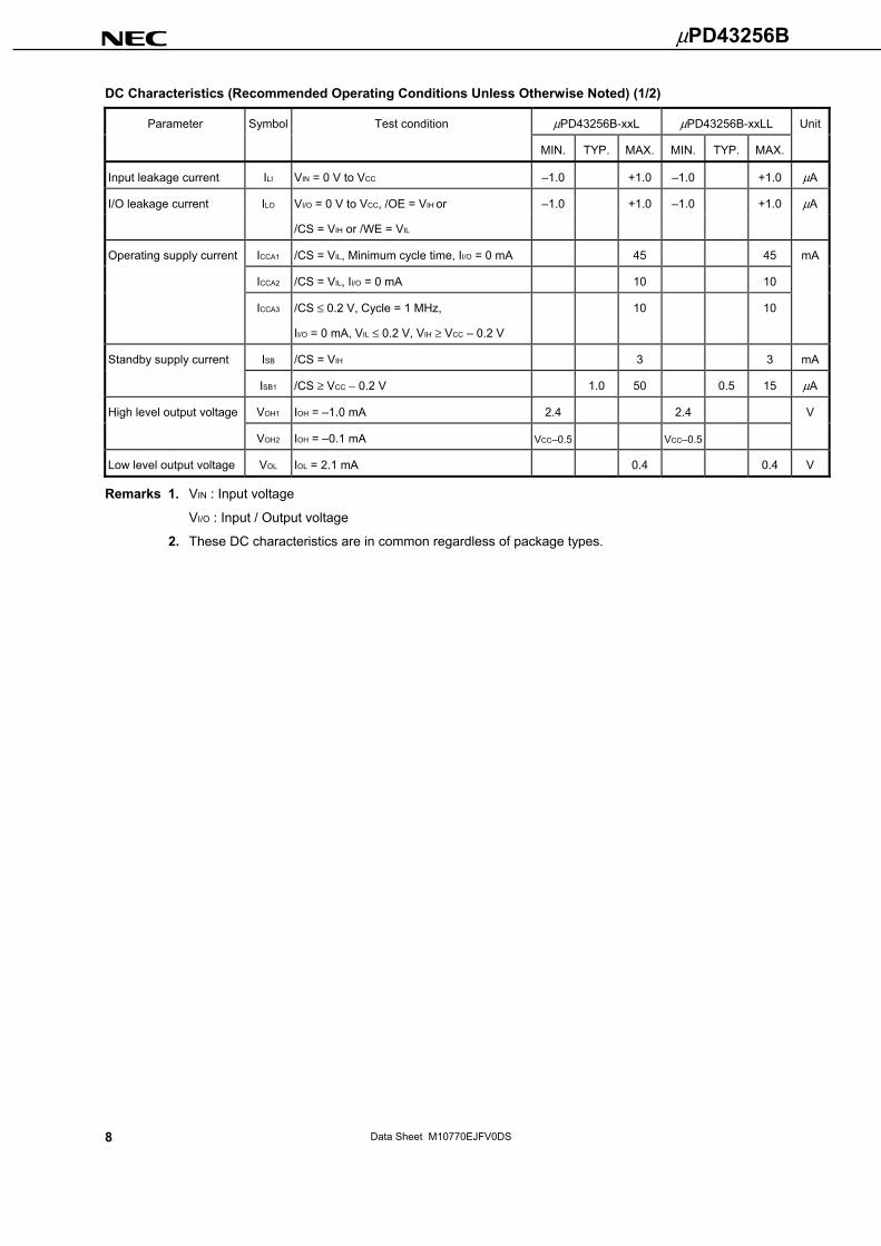
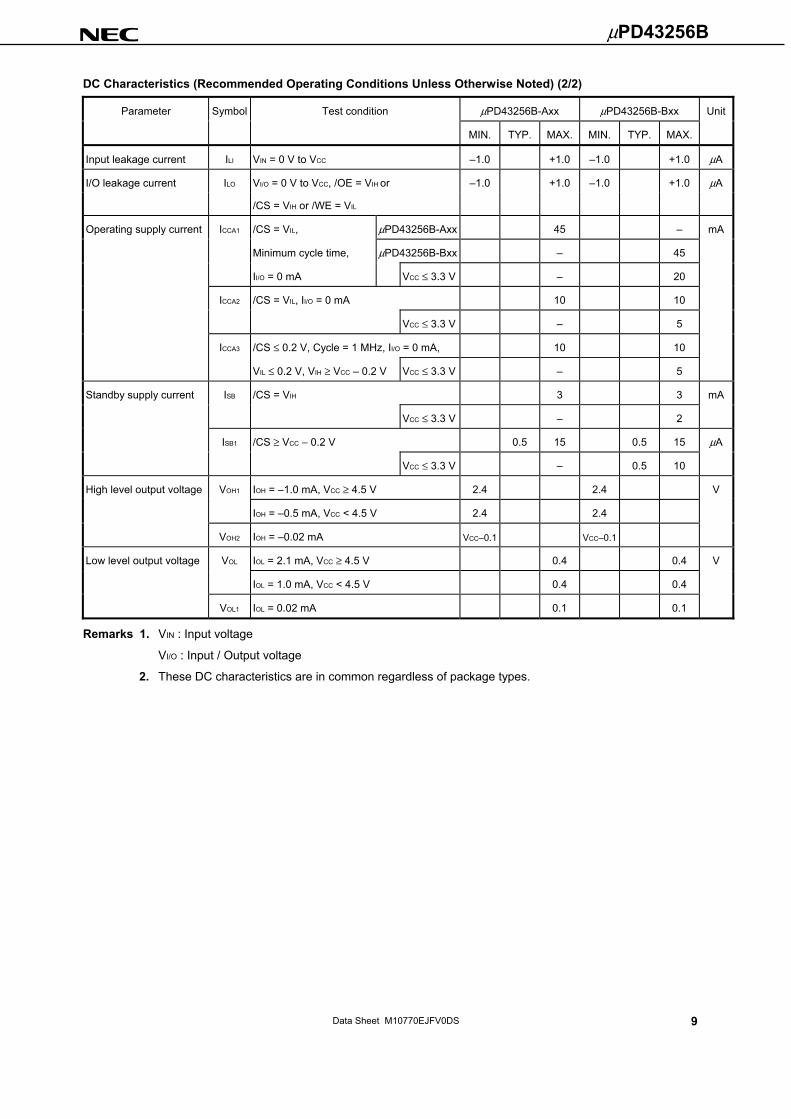
DC Characteristics (Recommended Operating Conditions Unless Otherwise Noted) (1/2)
Parameter Symbol Test condition μPD43256B-xxL μPD43256B-xxLL Unit
MIN. TYP. MAX. MIN. TYP. MAX.
Input leakage current ILI VIN = 0 V to VCC –1.0 +1.0 –1.0 +1.0 μA
I/O leakage current ILO VI/O = 0 V to VCC, /OE = VIH or –1.0 +1.0 –1.0 +1.0 μA
/CS = VIH or /WE = VIL
Operating supply current ICCA1 /CS = VIL, Minimum cycle time, II/O = 0 mA 45 45 mA
ICCA2 /CS = VIL, II/O = 0 mA 10 10
ICCA3 /CS ≤ 0.2 V, Cycle = 1 MHz, 10 10
II/O = 0 mA, VIL ≤ 0.2 V, VIH ≥ VCC – 0.2 V
Standby supply current ISB /CS = VIH 3 3 mA
ISB1 /CS ≥ VCC − 0.2 V 1.0 50 0.5 15 μA
High level output voltage VOH1 IOH = –1.0 mA 2.4 2.4 V
VOH2 IOH = –0.1 mA VCC–0.5 VCC–0.5
Low level output voltage VOL IOL = 2.1 mA 0.4 0.4 V
Remarks 1. VIN : Input voltage
VI/O : Input / Output voltage
2. These DC characteristics are in common regardless of package types.
9
μPD43256B
Data Sheet M10770EJFV0DS
DC Characteristics (Recommended Operating Conditions Unless Otherwise Noted) (2/2)
Parameter Symbol Test condition μPD43256B-Axx μPD43256B-Bxx Unit
MIN. TYP. MAX. MIN. TYP. MAX.
Input leakage current ILI VIN = 0 V to VCC –1.0 +1.0 –1.0 +1.0 μA
I/O leakage current ILO VI/O = 0 V to VCC, /OE = VIH or –1.0 +1.0 –1.0 +1.0 μA
/CS = VIH or /WE = VIL
Operating supply current ICCA1 /CS = VIL, μPD43256B-Axx 45 – mA
Minimum cycle time, μPD43256B-Bxx – 45
II/O = 0 mA VCC ≤ 3.3 V – 20
ICCA2 /CS = VIL, II/O = 0 mA 10 10
VCC ≤ 3.3 V – 5
ICCA3 /CS ≤ 0.2 V, Cycle = 1 MHz, II/O = 0 mA, 10 10
VIL ≤ 0.2 V, VIH ≥ VCC – 0.2 V VCC ≤ 3.3 V – 5
Standby supply current ISB /CS = VIH 3 3 mA
VCC ≤ 3.3 V – 2
ISB1 /CS ≥ VCC − 0.2 V 0.5 15 0.5 15 μA
VCC ≤ 3.3 V – 0.5 10
High level output voltage VOH1 IOH = –1.0 mA, VCC ≥ 4.5 V 2.4 2.4 V
IOH = –0.5 mA, VCC < 4.5 V 2.4 2.4
VOH2 IOH = –0.02 mA VCC–0.1 VCC–0.1
Low level output voltage VOL IOL = 2.1 mA, VCC ≥ 4.5 V 0.4 0.4 V
IOL = 1.0 mA, VCC < 4.5 V 0.4 0.4
VOL1 IOL = 0.02 mA 0.1 0.1
Remarks 1. VIN : Input voltage
VI/O : Input / Output voltage
2. These DC characteristics are in common regardless of package types.
10
μPD43256B
Data Sheet M10770EJFV0DS
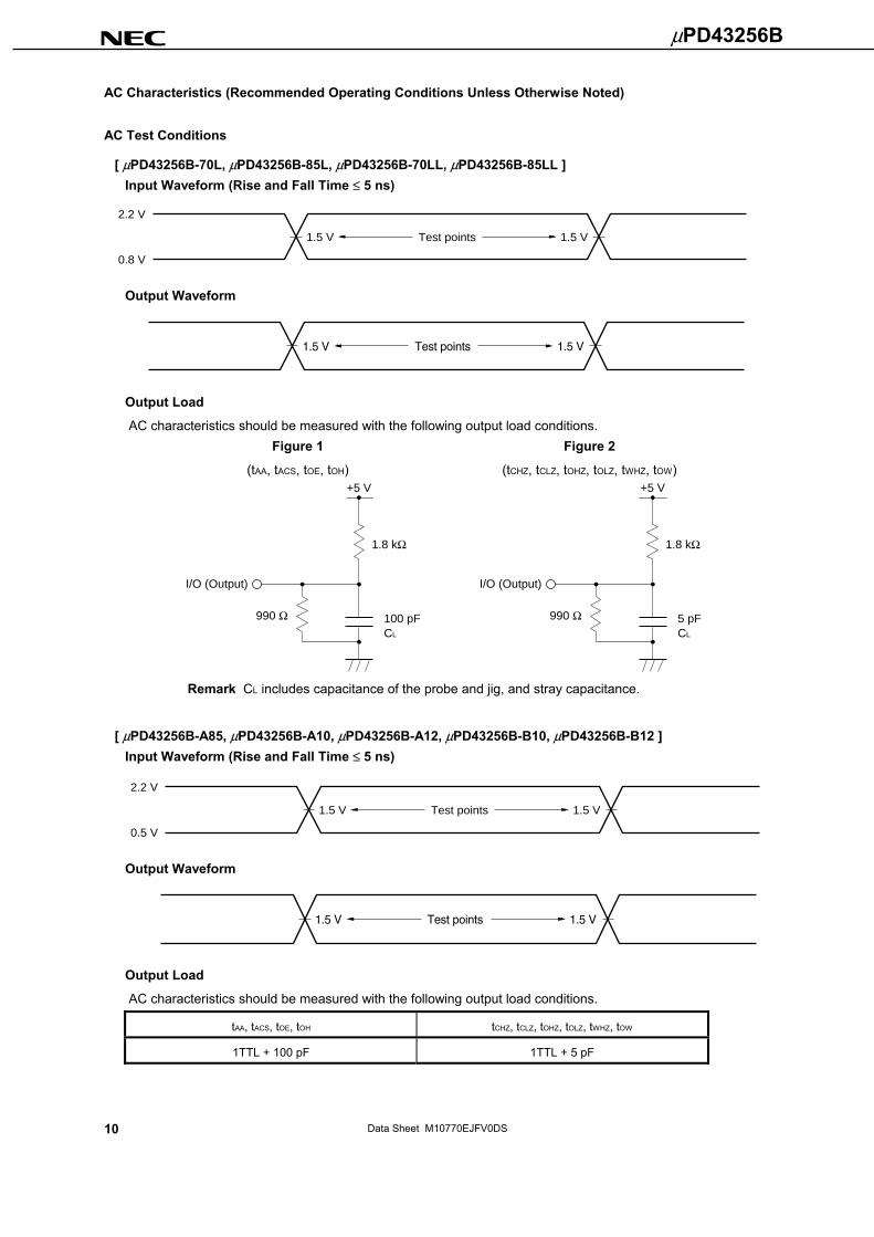
AC Characteristics (Recommended Operating Conditions Unless Otherwise Noted)
AC Test Conditions
[ μPD43256B-70L, μPD43256B-85L, μPD43256B-70LL, μPD43256B-85LL ] Input Waveform (Rise and Fall Time ≤ 5 ns)
Test points
0.8 V
2.2 V
1.5 V 1.5 V
Output Waveform
Output Load
AC characteristics should be measured with the following output load conditions. Figure 1 Figure 2
(tAA, tACS, tOE, tOH) (tCHZ, tCLZ, tOHZ, tOLZ, tWHZ, tOW) +5 V
I/O (Output)
1.8 kΩ
5 pFCL
990 Ω
+5 V
I/O (Output)
1.8 kΩ
100 pFCL
990 Ω
Remark CL includes capacitance of the probe and jig, and stray capacitance.
[ μPD43256B-A85, μPD43256B-A10, μPD43256B-A12, μPD43256B-B10, μPD43256B-B12 ] Input Waveform (Rise and Fall Time ≤ 5 ns)
Test points
0.5 V
2.2 V
1.5 V 1.5 V
Output Waveform
Output Load
AC characteristics should be measured with the following output load conditions.
tAA, tACS, tOE, tOH tCHZ, tCLZ, tOHZ, tOLZ, tWHZ, tOW
1TTL + 100 pF 1TTL + 5 pF
11
μPD43256B
Data Sheet M10770EJFV0DS
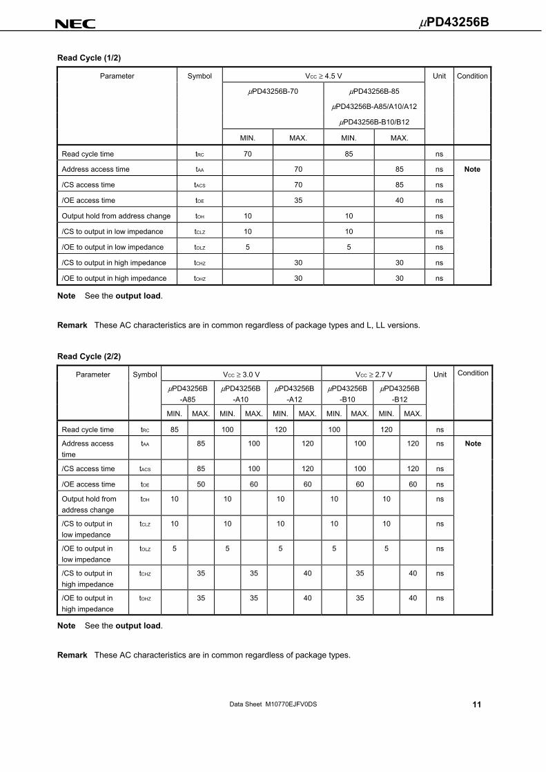
Read Cycle (1/2)
Parameter Symbol VCC ≥ 4.5 V Unit Condition
μPD43256B-70 μPD43256B-85
μPD43256B-A85/A10/A12
μPD43256B-B10/B12
MIN. MAX. MIN. MAX.
Read cycle time tRC 70 85 ns
Address access time tAA 70 85 ns Note
/CS access time tACS 70 85 ns
/OE access time tOE 35 40 ns
Output hold from address change tOH 10 10 ns
/CS to output in low impedance tCLZ 10 10 ns
/OE to output in low impedance tOLZ 5 5 ns
/CS to output in high impedance tCHZ 30 30 ns
/OE to output in high impedance tOHZ 30 30 ns
Note See the output load.
Remark These AC characteristics are in common regardless of package types and L, LL versions.
Read Cycle (2/2)
Parameter Symbol VCC ≥ 3.0 V VCC ≥ 2.7 V Unit Condition
μPD43256B
-A85 μPD43256B
-A10 μPD43256B
-A12 μPD43256B
-B10 μPD43256B
-B12
MIN. MAX. MIN. MAX. MIN. MAX. MIN. MAX. MIN. MAX.
Read cycle time tRC 85 100 120 100 120 ns
Address access time
tAA
85
100
120
100
120
ns
Note
/CS access time tACS 85 100 120 100 120 ns
/OE access time tOE 50 60 60 60 60 ns
Output hold from address change
tOH
10
10
10
10
10
ns
/CS to output in low impedance
tCLZ
10
10
10
10
10
ns
/OE to output in low impedance
tOLZ
5
5
5
5
5
ns
/CS to output in high impedance
tCHZ
35
35
40
35
40
ns
/OE to output in high impedance
tOHZ
35
35
40
35
40
ns
Note See the output load.
Remark These AC characteristics are in common regardless of package types.
12
μPD43256B
Data Sheet M10770EJFV0DS
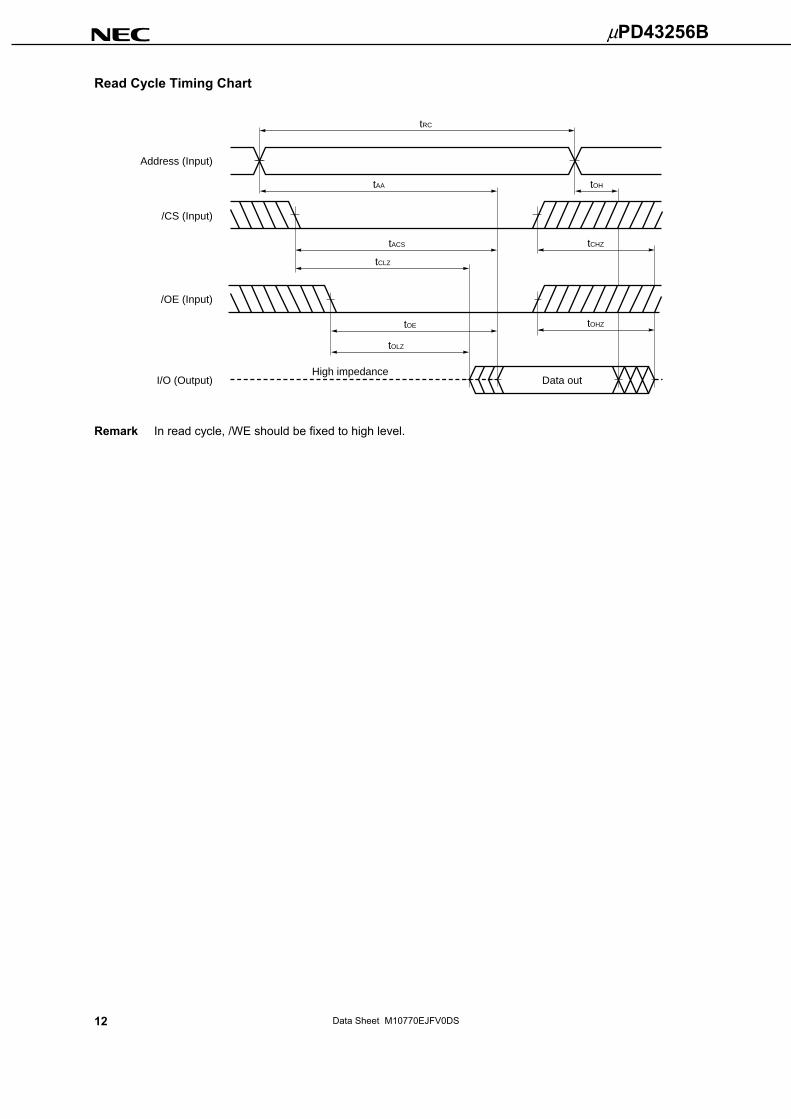
Read Cycle Timing Chart
tOHZ
tRC
tOH
tCHZ
tOLZ
tOE
tCLZ
tACS
tAA
High impedanceData out
/OE (Input)
/CS (Input)
Address (Input)
I/O (Output)
Remark In read cycle, /WE should be fixed to high level.
13
μPD43256B
Data Sheet M10770EJFV0DS
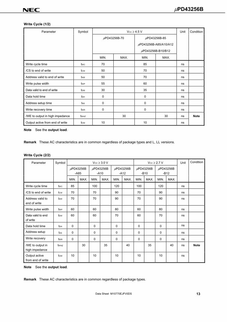
Write Cycle (1/2)
Parameter Symbol VCC ≥ 4.5 V Unit Condition
μPD43256B-70 μPD43256B-85
μPD43256B-A85/A10/A12
μPD43256B-B10/B12
MIN. MAX. MIN. MAX.
Write cycle time tWC 70 85 ns
/CS to end of write tCW 50 70 ns
Address valid to end of write tAW 50 70 ns
Write pulse width tWP 55 60 ns
Data valid to end of write tDW 30 35 ns
Data hold time tDH 0 0 ns
Address setup time tAS 0 0 ns
Write recovery time tWR 0 0 ns
/WE to output in high impedance tWHZ 30 30 ns Note
Output active from end of write tOW 10 10 ns
Note See the output load.
Remark These AC characteristics are in common regardless of package types and L, LL versions.
Write Cycle (2/2)
Parameter Symbol VCC ≥ 3.0 V VCC ≥ 2.7 V Unit Condition
μPD43256B
-A85 μPD43256B
-A10 μPD43256B
-A12 μPD43256B
-B10 μPD43256B
-B12
MIN. MAX. MIN. MAX. MIN. MAX. MIN. MAX. MIN. MAX.
Write cycle time tWC 85 100 120 100 120 ns
/CS to end of write tCW 70 70 90 70 90 ns
Address valid to end of write
tAW
70
70
90
70
90
ns
Write pulse width tWP 60 60 80 60 80 ns
Data valid to end of write
tDW
60
60
70
60
70
ns
Data hold time tDH 0 0 0 0 0 ns
Address setup tAS 0 0 0 0 0 ns
Write recovery tWR 0 0 0 0 0 ns
/WE to output in high impedance
tWHZ
30
35
40
35
40
ns
Note
Output active from end of write
tOW
10
10
10
10
10
ns
Note See the output load.
Remark These AC characteristics are in common regardless of package types.
14
μPD43256B
Data Sheet M10770EJFV0DS
Write Cycle Timing Chart 1 (/WE Controlled)
tWC
tCW
tWHZ tDW tDH
tOW
Indefinite data outHigh
impe-dance
High
impe-dance
Data in Indefinite data out
Address (Input)
/CS (Input)
I/O (Input / Output)
tAW
tWPtAS tWR
/WE (Input)
Cautions 1. /CS or /WE should be fixed to high level during address transition.
2. When I/O pins are in the output state, therefore the input signals must not be applied to
the output.
Remarks 1. Write operation is done during the overlap time of a low level /CS and a low level /WE.
2. When /WE is at low level, the I/O pins are always high impedance. When /WE is at high level,
read operation is executed. Therefore /OE should be at high level to make the I/O pins high
impedance.
3. If /CS changes to low level at the same time or after the change of /WE to low level, the I/O
pins will remain high impedance state.
15
μPD43256B
Data Sheet M10770EJFV0DS
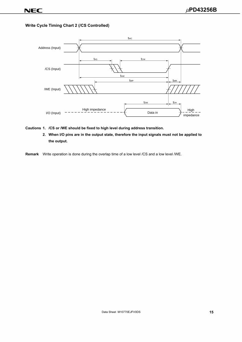
Write Cycle Timing Chart 2 (/CS Controlled)
tWC
tAS tCW
tDW tDH
Data inHigh impedance
Address (Input)
/CS (Input)
I/O (Input)High
impedance
tAW
tWP tWR
/WE (Input)
Cautions 1. /CS or /WE should be fixed to high level during address transition.
2. When I/O pins are in the output state, therefore the input signals must not be applied to
the output.
Remark Write operation is done during the overlap time of a low level /CS and a low level /WE.
16
μPD43256B
Data Sheet M10770EJFV0DS
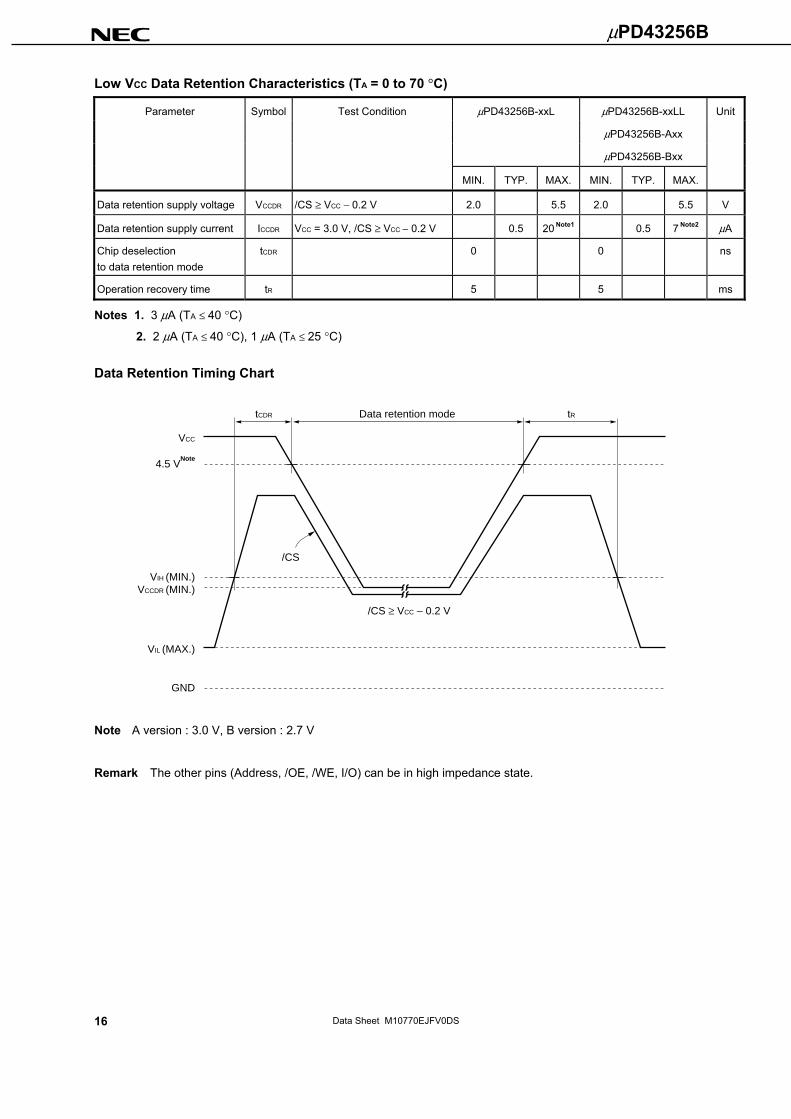
Low VCC Data Retention Characteristics (TA = 0 to 70 °C)
Parameter Symbol Test Condition μPD43256B-xxL μPD43256B-xxLL Unit
μPD43256B-Axx
μPD43256B-Bxx
MIN. TYP. MAX. MIN. TYP. MAX.
Data retention supply voltage VCCDR /CS ≥ VCC − 0.2 V 2.0 5.5 2.0 5.5 V
Data retention supply current ICCDR VCC = 3.0 V, /CS ≥ VCC − 0.2 V 0.5 20 Note1 0.5 7 Note2 μA
Chip deselection to data retention mode
tCDR
0
0
ns
Operation recovery time tR 5 5 ms
Notes 1. 3 μA (TA ≤ 40 °C)
2. 2 μA (TA ≤ 40 °C), 1 μA (TA ≤ 25 °C)
Data Retention Timing Chart
VIH (MIN.)VCCDR (MIN.)
VIL (MAX.)
VCC
/CS
/CS ≥ VCC – 0.2 V
GND
4.5 VNote
tCDR Data retention mode tR
Note A version : 3.0 V, B version : 2.7 V
Remark The other pins (Address, /OE, /WE, I/O) can be in high impedance state.
17
μPD43256B
Data Sheet M10770EJFV0DS
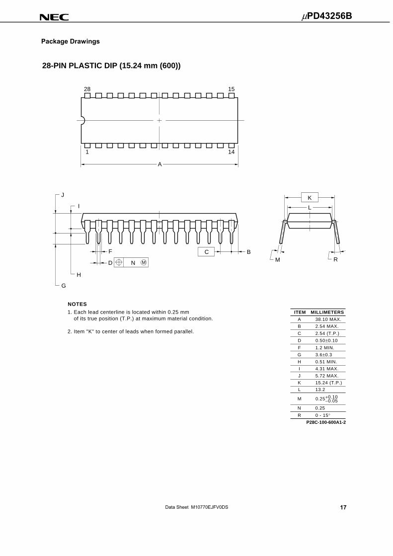
Package Drawings
ITEM MILLIMETERS
A
B
C
F
G
H
I
J
K
38.10 MAX.
2.54 (T.P.)
3.6±0.3
0.51 MIN.
4.31 MAX.
2.54 MAX.
L
0.25
15.24 (T.P.)
5.72 MAX.
13.2
N
1.2 MIN.
P28C-100-600A1-2
D 0.50±0.10
M 0.25+0.10−0.05
R 0 - 15°
NOTES
Each lead centerline is located within 0.25 mmof its true position (T.P.) at maximum material condition.
Item "K" to center of leads when formed parallel.
1.
2.
28
1
15
14
A
M R
K
L
B
J
G
I
CF
D MN
28-PIN PLASTIC DIP (15.24 mm (600))
H
18
μPD43256B
Data Sheet M10770EJFV0DS
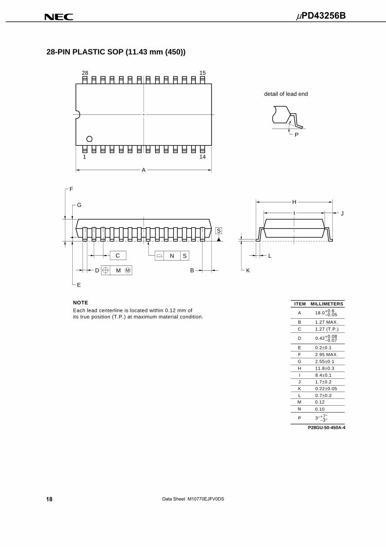
28 15
1 14
S
−3°
ITEM MILLIMETERS
A
B
C
E
F
G
H
J
18.0
1.27 (T.P.)
2.95 MAX.
2.55±0.1
11.8±0.3
1.27 MAX.
0.12
1.7±0.2
M
0.2±0.1
N
P28GU-50-450A-4
P 3°+7°
NOTE
Each lead centerline is located within 0.12 mm ofits true position (T.P.) at maximum material condition.
D 0.42+0.08−0.07
K 0.22±0.05
+0.6−0.05
L 0.7±0.2
0.10
I 8.4±0.1
28-PIN PLASTIC SOP (11.43 mm (450))
M
F
E
D M
C
G
B
L
J
K
P
detail of lead end
A
SN
I
H
19
μPD43256B
Data Sheet M10770EJFV0DS
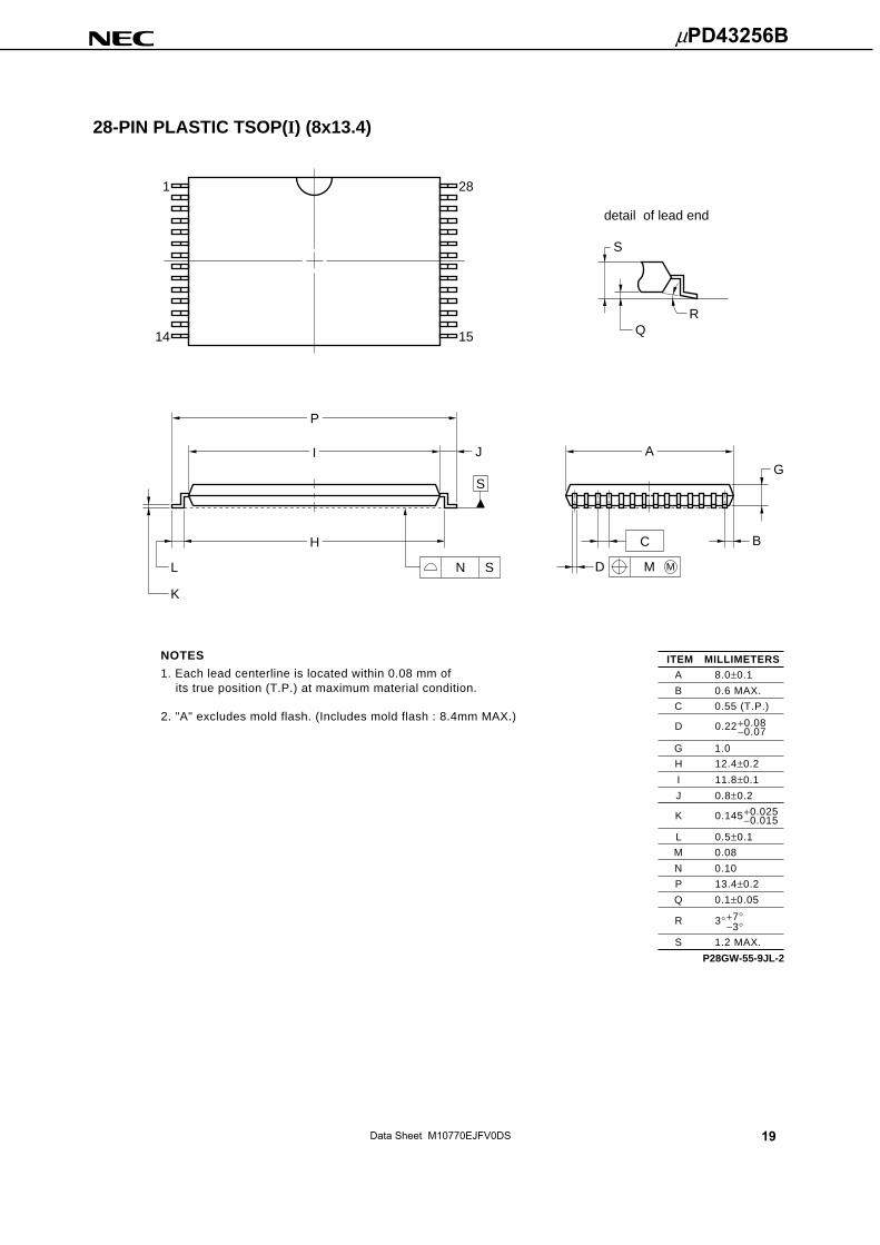
+7°−3°
28-PIN PLASTIC TSOP(I) (8x13.4)
ITEM MILLIMETERSNOTES
1. Each lead centerline is located within 0.08 mm of its true position (T.P.) at maximum material condition.
P28GW-55-9JL-2
M 0.08
N 0.10
H 12.4±0.2
I 11.8±0.1
J 0.8±0.2
S 1.2 MAX.
A 8.0±0.1
B 0.6 MAX.
C 0.55 (T.P.)
G 1.0
K 0.145
L 0.5±0.1
P 13.4±0.2
Q 0.1±0.05
R 3°
D 0.22+0.08−0.07
M
detail of lead end
QR
G
BC
D ML
K
+0.025−0.015
S
2. "A" excludes mold flash. (Includes mold flash : 8.4mm MAX.)
1
14
28
15
SN
S
AJ
P
I
H
20
μPD43256B
Data Sheet M10770EJFV0DS
Recommended Soldering Conditions
Please consult with our sales offices for soldering conditions of the μPD43256B.
Types of Surface Mount Device
μPD43256BGU-xxL : 28-pin PLASTIC SOP (11.43 mm (450))
μPD43256BGU-xxLL : 28-pin PLASTIC SOP (11.43 mm (450))
μPD43256BGU-Axx : 28-pin PLASTIC SOP (11.43 mm (450))
μPD43256BGU-Bxx : 28-pin PLASTIC SOP (11.43 mm (450))
μPD43256BGW-xxLL-9JL : 28-pin PLASTIC TSOP (I) (8x13.4) (Normal bent)
μPD43256BGU-xxL-A : 28-pin PLASTIC SOP (11.43 mm (450))
μPD43256BGU-xxLL-A : 28-pin PLASTIC SOP (11.43 mm (450))
μPD43256BGU-Axx-A : 28-pin PLASTIC SOP (11.43 mm (450))
μPD43256BGU-Bxx-A : 28-pin PLASTIC SOP (11.43 mm (450))
μPD43256BGW-xxLL-9JL-A : 28-pin PLASTIC TSOP (I) (8x13.4) (Normal bent)
Types of Through Hole Mount Device
μPD43256BCZ-xxL : 28-pin PLASTIC DIP (15.24 mm (600))
μPD43256BCZ-xxLL : 28-pin PLASTIC DIP (15.24 mm (600))
Soldering process Soldering conditions
Wave soldering (only to leads) Solder temperature : 260 °C or below,
Flow time : 10 seconds or below
Partial heating method Terminal temperature : 300 °C or below,
Time : 3 seconds or below (Per one lead)
Caution Do not jet molten solder on the surface of package.
21
μPD43256B
Data Sheet M10770EJFV0DS
Revision History
Edition/ Page Type of Description
Date This Previous revision
edition edition
15th edition/ through through Modification Ordering Information revised.
Nov. 2008
22
μPD43256B
Data Sheet M10770EJFV0DS
[ MEMO ]
23
μPD43256B
Data Sheet M10770EJFV0DS
1
2
3
4
VOLTAGE APPLICATION WAVEFORM AT INPUT PIN
Waveform distortion due to input noise or a reflected wave may cause malfunction. If the input of the
CMOS device stays in the area between VIL (MAX) and VIH (MIN) due to noise, etc., the device may
malfunction. Take care to prevent chattering noise from entering the device when the input level is fixed,
and also in the transition period when the input level passes through the area between VIL (MAX) and
VIH (MIN).
HANDLING OF UNUSED INPUT PINS
Unconnected CMOS device inputs can be cause of malfunction. If an input pin is unconnected, it is
possible that an internal input level may be generated due to noise, etc., causing malfunction. CMOS
devices behave differently than Bipolar or NMOS devices. Input levels of CMOS devices must be fixed
high or low by using pull-up or pull-down circuitry. Each unused pin should be connected to VDD or GND
via a resistor if there is a possibility that it will be an output pin. All handling related to unused pins must
be judged separately for each device and according to related specifications governing the device.
PRECAUTION AGAINST ESD
A strong electric field, when exposed to a MOS device, can cause destruction of the gate oxide and
ultimately degrade the device operation. Steps must be taken to stop generation of static electricity as
much as possible, and quickly dissipate it when it has occurred. Environmental control must be
adequate. When it is dry, a humidifier should be used. It is recommended to avoid using insulators that
easily build up static electricity. Semiconductor devices must be stored and transported in an anti-static
container, static shielding bag or conductive material. All test and measurement tools including work
benches and floors should be grounded. The operator should be grounded using a wrist strap.
Semiconductor devices must not be touched with bare hands. Similar precautions need to be taken for
PW boards with mounted semiconductor devices.
STATUS BEFORE INITIALIZATION
Power-on does not necessarily define the initial status of a MOS device. Immediately after the power
source is turned ON, devices with reset functions have not yet been initialized. Hence, power-on does
not guarantee output pin levels, I/O settings or contents of registers. A device is not initialized until the
reset signal is received. A reset operation must be executed immediately after power-on for devices
with reset functions.
POWER ON/OFF SEQUENCE
In the case of a device that uses different power supplies for the internal operation and external
interface, as a rule, switch on the external power supply after switching on the internal power supply.
When switching the power supply off, as a rule, switch off the external power supply and then the
internal power supply. Use of the reverse power on/off sequences may result in the application of an
overvoltage to the internal elements of the device, causing malfunction and degradation of internal
elements due to the passage of an abnormal current.
The correct power on/off sequence must be judged separately for each device and according to related
specifications governing the device.
INPUT OF SIGNAL DURING POWER OFF STATE
Do not input signals or an I/O pull-up power supply while the device is not powered. The current
injection that results from input of such a signal or I/O pull-up power supply may cause malfunction and
the abnormal current that passes in the device at this time may cause degradation of internal elements.
Input of signals during the power off state must be judged separately for each device and according to
related specifications governing the device.
NOTES FOR CMOS DEVICES
5
6
μPD43256B
The information in this document is current as of November, 2008. The information is subject to change without notice. For actual design-in, refer to the latest publications of NEC Electronics data sheets or data books, etc., for the most up-to-date specifications of NEC Electronics products. Not all products and/or types are available in every country. Please check with an NEC Electronics sales representative for availability and additional information.No part of this document may be copied or reproduced in any form or by any means without the prior written consent of NEC Electronics. NEC Electronics assumes no responsibility for any errors that may appear in this document.NEC Electronics does not assume any liability for infringement of patents, copyrights or other intellectual property rights of third parties by or arising from the use of NEC Electronics products listed in this document or any other liability arising from the use of such products. No license, express, implied or otherwise, is granted under any patents, copyrights or other intellectual property rights of NEC Electronics or others.Descriptions of circuits, software and other related information in this document are provided for illustrative purposes in semiconductor product operation and application examples. The incorporation of these circuits, software and information in the design of a customer's equipment shall be done under the full responsibility of the customer. NEC Electronics assumes no responsibility for any losses incurred by customers or third parties arising from the use of these circuits, software and information.While NEC Electronics endeavors to enhance the quality, reliability and safety of NEC Electronics products, customers agree and acknowledge that the possibility of defects thereof cannot be eliminated entirely. To minimize risks of damage to property or injury (including death) to persons arising from defects in NEC Electronics products, customers must incorporate sufficient safety measures in their design, such as redundancy, fire-containment and anti-failure features.NEC Electronics products are classified into the following three quality grades: "Standard", "Special" and "Specific". The "Specific" quality grade applies only to NEC Electronics products developed based on a customer-designated "quality assurance program" for a specific application. The recommended applications of an NEC Electronics product depend on its quality grade, as indicated below. Customers must check the quality grade of each NEC Electronics product before using it in a particular application.
The quality grade of NEC Electronics products is "Standard" unless otherwise expressly specified in NEC Electronics data sheets or data books, etc. If customers wish to use NEC Electronics products in applications not intended by NEC Electronics, they must contact an NEC Electronics sales representative in advance to determine NEC Electronics' willingness to support a given application.
(Note)
•
•
•
•
•
•
M8E 02. 11-1
(1)
(2)
"NEC Electronics" as used in this statement means NEC Electronics Corporation and also includes its majority-owned subsidiaries."NEC Electronics products" means any product developed or manufactured by or for NEC Electronics (as defined above).
Computers, office equipment, communications equipment, test and measurement equipment, audioand visual equipment, home electronic appliances, machine tools, personal electronic equipmentand industrial robots.Transportation equipment (automobiles, trains, ships, etc.), traffic control systems, anti-disastersystems, anti-crime systems, safety equipment and medical equipment (not specifically designedfor life support).Aircraft, aerospace equipment, submersible repeaters, nuclear reactor control systems, lifesupport systems and medical equipment for life support, etc.
"Standard":
"Special":
"Specific":


![CS42448 108 dB, 192 kHz 6-In, 8-Out CODEC · 6 DS648F4 CS42448 1. PIN DESCRIPTIONS Pin Name # Pin Description AD0/CS 1 Address Bit [0]/ Chip Select (Input) - Chip address bit in I²C](https://img.pdfslide.net/doc/110x75/5d62375c88c993e75e8bd078/cs42448-108-db-192-khz-6-in-8-out-6-ds648f4-cs42448-1-pin-descriptions-pin.jpg)