Embed Size (px)
Citation preview

2596 IEEE JOURNAL OF SOLID-STATE CIRCUITS, VOL. 51, NO. 11, NOVEMBER 2016
A Fully Integrated 320 GHz Coherent ImagingTransceiver in 130 nm SiGe BiCMOS
Chen Jiang, Student Member, IEEE, Ali Mostajeran, Student Member, IEEE, Ruonan Han, Member, IEEE,Mohammad Emadi, Hani Sherry, Member, IEEE, Andreia Cathelin, Senior Member, IEEE,
and Ehsan Afshari, Senior Member, IEEE
Abstract— A 320 GHz fully integrated terahertz imagingsystem is reported. The system is composed of a phase-locked high-power transmitter and a coherent high-sensitivitysubharmonic-mixing receiver, which are fabricated using a130 nm SiGe BiCMOS technology ( fT / fmax = 220/280 GHz).To enhance the imaging sensitivity, a heterodyne coherent detec-tion scheme is utilized. To obtain frequency coherency, fullyintegrated phase-locked loops are implemented on both thetransmitter and receiver chips. According to the measurementresults, consuming a total dc power of 605 mW, the transmitterchip achieves a peak radiated power of 2 mW and a peakEIRP of 21.1 dBm. The receiver chip achieves an equivalentincoherent responsivity of more than 7.26 MV/W and a sensitivityof 70.1 pW under an integration bandwidth of 1 kHz, with a totaldc power consumption of 117 mW. The achieved sensitivity withthis proposed coherent imaging transceiver is around ten timesbetter compared with other state-of-the-art incoherent imagers.To the best of our knowledge, this paper demonstrates the firstfully integrated coherent terahertz imaging transceiver on silicon.
Index Terms— BiCMOS, coherent imager, heterodyne detec-tion, phase-locked loop (PLL), return-path gap coupler (RPGC),sensitivity, SiGe, subharmonic mixing, terahertz imaging,transceiver.
I. INTRODUCTION
DUE to the emerging applications in security screening [1],biology [2], medical diagnosis [3], and material char-
acterization [4], terahertz imagers are attracting increasingattention. Compared with microwave frequencies, the shorterwavelength could effectively enhance the spatial resolution.Compared with X-ray, the nonionizing nature makes it morepreferable in many applications. As the development of fab-rication and design techniques, silicon platform is becomingmore and more attractive and suitable for terahertz imagersimplementation, since it could provide much higher integrationlevel and yield, as a result, significantly lower cost and smallersize.
Manuscript received May 17, 2016; revised July 9, 2016; acceptedAugust 2, 2016. Date of publication September 13, 2016; date of currentversion October 29, 2016. This paper was approved by Associate EditorKenichi Okada. This work is supported by Army Research Lab (ARL) andby Army Research Office (ARO).
C. Jiang, A. Mostajeran, and E. Afshari are with the Department ofElectrical and Computer Engineering, Cornell University, Ithaca, NY 14853,USA, and the Department of Electrical Engineering and Computer Science,University of Michigan, Ann Arbor, MI 48109, USA ([email protected]).
R. Han is with the Department of Electrical Engineering and ComputerScience, Massachusetts Institute of Technology, Cambridge, MA 02139 USA.
M. Emadi is with Qualcomm Inc., San Jose, CA 95110 USA.H. Sherry and A. Cathelin are with STMicroelectronics, 38920 Crolles,
France.Color versions of one or more of the figures in this paper are available
online at http://ieeexplore.ieee.org.Digital Object Identifier 10.1109/JSSC.2016.2599533
According to Planck’s law of thermal radiation, terahertzwave is emitted from any warm body as part of the blackbodyradiation [5], but the emitted power is normally very weak.Due to the limited sensitivity of current silicon detectors,the active imaging scheme is more practical, which meansthat a high-power terahertz radiating source is needed forillumination. As a result, a lot of research effort was madeon silicon terahertz source design and significant progresshas been made. In [6], a 280 GHz 4 × 4 radiating arraycapable of beamsteering is presented, which achieves a0.19 mW output power and a 9.4 dBm EIRP. A 338 GHz 2-D4×4 phased array is introduced in [7], and the obtained outputpower and EIRP are 0.81 mW and 17.1 dBm, respectively.In [8], a 530 GHz source module with up to 1 mW outputpower for diffuse illumination is demonstrated. To form acomplete imaging system, a terahertz detector is needed to pairup with the source. Previous works have also demonstratedterahertz detectors on silicon successfully. Using Schottkybarrier diodes, a 280 GHz 4 × 4 array and an 860 GHzdetector cell are demonstrated, achieving minimum NEPs of29 and 42 pW/
√Hz, respectively [9]. In [10], a 320 GHz
4 × 4 imaging array in a SiGe technology is presented, whichis measured to have an average NEP of 34 pW/
√Hz. In [11],
a 1 kpixel terahertz imaging camera chip at 860 GHz isintroduced, which achieves an NEP of 100 pW/
√Hz.
However, since most of the previous works are based onincoherent direct detection, the sensitivity is limited. Con-sequently, in order to obtain a reasonable dynamic range,normally an off-chip high-power source is needed for illu-mination [9]–[11]. In order to implement a fully integratedterahertz imager, the detector sensitivity needs to be improvedto alleviate the output power requirement on the source, sothat an on-chip source would suffice. To enhance the detectorsensitivity, the heterodyne detection scheme can be used [12].However, this requires frequency coherency between thesource and the detector. To achieve this, multiplier-chain-based sources could be used, but they are normally less powerefficient and need RF input sources [13]. Fortunately, thephase-locked terahertz sources on silicon have been demon-strated recently. In [14], a 300 GHz phase-locked loop (PLL)is introduced, which can provide a 40 μW probed outputpower. In [15], a 320 GHz transmitter chip with on-chip PLLachieving a 3.3 mW output power and a 22.5 dBm EIRP isdemonstrated.
In this paper, a 320 GHz coherent imaging transceiver is pre-sented. In the transmitter chip, a 4×4 radiator array is injectionlocked to an on-chip PLL to provide terahertz illumination.
0018-9200 © 2016 IEEE. Personal use is permitted, but republication/redistribution requires IEEE permission.See http://www.ieee.org/publications_standards/publications/rights/index.html for more information.

JIANG et al.: FULLY INTEGRATED 320 GHz COHERENT IMAGING TRANSCEIVER IN 130 nm SiGe BiCMOS 2597
Fig. 1. Principles of (a) incoherent direct detection and (b) coherent heterodyne detection.
In the receiver chip, an eight-cell subharmonic-mixing detectorarray is used to perform a coherent heterodyne detectionto enhance sensitivity. Fabricated with a 130 nm SiGe:CBiCMOS process, the transmitter achieves a 2 mW out-put power and a 21.1 dBm EIRP. The receiver achieves a31 V/V RF-to-baseband voltage conversion gain. With a 1 kHzbandwidth (corresponding to a 1 ms time constant for fastimaging), the proposed coherent imager achieves a sensitivityof 70.1 pW. Compared with other state-of-the-art incoherentimagers, it is around ten times better. The sensitivity enhanceseven further with larger bandwidth (around 20 times for10 kHz and around 70 times for 100 kHz) correspondingto faster imaging. Even though coherent imaging has beendemonstrated previously, all of them use multiplier-chain-based sources [16] or injection lock on-chip sources to outsidesignal [17], which all require high-frequency high-power RFinputs. Using the PLL-based structure, this paper demonstratesthe first fully integrated coherent terahertz imaging transceiveron silicon.
In Section II, principles of the coherent heterodyne detec-tion and the transceiver architecture are introduced. Thetransmitter architecture and detailed circuit blocks designare given in Section III. The subharmonic-mixing receiverdesign is presented in Section IV. The experimental resultsof the imager prototype are presented in Section V. Finally,a performance summary and comparison with some state-of-the-art imagers as well as a brief conclusion are givenin Section VI.
II. PRINCIPLES OF HETERODYNE DETECTION AND
SYSTEM ARCHITECTURE
Due to the limited fmax and breakdown voltage of silicontransistors, obtaining high output power is still challenging.With the current silicon sources, in order to achieve highdynamic range for high-quality imaging, the sensitivity of thedetector needs to be enhanced.
A. Heterodyne Detection and Direct Detection
The conventional incoherent direct detection scheme isshown in Fig. 1(a). If an input signal VRF cos(ωRFt + ϕRF)is applied, the produced dc output change will be a2V 2
RF/2,where a2 is determined by the nonlinear device used. Dueto its simplicity, this scheme is used in most of the previousworks [9]–[11], [18]. To alleviate the impact of the deviceflicker noise, the output signal is normally chopped to anIF frequency. As a result, the output IF signal (fundamental
Fig. 2. ST 130 nm BiCMOS bipolar transistor with a 700 nm emitter lengthconfigured as a (a) direct detector and a (b) heterodyne detector.
tone of the square wave after chopping) is
VIF(t) = 1
πa2V 2
RF cos(ωIFt) (1)
in which ωIF is the chopping frequency. In the heterodynedetection scheme, the input terahertz signal is mixed with alocal oscillation (LO) signal to generate the output IF signal,as shown in Fig. 1(b). In this case, if a terahertz input ofVRF cos(ωRFt +ϕRF) and an LO of VLO cos(ωLOt) are applied,the output IF signal can be written as
VIF(t) = −b2VRFVLO cos(ωIFt + ϕRF) (2)
in which ωIF equals the frequency difference between the RFand LO, ϕRF represents the phase of the RF signal, and b2 isthe mixing coefficient of the device. Comparing (1) and (2), wecan see that in the heterodyne detection case, the followingshold.
1) The output drops with VRF instead of V 2RF, meaning
when the RF signal is weak, the output of a heterodynedetector drops much slower compared with that of a directdetection one.
2) The output signal is also proportional to VLO. Normally,as the LO power is considerably higher than theRF signal, the output signal will also be stronger.
3) Phase information of the RF signal (ϕRF) is preservedat the output. As a result, electrical scanning basedon digital beamforming is achievable, which has thepotential to replace the traditional mechanical scanningto significantly reduce the imaging time.
Therefore, the heterodyne detection scheme can largelyenhance the detector performance. For a further comparison,a bipolar transistor is configured both as a direct detector[input power injected from the emitter, as shown in Fig. 2(a)]and a heterodyne detector [input power injected from theemitter and −20 dBm LO power pumped into the base,

2598 IEEE JOURNAL OF SOLID-STATE CIRCUITS, VOL. 51, NO. 11, NOVEMBER 2016
Fig. 3. Comparison simulation results using the ST 130 nm BiCMOS bipolartransistor.
Fig. 4. PLL-based subharmonic-mixing heterodyne detection transceiverarchitecture.
as shown in Fig. 2(b)]. The simulated output current withdifferent RF powers in both cases is shown in Fig. 3. It isobvious that under low RF power, which is the real scenarioin most applications, the heterodyne detection scheme showsa great advantage. With an assumed bandwidth of 1 MHz,the simulated integrated current noise is 7.7 nA. Under thiscircumstance, to achieve a signal-to-noise ratio (SNR) of 1,the required input power of the heterodyne detector is around40 dB lower than that of the direct detector. If a bandwidthof 10 kHz is chosen, the difference becomes 50 dB, as shownin Fig. 3.
B. Subharmonic-Mixing Heterodyne Transceiver Architecture
The heterodyne detection scheme requires frequencycoherency between the transmitter and the receiver in orderto obtain an output signal with a stable frequency. Frequencycoherency can be obtained using multiplier chains; however,it has two obvious drawbacks: 1) it needs high-power high-frequency sources and 2) the dc-to-RF efficiency is normallylow compared with oscillator-based sources [13]. In orderto achieve higher integration level and better power effi-ciency, a PLL-based transceiver architecture shown in Fig. 4is proposed. In the transmitter, the 320 GHz radiator isinjection locked to a 160 GHz PLL. There is one importantissue that needs to be addressed: the radiator is required togenerate high output power, which needs the oscillators inthe radiator to have a large oscillation activity. However, thepower injected into the radiator is limited due to the powerconsumption restriction of the PLL. As a result, the radiatorcan only be locked within a limited range near its free-runningfrequency [19]. Fortunately, the heterodyne detection scheme
does not require large frequency tuning. However, since thefree-running frequency of the radiator is hard to predict accu-rately due to the inaccurate device model at high frequencyand process variation, the PLL needs to have a sufficienttuning range to cover the possible frequency shift of theradiator. In the receiver, the phase-locked 320 GHz RF signalis mixed with the 160.05 GHz LO generated by the receiverPLL. Ideally, we could use the PLL to injection lock another320 GHz oscillator to generate the LO signal. However, witha large oscillation activity in the 320 GHz oscillator, thetuning range for the LO is largely reduced as discussed before.Due to the possible frequency mismatch caused by processvariation between the transmitter and receiver, such a smalllocking range may not be able to ensure frequency coherency.To address this issue, even with a relatively larger conversionloss, the subharmonic-mixing scheme is still used to obtaina wider LO tuning range to ensure frequency coherency.Moreover, in this scheme, the PLL in the transmitter can bereused in the receiver with minor modifications, which makesit much simpler and also causes less frequency mismatch.After the subharmonic mixing, the output 100 MHz IF signal isthen processed by the on-chip baseband circuits. The detectionoutput is finally collected and sent to a computer for imageconstruction.
III. DESIGN OF THE HIGH-POWER
PHASE-LOCKED TRANSMITTER
Even though the heterodyne detection scheme couldenhance the sensitivity of the detector, it is still desirable toachieve high output power for better image quality. Shownin Fig. 5 is the architecture of the high-power 320 GHzphase-locked transmitter. Sixteen radiator cells form a4 × 4 radiator array with their power adding up in free space.The radiator array is then injection locked by the 160 GHzPLL. A similar architecture is reported in [15]; however, onlya 200 MHz tuning range is achieved at the 320 GHz output.It will be shown later that patch antennas are used on thereceiver side, which have a narrow bandwidth. In order toensure that the transmitted frequency falls inside the receiverantenna bandwidth, a much larger frequency tuning range isdesired. Next, design details of some critical circuit blocks aregiven.
A. Radiator Array
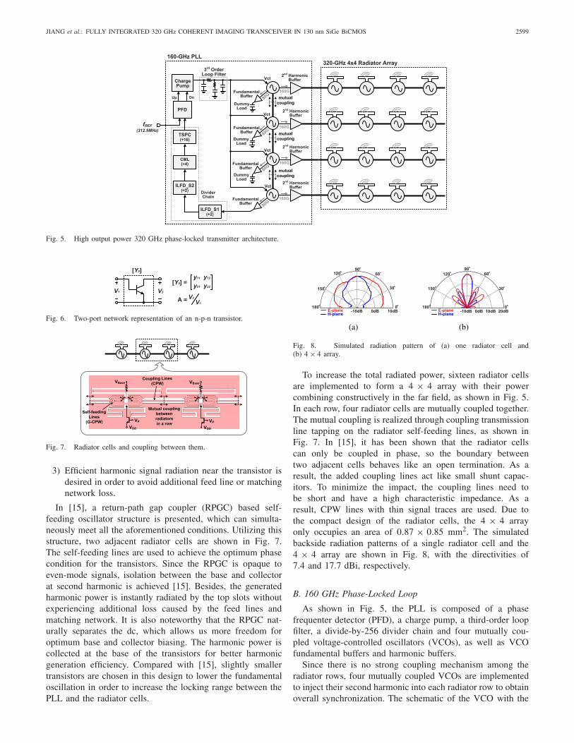
Since the targeted frequency is higher than the fmax ofthe transistors in this 130 nm BiCMOS process ( fmax =280 GHz [20]), harmonic oscillators are used. It has beenshown in [15] that there are several conditions for maximizingthe radiated harmonic power.
1) Shown in Fig. 6 is a two-port network representationof a bipolar transistor. As shown in [21], there is anoptimum phase condition for the complex voltage gain Ato maximize the fundamental oscillation activity: � Aopt =� − (y21 + y∗
12).2) Isolation between the base and collector of the transistor
at the desired harmonic frequency is necessary to elimi-nate the self-power-cancellation/loading effect [21].
JIANG et al.: FULLY INTEGRATED 320 GHz COHERENT IMAGING TRANSCEIVER IN 130 nm SiGe BiCMOS 2599
Fig. 5. High output power 320 GHz phase-locked transmitter architecture.
Fig. 6. Two-port network representation of an n-p-n transistor.
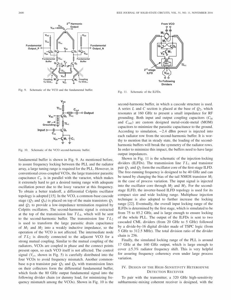
Fig. 7. Radiator cells and coupling between them.
3) Efficient harmonic signal radiation near the transistor isdesired in order to avoid additional feed line or matchingnetwork loss.
In [15], a return-path gap coupler (RPGC) based self-feeding oscillator structure is presented, which can simulta-neously meet all the aforementioned conditions. Utilizing thisstructure, two adjacent radiator cells are shown in Fig. 7.The self-feeding lines are used to achieve the optimum phasecondition for the transistors. Since the RPGC is opaque toeven-mode signals, isolation between the base and collectorat second harmonic is achieved [15]. Besides, the generatedharmonic power is instantly radiated by the top slots withoutexperiencing additional loss caused by the feed lines andmatching network. It is also noteworthy that the RPGC nat-urally separates the dc, which allows us more freedom foroptimum base and collector biasing. The harmonic power iscollected at the base of the transistors for better harmonicgeneration efficiency. Compared with [15], slightly smallertransistors are chosen in this design to lower the fundamentaloscillation in order to increase the locking range between thePLL and the radiator cells.
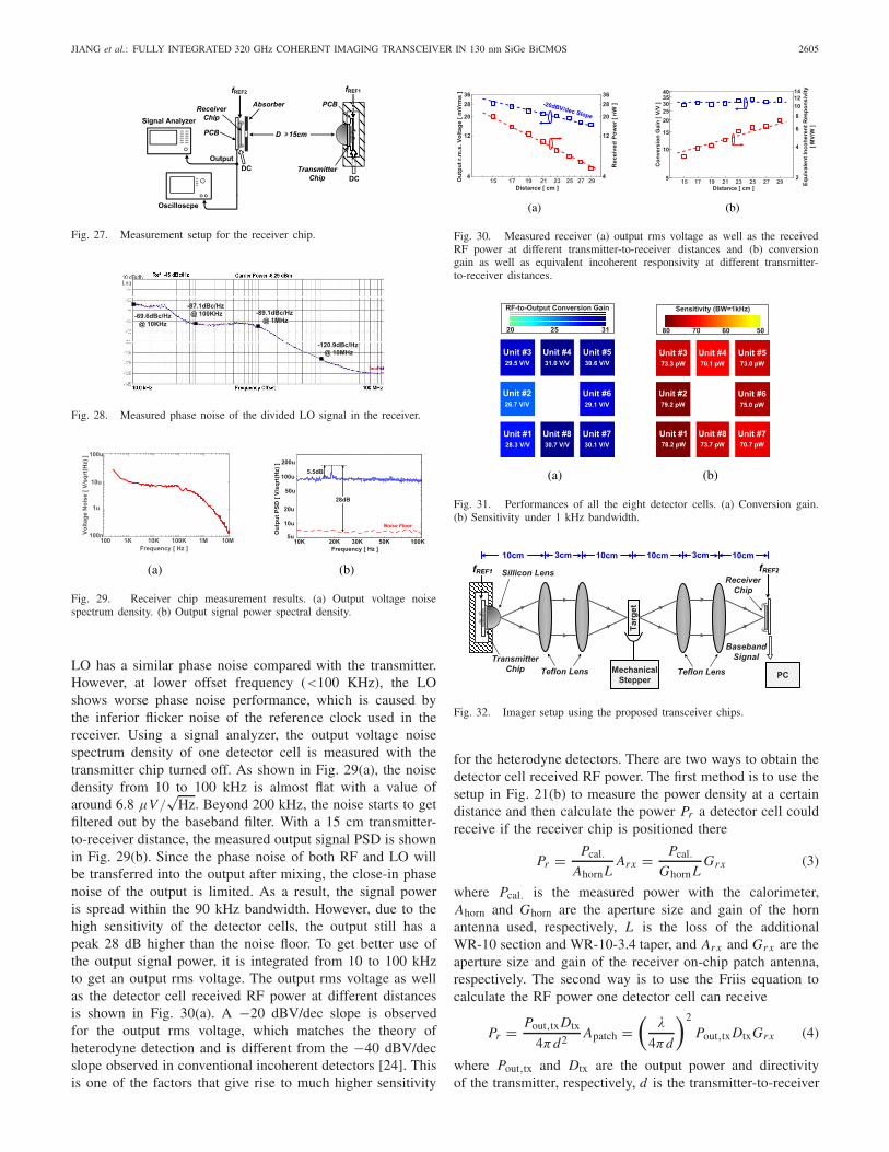
Fig. 8. Simulated radiation pattern of (a) one radiator cell and(b) 4 × 4 array.
To increase the total radiated power, sixteen radiator cellsare implemented to form a 4 × 4 array with their powercombining constructively in the far field, as shown in Fig. 5.In each row, four radiator cells are mutually coupled together.The mutual coupling is realized through coupling transmissionline tapping on the radiator self-feeding lines, as shown inFig. 7. In [15], it has been shown that the radiator cellscan only be coupled in phase, so the boundary betweentwo adjacent cells behaves like an open termination. As aresult, the added coupling lines act like small shunt capac-itors. To minimize the impact, the coupling lines need tobe short and have a high characteristic impedance. As aresult, CPW lines with thin signal traces are used. Due tothe compact design of the radiator cells, the 4 × 4 arrayonly occupies an area of 0.87 × 0.85 mm2. The simulatedbackside radiation patterns of a single radiator cell and the4 × 4 array are shown in Fig. 8, with the directivities of7.4 and 17.7 dBi, respectively.
B. 160 GHz Phase-Locked Loop
As shown in Fig. 5, the PLL is composed of a phasefrequenter detector (PFD), a charge pump, a third-order loopfilter, a divide-by-256 divider chain and four mutually cou-pled voltage-controlled oscillators (VCOs), as well as VCOfundamental buffers and harmonic buffers.
Since there is no strong coupling mechanism among theradiator rows, four mutually coupled VCOs are implementedto inject their second harmonic into each radiator row to obtainoverall synchronization. The schematic of the VCO with the
2600 IEEE JOURNAL OF SOLID-STATE CIRCUITS, VOL. 51, NO. 11, NOVEMBER 2016
Fig. 9. Schematic of the VCO and the fundamental buffer.
Fig. 10. Schematic of the VCO second-harmonic buffer.
fundamental buffer is shown in Fig. 9. As mentioned before,to assure frequency locking between the PLL and the radiatorarray, a large tuning range is required for the PLL. However, inconventional cross-coupled VCOs, the large transistor parasiticcapacitance Cπ is in parallel with the varactor, which makesit extremely hard to get a desired tuning range with adequateoscillation power due to the lossy varactor at this frequency.To obtain a better tradeoff, a differential Colpitts oscillatortopology is adopted [15]. In the VCO, a common-base cascodestage (Q3 and Q4) is placed on top of the main transistors Q1and Q2 to provide a low-impedance termination required byColpitts oscillators. The second-harmonic signal is extractedat the top of the transmission line T L4, which will be sentto the second-harmonic buffer. The transmission line T L2is used to transform the large parasitic drain capacitanceof M1 and M2 into a weakly inductive impedance, so theoperation of the VCO is not affected. The intermediate nodeof T L2 is directly connected to the adjacent VCO for astrong mutual coupling. Similar to the mutual coupling of theradiators, VCOs are coupled in phase and the connect pointspresent open, so each VCO itself is not affected. The controlsignal (Vct , shown in Fig. 5) is carefully distributed into thefour VCOs to avoid frequency mismatch. Another common-base n-p-n transistor pair Q5 and Q6 with transmission lineson their collectors form the differential fundamental buffer,which feeds the 80 GHz output fundamental signal into thefollowing divider chain (or dummy load, for minimizing fre-quency mismatch among the VCOs). Shown in Fig. 10 is the
Fig. 11. Schematic of the ILFDs.
second-harmonic buffer, in which a cascode structure is used.A series L and C section is placed at the base of Q2, whichresonates at 160 GHz to present a small impedance for RFgrounding. Both input and output coupling capacitors (Cinand Cout) are custom designed metal-oxide-metal (MOM)capacitors to minimize the parasitic capacitance to the ground.According to simulation, −2.4 dBm power is injected intoeach radiator row from the second-harmonic buffer. It is wor-thy to mention that in steady state, the loading of the second-harmonic buffers will break the symmetry of the radiator rows.In order to minimize this impact, the buffers need to have largeoutput impedances.
Shown in Fig. 11 is the schematic of the injection-lockingdividers (ILFDs). The transmission line T L1 and transistorpair Q1 and Q2 form the oscillator core of the first-stage ILFD.The free-running frequency is designed to be 40 GHz and canbe tuned by changing the bias of the tail NMOS transistor M1in the case of process variation. The input signal is injectedinto the oscillator core through M2 and M3. For the second-stage ILFD, the inverter-based ILFD topology is used for itscompact size and wide locking range. Multiphase injectiontechnique is also adopted to further increase the lockingrange [22]. Eventually, the overall input locking range of theILFDs is determined by the first stage, which is simulated to befrom 75 to 85.2 GHz, and is large enough to ensure lockingof the whole PLL. The output of the ILFDs is sent to twocascaded CML dividers (from 20 GHz to 5 GHz) followedby a divide-by-16 digital divider made of TSPC logic (from5 GHz to 312.5 MHz). The total division ratio of the dividerchain is 256.
Finally, the simulated locking range of the PLL is around17 GHz at the 160 GHz output, which is large enough tocover ±5.3% radiator frequency shift. This is very helpfulfor assuring frequency coherency even under large processvariation.
IV. DESIGN OF THE HIGH-SENSITIVITY HETERODYNE
DETECTION RECEIVER
To pair with the transmitter, a 320 GHz high-sensitivitysubharmonic-mixing coherent receiver is designed, with the

JIANG et al.: FULLY INTEGRATED 320 GHz COHERENT IMAGING TRANSCEIVER IN 130 nm SiGe BiCMOS 2601
Fig. 12. Subharmonic-mixing heterodyne detection receiver architecture.
architecture shown in Fig. 12. It is composed of an eight-celldetector array, a 160 GHz PLL, and an LO distribution net-work. Using the subharmonic-mixing scheme, the output of thePLL is directly used as the LO signal. In this way, lower powerconsumption and a much wider LO tuning range are achieved.In this section, some design details will be discussed.
A. Subharmonic-Mixing Heterodyne Detector Cell
The structure of the proposed subharmonic-mixing hetero-dyne detector cell is shown in Fig. 13, in which bipolartransistors are used to perform the LO and RF mixing. Thereceived RF signal is injected into the emitter of the transistorsand the LO signal is fed from their base. The detector cellis made into a differential form in order to alleviate the LOself-mixing problem. After LO and RF mixing, the generatedIF signal is amplified by a low-noise preamplifier before itgets mixed again into the 100 kHz baseband signal. Finally alow-pass filter with a 200 kHz cutoff frequency is followed tofilter out the unwanted components.
To accommodate to the differential detector structure,a differential patch antenna is designed. The top and cross-sectional views of the antenna are shown in Fig. 14(a) and (b),respectively. The antenna occupies an area of 250×240 μm2.The antenna is implemented using the top metal (M6), whichhas a thickness of 3 μm. To avoid the terahertz wavefrom coupling into the lossy silicon substrate, an overlappedM1-to-M3 ground plane is placed underneath the antenna. Thedistance between the antenna to the ground plane is 7.61 μm.To avoid crosstalking with the near-by structures (transmissionlines, transistors, etc.), stacked M1-to-M6 metal walls are
Fig. 13. Structure of the subharmonic-mixing heterodyne detector cell.
Fig. 14. Differential patch antenna. (a) Top view. (b) Cross section.(c) Simulated antenna gain in different directions. (d) Simulated reflectioncoefficient versus frequency (Zin = 350 �).
placed surrounding the antenna with a 20 μm clearance.Though the ground walls slightly degrade the efficiency ofthe antenna, adding them provides us with better predictionof the antenna resonance frequency, which is very importantdue to the narrow bandwidth of the patch antennas. As shownin Fig. 13, the emitter of the transistors is directly connectedto the antenna. To provide a dc bias, the center of the patchantenna is connected to ground as shown in Fig. 14(a) and (b).Due to the differential structure, the central line of the antennais equivalently RF grounded, so this ground connection hasno impact. The length of the antenna is set to be 212 μmfor a resonance at 320 GHz, and the width is designed to be200 μm to obtain an impedance of 350 � for easy matchingwith the input impedance at the emitter. The simulated antennagain in different directions and the reflection coefficient versusfrequency are shown in Fig. 14(c) and (d), respectively. Theantenna gain in the broadside is simulated to be 2.2 dB.
To minimize the RF signal loss, the transistors are placedas close to the antenna as possible, with a very simple

2602 IEEE JOURNAL OF SOLID-STATE CIRCUITS, VOL. 51, NO. 11, NOVEMBER 2016
Fig. 15. RF matching at emitter. (a) Matching scheme on a Smith chart.(b) Simulated reflection coefficient versus frequency.
Fig. 16. LO matching at base. (a) Matching scheme on a Smith chart.(b) Simulated reflection coefficient versus frequency.
matching scheme: only one shunt transmission line stub (T L1)is used as shown in Fig. 13. The matching scheme on a Smithchart is shown in Fig. 15(a). The 86 μm shunt stub T L1transforms the emitter impedance of (194-j190) � into 350 �for matching with the patch antenna. To make this matchingscheme feasible, a codesign is needed for the antenna and thetransistors in order to obtain suitable impedances. Besides that,a tradeoff between the conversion loss and the device noisealso needs to be considered while choosing the transistor size.The simulation result of the RF reflection coefficient at thetransistor emitter (assuming a source impedance of 350 �) isshown in Fig. 15(b). In the detector cell, all the transmissionlines are made of G-CPW lines with a characteristic impedanceof 58 �. The matching scheme for the LO signal is shownin Fig. 16(a). The transmission line section T L2 and theshort matching stub T L3 transform the capacitive transistorbase input impedance into a 58 � impedance, so that it isperfectly matched with the characteristic impedance of thefeed line T L4. The dc bias for the base of the transistors isprovided at the far end of T L3. Then, the feed lines (T L4) onthe two sides combine to form a common LO feed-in point,which has an input impedance (ZLO,in) of 29 �. The simulatedLO reflection coefficient at this feed-in point (assuming asource impedance of 29 �) is shown in Fig. 16(b).
B. 160 GHz Phase-Locked Loop
The PLL in the receiver is very similar to the one in thetransmitter, but it has only one VCO, as shown in Fig. 12.In addition, high output impedance is no longer requiredfor the VCO second-harmonic buffer, so it can be modified
Fig. 17. Highly symmetrical LO distribution network structure.
to maximize the delivered LO power. The simulated outputtuning range is 18.1 GHz at the 160 GHz output, which isslightly larger than the one in the transmitter.
C. Highly Symmetrical LO Distribution Network
As shown in Fig. 12, the LO signal generated by thePLL needs to be delivered into each of the eight detectorcells. However, to distribute the LO power evenly with thesame delay (phase) and power is challenging. In order toachieve that, a highly symmetrical distribution network shownin Fig. 17 is designed. First, the LO feed-in points of everytwo adjacent detector cells are combined together with twoS1 blocks, forming four adjoint points. Then, four S2 blockscombines the four newly formed adjoint points together to geta common LO feed-in point for all the eight detector cells.Since the network is mainly built up upon S1 and S2 as wellas their flipped and rotated versions, it is highly symmetrical,which is very helpful for the eight detector cells to receive anLO signal with the same power and phase.
In the S1 block, a 38 � quarter-wave line transforms the29 � detector cell LO port impedance into a 50 � impedance(Z1 = 50 �). After two adjacent detector LO ports arecombined, the impedance seen from each of the adjoint pointswill be Z2 = Z1/2 = 25 �. Then, in the S2 block, another38 � quarter-wave line T L2 transforms Z2 into a 60 �impedance, so the length of the following 60 � line T L3can be adjusted according to the desired distance betweenthe detector cells. After the four S2 blocks join together,the impedance seen at the common LO feed-in point will beZ5 = Z4/4 = 15�. Then, a 38 � and a 60 � quarter-waveline (T L4 and T L5) further transform the impedance into 40 �(Z7 = 40�), as shown in Fig. 17. Assuming that 0 dBm signalpower is applied at the input port of the distribution network,the simulated power and phase shift at all the eight output ports

JIANG et al.: FULLY INTEGRATED 320 GHz COHERENT IMAGING TRANSCEIVER IN 130 nm SiGe BiCMOS 2603
Fig. 18. Simulation results of the LO distribution network.
Fig. 19. Matching network at the output of the 160 GHz PLL. (a) Structure.(b) Matching scheme on a Smith chart.
are shown in Fig. 18. The LO power is evenly distributed withonly a 0.15 dB difference among eight output ports. The totalloss of this distribution network is 1.5 dB. Phase of the upperfour outputs (P1–P4 in Fig. 17) is around 5° behind the lowerfour outputs (P5–P8), this is because the transmission linetapping to the center of the network (T L4 in Fig. 17) slightlybreaks the symmetry. Fortunately, this phase difference causesonly a constant phase offset, which can be easily calibrated.
The simulated optimal load for the VCO harmonic buffer is200 �, so a short-stub matching structure is used to transformthe 40 � input impedance of the LO distribution network into200 �, as shown in Fig. 19. The 40 � feed line betweenthe LO distribution network and this matching structure canhave an arbitrary length, providing more freedom for floorplanof the whole chip. Finally, the LO power delivered into eachdetector cell is simulated to be −12 dBm.
V. PROTOTYPE AND EXPERIMENTAL RESULTS
The proposed coherent imaging transceiver chips are fabri-cated using the STMicroelectronics 130 nm SiGe:C BiCMOSprocess. The transmitter chip shown in Fig. 20(a) occupies anarea of 1.6 × 1.3 mm2. The receiver chip shown in Fig. 20(b)takes an area of 1.7 × 1.8 mm2.
A. Transmitter Measurements
Since the transmitter chip radiates from the backside, toeliminate the lossy substrate wave, a high-resistivity hemi-spherical silicon lens is used [21]. For ease of packaging andalignment, a high resistivity silicon wafer (300 μm thick and∼1 cm2 large) is placed in between the chip and the sili-con lens [23]. The frequency/spectrum measurement setup is
Fig. 20. Microphotograph of the (a) transmitter chip and (b) receiver chip.
shown in Fig. 21(a), in which an even harmonic mixer (EHM)mixes the received THz beam with the 16th harmonic of the20 GHz signal supplied by the signal source. The IF productis then measured with the spectrum analyzer. The measured IFspectrum with the PLL on and off is shown in Fig. 22. Whenthe PLL is off, there is no strong coupling among the radiatorrows, multiple peaks are observed [Fig. 22(a)]. The numberof the peaks does not equal to the number of the radiatorrows, which is caused by the mutual pulling among the rowsthrough the silicon substrate and antenna coupling. When thePLL is turned on, the radiator rows get synchronized throughthe mutually coupled VCOs and only a single peak is observed[Fig. 22(b)]. For a better comparison, a close-in spectrum ofthe free-running scenario and frequency locked scenario areplotted in the same graph, as shown in Fig. 23. It is obviousthat after the frequency locking, the spectrum of the radiatedTHz beam is determined by the PLL, which presents a muchsharper tone compared with the free-running case. The phasenoise after the frequency locking is also shown in Fig. 23.Due to the large division ratio (N = 1024 from 312.5 MHzto 320 GHz) and the wide tuning range requirement forthe PLL, the output phase noise is sacrificed. The measuredin-band (100 kHz offset) and out-of-band (10 MHz offset)phase noises are −67.4 and −87.2 dBc/Hz, respectively. Thefrequency locking range of the transmitter under differentradiator base bias voltages is shown in Fig. 24. As the biasvoltage increases, the oscillation activity of the radiators alsoincreases, and as discussed before, the locking range decreasesquickly. However, a total locking range of 3.91 GHz is stillachieved, which is largely improved compared with [15].
The radiation pattern of the transmitter shown in Fig. 25 ismeasured by rotating the chip in both azimuth and elevationdirections on a rotary stage. The measured directivity is18.0 dBi. It is noteworthy that the insertion of the siliconwafer makes the chip not exactly at the spherical center ofthe lens, which will lead to beam collimation. This explainswhy we observe lower side lobe level in Fig. 25 compared withthe simulation in Fig. 8(b). However, due to the concentratedbeam radiated by the radiator array, the measured directivityis still close to the simulation [23]. The power measurementsetup is shown in Fig. 21(b), in which a PM4 calorimeter isused for better precision. To obtain accurate results, we need tomake sure that the horn antenna is put far away enough from

2604 IEEE JOURNAL OF SOLID-STATE CIRCUITS, VOL. 51, NO. 11, NOVEMBER 2016
Fig. 21. Transmitter measurement setups. (a) Frequency/spectrum measurement setup. (b) Power measurement setup.
Fig. 22. Measured spectrum of the downconverted transmitter radiation when(a) PLL is off and (b) PLL is on.
Fig. 23. Close-in free-running and frequency-locked spectrum of thedownconverted transmitter radiated signal and the phase noise of it afterfrequency locking.
the transmitter to ensure far-field condition and avoid standingwave effect so that the Friis equation is valid. First, thedistance is changed from 5 to 12 cm, the calorimeter measuredpower is shown in Fig. 26(a). It can be seen that when thedistance is larger than 6 cm, the results match with the Friisequation well. In the following measurements, a 9 cm distanceis chosen. The supply voltage for the transmitter is swept,and the peak radiated power and the associated dc-to-THz-radiation efficiency are shown in Fig. 26(b). The maximumradiated power and EIRP achieved are 2 mW and 21.1 dBm,respectively. The maximum dc-to-THz-radiation efficiencyis 2.4%.
The transmitter chip consumes a total dc power of 605 mW:the radiator array dissipates 433 mW, the VCO array (includ-ing fundamental buffers and harmonic buffers) takes 128 mW,and the rest of the PLL consumes a 44 mW power.
B. Receiver Measurements
The measurement setup for the receiver is shown inFig. 27. The transmitter chip works as the source to radiatethe 320 GHz RF signal. To eliminate the standing wave
Fig. 24. Measured frequency locking range under different radiator biaspoints.
Fig. 25. Measured radiation pattern of the transmitter.
Fig. 26. Power measurement results. (a) Measured power by the calorimeterat different distances from the transmitter chip. (b) Measured peak outputpower and the associated dc-to-THz radiation efficiency under different supplyvoltages.
effect caused by reflection at the receiver PCB, an absorberis positioned in front of it with a hole for the wave to passthrough. Even with the absorber, the receiver still needs tobe put at least 15 cm away from the transmitter. The signalanalyzer and the oscilloscope are used to observe the receiveroutput signal in frequency and time domains, respectively.Fig. 28 shows the measured phase noise of the CML outputsignal in the receiver PLL (test point in Fig. 12). Since it isthe LO signal divided by 32, the phase noise of the LO is30 dB higher. At a large offset frequency (>1 MHz), the
JIANG et al.: FULLY INTEGRATED 320 GHz COHERENT IMAGING TRANSCEIVER IN 130 nm SiGe BiCMOS 2605
Fig. 27. Measurement setup for the receiver chip.
Fig. 28. Measured phase noise of the divided LO signal in the receiver.
Fig. 29. Receiver chip measurement results. (a) Output voltage noisespectrum density. (b) Output signal power spectral density.
LO has a similar phase noise compared with the transmitter.However, at lower offset frequency (<100 KHz), the LOshows worse phase noise performance, which is caused bythe inferior flicker noise of the reference clock used in thereceiver. Using a signal analyzer, the output voltage noisespectrum density of one detector cell is measured with thetransmitter chip turned off. As shown in Fig. 29(a), the noisedensity from 10 to 100 kHz is almost flat with a value ofaround 6.8 μV/
√Hz. Beyond 200 kHz, the noise starts to get
filtered out by the baseband filter. With a 15 cm transmitter-to-receiver distance, the measured output signal PSD is shownin Fig. 29(b). Since the phase noise of both RF and LO willbe transferred into the output after mixing, the close-in phasenoise of the output is limited. As a result, the signal poweris spread within the 90 kHz bandwidth. However, due to thehigh sensitivity of the detector cells, the output still has apeak 28 dB higher than the noise floor. To get better use ofthe output signal power, it is integrated from 10 to 100 kHzto get an output rms voltage. The output rms voltage as wellas the detector cell received RF power at different distancesis shown in Fig. 30(a). A −20 dBV/dec slope is observedfor the output rms voltage, which matches the theory ofheterodyne detection and is different from the −40 dBV/decslope observed in conventional incoherent detectors [24]. Thisis one of the factors that give rise to much higher sensitivity
Fig. 30. Measured receiver (a) output rms voltage as well as the receivedRF power at different transmitter-to-receiver distances and (b) conversiongain as well as equivalent incoherent responsivity at different transmitter-to-receiver distances.
Fig. 31. Performances of all the eight detector cells. (a) Conversion gain.(b) Sensitivity under 1 kHz bandwidth.
Fig. 32. Imager setup using the proposed transceiver chips.
for the heterodyne detectors. There are two ways to obtain thedetector cell received RF power. The first method is to use thesetup in Fig. 21(b) to measure the power density at a certaindistance and then calculate the power Pr a detector cell couldreceive if the receiver chip is positioned there
Pr = Pcal.
AhornLArx = Pcal.
Ghorn LGrx (3)
where Pcal. is the measured power with the calorimeter,Ahorn and Ghorn are the aperture size and gain of the hornantenna used, respectively, L is the loss of the additionalWR-10 section and WR-10-3.4 taper, and Arx and Grx are theaperture size and gain of the receiver on-chip patch antenna,respectively. The second way is to use the Friis equation tocalculate the RF power one detector cell can receive
Pr = Pout,txDtx
4πd2 Apatch =(
λ
4πd
)2
Pout,tx DtxGrx (4)
where Pout,tx and Dtx are the output power and directivityof the transmitter, respectively, d is the transmitter-to-receiver

2606 IEEE JOURNAL OF SOLID-STATE CIRCUITS, VOL. 51, NO. 11, NOVEMBER 2016
Fig. 33. Images formed by the imager using the proposed transceiver. (a) Human tooth (130 × 80 pixels). (b) Floppy disk (150 × 140 pixels). (c) StudentID card with a metallic “UNIC” symbol attached to it (150 × 66) pixels.
distance, and Grx is the gain of the receiver antenna. In ourmeasurement, we adopted the first method and verified theresults with the second method. The results are consistent withonly minor differences. Assuming a 50 � impedance for theRF signal, a conversion gain from the received RF rms voltageto output rms voltage can be calculated using
Gv = Vrms√Pr · 50 �
(5)
where Vrms is the output rms voltage and Pr is the receivedRF power. The conversion gain at different distances is shownin Fig. 30(b). The averaged conversion gain is 31.0 V/V.To compare with incoherent detectors, an equivalent inco-herent responsivity is defined as the responsivity that anincoherent detector needs to generate the same output rmsvoltage with the same received RF power. This equivalentresponsivity can be derived with [24]
�v = πVrms√2Pr
. (6)
The receiver equivalent responsivity at different distances isalso shown in Fig. 30(b). It is observed that as the receivedpower decreases, the receiver equivalent incoherent responsiv-ity increases. This also reflects the effectiveness of enhancingdetection sensitivity using heterodyne detection. To make afair comparison between coherent and incoherent imagers,a sensitivity is defined as the received RF power for theoutput signal to have SNR = 1 within a 1 kHz bandwidth(corresponding to 1 ms time constant for fast imaging). Thesensitivity of the proposed receiver is calculated to be 70.1 pW,which is around ten times better compared with other state-of-the-art silicon detectors (as shown in Table III). The sensitivityenhances even further with a larger bandwidth (about 20 timesfor 10 kHz bandwidth and 70 times for 100 kHz bandwidth)corresponding to faster imaging. The measured conversiongain and sensitivity for all the eight detector cells are shownin Fig. 31. Thanks to the highly symmetrical LO distributionnetwork, the performances of the detector cells are quiteuniform.
C. Imager Experiments
To put the transceiver into real use, a transmission modeterahertz imager is built up as shown in Fig. 32, which iscomposed of the transceiver chips, four Teflon lenses, and amechanical stepper. The first two Teflon lenses are used to
TABLE I
PERFORMANCE SUMMARY OF THE TRANSMITTER
TABLE II
PERFORMANCE SUMMARY OF THE RECEIVER
focus the terahertz beam generated by the transmitter chip andform a focal plane. The two Teflon lenses on the receiver sideare used to refocus the transmitted beam in order to increasethe power that could be received by the receiver chip. Themechanical stepper is used to move the object on the focalplane for scanning. With this imager, a few terahertz imagesare formed, as shown in Fig. 33.
VI. CONCLUSION
The performances of the proposed transmitter and receiverchip are summarized in Tables I and II, respectively. Thetransmitter chip achieves a peak radiated power of 2 mW anda peak EIRP of 21.1 dBm with a total dc power consump-tion of 605 mW. The receiver chip achieves an equivalentincoherent responsivity of more than 7.26 MV/W and asensitivity of 70.1 pW under an integration bandwidth of1 kHz. The total dc power consumption of the receiver chip is117 mW. A comparison with other terahertz imagers is givenin Table III. It can be seen that under the 1 kHz integrationbandwidth, the proposed coherent imager can achieve around

JIANG et al.: FULLY INTEGRATED 320 GHz COHERENT IMAGING TRANSCEIVER IN 130 nm SiGe BiCMOS 2607
TABLE III
COMPARISON WITH PREVIOUS STATE-OF-THE-ART WORKS
ten times better sensitivity compared with other state-of-the-artincoherent ones. Using the PLL-based architecture, no off-chiphigh-frequency high-power sources are needed. To our bestknowledge, this paper demonstrates the first fully integratedcoherent terahertz imaging transceiver on silicon.
ACKNOWLEDGMENT
The authors would like to thank STMicroelectronics for thechip fabrication. They would also like to thank Dr. HainingWang (previously with Cornell University and now withASML) and Hamidreza Aghasi (with Cornell University) forhelpful discussions.
REFERENCES
[1] J. F. Federici et al., “THz imaging and sensing for securityapplications—Explosives, weapons and drugs,” Semicond. Sci. Technol.,vol. 20, no. 7, pp. S266–S280, 2005.
[2] T. Globus, D. Woolard, T. W. Crowe, T. Khromova, B. Gelmont, andJ. Hesler, “Terahertz Fourier transform characterization of biologicalmaterials in a liquid phase,” J. Phys. D, Appl. Phys., vol. 39, no. 15,pp. 3405–3413, 2006.
[3] Z. D. Taylor et al., “THz medical imaging: In vivo hydration sensing,”IEEE Trans. THz Sci. Technol., vol. 1, no. 1, pp. 201–219, Sep. 2011.
[4] M. Naftaly and R. E. Miles, “Terahertz time-domain spectroscopy formaterial characterization,” Proc. IEEE, vol. 95, no. 8, pp. 1658–1665,Aug. 2007.
[5] G. B. Rybicki and A. P. Lightman, Radiative Processes in Astrophysics.Hoboken, NJ, USA: Wiley, 1979.
[6] K. Sengupta and A. Hajimiri, “A 0.28 THz power-generation and beam-steering array in CMOS based on distributed active radiators,” IEEEJ. Solid-State Circuits, vol. 47, no. 12, pp. 3013–3031, Dec. 2012.
[7] Y. Tousi and E. Afshari, “A high-power and scalable 2-D phased arrayfor terahertz CMOS integrated systems,” IEEE J. Solid-State Circuits,vol. 50, no. 2, pp. 597–609, Feb. 2015.
[8] U. R. Pfeiffer et al., “A 0.53 THz reconfigurable source modulewith up to 1 mW radiated power for diffuse illumination in terahertzimaging applications,” IEEE J. Solid-State Circuits, vol. 49, no. 12,pp. 2938–2950, Dec. 2014.
[9] R. Han et al., “Active terahertz imaging using Schottky diodes in CMOS:Array and 860-GHz pixel,” IEEE J. Solid-State Circuits, vol. 48, no. 10,pp. 2296–2308, Oct. 2013.
[10] M. Uzunkol, O. D. Gurbuz, F. Golcuk, and G. M. Rebeiz, “A 0.32 THzSiGe 4 × 4 imaging array using high-efficiency on-chip antennas,” IEEEJ. Solid-State Circuits, vol. 48, no. 9, pp. 2056–2066, Sep. 2013.
[11] R. Al Hadi et al., “A 1 k-pixel video camera for 0.7–1.1 terahertzimaging applications in 65-nm CMOS,” IEEE J. Solid-State Circuits,vol. 47, no. 12, pp. 2999–3012, Dec. 2012.
[12] F. Friederich et al., “THz active imaging systems with real-time capa-bilities,” IEEE Trans. THz Sci. Technol., vol. 1, no. 1, pp. 183–200,Sep. 2011.
[13] E. Afshari and R. Han, “Progress towards mW-power generation inCMOS THz signal sources,” in Proc. 8th Eur. Microw. Integr. CircuitsConf. (EuMIC), Oct. 2013, pp. 117–120.
[14] P. Y. Chiang, Z. Wang, O. Momeni, and P. Heydari, “A silicon-based 0.3 THz frequency synthesizer with wide locking range,” IEEEJ. Solid-State Circuits, vol. 49, no. 12, pp. 2951–2963, Dec. 2014.
[15] R. Han et al., “A 320 GHz phase-locked transmitter with 3.3 mWradiated power and 22.5 dBm EIRP for heterodyne THz imagingsystems,” in IEEE Int. Solid-State Circuits Conf. (ISSCC) Dig. Tech.Papers, Feb. 2015, pp. 446–447.
[16] K. Statnikov, J. Grzyb, B. Heinemann, and U. R. Pfeiffer, “160-GHz to1-THz multi-color active imaging with a lens-coupled SiGe HBT chip-set,” IEEE Trans. Microw. Theory Techn., vol. 63, no. 2, pp. 520–532,Feb. 2015.
[17] A. Siligaris et al., “A 278 GHz heterodyne receiver with on-chipantenna for THz imaging in 65 nm CMOS process,” in Proc. 41st Eur.Solid-State Circuits Conf. (ESSCIRC), Sep. 2015, pp. 307–310.
[18] K. Sengupta, D. Seo, L. Yang, and A. Hajimiri, “Silicon integrated280 GHz imaging chipset with 4 × 4 SiGe receiver array and CMOSsource,” IEEE Trans. THz Sci. Technol., vol. 5, no. 3, pp. 427–437,May 2015.
[19] B. Razavi, “A study of injection locking and pulling in oscillators,” IEEEJ. Solid-State Circuits, vol. 39, no. 9, pp. 1415–1424, Sep. 2004.
[20] P. Chevalier et al., “Scaling of SiGe BiCMOS technologies for applica-tions above 100 GHz,” in Proc. IEEE Compound Semiconductor Integr.Circuit Symp., Oct. 2012, pp. 1–4.
[21] R. Han and E. Afshari, “A CMOS high-power broadband 260-GHzradiator array for spectroscopy,” IEEE J. Solid-State Circuits, vol. 48,no. 12, pp. 3090–3104, Dec. 2013.
[22] A. Mirzaei, M. E. Heidari, R. Bagheri, and A. A. Abidi, “Multi-phaseinjection widens lock range of ring-oscillator-based frequency dividers,”IEEE J. Solid-State Circuits, vol. 43, no. 3, pp. 656–671, Mar. 2008.
[23] R. Han et al., “A SiGe terahertz heterodyne imaging transmitter with3.3 mW radiated power and fully-integrated phase-locked loop,” IEEEJ. Solid-State Circuits, vol. 50, no. 12, pp. 2935–2947, Dec. 2015.
[24] R. Han et al., “A 280-GHz Schottky diode detector in 130-nm digitalCMOS,” IEEE J. Solid-State Circuits, vol. 46, no. 11, pp. 2602–2612,Nov. 2011.
[25] C. Jiang et al., “A 320 GHz subharmonic-mixing coherent imager in0.13μm SiGe BiCMOS,” in IEEE Int. Solid-State Circuits Conf. (ISSCC)Dig. Tech. Papers, Jan./Feb. 2016, pp. 432–434.
[26] C. Jiang, A. Cathelin, and E. Afshari, “An efficient 210 GHz compactharmonic oscillator with 1.4 dBm peak output power and 10.6% tuningrange in 130 nm BiCMOS,” in Proc. IEEE Radio Freq. Integr. CircuitsSymp., May 2016, pp. 194–197.
[27] O. Momeni and E. Afshari, “High power terahertz and millimeter-waveoscillator design: A systematic approach,” IEEE J. Solid-State Circuits,vol. 46, no. 3, pp. 583–597, Mar. 2011.
[28] ANSYS Inc. High Frequency Structure Simulator (HFSS) User Guide,Jun. 2005. [Online]. Available: http://www.ansys.com/
[29] D. M. Pozar, Microwave Engineering, 3rd ed. New York, NY, USA:Wiley, 2005.
[30] P. H. Siegel, “Terahertz technology,” IEEE Trans. Microw. TheoryTechn., vol. 50, no. 3, pp. 910–928, Mar. 2002.

2608 IEEE JOURNAL OF SOLID-STATE CIRCUITS, VOL. 51, NO. 11, NOVEMBER 2016
Chen Jiang (S’15) received the B.Sc.and M.Sc. degrees in microelectronicsfrom Fudan University, Shanghai, China,in 2010 and 2013, respectively. In 2013, hejoined the Ultra-high-speed Nonlinear IntegratedCircuits Lab, Cornell University, Ithaca, NY, USA,where he is currently pursuing the Ph.D. degree.
Since 2016, he has been a Visiting Scholar withthe University of Michigan, Ann Arbor, MI, USA.His current research interests include novelmillimeter-wave and terahertz electronics for
imaging, sensing, and communication applications.Mr. Jiang is a member of the IEEE Solid-State Circuits Society. He was
a recipient of Irwin and Joan Jacobs Fellowship, and the Sporck AnalogDesign Fellowship, Cornell University, in 2013 and 2014, respectively.
Ali Mostajeran (S’15) received the B.Sc. degreein electrical engineering from the Isfahan Univer-sity of Technology, Isfahan, Iran, in 2011, and theM.Sc. degree in microelectronics from the SharifUniversity of Technology, Tehran, Iran, in 2013.He is currently pursuing the Ph.D. degree in elec-trical engineering with Cornell University, Ithaca,NY, USA.
He joined the Ultra-high-speed Nonlinear Inte-grated Circuits Lab, Cornell University. He is cur-rently a Visiting Scholar with the University of
Michigan, Ann Arbor, MI, USA. His current research interests includemillimeter-wave and terahertz circuits and systems design for hydrationsensing and imaging applications, oscillator phase noise modeling, andoptimization and improvement techniques.
Ruonan Han (S’10–M’14) received theB.Sc. degree in microelectronics from FudanUniversity, Shanghai, China, in 2007, theM.Sc. degree in electrical engineering from theUniversity of Florida, Gainesville, FL, USA,in 2009, and the Ph.D. degree in electrical andcomputer engineering from Cornell University,Ithaca, NY, USA, in 2014.
In 2012, he was an Intern with Rambus Inc.,Sunnyvale, CA, USA, where he was involvedin designing energy-efficient I/O circuits. He is
currently the E.E. Landsman (1958) Career Development Assistant Professorwith the Department of Electrical Engineering and Computer Science,Massachusetts Institute of Technology, Cambridge, MA, USA. His currentresearch interests include microelectronic circuits and systems operating atmillimeter-wave and terahertz frequencies for novel sensing and ultra-high-speed communications.
Dr. Han is a member of the IEEE Solid-State Circuits Society and the IEEEMicrowave Theory and Techniques Society. He was a recipient of the CornellECE Director’s Ph.D. Thesis Research Award, the Cornell ECE InnovationAward, and the Best Student Paper Award of the 2012 Radio-FrequencyIntegrated Circuits Symposium. He was also a recipient of the Irwin andJoan Jacobs Fellowship, the John M. Olin Fellowship, the IEEE MicrowaveTheory and Technique Society Graduate Fellowship Award, and the IEEESolid-State Circuits Society Pre-Doctoral Achievement Award.
Mohammad Emadi received the B.Sc. degree fromthe University of Tehran, Tehran, Iran, in 2004, andthe M.Sc. and Ph.D. degrees in electrical engineeringfrom the Sharif University of Technology, Tehran,Iran, in 2006 and 2012, respectively.
He was a Lead Designer with the CommunicationSystems Group, Sharif University Research Center,for six years, where he was involved in the develop-ment of wireless communication links and sensorsusing phased array antennas. He founded his firstcompany, Sanat Sharif. He was a Manager with
the Tolou Research Center, Sharif University, from 2011 to 2012. From2013 to 2014, he was a Post-Doctoral Research Associate with the Ultra-High-speed Nonlinear Integrated Circuit (UNIC) Lab, Cornell University, Ithaca,NY, USA, where he was involved in sub-millimeter wave imaging systemsespecially for health care applications. He is currently with Qualcomm Inc.,San Jose, CA, USA, as a Senior Staff Researcher, where he is involved inWiFi and small cell communication links. He also continues his previousresearch on terahertz medical systems with UNIC Lab. He has authored over50 papers and patents in communication systems.
Dr. Emadi is a member of over ten academic and industrial committees. Hereceived the Best Researcher of 2009 from the Ministry of Science, and theSilver Medal of the Physics Olympiad in 1999, and was honored at the IEEEPaper Contest, Iran, in 2004. He received the Cornell Electrical and ComputerEngineering Innovation Award from Cornell University.
Hani Sherry (S’09–M’13) received the B.Sc. degreein computer and communication engineering fromthe University of Balamand, Lebanon, in 2006, andthe M.Sc. degree in microwave and communicationengineering from the School of Electrical and Elec-tronic Engineering, The University of Manchester,and the Ph.D. degree in 2013. His Ph.D. thesis(magna cum laude) was on millimeter-wave andterahertz integrated circuits and systems withco-tutelle with the IHCT University of Wupper-tal, Wuppertal, Germany, and IEMN/ISEN, Lille,
France, and funded by STMicroelectronics, Crolles, France.He joined the School of Electrical and Electronic Engineering, The Univer-
sity of Manchester, in 2007. He fulfilled a research dissertation with distinctionon millimeter-wave noise characterization of HEMTs and MESFETs. In 2008,he joined O2-Telefonica, London, U.K., as a Radio Engineer and he wasresponsible for the 2G/3G network cell-planning and optimization for the East-London Region. He has been with STMicroelectronics, where he is currentlya Senior Research Engineer on the advanced Research and Devolopmenttopic of terahertz circuits and systems for multiple application fields. He hasco-authored several international publications and patents. His current researchinterests include millimeter-wave and terahertz integrated circuits and systemsfor safety, security, and biomedical applications, and ultrahigh-speed wirelesscommunications.
Dr. Sherry was a recipient of the ISSCC 2012 Jan Van Vessem Awardfor Outstanding European Paper for the work on a 1k-pixel terahertz videocamera. In 2012, he was also a co-recipient of the STMicroelectronicsTechnology Council Innovation Prize.

JIANG et al.: FULLY INTEGRATED 320 GHz COHERENT IMAGING TRANSCEIVER IN 130 nm SiGe BiCMOS 2609
Andreia Cathelin (M’04-–SM’11) started herelectronic studies at the Polytechnic Institute ofBucarest, Bucarest, Romania, and graduated fromthe Institut Superieur d’Electronique du Nord(ISEN), Lille, France, in 1994. In 1998 and 2013,respectively, she received the Ph.D. and “habilitationa diriger des recherches” (French highest academicdegree) degrees from the Universite de Lille 1,France.
In 1997, she was with Info Technologies,Gradignan, France, where she was involved in ana-
log and RF communications design. Since 1998, she has been with STMi-croelectronics, Crolles, France, where she is currently with the EmbeddedProcessing Solutions Segment, Technology Research and Development, asa Senior Member of the Technical Staff. She has authored or co-authored100 technical papers and four book chapters, and filed over 25 patents.Her current research interests include the area of RF/mmW/THz systems forcommunications and imaging.
Dr. Cathelin is serving on several IEEE conferences and committees. Sheis an elected member of the IEEE SSCS Adcom from 2015 to 2017. She hasbeen active at ISSCC since 2011. In 2011, she was a TPC member and the RFSub-Committee Chair from 2012 to 2015. She is currently the Forums Chairand a member of the Executive Committee. She has been a member of severalTechnical Program Committees: VLSI Symposium on Circuits since 2010.She has been serving as the Officer and ESSCIRC since 2005. Since 2013, shehas been on the Steering Committee of the ESSCIRC-ESSDERC conferences,where she is currently serving as the Vice-Chair. She is a member of theexperts’ team of the French Evaluation Agency for Research and HigherEducation. She was a co-recipient of the ISSCC 2012 Jan Van Vessem Awardfor Outstanding European Paper and of the ISSCC 2013 Jack Kilby Awardfor Outstanding Student Paper, and winner of the 2012 STMicroelectronicsTechnology Council Innovation Prize.
Ehsan Afshari (S’98–M’07–SM’11) was bornin 1979. He received the B.Sc. degree in electronicsengineering from the Sharif University of Technol-ogy, Tehran, Iran, and the M.S. and Ph.D. degrees inelectrical engineering from the California Institute ofTechnology, Pasadena, CA, USA, in 2003 and 2006,respectively.
In 2006, he joined the Faculty of Electrical andComputer Engineering, Cornell University, Ithaca,NY, USA, as an Assistant Professor, and was pro-moted to Associate Professor in 2012. In 2016,
he joined the Electrical Engineering and Computer Science Department,University of Michigan, Ann Arbor, MI, USA, as an Associate Professor.His current research interests are mm-wave and terahertz electronics and low-noise integrated circuits for applications in communication systems, sensing,and biomedical devices.
Dr. Afshari serves as the Distinguished Lecturer of the IEEE Solid-StateCircuits Society and a member of the Technical Program Committee of theIEEE Radio Frequency Integrated Circuits Symposium. He was the Chair ofthe IEEE Ithaca Section, the Chair of the Cornell Highly Integrated PhysicalSystems, a member of the International Technical Committee of the IEEESolid-State Circuit Conference, a member of the Analog Signal ProcessingTechnical Committee of the IEEE Circuits and Systems Society, a memberof the Technical Program Committee of the IEEE Custom Integrated CircuitsConference (CICC), and a member of the Technical Program Committee ofthe IEEE International Conference on Ultrawideband. He was a recipientof the National Science Foundation CAREER Award in 2010, the CornellCollege of Engineering Michael Tien Excellence in Teaching Award in 2010,the Defense Advanced Research Projects Agency Young Faculty Award in2008, and Iran’s Best Engineering Student Award by the President of Iranin 2001. He was also a recipient of the best paper award in the CICC 2003,the first place prize at the Stanford–Berkeley–Caltech Inventors Challenge in2005, and the Best Undergraduate Paper Award at the Iranian Conference onElectrical Engineering in 1999. He was a recipient of the Silver Medal inthe Physics Olympiad in 1997, and a recipient of the Award of Excellencein Engineering Education from the Association of Professors and Scholars ofIranian Heritage in 2004.