Embed Size (px)
Citation preview
25G Ethernet Intel® Stratix® 10FPGA IP Design Example User Guide
Updated for Intel® Quartus® Prime Design Suite: 19.2
IP Version: 19.2.0
SubscribeSend Feedback
UG-20110 | 2020.06.18Latest document on the web: PDF | HTML

Contents
1. 25G Ethernet Intel® FPGA IP Quick Start Guide.............................................................. 41.1. Directory Structure................................................................................................ 51.2. Generating the Design Example...............................................................................6
1.2.1. Design Example Parameters........................................................................71.3. Simulating the 25G Ethernet Intel FPGA IP Design Example Testbench..........................8
1.3.1. Procedure.................................................................................................81.4. Compiling and Configuring the Design Example in Hardware........................................8
1.4.1. Procedure.................................................................................................81.5. Changing Target Device in Hardware Design Example................................................. 9
1.5.1. Procedure.................................................................................................91.6. Testing the 25G Ethernet Intel FPGA IP Design in Hardware.......................................10
1.6.1. Procedure............................................................................................... 10
2. 10G/25G Ethernet Single-Channel Design Example for Intel Stratix 10 Devices........... 122.1. Features............................................................................................................. 122.2. Hardware and Software Requirements.................................................................... 122.3. Functional Description.......................................................................................... 12
2.3.1. Design Components................................................................................. 152.4. Simulation.......................................................................................................... 16
2.4.1. Testbench............................................................................................... 162.4.2. Simulation Design Example Components.....................................................172.4.3. Test Case—Design Example Without the IEEE 1588v2 Feature........................172.4.4. Test Case—Design Example with the IEEE 1588v2 Feature.............................19
2.5. Compilation.........................................................................................................222.6. Hardware Testing.................................................................................................22
2.6.1. Test Procedure—Design Example Without the IEEE 1588v2 Feature................ 232.6.2. Test Procedure—Design Example with the IEEE 1588v2 Feature..................... 26
3. 25G Ethernet Single-Channel Design Example for Intel Stratix 10 Devices................... 273.1. Features............................................................................................................. 273.2. Hardware and Software Requirements.................................................................... 273.3. Functional Description.......................................................................................... 27
3.3.1. Design Components................................................................................. 303.4. Simulation.......................................................................................................... 31
3.4.1. Testbench............................................................................................... 313.4.2. Simulation Design Example Components.....................................................323.4.3. Test Case—Design Example Without the IEEE 1588v2 Feature........................323.4.4. Test Case—Design Example with the IEEE 1588v2 Feature.............................33
3.5. Compilation.........................................................................................................363.6. Hardware Testing.................................................................................................37
3.6.1. Test Procedure—Design Example With and Without the IEEE 1588v2 Feature... 37
4. 25G Ethernet Multi-Channel Design Example for Intel Stratix 10 Devices..................... 384.1. Features............................................................................................................. 384.2. Hardware and Software Requirements.................................................................... 384.3. Functional Description.......................................................................................... 38
4.3.1. Design Components................................................................................. 394.4. Simulation.......................................................................................................... 40
Contents
25G Ethernet Intel® Stratix® 10 FPGA IP Design Example User Guide Send Feedback
2

4.4.1. Testbench............................................................................................... 404.4.2. Simulation Design Example Components.....................................................414.4.3. Test Case................................................................................................41
4.5. Compilation.........................................................................................................444.6. Hardware Testing.................................................................................................45
4.6.1. Test Procedure.........................................................................................45
5. 25G Ethernet Intel FPGA IP Design Example References.............................................. 465.1. Design Example Interface Signals.......................................................................... 465.2. Design Example Registers..................................................................................... 475.3. Using Transceiver Toolkit on H-Tile Production Device................................................48
6. 25G Ethernet Intel Stratix 10 FPGA IP Design Example User Guide Archives................ 50
7. Document Revision History for the 25G Ethernet Intel Stratix 10 FPGA IP DesignExample User Guide.................................................................................................51
Contents
Send Feedback 25G Ethernet Intel® Stratix® 10 FPGA IP Design Example User Guide
3

1. 25G Ethernet Intel® FPGA IP Quick Start GuideThe 25G Ethernet (25GbE) Intel® FPGA IP core for Intel Stratix® 10 devices providesthe capability of generating design examples for selected configurations.
Figure 1. Development Stages for the Design Example
DesignExample
Generation
Compilation(Simulator)
FunctionalSimulation
Compilation(Quartus Prime)
HardwareTesting
Related Information
• 10G/25G Ethernet Single-Channel Design Example for Intel Stratix 10 Devices onpage 12
Provides details for the 10G/25G Ethernet single-channel design example.
• 25G Ethernet Single-Channel Design Example for Intel Stratix 10 Devices on page27
Provides details for the 25G Ethernet single-channel design example.
• 25G Ethernet Multi-Channel Design Example for Intel Stratix 10 Devices on page38
Provides details for the 25G Ethernet multi-channel design example.
• 25G Ethernet Intel FPGA IP Release NoteProvides information about the new features and updates for each IP release.
UG-20110 | 2020.06.18
Send Feedback
Intel Corporation. All rights reserved. Agilex, Altera, Arria, Cyclone, Enpirion, Intel, the Intel logo, MAX, Nios,Quartus and Stratix words and logos are trademarks of Intel Corporation or its subsidiaries in the U.S. and/orother countries. Intel warrants performance of its FPGA and semiconductor products to current specifications inaccordance with Intel's standard warranty, but reserves the right to make changes to any products and servicesat any time without notice. Intel assumes no responsibility or liability arising out of the application or use of anyinformation, product, or service described herein except as expressly agreed to in writing by Intel. Intelcustomers are advised to obtain the latest version of device specifications before relying on any publishedinformation and before placing orders for products or services.*Other names and brands may be claimed as the property of others.
ISO9001:2015Registered

1.1. Directory Structure
Figure 2. Directory Structure for the 25G and 10G/25G Ethernet Design Examples
<alt_e25s10_0_example_design>
ex_25g example_testbench
<supporting IP>
synth
compilation_test_design
<supporting files>
sim
eth_ex_25g.qpf
eth_ex_25g.qsf
ex_25g.ip
<Simulation Script>.
basic_avl_tb_top.sv
.<Simulation Script>
hardware_test_design
hwtest
common
alt_eth_25g.qpf
alt_eth_25g.qsf
alt_eth_25g.sdc
alt_eth_25g.srf
alt_eth_25g.v eth_ex_25g.sdc
ex_25g.cmp
ex_25g.csv
ex_25g.html
ex_25g.qgsimc
ex_25g.qgsynthc
ex_25g.qip
ex_25g.sopcinfo
ex_25g.spd
ex_25g.xml
ex_25g_bb.v
ex_25g_generation.rpt
ex_25g_inst.v
ex_25g_inst.vhd
eth_ex_25g.v
reconfig_sequencer
• The simulation files (testbench for simulation only) are located in<design_example_dir>/example_testbench.
• The compilation-only design example is located in <design_example_dir>/compilation_test_design.
• The hardware configuration and test files (the design example in hardware) arelocated in <design_example_dir>/hardware_test_design.
Table 1. Directory and File Descriptions
File Names Description
eth_ex_25g.qpf Intel Quartus® Prime project file.
eth_ex_25g.qsf Intel Quartus Prime project settings file.
eth_ex_25g.sdc Synopsys Design Constraints file. You can copy and modify this file for your own 25GbE Intel FPGAIP core design.
eth_ex_25g.v Top-level Verilog HDL design example file.Single-channel design uses Verilog file.
common/ Hardware design example support files.
hwtest/main.tcl Main file for accessing System Console.
1. 25G Ethernet Intel® FPGA IP Quick Start Guide
UG-20110 | 2020.06.18
Send Feedback 25G Ethernet Intel® Stratix® 10 FPGA IP Design Example User Guide
5
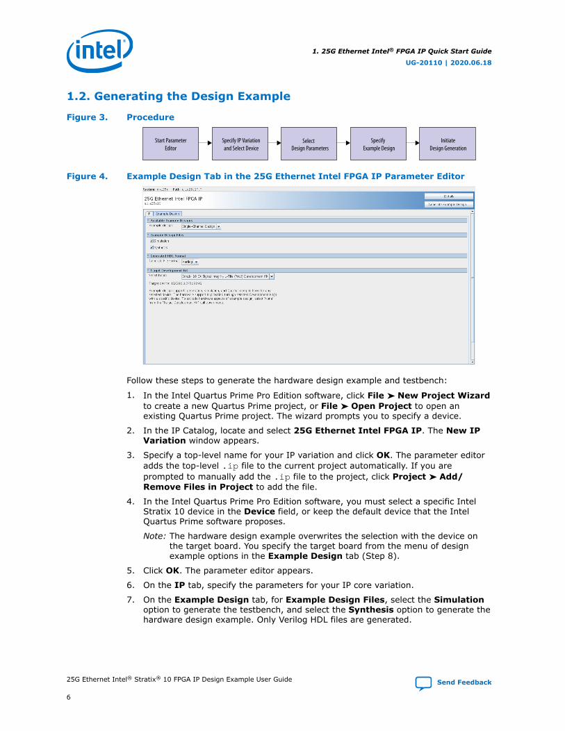
1.2. Generating the Design Example
Figure 3. Procedure
Start ParameterEditor
Specify IP Variationand Select Device
SelectDesign Parameters
InitiateDesign Generation
Specify Example Design
Figure 4. Example Design Tab in the 25G Ethernet Intel FPGA IP Parameter Editor
Follow these steps to generate the hardware design example and testbench:
1. In the Intel Quartus Prime Pro Edition software, click File ➤ New Project Wizardto create a new Quartus Prime project, or File ➤ Open Project to open anexisting Quartus Prime project. The wizard prompts you to specify a device.
2. In the IP Catalog, locate and select 25G Ethernet Intel FPGA IP. The New IPVariation window appears.
3. Specify a top-level name for your IP variation and click OK. The parameter editoradds the top-level .ip file to the current project automatically. If you areprompted to manually add the .ip file to the project, click Project ➤ Add/Remove Files in Project to add the file.
4. In the Intel Quartus Prime Pro Edition software, you must select a specific IntelStratix 10 device in the Device field, or keep the default device that the IntelQuartus Prime software proposes.
Note: The hardware design example overwrites the selection with the device onthe target board. You specify the target board from the menu of designexample options in the Example Design tab (Step 8).
5. Click OK. The parameter editor appears.
6. On the IP tab, specify the parameters for your IP core variation.
7. On the Example Design tab, for Example Design Files, select the Simulationoption to generate the testbench, and select the Synthesis option to generate thehardware design example. Only Verilog HDL files are generated.
1. 25G Ethernet Intel® FPGA IP Quick Start Guide
UG-20110 | 2020.06.18
25G Ethernet Intel® Stratix® 10 FPGA IP Design Example User Guide Send Feedback
6

Note: A functional VHDL IP core is not available. Specify Verilog HDL only, for yourIP core design example.
8. For Target Development Kit, select the Stratix 10 GX Signal Integrity L-Tile(Prod) Development Kit.
Note: The target device of the generated hardware example design is for IntelStratix 10 GX Signal Integrity L-Tile (Production) Development Kit(1SX280LU2F50E1VG) and may differ from your selected device. The targetdevice can be changed after hardware design example generation hascompleted. For the procedure to change the target device, refer to ChangingTarget Device in Hardware Design Example.
9. Click Generate Example Design. The Select Example Design Directorywindow appears.
10. If you want to modify the design example directory path or name from thedefaults displayed (alt_e25s10_0_example_design), browse to the new pathand type the new design example directory name (<design_example_dir>).
11. Click OK.
Related Information
Changing Target Device in Hardware Design Example on page 9
1.2.1. Design Example Parameters
Table 2. Parameters in the Example Design Tab
Parameter Description
Example Design Available example designs for the IP parameter settings.
Example Design Files The files to generate for the different development phase.• Simulation—generates the necessary files for simulating the example
design.• Synthesis—generates the synthesis files. Use these files to compile
the design in the Intel Quartus Prime Pro Edition software forhardware testing and perform static timing analysis.
Generate File Format The format of the RTL files for simulation—Verilog.
Select Board Supported hardware for design implementation. When you select anIntel FPGA development board, use device 1SX280LU2F50E1VG as theTarget Device for design example generation.If this menu is not available, there is no supported board for the optionsthat you select.Stratix 10 GX Signal Integrity L-Tile (Prod) Development Kit: Thisoption allows you to test the design example on the selected Intel FPGAIP development kit. This option automatically selects the Target Deviceof 1SX280LU2F50E1VG. If your board revision has a different devicegrade, you can change the target device.None: This option excludes the hardware aspects for the designexample.
1. 25G Ethernet Intel® FPGA IP Quick Start Guide
UG-20110 | 2020.06.18
Send Feedback 25G Ethernet Intel® Stratix® 10 FPGA IP Design Example User Guide
7
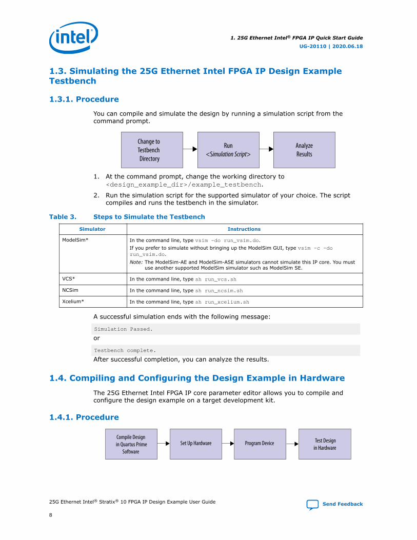
1.3. Simulating the 25G Ethernet Intel FPGA IP Design ExampleTestbench
1.3.1. Procedure
You can compile and simulate the design by running a simulation script from thecommand prompt.
Change to Testbench Directory
Run<Simulation Script>
AnalyzeResults
1. At the command prompt, change the working directory to<design_example_dir>/example_testbench.
2. Run the simulation script for the supported simulator of your choice. The scriptcompiles and runs the testbench in the simulator.
Table 3. Steps to Simulate the Testbench
Simulator Instructions
ModelSim* In the command line, type vsim -do run_vsim.do.If you prefer to simulate without bringing up the ModelSim GUI, type vsim -c -dorun_vsim.do.Note: The ModelSim-AE and ModelSim-ASE simulators cannot simulate this IP core. You must
use another supported ModelSim simulator such as ModelSim SE.
VCS* In the command line, type sh run_vcs.sh
NCSim In the command line, type sh run_ncsim.sh
Xcelium* In the command line, type sh run_xcelium.sh
A successful simulation ends with the following message:
Simulation Passed.
or
Testbench complete.
After successful completion, you can analyze the results.
1.4. Compiling and Configuring the Design Example in Hardware
The 25G Ethernet Intel FPGA IP core parameter editor allows you to compile andconfigure the design example on a target development kit.
1.4.1. Procedure
Compile Design in Quartus Prime
SoftwareSet Up Hardware Program Device Test Design
in Hardware
1. 25G Ethernet Intel® FPGA IP Quick Start Guide
UG-20110 | 2020.06.18
25G Ethernet Intel® Stratix® 10 FPGA IP Design Example User Guide Send Feedback
8

To compile and configure a design example on hardware, follow these steps:
1. Launch the Intel Quartus Prime Pro Edition software and select Processing ➤Start Compilation to compile the design.
2. After you generate an SRAM object file .sof, follow these steps to program thehardware design example on the Intel Stratix 10 device:
a. On the Tools menu, click Programmer.
b. In the Programmer, click Hardware Setup.
c. Select a programming device.
d. Select and add the Intel Stratix 10 GX board to your Intel Quartus Prime ProEdition session.
e. Ensure that Mode is set to JTAG.
f. Select the Intel Stratix 10 device and click Add Device. The Programmerdisplays a block diagram of the connections between the devices on yourboard.
g. In the row with your .sof, check the box for the .sof.
h. Check the box in the Program/Configure column.
i. Click Start.
Note: This design targets the Intel Stratix 10 device. Please contact your IntelFPGA representative to inquire about a platform suitable to run thishardware example.
Related Information
• Incremental Compilation for Hierarchical and Team-Based Design
• Programming Intel FPGA Devices
1.5. Changing Target Device in Hardware Design Example
If you have selected Intel Stratix 10 GX Signal Integrity L-Tile (Production)Development Kit as your target device, the 25G Ethernet Intel FPGA IP coregenerates a hardware example design for target device 1SX280LU2F50E1VG. Thisdevice may differ from the device on your development kit.
1.5.1. Procedure
To change the target device in your hardware design example, follow these steps:
1. Launch the Intel Quartus Prime Pro Edition software and open the hardware testproject file /hardware_test_design/eth_ex_25g.qpf.
2. On the Assignments menu, click Device. The Device dialog box appears.
3. In the Device dialog box, select 1SG280LU2F50E2VG (L-tile) or1SG280HU1F50E2VG (H-tile) in the target device table that matches the devicepart number on your development kit. Refer to the Stratix 10 GX Signal IntegrityDevelopment Kit link on the Intel website for more information.
4. A prompt appears when you select a device, as shown in the figure below. SelectNo to preserve the generated pin assignments and I/O assignments.
1. 25G Ethernet Intel® FPGA IP Quick Start Guide
UG-20110 | 2020.06.18
Send Feedback 25G Ethernet Intel® Stratix® 10 FPGA IP Design Example User Guide
9
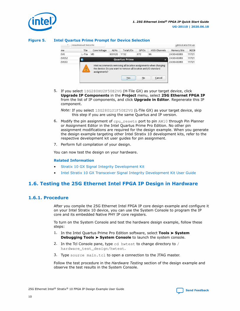
Figure 5. Intel Quartus Prime Prompt for Device Selection
5. If you select 1SG280HU2F50E2VG (H-Tile GX) as your target device, clickUpgrade IP Components in the Project menu, select 25G Ethernet FPGA IPfrom the list of IP components, and click Upgrade in Editor. Regenerate this IPcomponent.
Note: If you select 1SG280LU1F50E2VG (L-Tile GX) as your target device, skipthis step if you are using the same Quartus and IP version.
6. Modify the pin assignment of cpu_resetn port to pin AW10 through Pin Planneror Assignment Editor in the Intel Quartus Prime Pro Edition. No other pinassignment modifications are required for the design example. When you generatethe design example targeting other Intel Stratix 10 development kits, refer to therespective development kit user guides for pin assignment.
7. Perform full compilation of your design.
You can now test the design on your hardware.
Related Information
• Stratix 10 GX Signal Integrity Development Kit
• Intel Stratix 10 GX Transceiver Signal Integrity Development Kit User Guide
1.6. Testing the 25G Ethernet Intel FPGA IP Design in Hardware
1.6.1. Procedure
After you compile the 25G Ethernet Intel FPGA IP core design example and configure iton your Intel Stratix 10 device, you can use the System Console to program the IPcore and its embedded Native PHY IP core registers.
To turn on the System Console and test the hardware design example, follow thesesteps:
1. In the Intel Quartus Prime Pro Edition software, select Tools ➤ SystemDebugging Tools ➤ System Console to launch the system console.
2. In the Tcl Console pane, type cd hwtest to change directory to /hardware_test_design/hwtest.
3. Type source main.tcl to open a connection to the JTAG master.
Follow the test procedure in the Hardware Testing section of the design example andobserve the test results in the System Console.
1. 25G Ethernet Intel® FPGA IP Quick Start Guide
UG-20110 | 2020.06.18
25G Ethernet Intel® Stratix® 10 FPGA IP Design Example User Guide Send Feedback
10

Related Information
Analyzing and Debugging Designs with System Console
1. 25G Ethernet Intel® FPGA IP Quick Start Guide
UG-20110 | 2020.06.18
Send Feedback 25G Ethernet Intel® Stratix® 10 FPGA IP Design Example User Guide
11

2. 10G/25G Ethernet Single-Channel Design Example forIntel Stratix 10 Devices
The 10G/25G Ethernet single-channel design example demonstrates an Ethernetsolution for Intel Stratix 10 devices using the 25G Ethernet Intel FPGA IP core.
Generate the design example from the Example Design tab of the 25G Ethernet IntelFPGA IP parameter editor. You can choose to generate the design with or without theIEEE 1588v2 feature. You can also choose to generate the design with or without theReed-Solomon Forward Error Correction (RS-FEC) feature.
2.1. Features
• Supports single Ethernet channel operating at either 10G or 25G.
• Generate design example with IEEE 1588v2 feature.
• Generate design example with RS-FEC feature.
• Generates design example separately from Intel Stratix 10 Transceiver Native PHY.
• Provides testbench and simulation script.
2.2. Hardware and Software Requirements
Intel uses the following hardware and software to test the design example in a Linuxsystem:
• Intel Quartus Prime Pro Edition software.
• ModelSim-SE, NCSim (Verilog only), VCS, and Xcelium simulator.
• Intel Stratix 10 GX Signal Integrity L-Tile (Production) Development Kit(1SX280LU2F50E1VG) for hardware testing.
2.3. Functional Description
The 10G/25G Ethernet single-channel design example consists of two core variants—MAC+PCS+PMA and MAC+PCS. The following block diagrams show the designcomponents and the top-level signals of the two core variants in the 10G/25GEthernet single-channel design example.
UG-20110 | 2020.06.18
Send Feedback
Intel Corporation. All rights reserved. Agilex, Altera, Arria, Cyclone, Enpirion, Intel, the Intel logo, MAX, Nios,Quartus and Stratix words and logos are trademarks of Intel Corporation or its subsidiaries in the U.S. and/orother countries. Intel warrants performance of its FPGA and semiconductor products to current specifications inaccordance with Intel's standard warranty, but reserves the right to make changes to any products and servicesat any time without notice. Intel assumes no responsibility or liability arising out of the application or use of anyinformation, product, or service described herein except as expressly agreed to in writing by Intel. Intelcustomers are advised to obtain the latest version of device specifications before relying on any publishedinformation and before placing orders for products or services.*Other names and brands may be claimed as the property of others.
ISO9001:2015Registered
Figure 6. Block Diagram—10G/25G Ethernet Single-Channel Design Example (MAC+PCS+PMA Core Variant) Without the IEEE 1588v2 Feature
10G/25G Ethernet Single-Channel Design Example
AvalonMemory-Mapped
Fabric
25G Ethernet Intel FPGA IP(MAC+PCS+PMA)
Intel Stratix 10 GX Signal Integrity L-Tile (Production) Development Kit
tx_serial_clk(12.890625 GHz)
Avalon Streaming TX
Avalon Streaming RX
Loopback
Transceiver PHYMAC+PCSRS-FEC
(Optional)
Client Logic(Packet Generator
and Monitor)
Control and Status Interface
Intel Stratix 10 DynamicReconfiguration Interface
(5.15625 GHz)tx_serial_clk
SystemConsole
Reset(Full Design)
Multiplexer
Control and Status Interface
JTAGto
Avalon Memory-MappedBridge
Speed_selAvalon
Memory-Mapped
ATX PLL(25G)
ATX PLL(10G)
Source and ProbeSystem Reset(Full Design)
ReconfigurationSequencer
reconfig_switch
AvalonMemory-Mapped
AvalonMemory-Mapped
Figure 7. Block Diagram—10G/25G Ethernet Single-Channel Design Example (MAC+PCS+PMA Core Variant) with the IEEE 1588v2 Feature
10G/25G Ethernet Single-Channel Design Example
AvalonMemory-Mapped
Fabric
25G Ethernet Intel FPGA IP(MAC+PCS+PMA)
Intel Stratix 10 GX Signal Integrity L-Tile (Production) Development Kit
tx_serial_clk(12.890625 GHz)
Loopback
Transceiver PHYMAC+PCSRS-FEC
(optional)Master
PTP
Multipelxer
Demultiplexer
Rx Ingress TimeStamp Master[95:0]
Rx Data Master[63:0]
Rx Egress TimeStamp Master[95:0]
Rx Ingress TimeStamp Slave[95:0]
Rx Data Slave[63:0]
Rx Egress TimeStamp Slave[95:0]
Tx Data Slave[63:0]
Rx Ingress TimeStamp Master[95:0]
Avalon Streaming RX [63:0]
Tx Egress TimeStamp Master[95:0]
PTP Top Design Example
Avalon Streaming TX [63:0]
Average Offsetor Delay[31:0]
Tx data Master[63:0]
Avalon Memory-Mapped
ToD Tx(25G)
ToD Tx(10G)
SamplingPLL
ToD Rx(25G)
ToD Rx(10G)
ToD Sync(25G)
ToD Sync(10G)
100 Mhz333.33 Mhz
(5.15625 GHz)tx_serial_clk_10g
Multiplexer
SystemConsole
reconfig_switchSpeed_sel
tx_time_of_day_96b_datatx_time_of_day_64b_data
rx_time_of_day_96b_datarx_time_of_day_64b_data
ATX PLL(10G)
ATX PLL(25G)
Average Offsetor Delay[31:0]
Tx data Master[63:0]
Speed_sel
latency_sclk
SamplingPLLsampling_clk
System Reset(Full Design)
channel_reset
Multiplexer
Control and Status Interface
JTAG to AvalonMemory-Mapped
Bridge
Source and Probe
Multiplexer
SlavePTP
Intel Stratix 10Dynamic Reconfiguration
Interface
ReconfigurationSequencer
AvalonMemory-Mapped
Multiplexer
Avalon Memory-Mapped
AvalonMemory-Mapped
2. 10G/25G Ethernet Single-Channel Design Example for Intel Stratix 10 Devices
UG-20110 | 2020.06.18
Send Feedback 25G Ethernet Intel® Stratix® 10 FPGA IP Design Example User Guide
13

Figure 8. Block Diagram—10G/25G Ethernet Single-Channel Design Example (MAC+PCS Core Variant) Without the IEEE 1588v2 Feature
10G/25G Ethernet Single-Channel Design Example
25G Ethernet Intel FPGA IP(MAC+PCS)
Intel Stratix 10 GX Signal Integrity L-Tile (Production) Development Kit
tx_serial_clk(12.890625 GHz)
Avalon Streaming TX
Avalon Streaming RX
Loopback
MAC+PCS RS-FEC(optional)
Client Logic(Packet Generator
and Monitor)
Control and Status Interface
(5.15625 GHz)tx_serial_clk
Reset(Full Design)
Multiplexer
Control and Status Interface
Speed_sel
ATX PLL(25G)
ATX PLL(10G)
TX Control[1:0]
RX Control[1:0]
TX Parallel Data[63:0]
RX Parallel Data[63:0]
Note:1. Components outside of this block are part of the design example only.
(1)
Source and ProbeSystem Reset(Full Design)
reconfig_switch
AvalonMemory-Mapped
Fabric
SystemConsole
JTAGto
Avalon Memory-MappedBridge
AvalonMemory-Mapped
ReconfigurationSequencer
AvalonMemory-Mapped
Intel Stratix 10 DynamicReconfiguration Interface
Avalon Memory-Mapped
Transceiver PHY
Figure 9. Block Diagram—10G/25G Ethernet Single-Channel Design Example (MAC+PCS Core Variant) with the IEEE 1588v2 Feature
10G/25G Ethernet Single-Channel Design Example
System Reset(Full Design)
25G Ethernet Intel FPGA IP(MAC+PCS)
Intel Stratix 10 GX Signal Integrity L-Tile (Production) Development Kit
tx_serial_clk(12.890625 GHz)
LoopbackMAC+PCS
RS-FEC(Optional)Master
PTP
SlavePTP
Multipelxer
Demultiplexer
Rx Ingress TimeStamp Master[95:0]
Rx Data Master[63:0]
Rx Egress TimeStamp Master[95:0]
Rx Ingress TimeStamp Slave[95:0]
Rx Data Slave[63:0]
Rx Egress TimeStamp Slave[95:0]
Tx Data Slave[63:0]
Rx Ingress TimeStamp Master[95:0]
Avalon Streaming RX [63:0]
Tx Egress TimeStamp Master[95:0]
PTP Top Design Example
Avalon Streaming TX [63:0]
Tx data Master[63:0]
ToD Tx(25G)
ToD Tx(10G)
SamplingPLL
ToD Rx(25G)
ToD Rx(10G)
ToD Sync(25G)
ToD Sync(10G)
100 Mhz333.33 Mhz
Multiplexer
Multiplexer
(5.15625 GHz)tx_serial_clk
SystemConsole
reconfig_switch
Speed_sel
tx_time_of_day_96b_datatx_time_of_day_64b_data
rx_time_of_day_96b_datarx_time_of_day_64b_data
ATX PLL(10G)
ATX PLL(25G)
Average Offsetand Delay[47:0]
Tx data Master[63:0]
Speed_sel
latency_sclk
sampling_clk
(1)
Note:1. Components outside of this block are part of the design example only.
AvalonMemory-Mapped
Fabric
AvalonMemory- Mapped
Control and Status Interface
Average Offsetand Delay[47:0]
ReconfigurationSequencer
Multiplexer
Intel Stratix 10 DynamicReconfiguration Interface
AvalonMemory-Mapped
Reset(Full Design)
TransceiverPHY
TX Control[1:0]
RX Control[1:0]
TX Parallel Data[63:0]
RX Parallel Data[63:0]
Source and Probe
SamplingPLL
JTAG to AvalonMemory-Mapped
Bridge
AvalonMemory-Mapped
AvalonMemory- Mapped
2. 10G/25G Ethernet Single-Channel Design Example for Intel Stratix 10 Devices
UG-20110 | 2020.06.18
25G Ethernet Intel® Stratix® 10 FPGA IP Design Example User Guide Send Feedback
14

2.3.1. Design Components
Table 4. Design Components
Component Description
25G Ethernet Intel FPGA IP Consists of MAC, PCS, and Transceiver PHY, with the following configuration:• Core Variant: MAC+PCS+PMA, MAC+PCS• Enable flow control: Optional• Enable link fault generation: Optional• Enable preamble passthrough: Optional• Enable statistics collection: Optional• Enable MAC statistics counters: Optional• Enable 10G/25G dynamic rate switching: Selected• Enable Native PHY Debug Master Endpoint (NPDME): Optional• Reference clock frequency: 644.531250/322.265625For the design example with the IEEE 1588 feature, the following additional parameters areconfigured:• Enable IEEE 1588: Selected• Time of day format: Enable 96-bit timestamp format (1)
For the design example with the RS-FEC feature, the following additional parameter isconfigured:• Enable RS-FEC: Selected
Reconfiguration Sequencer Reconfigures the transceiver channel speed from 10 Gbps to 25 Gbps, and vice versa.
ATX PLL Generates TX serial clocks for the 10G and 25G transceivers.
Client logic Consists of:• Traffic generator, which generates burst packets to the 25G Ethernet Intel FPGA IP core
for transmission.• Traffic monitor, which receives burst packets from the 25G Ethernet Intel FPGA IP core.
Source and Probe Source and probe signals, including system reset input signal, which you can use fordebugging.
Design Components for the IEEE 1588v2 Feature
Sampling PLL Generates the clocks for the IEEE 1588v2 design components.• latency_sclk: 156.25 MHz for latency measurement.• sampling_clk: 250 MHz for ToD synchronization
Time-of-day (ToD) Sync Synchronizes the 10G and 25G ToDs.
ToD Tx ToD for transmit paths for the 10G and 25G transceivers.
ToD Rx ToD for receive paths for the 10G and 25G transceivers.
Master Precision TimeProtocol (PTP)
Master PTP consists of a packet generator and a packet receiver.• Packet generator: Obtains timestamp information from the 25G Ethernet Intel FPGA IP
core and generates Avalon® streaming packets such as Sync packet and DelayResponse packet.
• Packet receiver: Obtains the delay request packet information from the 25G EthernetIntel FPGA IP core and produces timestamp values.
Slave PTP Slave PTP consists of a packet generator, a packet receiver, and packet compute.continued...
(1) The 10G/25G Ethernet single-channel design example with IEEE 1588v2 feature only supports96-bit timestamp format.
2. 10G/25G Ethernet Single-Channel Design Example for Intel Stratix 10 Devices
UG-20110 | 2020.06.18
Send Feedback 25G Ethernet Intel® Stratix® 10 FPGA IP Design Example User Guide
15
Component Description
• Packet generator: Obtains timestamp information from the 25G Ethernet Intel FPGA IPcore and generates Avalon streaming packets such as Delay Request packet.
• Packet receiver: Obtains the Sync and Delay Response packets information from the25G Ethernet Intel FPGA IP core and produces timestamp values.
• Packet compute: Calculates and produces the delay and offsets value based on thetimestamp values.
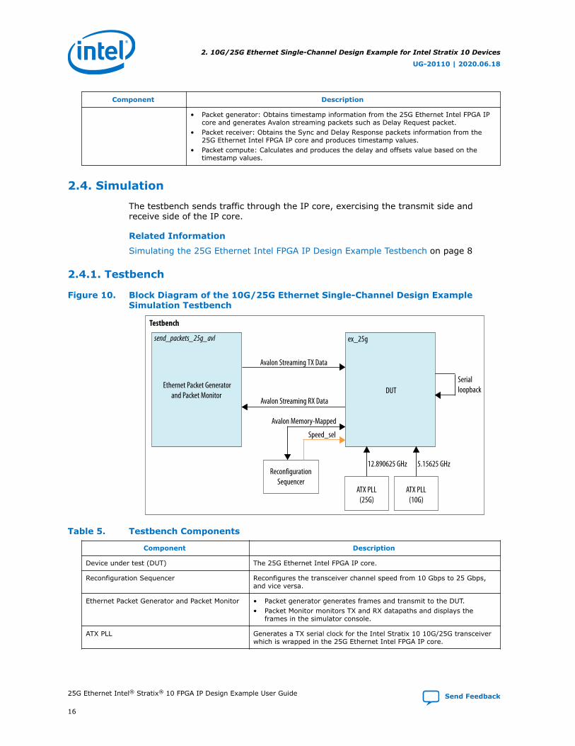
2.4. Simulation
The testbench sends traffic through the IP core, exercising the transmit side andreceive side of the IP core.
Related Information
Simulating the 25G Ethernet Intel FPGA IP Design Example Testbench on page 8
2.4.1. Testbench
Figure 10. Block Diagram of the 10G/25G Ethernet Single-Channel Design ExampleSimulation Testbench
Testbench
send_packets_25g_avl
Ethernet Packet Generatorand Packet Monitor
Avalon Streaming TX Data
Avalon Streaming RX Data
SerialloopbackDUT
ATX PLL(25G)
12.890625 GHz
ATX PLL(10G)
5.15625 GHz
ex_25g
ReconfigurationSequencer
Speed_sel
Avalon Memory-Mapped
Table 5. Testbench Components
Component Description
Device under test (DUT) The 25G Ethernet Intel FPGA IP core.
Reconfiguration Sequencer Reconfigures the transceiver channel speed from 10 Gbps to 25 Gbps,and vice versa.
Ethernet Packet Generator and Packet Monitor • Packet generator generates frames and transmit to the DUT.• Packet Monitor monitors TX and RX datapaths and displays the
frames in the simulator console.
ATX PLL Generates a TX serial clock for the Intel Stratix 10 10G/25G transceiverwhich is wrapped in the 25G Ethernet Intel FPGA IP core.
2. 10G/25G Ethernet Single-Channel Design Example for Intel Stratix 10 Devices
UG-20110 | 2020.06.18
25G Ethernet Intel® Stratix® 10 FPGA IP Design Example User Guide Send Feedback
16

Note: For the 10G/25G Ethernet single-channel design example with IEEE 1588v2 featuresimulation testbench, refer to Figure 7 on page 13.
2.4.2. Simulation Design Example Components
Table 6. 10G/25G Ethernet Single-Channel Design Example Testbench FileDescriptions
File Name Description
Testbench and Simulation Files
basic_avl_tb_top.sv Top-level testbench file. The testbench instantiates the DUT,performs Avalon memory-mapped configuration on designcomponents and client logic, and sends and receives packetto or from the 25G Ethernet Intel FPGA IP.
Testbench Scripts
run_vsim.do The ModelSim script to run the testbench.
run_vcs.sh The Synopsys VCS script to run the testbench.
run_ncsim.sh The Cadence NCSim script to run the testbench.
run_xcelium.sh The Xcelium script to run the testbench.
2.4.3. Test Case—Design Example Without the IEEE 1588v2 Feature
The simulation test case performs the following actions:
1. Instantiates 25G Ethernet Intel FPGA IP and ATX PLL.
2. Starts up the design example with an operating speed of 25G.
3. Waits for RX clock and PHY status signal to settle.
4. Prints PHY status.
5. Sends and receives 10 valid data on 25G speed.
6. Performs channel reset and switches to 10G speed.
7. Waits for RX clock and PHY status signal to settle.
8. Prints PHY status.
9. Sends and receives another 10 valid data on 10G speed.
10. Performs channel reset and switches to 25G speed.
11. Waits for RX clock and PHY status signal to settle.
12. Prints PHY status.
13. Sends and receives another 10 valid data on 25G speed.
14. Analyzes the results. The successful testbench displays "Simulation PASSED.".
The following sample output illustrates a successful simulation test run:
Waiting for RX alignmentRX deskew lockedRX lane alignmnet lockedTX enabled** Sending Packet 1...** Sending Packet 2...** Sending Packet 3...** Sending Packet 4...
2. 10G/25G Ethernet Single-Channel Design Example for Intel Stratix 10 Devices
UG-20110 | 2020.06.18
Send Feedback 25G Ethernet Intel® Stratix® 10 FPGA IP Design Example User Guide
17

** Sending Packet 5...** Sending Packet 6...** Sending Packet 7...** Sending Packet 8...** Received Packet 1...** Received Packet 2...** Sending Packet 9...** Sending Packet 10...** Received Packet 3...** Received Packet 4...** Received Packet 5...** Received Packet 7...** Received Packet 8...** Received Packet 9...** Received Packet 10...Switching to 10G mode: 10G Reconfig startSwitching to 10G mode: 10G Reconfig EndWaiting for RX alignmentRX deskew lockedRX lane alignment lockedTX enabled** Sending Packet 1...** Sending Packet 2...** Sending Packet 3...** Sending Packet 4...** Sending Packet 5...** Sending Packet 6...** Sending Packet 7...** Sending Packet 8...** Received Packet 1...** Received Packet 2...** Sending Packet 9...** Sending Packet 10...** Received Packet 3...** Received Packet 4...** Received Packet 5...** Received Packet 7...** Received Packet 8...** Received Packet 9...** Received Packet 10...Switching to 25G mode: 25G Reconfig startSwitching to 25G mode: 25G Reconfig EndWaiting for RX alignmentRX deskew lockedRX lane alignment lockedTX enabled** Sending Packet 1...** Sending Packet 2...** Sending Packet 3...** Sending Packet 4...** Sending Packet 5...** Sending Packet 6...** Sending Packet 7...** Sending Packet 8...** Received Packet 1...** Received Packet 2...** Sending Packet 9...** Sending Packet 10...** Received Packet 3...** Received Packet 4...** Received Packet 5...** Received Packet 7...** Received Packet 8...** Received Packet 9...** Received Packet 10...**** Testbench complete.**
2. 10G/25G Ethernet Single-Channel Design Example for Intel Stratix 10 Devices
UG-20110 | 2020.06.18
25G Ethernet Intel® Stratix® 10 FPGA IP Design Example User Guide Send Feedback
18

2.4.4. Test Case—Design Example with the IEEE 1588v2 Feature
Note: For 10G/25G Ethernet single-channel design example with IEEE 1588v2 featuresimulation testbench, refer to Figure 7 on page 13.
The simulation test case performs the following actions:
1. Instantiates 25G Ethernet Intel FPGA IP, ATX PLL, and IO PLL (sampling PLL).
2. Starts up the design example with an operating speed of 25G.
3. Waits for RX clock and PHY status signal to settle.
4. Prints PHY status.
5. Checks for 10 valid data on 25G speed.
6. Switches to 10G speed.
7. Waits for RX clock and PHY status signal to settle.
8. Prints PHY status.
9. Checks for another 10 valid data on 10G speed.
10. Switches to 25G speed once all 10 valid data passes.
11. Waits for RX clock and PHY status signal to settle.
12. Prints PHY status.
13. Checks for another 10 valid data on 25G speed.
14. Analyzes the results. The successful testbench displays "Simulation PASSED."when the PTP delay and offset data is within the threshold value.
The following sample output illustrates a successful simulation test run:
# Running at 25G mode...# # # Waiting for RX alignment...# iatpg_pipeline_global_en is set# iatpg_pipeline_global_en is set# RX deskew locked.# RX lane aligmnent locked.# # Sending packets...# # Delay (sec[95:48],ns[47:16],fns[15:0]): 0x000000000000000000064457# Offset(sec[95:48],ns[47:16],fns[15:0]): 0x000000000000000000000000# Offset within tolerence range.# # # Delay (sec[95:48],ns[47:16],fns[15:0]): 0x000000000000000000064bb4# Offset(sec[95:48],ns[47:16],fns[15:0]): 0x000000000000fffffffff8a2# Offset within tolerence range.# # # Delay (sec[95:48],ns[47:16],fns[15:0]): 0x0000000000000000000643b5# Offset(sec[95:48],ns[47:16],fns[15:0]): 0x000000000000000000000520# Offset within tolerence range.# # # Delay (sec[95:48],ns[47:16],fns[15:0]): 0x0000000000000000000634fb# Offset(sec[95:48],ns[47:16],fns[15:0]): 0x000000000000000000000000# Offset within tolerence range.# # # Delay (sec[95:48],ns[47:16],fns[15:0]): 0x000000000000000000063f3b
2. 10G/25G Ethernet Single-Channel Design Example for Intel Stratix 10 Devices
UG-20110 | 2020.06.18
Send Feedback 25G Ethernet Intel® Stratix® 10 FPGA IP Design Example User Guide
19
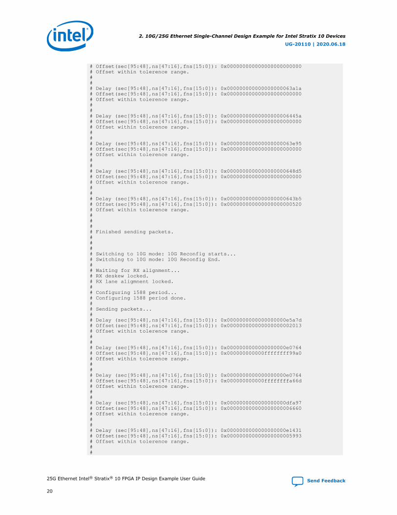
# Offset(sec[95:48],ns[47:16],fns[15:0]): 0x000000000000000000000000# Offset within tolerence range.# # # Delay (sec[95:48],ns[47:16],fns[15:0]): 0x000000000000000000063a1a# Offset(sec[95:48],ns[47:16],fns[15:0]): 0x000000000000000000000000# Offset within tolerence range.# # # Delay (sec[95:48],ns[47:16],fns[15:0]): 0x00000000000000000006445a# Offset(sec[95:48],ns[47:16],fns[15:0]): 0x000000000000000000000000# Offset within tolerence range.# # # Delay (sec[95:48],ns[47:16],fns[15:0]): 0x000000000000000000063e95# Offset(sec[95:48],ns[47:16],fns[15:0]): 0x000000000000000000000000# Offset within tolerence range.# # # Delay (sec[95:48],ns[47:16],fns[15:0]): 0x0000000000000000000648d5# Offset(sec[95:48],ns[47:16],fns[15:0]): 0x000000000000000000000000# Offset within tolerence range.# # # Delay (sec[95:48],ns[47:16],fns[15:0]): 0x0000000000000000000643b5# Offset(sec[95:48],ns[47:16],fns[15:0]): 0x000000000000000000000520# Offset within tolerence range.# # # # Finished sending packets.# # # # Switching to 10G mode: 10G Reconfig starts...# Switching to 10G mode: 10G Reconfig End.# # Waiting for RX alignment...# RX deskew locked.# RX lane aligmnent locked.# # Configuring 1588 period...# Configuring 1588 period done.# # Sending packets...# # Delay (sec[95:48],ns[47:16],fns[15:0]): 0x0000000000000000000e5a7d# Offset(sec[95:48],ns[47:16],fns[15:0]): 0x000000000000000000002013# Offset within tolerence range.# # # Delay (sec[95:48],ns[47:16],fns[15:0]): 0x0000000000000000000e0764# Offset(sec[95:48],ns[47:16],fns[15:0]): 0x000000000000ffffffff99a0# Offset within tolerence range.# # # Delay (sec[95:48],ns[47:16],fns[15:0]): 0x0000000000000000000e0764# Offset(sec[95:48],ns[47:16],fns[15:0]): 0x000000000000ffffffffa66d# Offset within tolerence range.# # # Delay (sec[95:48],ns[47:16],fns[15:0]): 0x0000000000000000000dfa97# Offset(sec[95:48],ns[47:16],fns[15:0]): 0x000000000000000000006660# Offset within tolerence range.# # # Delay (sec[95:48],ns[47:16],fns[15:0]): 0x0000000000000000000e1431# Offset(sec[95:48],ns[47:16],fns[15:0]): 0x000000000000000000005993# Offset within tolerence range.# #
2. 10G/25G Ethernet Single-Channel Design Example for Intel Stratix 10 Devices
UG-20110 | 2020.06.18
25G Ethernet Intel® Stratix® 10 FPGA IP Design Example User Guide Send Feedback
20
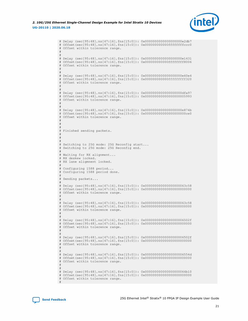
# Delay (sec[95:48],ns[47:16],fns[15:0]): 0x0000000000000000000e2db7# Offset(sec[95:48],ns[47:16],fns[15:0]): 0x000000000000ffffffffccc0# Offset within tolerence range.# # # Delay (sec[95:48],ns[47:16],fns[15:0]): 0x0000000000000000000e1431# Offset(sec[95:48],ns[47:16],fns[15:0]): 0x000000000000ffffffff8006# Offset within tolerence range.# # # Delay (sec[95:48],ns[47:16],fns[15:0]): 0x0000000000000000000e60e4# Offset(sec[95:48],ns[47:16],fns[15:0]): 0x000000000000fffffffff320# Offset within tolerence range.# # # Delay (sec[95:48],ns[47:16],fns[15:0]): 0x0000000000000000000dfa97# Offset(sec[95:48],ns[47:16],fns[15:0]): 0x000000000000000000005993# Offset within tolerence range.# # # Delay (sec[95:48],ns[47:16],fns[15:0]): 0x0000000000000000000e874b# Offset(sec[95:48],ns[47:16],fns[15:0]): 0x000000000000000000000ce0# Offset within tolerence range.# # # # Finished sending packets.# # # # Switching to 25G mode: 25G Reconfig start...# Switching to 25G mode: 25G Reconfig end.# # Waiting for RX alignment...# RX deskew locked.# RX lane aligmnent locked.# # Configuring 1588 period...# Configuring 1588 period done.# # Sending packets...# # Delay (sec[95:48],ns[47:16],fns[15:0]): 0x000000000000000000063c58# Offset(sec[95:48],ns[47:16],fns[15:0]): 0x000000000000000000000000# Offset within tolerence range.# # # Delay (sec[95:48],ns[47:16],fns[15:0]): 0x000000000000000000063c58# Offset(sec[95:48],ns[47:16],fns[15:0]): 0x000000000000000000000000# Offset within tolerence range.# # # Delay (sec[95:48],ns[47:16],fns[15:0]): 0x00000000000000000006502f# Offset(sec[95:48],ns[47:16],fns[15:0]): 0x000000000000000000000000# Offset within tolerence range.# # # Delay (sec[95:48],ns[47:16],fns[15:0]): 0x00000000000000000006502f# Offset(sec[95:48],ns[47:16],fns[15:0]): 0x000000000000000000000000# Offset within tolerence range.# # # Delay (sec[95:48],ns[47:16],fns[15:0]): 0x00000000000000000006554d# Offset(sec[95:48],ns[47:16],fns[15:0]): 0x000000000000000000000000# Offset within tolerence range.# # # Delay (sec[95:48],ns[47:16],fns[15:0]): 0x000000000000000000064b10# Offset(sec[95:48],ns[47:16],fns[15:0]): 0x000000000000000000000000# Offset within tolerence range.#
2. 10G/25G Ethernet Single-Channel Design Example for Intel Stratix 10 Devices
UG-20110 | 2020.06.18
Send Feedback 25G Ethernet Intel® Stratix® 10 FPGA IP Design Example User Guide
21

# # Delay (sec[95:48],ns[47:16],fns[15:0]): 0x000000000000000000064b10# Offset(sec[95:48],ns[47:16],fns[15:0]): 0x000000000000000000000000# Offset within tolerence range.# # # Delay (sec[95:48],ns[47:16],fns[15:0]): 0x000000000000000000064bb4# Offset(sec[95:48],ns[47:16],fns[15:0]): 0x000000000000000000000000# Offset within tolerence range.# # # Delay (sec[95:48],ns[47:16],fns[15:0]): 0x000000000000000000064bb4# Offset(sec[95:48],ns[47:16],fns[15:0]): 0x000000000000000000000000# Offset within tolerence range.# # # Delay (sec[95:48],ns[47:16],fns[15:0]): 0x000000000000000000065a6c# Offset(sec[95:48],ns[47:16],fns[15:0]): 0x000000000000000000000000# Offset within tolerence range.# # # # Finished sending packets.# # **# ** Testbench complete.# **
2.5. Compilation
Follow the procedure in Compiling and Configuring the Design Example in Hardware onpage 8 to compile and configure the design example in the selected hardware.
You can estimate resource utilization and Fmax using the compilation-only designexample. You can compile your design using the Start Compilation command on theProcessing menu in the Intel Quartus Prime Pro Edition software. A successfulcompilation generates the compilation report summary.
For more information, refer to Design Compilation in the Compiler User Guide: IntelQuartus Prime Pro Edition.
Related Information
Design CompilationIn Compiler User Guide: Intel Quartus Prime Pro Edition
2.6. Hardware Testing
In the hardware design example, you can program the IP core in internal serialloopback mode and generate traffic on the transmit side that loops back through thereceive side.
Follow the procedure at the provided related information link to test the designexample in the selected hardware.
Related Information
Testing the 25G Ethernet Intel FPGA IP Design in Hardware on page 10More information on the procedure and hardware setup.
2. 10G/25G Ethernet Single-Channel Design Example for Intel Stratix 10 Devices
UG-20110 | 2020.06.18
25G Ethernet Intel® Stratix® 10 FPGA IP Design Example User Guide Send Feedback
22
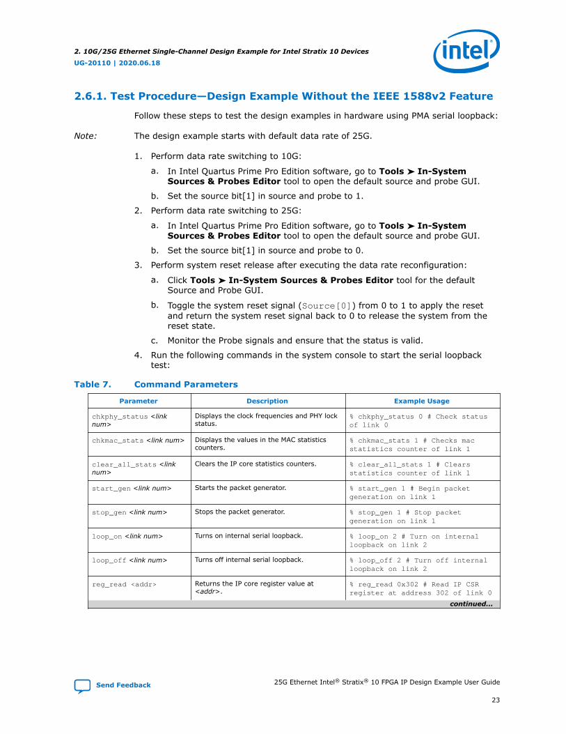
2.6.1. Test Procedure—Design Example Without the IEEE 1588v2 Feature
Follow these steps to test the design examples in hardware using PMA serial loopback:
Note: The design example starts with default data rate of 25G.
1. Perform data rate switching to 10G:
a. In Intel Quartus Prime Pro Edition software, go to Tools ➤ In-SystemSources & Probes Editor tool to open the default source and probe GUI.
b. Set the source bit[1] in source and probe to 1.
2. Perform data rate switching to 25G:
a. In Intel Quartus Prime Pro Edition software, go to Tools ➤ In-SystemSources & Probes Editor tool to open the default source and probe GUI.
b. Set the source bit[1] in source and probe to 0.
3. Perform system reset release after executing the data rate reconfiguration:
a. Click Tools ➤ In-System Sources & Probes Editor tool for the defaultSource and Probe GUI.
b. Toggle the system reset signal (Source[0]) from 0 to 1 to apply the resetand return the system reset signal back to 0 to release the system from thereset state.
c. Monitor the Probe signals and ensure that the status is valid.
4. Run the following commands in the system console to start the serial loopbacktest:
Table 7. Command Parameters
Parameter Description Example Usage
chkphy_status <linknum>
Displays the clock frequencies and PHY lockstatus.
% chkphy_status 0 # Check statusof link 0
chkmac_stats <link num> Displays the values in the MAC statisticscounters.
% chkmac_stats 1 # Checks macstatistics counter of link 1
clear_all_stats <linknum>
Clears the IP core statistics counters. % clear_all_stats 1 # Clearsstatistics counter of link 1
start_gen <link num> Starts the packet generator. % start_gen 1 # Begin packetgeneration on link 1
stop_gen <link num> Stops the packet generator. % stop_gen 1 # Stop packetgeneration on link 1
loop_on <link num> Turns on internal serial loopback. % loop_on 2 # Turn on internalloopback on link 2
loop_off <link num> Turns off internal serial loopback. % loop_off 2 # Turn off internalloopback on link 2
reg_read <addr> Returns the IP core register value at<addr>.
% reg_read 0x302 # Read IP CSRregister at address 302 of link 0
continued...
2. 10G/25G Ethernet Single-Channel Design Example for Intel Stratix 10 Devices
UG-20110 | 2020.06.18
Send Feedback 25G Ethernet Intel® Stratix® 10 FPGA IP Design Example User Guide
23
Parameter Description Example Usage
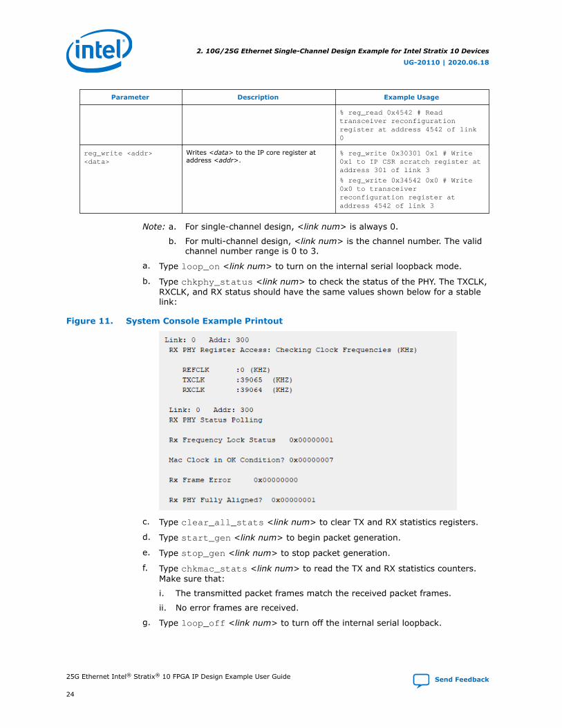
% reg_read 0x4542 # Readtransceiver reconfigurationregister at address 4542 of link0
reg_write <addr><data>
Writes <data> to the IP core register ataddress <addr>.
% reg_write 0x30301 0x1 # Write0x1 to IP CSR scratch register ataddress 301 of link 3
% reg_write 0x34542 0x0 # Write0x0 to transceiverreconfiguration register ataddress 4542 of link 3
Note: a. For single-channel design, <link num> is always 0.
b. For multi-channel design, <link num> is the channel number. The validchannel number range is 0 to 3.
a. Type loop_on <link num> to turn on the internal serial loopback mode.
b. Type chkphy_status <link num> to check the status of the PHY. The TXCLK,RXCLK, and RX status should have the same values shown below for a stablelink:
Figure 11. System Console Example Printout
c. Type clear_all_stats <link num> to clear TX and RX statistics registers.
d. Type start_gen <link num> to begin packet generation.
e. Type stop_gen <link num> to stop packet generation.
f. Type chkmac_stats <link num> to read the TX and RX statistics counters.Make sure that:
i. The transmitted packet frames match the received packet frames.
ii. No error frames are received.
g. Type loop_off <link num> to turn off the internal serial loopback.
2. 10G/25G Ethernet Single-Channel Design Example for Intel Stratix 10 Devices
UG-20110 | 2020.06.18
25G Ethernet Intel® Stratix® 10 FPGA IP Design Example User Guide Send Feedback
24
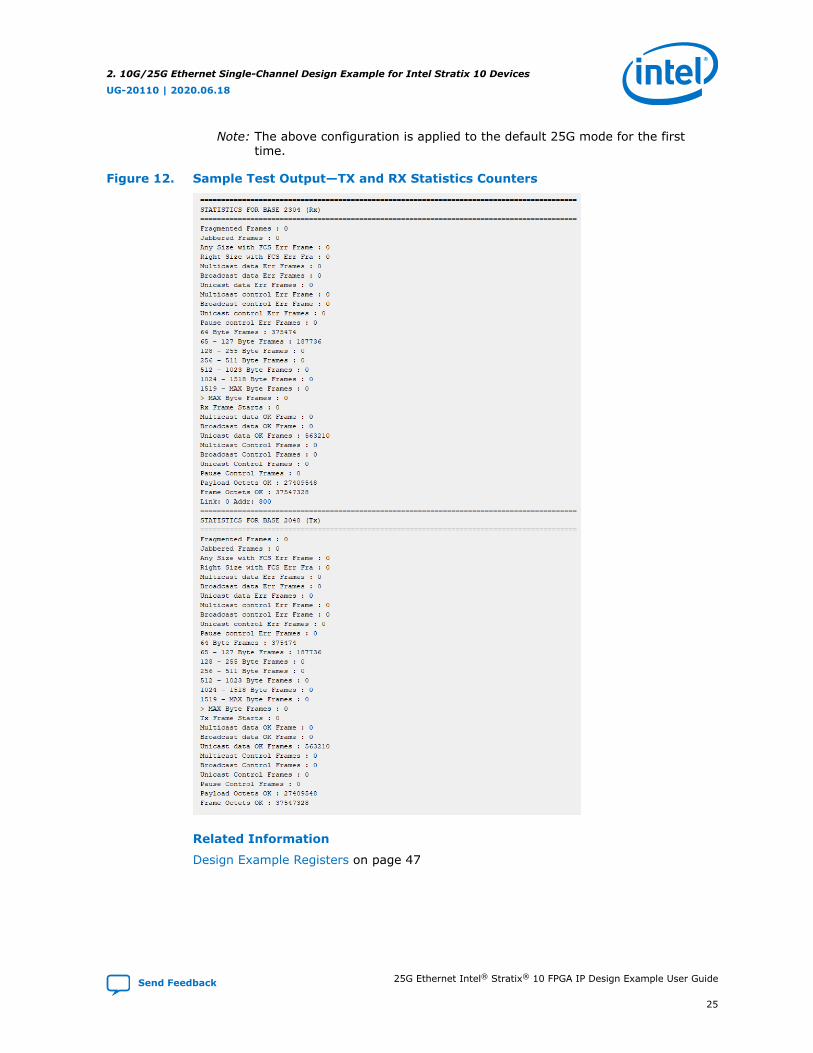
Note: The above configuration is applied to the default 25G mode for the firsttime.
Figure 12. Sample Test Output—TX and RX Statistics Counters
Related Information
Design Example Registers on page 47
2. 10G/25G Ethernet Single-Channel Design Example for Intel Stratix 10 Devices
UG-20110 | 2020.06.18
Send Feedback 25G Ethernet Intel® Stratix® 10 FPGA IP Design Example User Guide
25

2.6.2. Test Procedure—Design Example with the IEEE 1588v2 Feature
Follow these steps to test the design examples in hardware using PMA serial loopback:
Note: The design example starts with default data rate of 25G.
1. Perform data rate switching to 10G:
a. In Intel Quartus Prime Pro Edition software, go to Tools ➤ In-SystemSources & Probes Editor tool to open the default source and probe GUI.
b. Set the source bit[1] in source and probe to 1.
c. In the System Console panel, type the following commands as below to setthe correct clock period for the required TX and RX MAC clock frequency in10G speed mode:
reg_write 0xA05 0x66666reg_write 0xB05 0x66666
2. Perform data rate switching to 25G:
a. In Intel Quartus Prime Pro Edition software, go to Tools ➤ In-SystemSources & Probes Editor tool to open the default source and probe GUI.
b. Set the source bit[1] in source and probe to 0.
c. In the System Console panel, type the following commands as below to setthe correct clock period for the required TX and RX MAC clock frequency in25G speed mode:
reg_write 0xA05 0x28F5Creg_write 0xB05 0x28F5C
Note: 0xA05 is register that configure TX_PTP_CLK_PERIOD. 0xB05 is registerthat configure RX_PTP_CLK_PERIOD.
3. Perform system reset release after executing the data rate reconfiguration:
a. Click Tools ➤ In-System Sources & Probes Editor tool for the defaultSource and Probe GUI.
b. Toggle the system reset signal (Source[0]) from 0 to 1 to apply the resetand return the system reset signal back to 0 to release the system from thereset state.
c. Monitor the Probe signals and ensure that the status is valid.
4. To perform internal serial loopback test, refer to the Test Procedure—DesignExample Without the IEEE 1588v2 Feature section of this chapter.
Related Information
• Design Example Registers on page 47
• Test Procedure—Design Example Without the IEEE 1588v2 Feature on page 23
2. 10G/25G Ethernet Single-Channel Design Example for Intel Stratix 10 Devices
UG-20110 | 2020.06.18
25G Ethernet Intel® Stratix® 10 FPGA IP Design Example User Guide Send Feedback
26

3. 25G Ethernet Single-Channel Design Example for IntelStratix 10 Devices
The 25G Ethernet single-channel design example demonstrates an Ethernet solutionfor Intel Stratix 10 devices using the 25G Ethernet Intel FPGA IP core.
Generate the design example from the Example Design tab of the 25G Ethernet IntelFPGA IP parameter editor. You can choose to generate the design with or without theIEEE 1588v2 feature. You can also choose to generate the design with or without theReed-Solomon Forward Error Correction (RS-FEC) feature.
3.1. Features
• Supports single Ethernet channel operating at 25G.
• Generates design example with IEEE 1588v2 feature.
• Generates design example with RS-FEC feature.
• Generates design example separately from Intel Stratix 10 Transceiver Native PHY.
• Provides testbench and simulation script.
3.2. Hardware and Software Requirements
Intel uses the following hardware and software to test the design example in a Linuxsystem:
• Intel Quartus Prime Pro Edition software.
• ModelSim-SE, NCSim (Verilog only), VCS, and Xcelium simulator.
• Intel Stratix 10 GX Signal Integrity L-Tile (Production) Development Kit(1SX280LU2F50E1VG) for hardware testing.
3.3. Functional Description
The 25G Ethernet single-channel design example consists of two core variants—MAC+PCS+PMA and MAC+PCS. The following block diagrams show the design componentsand the top-level signals of the two core variants in the 25G Ethernet single-channeldesign example.
UG-20110 | 2020.06.18
Send Feedback
Intel Corporation. All rights reserved. Agilex, Altera, Arria, Cyclone, Enpirion, Intel, the Intel logo, MAX, Nios,Quartus and Stratix words and logos are trademarks of Intel Corporation or its subsidiaries in the U.S. and/orother countries. Intel warrants performance of its FPGA and semiconductor products to current specifications inaccordance with Intel's standard warranty, but reserves the right to make changes to any products and servicesat any time without notice. Intel assumes no responsibility or liability arising out of the application or use of anyinformation, product, or service described herein except as expressly agreed to in writing by Intel. Intelcustomers are advised to obtain the latest version of device specifications before relying on any publishedinformation and before placing orders for products or services.*Other names and brands may be claimed as the property of others.
ISO9001:2015Registered

Figure 13. Block Diagram—25G Ethernet Single-Channel Design Example (MAC+PCS+PMA Core Variant) Without the IEEE 1588v2 Feature
25G Ethernet Single-Channel Design Example(MAC+PCS+PMA)
System Reset(Full Design)
25G Ethernet Intel FPGA IP(MAC+PCS+PMA)
Intel Stratix 10 GX Signal Integrity L-Tile (Production) Development Kit
AvalonMemory-Mapped
Avalon Streaming TX
Avalon Streaming RX
Loopback
Control and Status Interface
Transceiver PHYMAC+PCSRS-FEC
(Optional)
Client Logic(Packet Generator
and Monitor)
Control and Status Interface
Intel Stratix 10 DynamicReconfiguration Interface
tx_serial_clk(12.890625 GHz)
ATX PLL(25G)
Source and Probe
AvalonMemory-Mapped
Fabric
SystemConsole
JTAGto
Avalon Memory-MappedBridge
Avalon Memory-Mapped
Figure 14. Block Diagram—25G Ethernet Single-Channel Design Example (MAC+PCS+PMA Core Variant) with the IEEE 1588v2 Feature
25G Ethernet Single-Channel Design Example
25G Ethernet Intel FPGA IP(MAC+PCS+PMA)
Intel Stratix 10 GX Signal Integrity L-Tile (Production) Development Kit
Avalon Memory-Mapped
tx_serial_clk(12.890625 GHz)
Loopback
Transceiver PHYMAC+PCSRS-FEC
(Optional)
JTAG toAvalon
Memory-MappedBridgeIntel Stratix 10 Dynamic
Reconfiguration Interface
MasterPTP
SlavePTP
Multipelxer
Demultiplexer
ToD Tx(25G)
SamplingPLL
ToD Rx(25G)ToD Sync
Rx Ingress TimeStamp Master[95:0]
Rx Data Master[63:0]
Rx Egress TimeStamp Master[95:0]
Rx Ingress TimeStamp Slave[95:0]
Rx Data Slave[63:0]
Rx Egress TimeStamp Slave[95:0]
Tx Data Slave[63:0]
100 Mhz333.33 Mhz
Rx Ingress TimeStamp Master[95:0]
Avalon Streaming RX [63:0]
Tx Egress TimeStamp Master[95:0]
PTP Top Design Example
Average Offsetand Delay[47:0]
Tx data Master[63:0]
Avalon Streaming TX [63:0]
tx_time_of_day_96b_datatx_time_of_day_64b_data rx_time_of_day_96b_data
rx_time_of_day_64b_data
SystemConsole
AvalonMemory-Mapped
Fabric
ATX PLL(25G)
Control and Status Interface
Tx data Master[63:0]
Average Offsetand Delay[47:0]
SamplingPLL
latency_sclk
sampling_clk
System Reset(Full Design)
Source and Probe
3. 25G Ethernet Single-Channel Design Example for Intel Stratix 10 Devices
UG-20110 | 2020.06.18
25G Ethernet Intel® Stratix® 10 FPGA IP Design Example User Guide Send Feedback
28

Figure 15. Block Diagram—25G Ethernet Single-Channel Design Example (MAC+PCSCore Variant) Without the IEEE 1588v2 Feature
25G Ethernet Single-Channel Design Example
25G Ethernet Intel FPGA IP(MAC+PCS)
Intel Stratix 10 GX Signal Integrity L-Tile (Production) Development Kit
Avalon Streaming TX
Avalon Streaming RX
Loopback
Control and Status Interface
Transceiver PHYMAC+PCS RS-FEC(Optional)
Client Logic(Packet Generator
and Monitor)and
Control and StatusInterface
Control Logic
Intel Stratix 10 DynamicReconfiguration Interface
SystemConsole
tx_serial_clk(12.890625 GHz)
TX Control[1:0]
System Reset(Full Design)
Source and Probe
pll_locked
ATX PLL(25G)
(1)
Note:1. Components outside of this block are part of the design example only.
RX Control[1:0]
TX Parallel Data[63:0]
RX Parallel Data[63:0]
Avalon Memory-Mapped
JTAGto
Avalon Memory-MappedBridge
AvalonMemory-Mapped
Fabric
Avalon Memory-Mapped
Figure 16. Block Diagram—25G Ethernet Single-Channel Design Example (MAC+PCSCore Variant) with the IEEE 1588v2 Feature
25G Ethernet Single-Channel Design Example
Source and ProbeSystem Reset(Full Design)
25G Ethernet Intel FPGA IP(MAC+PCS)
Intel Stratix 10 GX Signal Integrity L-Tile (Production) Development Kit
tx_serial_clk(12.890625 GHz)
Loopback
Transceiver PHYMAC+PCSRS-FEC
(Optional)
Intel Stratix 10 DynamicReconfiguration Interface
MasterPTP
SlavePTP
Multipelxer
Demultiplexer
ToD Tx(25G)
SamplingPLL
ToD Rx(25G)ToD Sync
Rx Ingress TimeStamp Master[95:0]
Rx Data Master[63:0]
Rx Egress TimeStamp Master[95:0]
Rx Ingress TimeStamp Slave[95:0]
Rx Data Slave[63:0]
Rx Egress TimeStamp Slave[95:0]
Tx Data Slave[63:0]
100 Mhz333.33 Mhz
Rx Ingress TimeStamp Master[95:0]
Avalon Streaming RX [63:0]
Tx Egress TimeStamp Master[95:0]
PTP Top Design Example
Average Offsetand Delay[47:0]
Tx data Master[63:0]
Avalon Streaming TX [63:0]
tx_time_of_day_96b_datatx_time_of_day_64b_data rx_time_of_day_96b_data
rx_time_of_day_64b_data
SystemConsole
ATX PLL(25G)
Control and Status Interface
Tx data Master[63:0]
Average Offsetand Delay[47:0]
SamplingPLL
latency_sclk
sampling_clk
(1)
Note:1. Components outside of this block are part of the design example only.
TX Control[1:0]
RX Control[1:0]
TX Parallel Data[63:0]
RX Parallel Data[63:0]
AvalonMemory-Mapped
Fabric
JTAGto
Avalon Memory-MappedBridge
3. 25G Ethernet Single-Channel Design Example for Intel Stratix 10 Devices
UG-20110 | 2020.06.18
Send Feedback 25G Ethernet Intel® Stratix® 10 FPGA IP Design Example User Guide
29

3.3.1. Design Components
Table 8. Design Components
Component Description
25G Ethernet Intel FPGA IP Consists of MAC, PCS, and Transceiver PHY, with the following configuration:• Core Variant: MAC+PCS+PMA, MAC+PCS• Enable flow control: Optional• Enable link fault generation: Optional• Enable preamble passthrough: Optional• Enable statistics collection: Optional• Enable MAC statistics counters: Optional• Enable 10G/25G dynamic rate switching: Not selected• Enable Native PHY Debug Master Endpoint (NPDME): Optional• Reference clock frequency: 644.531250/322.265625For the design example with the IEEE 1588 feature, the following additional parameters areconfigured:• Enable IEEE 1588: Selected• Time of day format: Enable 96-bit timestamp format (2)
For the design example with the RS-FEC feature, the following additional parameter isconfigured:• Enable RS-FEC: Selected
ATX PLL Generates TX serial clocks for the 25G transceiver.
Client logic Consists of:• Traffic generator, which generates burst packets to the 25G Ethernet Intel FPGA IP core
for transmission.• Traffic monitor, which monitors burst packets that are coming from the 25G Ethernet
Intel FPGA IP core.
Source and Probe Source and probe signals, including system reset input signal, which you can use fordebugging.
Design Components for the IEEE 1588v2 Feature
Sampling PLL Generates the clocks for the IEEE 1588v2 design components.• latency_sclk: 156.25 MHz for latency measurement.• sampling_clk: 250 MHz for ToD synchronization
Time-of-day (ToD) Sync Synchronizes the 25G ToD.
ToD Tx ToD for transmit paths for the 25G transceiver.
ToD Rx ToD for receive paths for the 25G transceiver.
Master Precision TimeProtocol (PTP)
Master PTP consists of a packet generator and a packet receiver.• Packet generator: Obtains timestamp information from the 25G Ethernet Intel FPGA IP
core and generates Avalon streaming packets such as Sync packet and Delay Responsepacket.
• Packet receiver: Obtains the delay request packet information from the 25G EthernetIntel FPGA IP core and produces timestamp values.
Slave PTP Slave PTP consists of a packet generator, a packet receiver, and a packet compute.continued...
(2) The 25G Ethernet single-channel design example with IEEE 1588v2 feature only supports 96-bit timestamp format.
3. 25G Ethernet Single-Channel Design Example for Intel Stratix 10 Devices
UG-20110 | 2020.06.18
25G Ethernet Intel® Stratix® 10 FPGA IP Design Example User Guide Send Feedback
30
Component Description
• Packet generator: Obtains timestamp information from the 25G Ethernet Intel FPGA IPcore and generates Avalon streaming packets such as Delay Request packet.
• Packet receiver: Obtains the Sync and Delay Response packets information from the25G Ethernet Intel FPGA IP core and produces timestamp values.
• Packet compute: Calculates and produces the delay and offsets value based on thetimestamp values.
3.4. Simulation
The testbench sends traffic through the IP core, exercising the transmit side andreceive side of the IP core.
Related Information
Simulating the 25G Ethernet Intel FPGA IP Design Example Testbench on page 8
3.4.1. Testbench
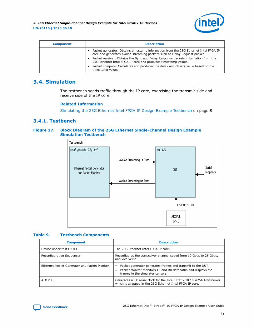
Figure 17. Block Diagram of the 25G Ethernet Single-Channel Design ExampleSimulation Testbench
Testbench
send_packets_25g_avl
Avalon Streaming TX Data
Avalon Streaming RX Data
Serialloopback
DUT
ATX PLL(25G)
12.890625 GHz
Ethernet Packet Generatorand Packet Monitor
ex_25g
Table 9. Testbench Components
Component Description
Device under test (DUT) The 25G Ethernet Intel FPGA IP core.
Reconfiguration Sequencer Reconfigures the transceiver channel speed from 10 Gbps to 25 Gbps,and vice versa.
Ethernet Packet Generator and Packet Monitor • Packet generator generates frames and transmit to the DUT.• Packet Monitor monitors TX and RX datapaths and displays the
frames in the simulator console.
ATX PLL Generates a TX serial clock for the Intel Stratix 10 10G/25G transceiverwhich is wrapped in the 25G Ethernet Intel FPGA IP core.
3. 25G Ethernet Single-Channel Design Example for Intel Stratix 10 Devices
UG-20110 | 2020.06.18
Send Feedback 25G Ethernet Intel® Stratix® 10 FPGA IP Design Example User Guide
31

Note: For the 25G Ethernet single-channel design example with IEEE 1588v2 featuresimulation testbench, refer to Figure 14 on page 28.
3.4.2. Simulation Design Example Components
Table 10. 25G Ethernet Single-Channel Design Example Testbench File Descriptions
File Name Description
Testbench and Simulation Files
basic_avl_tb_top.v Top-level testbench file. The testbench instantiates the DUT,performs Avalon memory-mapped configuration on designcomponents and client logic, and sends and receives packetto or from the 25G Ethernet Intel FPGA IP.
Testbench Scripts
run_vsim.do The ModelSim script to run the testbench.
run_vcs.sh The Synopsys VCS script to run the testbench.
run_ncsim.sh The Cadence NCSim script to run the testbench.
run_xcelium.sh The Xcelium script to run the testbench.
3.4.3. Test Case—Design Example Without the IEEE 1588v2 Feature
The simulation test case performs the following actions:
1. Instantiates and ATX PLL.
2. Waits for RX clock and PHY status signal to settle.
3. Prints PHY status.
4. Analyzes the results. The successful testbench sends ten packets, receives tenpackets, and displays "Testbench complete."
3. 25G Ethernet Single-Channel Design Example for Intel Stratix 10 Devices
UG-20110 | 2020.06.18
25G Ethernet Intel® Stratix® 10 FPGA IP Design Example User Guide Send Feedback
32

Figure 18. Sample Simulation Output for Design Example Without the IEEE 1588v2Feature
3.4.4. Test Case—Design Example with the IEEE 1588v2 Feature
Note: For 25G Ethernet single-channel design example with IEEE 1588v2 feature simulationtestbench, refer to Figure 14 on page 28.
The simulation test case performs the following actions:
1. Instantiates , ATX PLL, and IO PLL (sampling PLL).
2. Waits for RX clock and PHY status signal to settle.
3. Prints PHY status.
4. Checks for 10 valid data.
5. Analyzes the results. The successful testbench displays "Testbench complete."when the PTP delay and offset data are within the threshold values.
3. 25G Ethernet Single-Channel Design Example for Intel Stratix 10 Devices
UG-20110 | 2020.06.18
Send Feedback 25G Ethernet Intel® Stratix® 10 FPGA IP Design Example User Guide
33
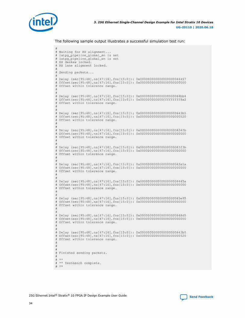
The following sample output illustrates a successful simulation test run:
# # Waiting for RX alignment...# iatpg_pipeline_global_en is set# iatpg_pipeline_global_en is set# RX deskew locked.# RX lane aligmnent locked.# # Sending packets...# # Delay (sec[95:48],ns[47:16],fns[15:0]): 0x000000000000000000064457# Offset(sec[95:48],ns[47:16],fns[15:0]): 0x000000000000000000000000# Offset within tolerence range.# # # Delay (sec[95:48],ns[47:16],fns[15:0]): 0x000000000000000000064bb4# Offset(sec[95:48],ns[47:16],fns[15:0]): 0x000000000000fffffffff8a2# Offset within tolerence range.# # # Delay (sec[95:48],ns[47:16],fns[15:0]): 0x0000000000000000000643b5# Offset(sec[95:48],ns[47:16],fns[15:0]): 0x000000000000000000000520# Offset within tolerence range.# # # Delay (sec[95:48],ns[47:16],fns[15:0]): 0x0000000000000000000634fb# Offset(sec[95:48],ns[47:16],fns[15:0]): 0x000000000000000000000000# Offset within tolerence range.# # # Delay (sec[95:48],ns[47:16],fns[15:0]): 0x000000000000000000063f3b# Offset(sec[95:48],ns[47:16],fns[15:0]): 0x000000000000000000000000# Offset within tolerence range.# # # Delay (sec[95:48],ns[47:16],fns[15:0]): 0x000000000000000000063a1a# Offset(sec[95:48],ns[47:16],fns[15:0]): 0x000000000000000000000000# Offset within tolerence range.# # # Delay (sec[95:48],ns[47:16],fns[15:0]): 0x00000000000000000006445a# Offset(sec[95:48],ns[47:16],fns[15:0]): 0x000000000000000000000000# Offset within tolerence range.# # # Delay (sec[95:48],ns[47:16],fns[15:0]): 0x000000000000000000063e95# Offset(sec[95:48],ns[47:16],fns[15:0]): 0x000000000000000000000000# Offset within tolerence range.# # # Delay (sec[95:48],ns[47:16],fns[15:0]): 0x0000000000000000000648d5# Offset(sec[95:48],ns[47:16],fns[15:0]): 0x000000000000000000000000# Offset within tolerence range.# # # Delay (sec[95:48],ns[47:16],fns[15:0]): 0x0000000000000000000643b5# Offset(sec[95:48],ns[47:16],fns[15:0]): 0x000000000000000000000520# Offset within tolerence range.# # # # Finished sending packets.# # **# ** Testbench complete.# **
3. 25G Ethernet Single-Channel Design Example for Intel Stratix 10 Devices
UG-20110 | 2020.06.18
25G Ethernet Intel® Stratix® 10 FPGA IP Design Example User Guide Send Feedback
34

Figure 19. Sample Simulation Output for Design Example with the IEEE 1588v2 Feature(Part 1 of 2)
3. 25G Ethernet Single-Channel Design Example for Intel Stratix 10 Devices
UG-20110 | 2020.06.18
Send Feedback 25G Ethernet Intel® Stratix® 10 FPGA IP Design Example User Guide
35
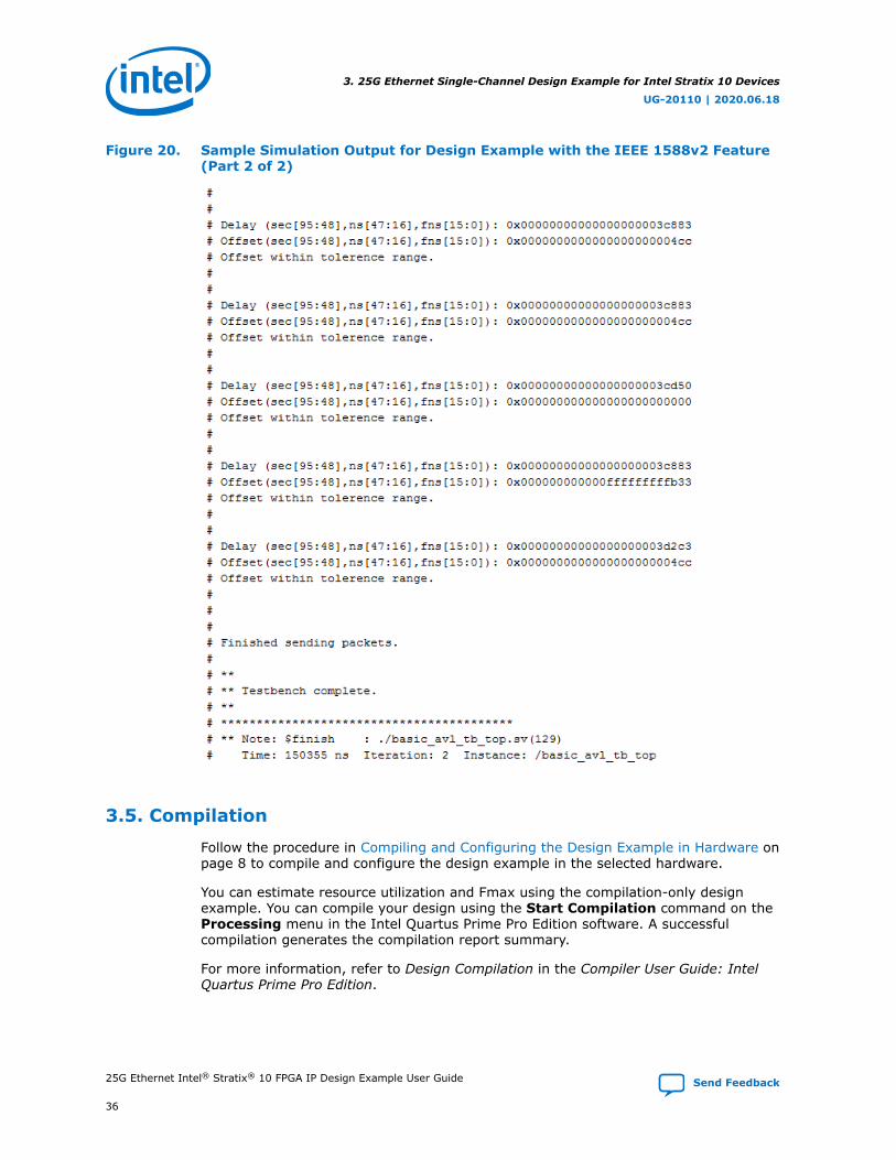
Figure 20. Sample Simulation Output for Design Example with the IEEE 1588v2 Feature(Part 2 of 2)
3.5. Compilation
Follow the procedure in Compiling and Configuring the Design Example in Hardware onpage 8 to compile and configure the design example in the selected hardware.
You can estimate resource utilization and Fmax using the compilation-only designexample. You can compile your design using the Start Compilation command on theProcessing menu in the Intel Quartus Prime Pro Edition software. A successfulcompilation generates the compilation report summary.
For more information, refer to Design Compilation in the Compiler User Guide: IntelQuartus Prime Pro Edition.
3. 25G Ethernet Single-Channel Design Example for Intel Stratix 10 Devices
UG-20110 | 2020.06.18
25G Ethernet Intel® Stratix® 10 FPGA IP Design Example User Guide Send Feedback
36

Related Information
Design CompilationIn Compiler User Guide: Intel Quartus Prime Pro Edition
3.6. Hardware Testing
In the hardware design example, you can program the IP core in internal serialloopback mode and generate traffic on the transmit side that loops back through thereceive side.
Follow the procedure at the provided related information link to test the designexample in the selected hardware.
Related Information
Testing the 25G Ethernet Intel FPGA IP Design in Hardware on page 10More information on the procedure and hardware setup.
3.6.1. Test Procedure—Design Example With and Without the IEEE1588v2 Feature
Follow these steps to test the design example in hardware:
1. Before you run the hardware testing for this design example, you must reset thesystem:
a. Click Tools ➤ In-System Sources & Probes Editor tool for the defaultSource and Probe GUI.
b. Toggle the system reset signal (Source[0]) from 0 to 1 to apply the resetand return the system reset signal back to 0 to release the system from thereset state.
c. Monitor the Probe signals and ensure that the status is valid.
2. To perform internal serial loopback test, refer to the Test Procedure—DesignExample Without the IEEE 1588v2 Feature section of the 10G/25G EthernetSingle-Channel Design Example for Intel Stratix 10 Devices chapter.
Related Information
• Design Example Registers on page 47
• Test Procedure—Design Example Without the IEEE 1588v2 Feature on page 23
3. 25G Ethernet Single-Channel Design Example for Intel Stratix 10 Devices
UG-20110 | 2020.06.18
Send Feedback 25G Ethernet Intel® Stratix® 10 FPGA IP Design Example User Guide
37
4. 25G Ethernet Multi-Channel Design Example for IntelStratix 10 Devices
The 25G Ethernet multi-channel design example demonstrates an Ethernet solution forIntel Stratix 10 devices using the 25G Ethernet Intel FPGA IP core.
Generate the design example from the Example Design tab of the 25G Ethernet IntelFPGA IP parameter editor.
4.1. Features
• Supports up to four Ethernet channels operating at 25G.
• Provides testbench and simulation script.
4.2. Hardware and Software Requirements
Intel uses the following hardware and software to test the design example in a Linuxsystem:
• Intel Quartus Prime Pro Edition software.
• ModelSim-SE, NCSim (Verilog only), VCS, and Xcelium simulator.
• Intel Stratix 10 GX Signal Integrity L-Tile (Production) Development Kit(1SX280LU2F50E1VG) for hardware testing.
4.3. Functional Description
The 25G Ethernet multi-channel design example consists of various components. Thefollowing block diagram shows the design components and the top-level signals of thedesign example.
UG-20110 | 2020.06.18
Send Feedback
Intel Corporation. All rights reserved. Agilex, Altera, Arria, Cyclone, Enpirion, Intel, the Intel logo, MAX, Nios,Quartus and Stratix words and logos are trademarks of Intel Corporation or its subsidiaries in the U.S. and/orother countries. Intel warrants performance of its FPGA and semiconductor products to current specifications inaccordance with Intel's standard warranty, but reserves the right to make changes to any products and servicesat any time without notice. Intel assumes no responsibility or liability arising out of the application or use of anyinformation, product, or service described herein except as expressly agreed to in writing by Intel. Intelcustomers are advised to obtain the latest version of device specifications before relying on any publishedinformation and before placing orders for products or services.*Other names and brands may be claimed as the property of others.
ISO9001:2015Registered

Figure 21. Block Diagram—25G Ethernet Multi-Channel Design Example (MAC+PCS+PMACore Variant)
25G Ethernet Multi-Channel Design Example
Source and ProbeSystem Reset(Full Design)
25G Ethernet Intel FPGA IP(MAC+PCS+PMA)
Intel Stratix 10 GX Signal Integrity L-Tile (Production) Development Kit
tx_serial_clk(12.890625 GHz)
Avalon Streaming TX
Avalon Streaming RXLoopback
Control and Status Interface
Transceiver PHYMAC+PCS
Client Logic(Packet Generator
and Monitor)
Control and Status Interface
Intel Stratix 10 DynamicReconfiguration Interface
SystemConsole
ATX PLL(25G)
ATX PLL(25G)
AvalonMemory-Mapped
Fabric
AvalonMemory-Mapped
JTAGto
Avalon Memory-MappedBridge
AvalonMemory-Mapped
4.3.1. Design Components
Table 11. Design Components
Component Description
25G Ethernet Intel FPGA IP Consists of MAC, PCS, and Transceiver PHY, with the following configuration:• Core Variant: MAC+PCS+PMA• Enable RS-FEC: Not selected• Enable flow control: Optional• Enable link fault generation: Optional• Enable preamble passthrough: Optional• Enable statistics collection: Optional• Enable MAC statistics counters: Optional• Enable IEEE 1588: Not selected• Enable 10G/25G dynamic rate switching: Not selected• Enable Native PHY Debug Master Endpoint (NPDME): Optional• Reference clock frequency: 644.531250/322.265625
ATX PLL Generates TX serial clocks for the 25G transceiver.
Client logic Consists of:• Traffic generator, which generates burst packets to the 25G Ethernet Intel FPGA IP core
for transmission.• Traffic monitor, which receives burst packets from the 25G Ethernet Intel FPGA IP core.
Source and Probe Source and probe signals, including system reset input signal, which you can use fordebugging.
4. 25G Ethernet Multi-Channel Design Example for Intel Stratix 10 Devices
UG-20110 | 2020.06.18
Send Feedback 25G Ethernet Intel® Stratix® 10 FPGA IP Design Example User Guide
39
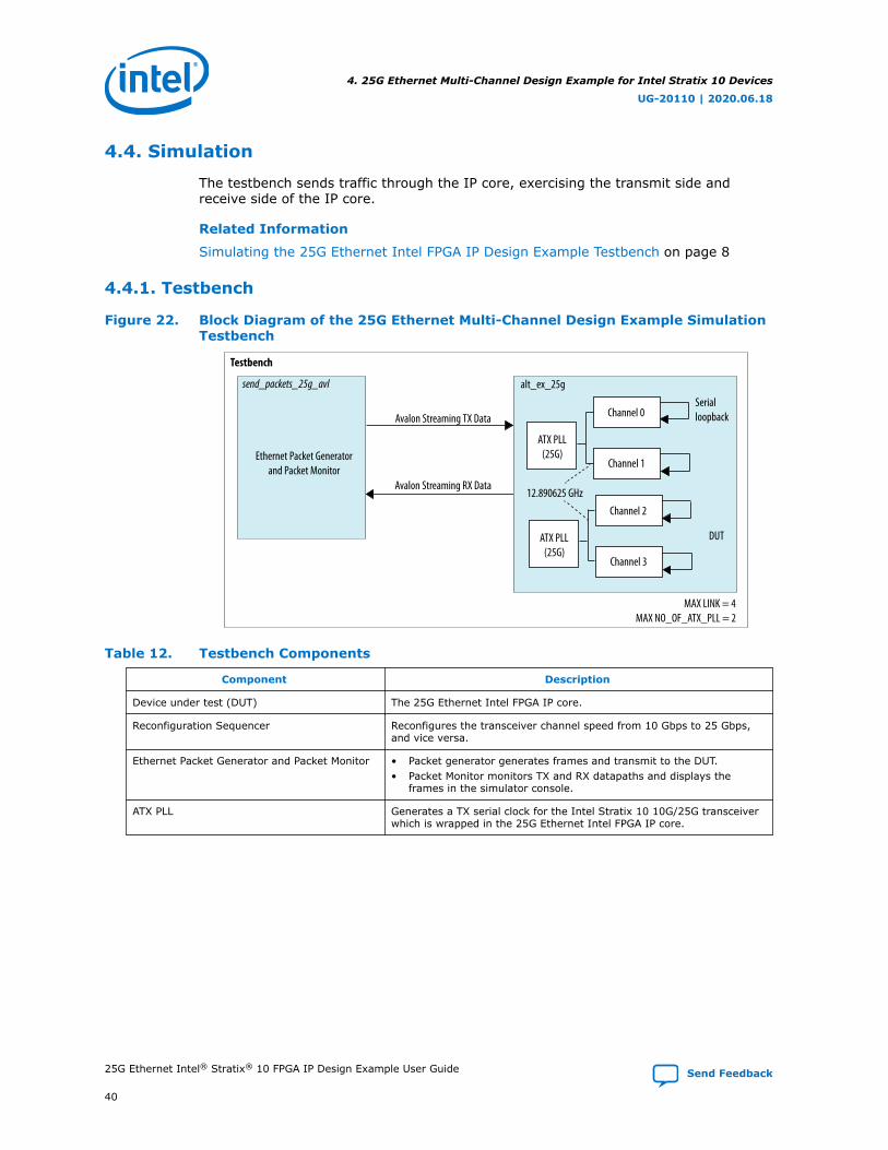
4.4. Simulation
The testbench sends traffic through the IP core, exercising the transmit side andreceive side of the IP core.
Related Information
Simulating the 25G Ethernet Intel FPGA IP Design Example Testbench on page 8
4.4.1. Testbench
Figure 22. Block Diagram of the 25G Ethernet Multi-Channel Design Example SimulationTestbench
Testbench
send_packets_25g_avl
Ethernet Packet Generatorand Packet Monitor
Avalon Streaming TX Data
Avalon Streaming RX Data
DUT
Serialloopback
ATX PLL(25G)
Channel 0
Channel 1
ATX PLL(25G)
Channel 2
Channel 3
12.890625 GHz
MAX LINK = 4MAX NO_OF_ATX_PLL = 2
alt_ex_25g
Table 12. Testbench Components
Component Description
Device under test (DUT) The 25G Ethernet Intel FPGA IP core.
Reconfiguration Sequencer Reconfigures the transceiver channel speed from 10 Gbps to 25 Gbps,and vice versa.
Ethernet Packet Generator and Packet Monitor • Packet generator generates frames and transmit to the DUT.• Packet Monitor monitors TX and RX datapaths and displays the
frames in the simulator console.
ATX PLL Generates a TX serial clock for the Intel Stratix 10 10G/25G transceiverwhich is wrapped in the 25G Ethernet Intel FPGA IP core.
4. 25G Ethernet Multi-Channel Design Example for Intel Stratix 10 Devices
UG-20110 | 2020.06.18
25G Ethernet Intel® Stratix® 10 FPGA IP Design Example User Guide Send Feedback
40
4.4.2. Simulation Design Example Components
Table 13. 25G Ethernet Multi-Channel Design Example Testbench File Descriptions
File Name Description
Testbench and Simulation Files
basic_avl_tb_top.v Top-level testbench file. The testbench instantiates the DUT,performs Avalon memory-mapped configuration on designcomponents and client logic, and sends and receives packetto or from the 25G Ethernet Intel FPGA IP.
Testbench Scripts
run_vsim.do The ModelSim script to run the testbench.
run_vcs.sh The Synopsys VCS script to run the testbench.
run_ncsim.sh The Cadence NCSim script to run the testbench.
run_xcelium.sh The Xcelium script to run the testbench.
4.4.3. Test Case
The simulation test case performs the following steps:
1. Instantiates 25G Ethernet Intel FPGA IP and ATX PLL.
2. Waits for PHY status signal to settle.
3. Prints PHY status.
4. Analyzes the results. The successful testbench sends and receives packets, anddisplays "Testbench complete."
4. 25G Ethernet Multi-Channel Design Example for Intel Stratix 10 Devices
UG-20110 | 2020.06.18
Send Feedback 25G Ethernet Intel® Stratix® 10 FPGA IP Design Example User Guide
41
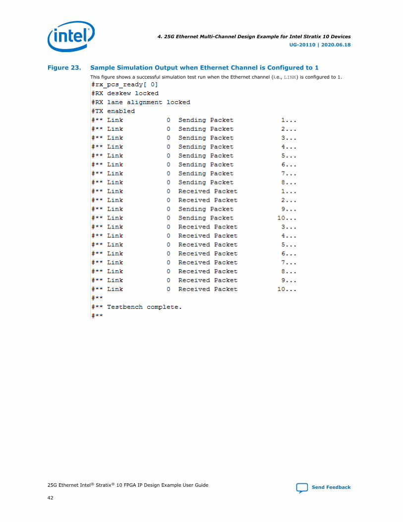
Figure 23. Sample Simulation Output when Ethernet Channel is Configured to 1This figure shows a successful simulation test run when the Ethernet channel (i.e., LINK) is configured to 1.
4. 25G Ethernet Multi-Channel Design Example for Intel Stratix 10 Devices
UG-20110 | 2020.06.18
25G Ethernet Intel® Stratix® 10 FPGA IP Design Example User Guide Send Feedback
42
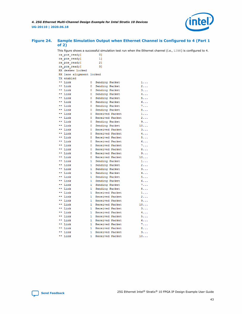
Figure 24. Sample Simulation Output when Ethernet Channel is Configured to 4 (Part 1of 2)This figure shows a successful simulation test run when the Ethernet channel (i.e., LINK) is configured to 4.
4. 25G Ethernet Multi-Channel Design Example for Intel Stratix 10 Devices
UG-20110 | 2020.06.18
Send Feedback 25G Ethernet Intel® Stratix® 10 FPGA IP Design Example User Guide
43
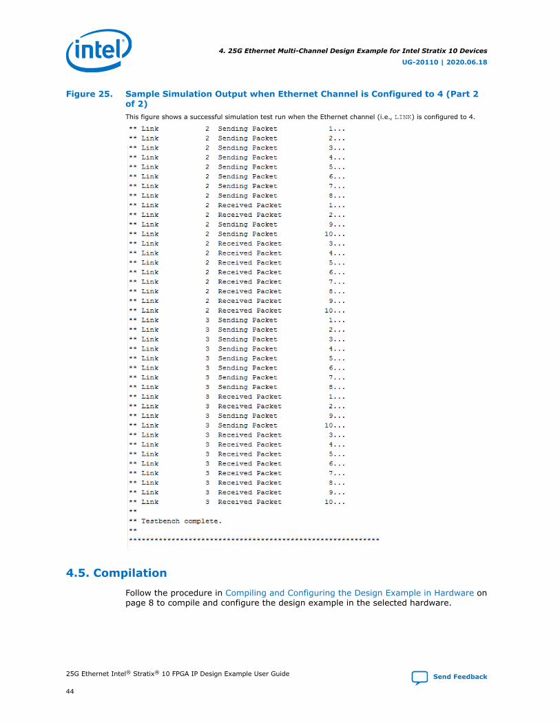
Figure 25. Sample Simulation Output when Ethernet Channel is Configured to 4 (Part 2of 2)This figure shows a successful simulation test run when the Ethernet channel (i.e., LINK) is configured to 4.
4.5. Compilation
Follow the procedure in Compiling and Configuring the Design Example in Hardware onpage 8 to compile and configure the design example in the selected hardware.
4. 25G Ethernet Multi-Channel Design Example for Intel Stratix 10 Devices
UG-20110 | 2020.06.18
25G Ethernet Intel® Stratix® 10 FPGA IP Design Example User Guide Send Feedback
44
You can estimate resource utilization and Fmax using the compilation-only designexample. You can compile your design using the Start Compilation command on theProcessing menu in the Intel Quartus Prime Pro Edition software. A successfulcompilation generates the compilation report summary.
For more information, refer to Design Compilation in the Compiler User Guide: IntelQuartus Prime Pro Edition.
Related Information
Design CompilationIn Compiler User Guide: Intel Quartus Prime Pro Edition
4.6. Hardware Testing
In the hardware design example, you can program the IP core in internal serialloopback mode and generate traffic on the transmit side that loops back through thereceive side.
Follow the procedure at the provided related information link to test the designexample in the selected hardware.
Related Information
Testing the 25G Ethernet Intel FPGA IP Design in Hardware on page 10More information on the procedure and hardware setup.
4.6.1. Test Procedure
Follow these steps to test the design example in hardware:
1. Before you run the hardware testing for this design example, you must reset thesystem:
a. Click Tools ➤ In-System Sources & Probes Editor tool for the defaultSource and Probe GUI.
b. Toggle the system reset signal (Source[0]) from 0 to 1 to apply the resetand return the system reset signal back to 0 to release the system from thereset state.
c. Monitor the Probe signals and ensure that the status is valid.
2. To perform internal serial loopback test, refer to the Test Procedure—DesignExample Without the IEEE 1588v2 Feature section of the 10G/25G EthernetSingle-Channel Design Example for Intel Stratix 10 Devices chapter.
Note: link_num is valid for 0 to 3 only.
Related Information
• Design Example Registers on page 47
• Test Procedure—Design Example Without the IEEE 1588v2 Feature on page 23
4. 25G Ethernet Multi-Channel Design Example for Intel Stratix 10 Devices
UG-20110 | 2020.06.18
Send Feedback 25G Ethernet Intel® Stratix® 10 FPGA IP Design Example User Guide
45

5. 25G Ethernet Intel FPGA IP Design Example ReferencesThis section provides information about the 25G Ethernet Intel FPGA IP core interfacesignals and registers in the design examples.
5.1. Design Example Interface Signals
The 25G Ethernet Intel FPGA IP core testbench is self-contained and does not requireyou to drive any input signals.
Table 14. Hardware Design Example Interface Signals for 25G Ethernet Intel FPGA IPCore for Intel Stratix 10 Devices
Signal Direction Comments
clk100 Input Drive at 100 MHz. The intent is to drive this from a 100Mhz oscillator on the board.
clk_ref Input Drive at 644.53125 MHz or 322.265625 MHz from anoscillator on the board.
cpu_resetn Input Resets the IP core. Active low. Drives the global hardreset csr_reset_n to the IP core.
tx_serial Output Transceiver PHY output serial data.
rx_serial Input Transceiver PHY input serial data.
user_led[7:0] Output
Status signals. The hardware design example connectsthese bits to drive LEDs on the target board. Individualbits reflect the following signal values and clockbehavior:• [0]: Main reset signal to IP core• [1]: Reserved• [2]: Divided version of clk50• [3]: Divided version of 100 MHz status clock• [4]: tx_lanes_stable• [5]: rx_block_lock• [6]: rx_am_lock• [7]: rx_pcs_ready
Related Information
Interfaces and Signal DescriptionsProvides detailed descriptions of the Intel Stratix 10 core signals and the interfacesto which they belong.
UG-20110 | 2020.06.18
Send Feedback
Intel Corporation. All rights reserved. Agilex, Altera, Arria, Cyclone, Enpirion, Intel, the Intel logo, MAX, Nios,Quartus and Stratix words and logos are trademarks of Intel Corporation or its subsidiaries in the U.S. and/orother countries. Intel warrants performance of its FPGA and semiconductor products to current specifications inaccordance with Intel's standard warranty, but reserves the right to make changes to any products and servicesat any time without notice. Intel assumes no responsibility or liability arising out of the application or use of anyinformation, product, or service described herein except as expressly agreed to in writing by Intel. Intelcustomers are advised to obtain the latest version of device specifications before relying on any publishedinformation and before placing orders for products or services.*Other names and brands may be claimed as the property of others.
ISO9001:2015Registered
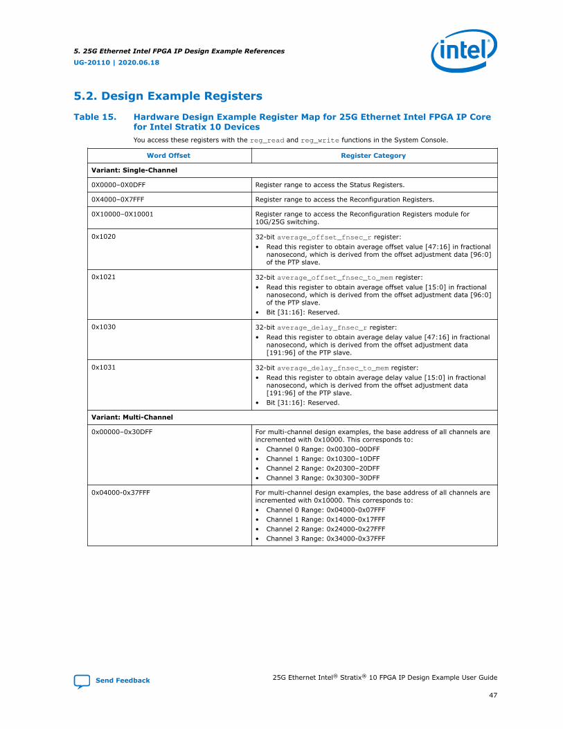
5.2. Design Example Registers
Table 15. Hardware Design Example Register Map for 25G Ethernet Intel FPGA IP Corefor Intel Stratix 10 DevicesYou access these registers with the reg_read and reg_write functions in the System Console.
Word Offset Register Category
Variant: Single-Channel
0X0000–0X0DFF Register range to access the Status Registers.
0X4000–0X7FFF Register range to access the Reconfiguration Registers.
0X10000–0X10001 Register range to access the Reconfiguration Registers module for10G/25G switching.
0x1020 32-bit average_offset_fnsec_r register:• Read this register to obtain average offset value [47:16] in fractional
nanosecond, which is derived from the offset adjustment data [96:0]of the PTP slave.
0x1021 32-bit average_offset_fnsec_to_mem register:• Read this register to obtain average offset value [15:0] in fractional
nanosecond, which is derived from the offset adjustment data [96:0]of the PTP slave.
• Bit [31:16]: Reserved.
0x1030 32-bit average_delay_fnsec_r register:• Read this register to obtain average delay value [47:16] in fractional
nanosecond, which is derived from the offset adjustment data[191:96] of the PTP slave.
0x1031 32-bit average_delay_fnsec_to_mem register:• Read this register to obtain average delay value [15:0] in fractional
nanosecond, which is derived from the offset adjustment data[191:96] of the PTP slave.
• Bit [31:16]: Reserved.
Variant: Multi-Channel
0x00000–0x30DFF For multi-channel design examples, the base address of all channels areincremented with 0x10000. This corresponds to:• Channel 0 Range: 0x00300–00DFF• Channel 1 Range: 0x10300–10DFF• Channel 2 Range: 0x20300–20DFF• Channel 3 Range: 0x30300–30DFF
0x04000-0x37FFF For multi-channel design examples, the base address of all channels areincremented with 0x10000. This corresponds to:• Channel 0 Range: 0x04000-0x07FFF• Channel 1 Range: 0x14000-0x17FFF• Channel 2 Range: 0x24000-0x27FFF• Channel 3 Range: 0x34000-0x37FFF
5. 25G Ethernet Intel FPGA IP Design Example References
UG-20110 | 2020.06.18
Send Feedback 25G Ethernet Intel® Stratix® 10 FPGA IP Design Example User Guide
47
Note: 1. For Intel Stratix 10 H-tile production device, disable the background calibrationprior to accessing the transceiver core reconfiguration register, as described in theDisabling Background Calibration section of the 25G Ethernet Intel FPGA IP UserGuide.
2. Dynamic reconfiguration switching for 10G/25G is not available for multi-channeldesigns.
3. For single-channel design example, 0x4000 is the base address of the PHYregisters. For example, to read the background calibration register, typereg_read 0x4542.
4. For multi-channel design example, the base address of the PHY registers is0x4000 + (0x10000 * <link num>). For example, to read the backgroundcalibration register at channel 2, type reg_read 0x24542.
Related Information
• Control, Status, and Statistics Register Descriptions section of the 25G EthernetIntel FPGA IP User Guide
Describes the 25G Ethernet Intel FPGA IP control, status, and statisticsregisters.
• Disabling Background Calibration section of the 25G Ethernet Intel FPGA IP UserGuide
5.3. Using Transceiver Toolkit on H-Tile Production Device
If your design example targets the H-tile production device and Enable autoadaptation triggering for RX PMA CTLE/DFE mode option is turned on, you mustperform additional steps to configure the register 0x343 bit[0] before you can use theTransceiver Toolkit. Refer to the description for register 0x343 in the 25G EthernetIntel Stratix 10 FPGA IP User Guide for more information.
Follow these steps to use Transceiver Toolkit:
1. Follow the procedure in the Testing the 25G Ethernet Intel FPGA IP Design inHardware section to load the main.tcl script.
2. For single-channel design example, type reg_write 0x343 0x1 to hold the autoadaptation module FSM in idle state.
3. For multi-channel design example,
a. type reg_write 0x343 0x1 for channel 0
b. type reg_write 0x10343 0x1 for channel 1
c. type reg_write 0x20343 0x1 for channel 2
d. type reg_write 0x30343 0x1 for channel 3
4. Launch the Transceiver Toolkit.
Note: If the register 0x343 bit[0] is not set (1'b1), the transceiver channel is not visible inthe Transceiver Toolkit.
Follow these steps after you already used the Transceiver Toolkit:
5. 25G Ethernet Intel FPGA IP Design Example References
UG-20110 | 2020.06.18
25G Ethernet Intel® Stratix® 10 FPGA IP Design Example User Guide Send Feedback
48
1. Close the Transceiver Toolkit.
2. For single-channel design example, type reg_write 0x343 0x0 to re-start theauto adaptation module FSM.
3. For multi-channel design example,
a. type reg_write 0x343 0x0 for channel 0
b. type reg_write 0x10343 0x0 for channel 1
c. type reg_write 0x20343 0x0 for channel 2
d. type reg_write 0x30343 0x0 for channel 3
Note: If the register 0x343 bit[0] is cleared (1'b0) when you opened the Transceiver Toolkit,the System Console may hang.
Related Information
• 25G Ethernet Intel Stratix 10 FPGA IP User Guide
• Testing the 25G Ethernet Intel FPGA IP Design in Hardware on page 10
5. 25G Ethernet Intel FPGA IP Design Example References
UG-20110 | 2020.06.18
Send Feedback 25G Ethernet Intel® Stratix® 10 FPGA IP Design Example User Guide
49

6. 25G Ethernet Intel Stratix 10 FPGA IP Design ExampleUser Guide Archives
IP versions are the same as the Intel Quartus Prime Design Suite software versions upto v19.1. From Intel Quartus Prime Design Suite software version 19.2 or later, IPcores have a new IP versioning scheme.If an IP core version is not listed, the user guide for the previous IP core version applies.
Intel Quartus PrimeVersion
IP Core Version User Guide
19.1 19.1 25G Ethernet Intel Stratix 10 FPGA IP Design Example User Guide
18.1 18.1 25G Ethernet Intel Stratix 10 FPGA IP Design Example User Guide
18.0 18.0 25G Ethernet Intel Stratix 10 FPGA IP Design Example User Guide
UG-20110 | 2020.06.18
Send Feedback
Intel Corporation. All rights reserved. Agilex, Altera, Arria, Cyclone, Enpirion, Intel, the Intel logo, MAX, Nios,Quartus and Stratix words and logos are trademarks of Intel Corporation or its subsidiaries in the U.S. and/orother countries. Intel warrants performance of its FPGA and semiconductor products to current specifications inaccordance with Intel's standard warranty, but reserves the right to make changes to any products and servicesat any time without notice. Intel assumes no responsibility or liability arising out of the application or use of anyinformation, product, or service described herein except as expressly agreed to in writing by Intel. Intelcustomers are advised to obtain the latest version of device specifications before relying on any publishedinformation and before placing orders for products or services.*Other names and brands may be claimed as the property of others.
ISO9001:2015Registered

7. Document Revision History for the 25G Ethernet IntelStratix 10 FPGA IP Design Example User Guide
Document Version Intel QuartusPrime Version
IP Version Changes
2020.06.18 19.2 19.2.0 • Updated the following Figures:— Block Diagram—10G/25G Ethernet Single-
Channel Design Example (MAC+PCS+PMA CoreVariant) Without the IEEE 1588v2 Feature
— Block Diagram—10G/25G Ethernet Single-Channel Design Example (MAC+PCS+PMA CoreVariant) with the IEEE 1588v2 Feature
— Block Diagram—10G/25G Ethernet Single-Channel Design Example (MAC+PCS CoreVariant) Without the IEEE 1588v2 Feature
— Block Diagram—10G/25G Ethernet Single-Channel Design Example (MAC+PCS CoreVariant) with the IEEE 1588v2 Feature
— Block Diagram—25G Ethernet Single-ChannelDesign Example (MAC+PCS+PMA Core Variant)Without the IEEE 1588v2 Feature
— Block Diagram—25G Ethernet Single-ChannelDesign Example (MAC+PCS+PMA Core Variant)with the IEEE 1588v2 Feature
— Block Diagram—25G Ethernet Single-ChannelDesign Example (MAC+PCS Core Variant)Without the IEEE 1588v2 Feature
— Block Diagram—25G Ethernet Single-ChannelDesign Example (MAC+PCS Core Variant) withthe IEEE 1588v2 Feature
— Block Diagram—25G Ethernet Multi-ChannelDesign Example (MAC+PCS+PMA Core Variant)
• Updated the document for latest Intel brandingstandards.
2020.04.13 19.2 19.2.0 Added new topic—Using Transceiver Toolkit on H-TileProduction Device.
2020.02.14 19.2 19.2.0 Updated the procedure steps in the Changing TargetDevice in Hardware Design Example section.
continued...
UG-20110 | 2020.06.18
Send Feedback
Intel Corporation. All rights reserved. Agilex, Altera, Arria, Cyclone, Enpirion, Intel, the Intel logo, MAX, Nios,Quartus and Stratix words and logos are trademarks of Intel Corporation or its subsidiaries in the U.S. and/orother countries. Intel warrants performance of its FPGA and semiconductor products to current specifications inaccordance with Intel's standard warranty, but reserves the right to make changes to any products and servicesat any time without notice. Intel assumes no responsibility or liability arising out of the application or use of anyinformation, product, or service described herein except as expressly agreed to in writing by Intel. Intelcustomers are advised to obtain the latest version of device specifications before relying on any publishedinformation and before placing orders for products or services.*Other names and brands may be claimed as the property of others.
ISO9001:2015Registered
Document Version Intel QuartusPrime Version
IP Version Changes
2019.12.13 19.2 19.2.0 Updated the procedure steps in the Changing TargetDevice in Hardware Design Example section.
2019.08.29 19.2 19.2.0 Updated the instruction for the ModelSim simulator inTable: Steps to Simulate the Testbench.
2019.07.01 19.2 19.2.0 • Added new topic—Changing Target Device inHardware Design Example.
• Updated references to Intel Stratix 10 L-Tile GXTransceiver Signal Integrity Development Kit (OPN:1SX280LU2F50E2VG) as Intel Stratix 10 GX SignalIntegrity L-Tile (Production) Development Kit (OPN:1SX280LU2F50E1VG).
• Updated the Generating the Design Example topicto add a note to Step 8.
• Updated Figure: Example Design Tab in the 25GEthernet Intel FPGA IP Parameter Editor.
• Updated the Hardware and Software Requirementstopics for all design example chapters.
Document Version Intel QuartusPrime Version
Changes
2019.05.10 19.1 • Renamed Altera Debug Master Endpoint (ADME) to Native PHY DebugMaster Endpoint (NPDME).
• Updated the hardware testing steps for the following topics:— Test Procedure—Design Example Without the IEEE 1588v2 Feature
for 10G/25G Ethernet single-channel design example.— Test Procedure—Design Example with the IEEE 1588v2 Feature for
10G/25G Ethernet single-channel design example.— Test Procedure—Design Example With and Without the IEEE 1588v2
Feature for 25G Ethernet single-channel design example.— Test Procedure for 25G Ethernet multi-channel design example.
• Updated the following Figures:— Block Diagram—10G/25G Ethernet Single-Channel Design Example
(MAC+PCS+PMA Core Variant) Without the IEEE 1588v2 Feature— Block Diagram—10G/25G Ethernet Single-Channel Design Example
(MAC+PCS+PMA Core Variant) with the IEEE 1588v2 Feature— Block Diagram—10G/25G Ethernet Single-Channel Design Example
(MAC+PCS Core Variant) Without the IEEE 1588v2 Feature— Block Diagram—10G/25G Ethernet Single-Channel Design Example
(MAC+PCS Core Variant) with the IEEE 1588v2 Feature
continued...
7. Document Revision History for the 25G Ethernet Intel Stratix 10 FPGA IP Design ExampleUser Guide
UG-20110 | 2020.06.18
25G Ethernet Intel® Stratix® 10 FPGA IP Design Example User Guide Send Feedback
52

Document Version Intel QuartusPrime Version
Changes
• Updated Table: Hardware Design Example Register Map for 25GEthernet Intel FPGA IP Core for Intel Stratix 10 Devices to includereconfiguration registers (0x04000-0x37FFF).
• Updated the note section in the Design Example Registers topic.• Made editorial updates throughout the document.
2019.01.07 18.1 • Updated the Generating the Design Example topic to correct targetdevelopment kit in Step 8 from Stratix 10 GX FPGA DevelopmentKit to Intel Stratix 10 L-Tile GX Transceiver Signal IntegrityDevelopment Kit.
• Updated Figure: Block Diagram—10G/25G Ethernet Single-ChannelDesign Example (MAC+PCS+PMA Core Variant) with the IEEE 1588v2Feature.
• Added a note to Design Example Registers topic.
2018.10.03 18.1 • Updated Table: Parameters in the Example Design Tab to update thedescription for Select Board.
• Updated the Hardware and Software Requirements topics for all designexample chapters.
• Updated the Design Components topics for all design example chapters.• Added new Figures:
— Block Diagram—25G Ethernet Single-Channel Design Example (MAC+PCS Core Variant) Without the IEEE 1588v2 Feature
— Block Diagram—25G Ethernet Single-Channel Design Example (MAC+PCS Core Variant) Without the IEEE 1588v2 Feature
— Block Diagram—25G Ethernet Single-Channel Design Example (MAC+PCS Core Variant) Without the IEEE 1588v2 Feature
— Block Diagram—25G Ethernet Single-Channel Design Example (MAC+PCS Core Variant) with the IEEE 1588v2 Feature
• Updated Figures:— Example Design Tab in the 25G Ethernet Intel FPGA IP Parameter
Editor— Block Diagram—25G Ethernet Single-Channel Design Example (MAC
+PCS+PMA Core Variant) with the IEEE 1588v2 Feature— Block Diagram—25G Ethernet Single-Channel Design Example (MAC
+PCS+PMA Core Variant) Without the IEEE 1588v2 Feature— Block Diagram—25G Ethernet Multi-Channel Design Example (MAC
+PCS+PMA Core Variant)— Block Diagram—10G/25G Ethernet Single-Channel Design Example
(MAC+PCS+PMA) Without the IEEE 1588v2 Feature— Block Diagram—10G/25G Ethernet Single-Channel Design Example
(MAC+PCS+PMA) with the IEEE 1588v2 Feature• Removed Figure: Sample Simulation Output for Design Example with
the IEEE 1588v2 Feature (Part 1 of 2) and Sample Simulation Outputfor Design Example with the IEEE 1588v2 Feature (Part 2 of 2).
• Updated the simulation sample output of the Test Case—DesignExample with the IEEE 1588v2 Feature topic for 25G Ethernet Single-Channel design example.
• Updated the simulation sample output of the Test Case—DesignExample with the IEEE 1588v2 Feature topic for the 10G/25G Ethernetdesign example.
• Restructured descriptions for Features topics for all design examplechapters.
• Streamlined the contents and document organization.
2018.06.25 18.0 Initial release.
7. Document Revision History for the 25G Ethernet Intel Stratix 10 FPGA IP Design ExampleUser Guide
UG-20110 | 2020.06.18
Send Feedback 25G Ethernet Intel® Stratix® 10 FPGA IP Design Example User Guide
53