Embed Size (px)
Citation preview

8/8/2019 26924074 Laboratory 6 Basic Op Amp Circuits
http://slidepdf.com/reader/full/26924074-laboratory-6-basic-op-amp-circuits 1/10
6-1
LABORATORY 6
BASIC OP-AMP CIRCUITS
OBJECTIVES
1. To study the ac characteristics of the open loop op-amp configuration.
2. To study the ac characteristics of the non-inverting op-amp configuration.3. To study the ac characteristics of the inverting op-amp configuration.
4. To study the ac characteristics of the integrator op-amp configuration.
5. To simulate the integrator, non-inverting and inverting op-amp circuits using Micro-Cap
software.
INFORMATION
Note: Actual lab procedure follows this information section.
The integrated circuit operational amplifier (op-amp) is an extremely versatile electronicdevice, which is encountered in a wide variety of applications ranging from consumer electronics
(stereos, VCR’s) to complex commercial applications and industrial controls. This versatility
stems from the very high voltage gain (100,000 and higher for the 741) together with high input
resistance (typically 1 MW) and low output resistance (typically 50W). These characteristics
allow use of large amounts of feedback from output to input with the result that the desired
output signal is dependent only on the external components.Op-amps are direct coupled devices such that the input signal may be either AC or DC, or
a combination of the two. The industrial standard op-amp, the 741, requires two power supplies,
one positive and one negative. For most applications the magnitude of these two voltages is thesame. All op-amps have two inputs connected in a differential mode, so that output voltage is
Vo= A(V+ - V-) where V+ is the voltage at the non-inverting input and V- is the voltage at the
inverting input. A is the open loop gain of the op-amp.
The circuit symbol for an op-amp is shown in Figure 6.1. The pin connections for the 8 pin DIP
package mA741 op-amp are given in Figure 6.2.
Chip Diagrams:
Figure 6.1 Symbol for a basic op-amp Figure 6.2 The m A741 op-amp package.
Ideally, an op-amp will have infinite open loop voltage gain A, infinite input resistance
R in and zero output resistance Ro. The input currents in the two differential inputs and the
Vcc+
uA 741
6
OUT
IN-
8
-
7
+
2
Vcc-IN+
3 4
5
1
_ OUT+
IN-
IN+
Vcc+
Vcc-

8/8/2019 26924074 Laboratory 6 Basic Op Amp Circuits
http://slidepdf.com/reader/full/26924074-laboratory-6-basic-op-amp-circuits 2/10
6-2
voltage difference between the two inputs will be vanishingly small. In practice these quantities
are finite and in most applications can be ignored.
1. Basic non-inverting amplifier
The basic non-inverting op-amp configuration is shown in Figure 6.3. You can achieve a
particular value of the gain Av of the non-inverting amplifier by choosing the R1 and R2 values.
The theoretical ideal characteristics are determined largely by the external biasing resistors, andare given by Equations (6.1), (6.2) and (6.3).
Rin = ¥ W Equation (6.1)
Ro = 0 W Equation (6.2)
1
21 R
R Av += Equation (6.3)
Figure 6.3 Basic non-inverting amplifier
2. Basic inverting amplifier
The basic inverting op-amp configuration is shown in Figure 6.4. You can achieve a particular
value of the gain Av of the inverting amplifier by choosing the R1 and R2 values.
Figure 6.4 Basic inverting amplifier
The theoretical ideal characteristics are determined largely by the external biasing resistors, andare given by Equations (6.4), (6.5) and (6.6).
Rin = R 1 Equation (6.4.)
Ro = 0 W Equation (6.5.)
1
2
R
R Av -= Equation (6.6.)
_ Vout
+
Vcc+
Vcc-Vin
R2
R1
Vin
R2
R1 _
Vout
+
Vcc+
Vcc-

8/8/2019 26924074 Laboratory 6 Basic Op Amp Circuits
http://slidepdf.com/reader/full/26924074-laboratory-6-basic-op-amp-circuits 3/10
6-3
3. Basic integrator circuit
The standard integrator using an ideal op-amp is given in Figure 6.5. A practical op-amp at low
frequencies has small DC off-set voltages and currents, which can create havoc with the outputof an integrator circuit. The integrator may saturate and the output voltage becomes pegged at
either the positive or negative saturation level. To overcome this difficulty a bleeder resistance
R2 is added as shown in Figure 6.6. The frequency range of the integrator will now be limited, because at low frequencies the circuit will act as an amplifier.
The function of an integrator is to perform mathematical integration upon the input. A square
wave, when integrated, will become triangular. A triangular wave, when integrated, will becomea parabolic waveform, which is close to a sine wave.
Figure 6.5 The ideal integrator circuit Figure 6.6 Practical integrator circuit
EQUIPMENT1. Digital multimeter (Fluke 8010A, BK PRECISION 2831B or BK PRECISION 2831C)
2. PROTO-BOARD PB-503 (breadboard)
3. Digital Oscilloscope Tektronix TDS 210
4. Function Generator Wavetek FG3B
5. Dual Voltage Power Supply
6. Resistors: 10 k W, 270 k W, 2.2k W
7. Capacitor 470pF
8.
uA741 op-amp
PRE-LABORATORY PREPARATION
The lab preparation must be completed before coming to the lab. Show it to your TA for check
at the beginning of the lab and get his/her signature in the Signature section of the Lab
Measurements Sheet. The penalty for incomplete preparations is 20%.
During your pre-lab you must prepare several Micro-Cap simulations and plot the input andoutput waveforms for different op-amp applications. Please refer to the following remarks for
Micro-Cap circuit set up and simulation:
· For a sine wave signal source (used for simulating the circuits in Figures 6.8 and 6.9), use a1MHz Sinusoidal Source from the Micro–Cap library. Set the required frequency toF=1k (Hz) and the AC Amplitude to A= 0.2(V) in the model description area of the signal
source. Note that A=0.2V corresponds to a magnitude of Vp-p=0.4V.
· For a square wave signal source (for simulating Figure 6.11), use the Square Source fromthe Micro-Cap library. Set the required amplitude and frequency of the square wave signal by changing the amplitude, duration and repetition period of the pulse sequence in the model
description area of the square wave signal source. For a 1 kHz square signal, set the pulse
parameters as follows: P1=0, P2=0, P3=500U, P4=500U and P5=1M.
R2
Vin Vout
Vcc-
R1
C1
Vcc+
+
_ Vin Vout
Vcc-
R1
C1
Vcc+
+
_

8/8/2019 26924074 Laboratory 6 Basic Op Amp Circuits
http://slidepdf.com/reader/full/26924074-laboratory-6-basic-op-amp-circuits 4/10
6-4
Set the signal amplitude in fields VZERO to -0.2(V) and VONE to 0.2(V). Note that this
corresponds to a magnitude of Vp-p = 0.4V.
· To obtain input and output waveforms for certain circuits, you must run “TRANSIENTANALYSIS”. To get the best results for your plots set the Transient Analysis Limits as
follows:Ø Time parameters: Time Range = 5m;
Maximum Time Step = 0.00001;
Ø Plot parameters: P X-Expression Y-Expression X-Range Y-Range
Input signal 1 T V(1)* 5m,0,0.5m 0.3,-0.3,0.1
Output signal 2 T V(2)* 5m,0,0.5m 8,-8,2
Note: * V(1) and V(2) are the AC voltages at corresponding nodes (1) and (2) of the
simulation circuit set up. In your particular case they could have different numeration.
The following Micro-Cap simulations and plots of the input and output waveforms for differentop amp applications must be prepared for your pre-lab:
1. [8 MARKS] Simulate the non-inverting amplifier shown in Figure 6.8. Plot both theoutput and input waveforms for a sine waveform input signal with Vin p-p=0.4V at 1kHz.
2. [3 MARKS] From your plots calculate the voltage gain Av of the non-inverting amplifier
circuit. Also calculate the theoretical voltage gain Av using Equation (6.3). Enter the
values in Table 6.1 of the Lab Measurements Sheet.3. [8 MARKS] Simulate the inverting amplifier shown in Figure 6.9. Plot both the output
and input waveforms for a sine waveform input signal with Vin p-p=0.4V at 1kHz.
4. [3 MARKS] From your plots calculate the voltage gain Av of the inverting amplifier
circuit. Also calculate the theoretical voltage gain Av using Equation (6.6). Enter thevalues in Table 6.2 of the Lab Measurements Sheet.
5. [8 MARKS] Simulate the real integrator circuit shown in Figure 6.11. Plot both the
output and input waveforms for a square waveform input signal with Vin p-p =0.4V at1kHz.
Note: For each simulation, print the Micro-Cap circuit set-up with node numbers and the supplementary text file with components description. This will help your TA to correct any mistakesin your simulations. Bring all required plots to your lab session and submit them to your TA. Youwill use these plots to draw practical results of your experiments during the lab session.
PROCEDURE
The pin connections for the 8 pin DIP package uA741 op-amp are given in Figure 6.2.Throughout this experiment use the external dual DC Power Supply Unit shown in Figure 6.7.
Use the dual trace oscilloscope to observe the shape and to measure the amplitude of the inputand output waveforms.
To use the Power Supply Unit:
· Turn the Power Supply ON. Adjust the voltage of the Power Supply to 12V. Thiswill set both positive and negative power sources respectively to +12V and –12V.
· Turn the Power Supply OFF before connecting to the circuits.

8/8/2019 26924074 Laboratory 6 Basic Op Amp Circuits
http://slidepdf.com/reader/full/26924074-laboratory-6-basic-op-amp-circuits 5/10
6-5
· Connect the POS terminal of the Power Supply to the Vcc+ of your circuit.Connect the NEG terminal of the Power Supply to the Vcc- of your circuit. Connect
the COM terminal of the Power Supply to the ground of your circuit
Figure 6.7 Front panel of power supply unit
1. Non-inverting amplifier measurements
1.1. Build the circuit of Figure 6.8 using an 8-pin uA741 op-amp with R 1 = 10k W, R 2 = 270 k W.
When the layout has been completed, have your TA check your breadboard for errors and
get his/her signature in the Signature section of the Lab Measurements Sheet. You will be
penalized marks if your sheet is not initialed.1.2. Apply a 1kHz sinusoidal voltage signal from the Signal Generator to the input and use thedual trace oscilloscope to observe both input and output waveforms. Adjust the magnitude of the
input signal until clipping occurs on either the positive or negative peak of the output voltage.
Determine the maximum possible ac voltage swing, i.e. maximum peak to peak voltage that can
be obtained at the output of the circuit without clipping. Compare this to the DC power supplyvoltages. Put this information in section 1.1 of the Lab Measurements Sheet.
1.3. For Vin p-p=0.4V at F=1kHz measure the amplitude of the output signal Vout and calculate
voltage gain of this circuit. Record data and compare the values with pre-lab calculations inTable 6.1 of the Lab Measurements Sheet.
1.4. Draw the input and output waveforms on top of your simulations plots. In section 1.3 of the
Lab Measurements Sheet compare how close your practical results are to the simulations
Figure 6.8 Measurement circuit for non-inverting amplifier
1.5. Turn the oscilloscope into “XY Mode”* and observe the curve on its display. Vary the input
signal amplitude and explain what happens when you change the magnitude of the input signal
before and after the output signal becomes saturated. Draw the XY waveform in Figure 6.12 insection 1.4 and answer question in section 1.5 of the Lab Measurements Sheet.
* To turn the oscilloscope into “XY Mode”, first press the “DISPLAY” button and then by
pressing the soft button “FORMAT”, assigned to display, choose “XY” mode. You can
ADJUST
P OS C OM N EG GNDON
OFF
uA741
+12V
_
+
CH-2
CH-1
Vin
-12V
Vout
SIGNAL
10k
2
270k
GENERATOR
R2
3
CH 2
4
7R1
R3
2.2k
6
1kHz
CH 1

8/8/2019 26924074 Laboratory 6 Basic Op Amp Circuits
http://slidepdf.com/reader/full/26924074-laboratory-6-basic-op-amp-circuits 6/10
6-6
confirm that you are in the correct mode if an “XY Mode” notice is displayed in the
bottom right corner of the oscilloscope’s display.
2. Inverting amplifier measurements
2.1. Build the circuit of Figure 6.9 using an 8-pin uA741 op-amp with R 1 = 10k W, R 2 = 270 k W.
When the layout has been completed, have your TA check your breadboard for errors and
get his/her signature in the Signature section of the Lab Measurements Sheet. You will be penalized marks if your sheet is not initialed.
2.2. Apply a 1kHz sinusoidal voltage signal from the Signal Generator to the input and use thedual trace oscilloscope to observe the shape and to measure the amplitude of the input and output
waveforms.
2.3. For Vin p-p=0.4V at F=1kHz measure the amplitude of the output signal Vout and calculatevoltage gain of this circuit. Record data and compare the values with pre-lab calculations in
Table 6.2 in section 2.1 of the Lab Measurements Sheet.
Figure 6.9 Measurement circuit for inverting amplifier
2.4. Draw the input and output waveforms on top of your simulations plots. In section 2.2 of the
Lab Measurements Sheet compare how close your practical results are to the simulations.
2.5. Input resistance measurements.Using a Digital Multimeter, measure the AC input current of the inverting amplifier, as shown in
Figure 6.10. Read the input voltage RMS* value on your oscilloscope. Record the measured
values and calculations in Table 6.3 at section 2.3 of the Lab Measurements Sheet. Compare theresult in section 2.4 of the Lab Measurements Sheet.
Figure 6.10 Input resistance measurements.
*Note: Switch the oscilloscope voltage measurement mode for the Channel 1 from “peak-to-
peak” mode (p-p) to “Cyc-RMS” mode by pressing the assigned display button to the CH1.
6
CH 2
4
CH-2
R2 270k
R1
+
CH 1
CH-1
_ Vin
10k2 Vout
R3
2.2k
SIGNAL
3
-12V
7
1kHz
+12V
uA741
GENERATOR
uA741
mA
610k
4
+12V
270k
Vin
SIGNAL
+CH-1
GENERATOR
2 Vout
R1
R3
2.2k
CH-21kHz
R2
CH 2
_
-12V
7
CH 1
3

8/8/2019 26924074 Laboratory 6 Basic Op Amp Circuits
http://slidepdf.com/reader/full/26924074-laboratory-6-basic-op-amp-circuits 7/10
6-7
3. Integrator measurements
3.1. Connect the circuit of figure 6.11 using an 8-pin uA741 op-amp, R 1 = 10k W, R 2 = 270 k W.
and C=470pF.
When the layout has been completed, have your TA check your breadboard for errors and
get his/her signature in the Signature section of the Lab Measurements Sheet. You will be
penalized marks if your sheet is not initialed.
3.2. Apply a Vin p-p=0.4V, f = 1kHz square waveform voltage signal from the Signal Generator to
the input and use the dual trace oscilloscope to observe both input and output waveforms.
3.3. Draw the input and output waveforms on top of your simulations plots. Compare how close
your practical results are to the simulations. Determine if the output waveform is what you wouldexpect from an ideal integrator. How close is the waveform to the ideal integrator circuit? Record
your observations in section 3.1 of the Lab Measurements Sheet.
3.4. Apply a f = 1kHz triangle waveform voltage signal from the Signal Generator to the input
and use the dual trace oscilloscope to observe both input and output waveforms.
3.5. For input signal Vin p-p=0.4V and Vin p-p = 2V draw the input and output waveforms in Figure
6.13 of the Lab Measurements Sheet. Determine if the output waveform is what you would
expect from an ideal integrator. How close is the waveform to the ideal integrator circuit? Record
your observations in section 3.3 of the Lab Measurements Sheet.
Figure 6.11 Integrator measurements circuit
+
-12V
2
CH 1
GENERATOR
Vout1kHz
_
C1 470 pF
7
R3
2.2k
+12V
10k
SIGNAL
R2
CH-1
uA741
3
R1
6
4
270k
CH-2
CH 2
Vin

8/8/2019 26924074 Laboratory 6 Basic Op Amp Circuits
http://slidepdf.com/reader/full/26924074-laboratory-6-basic-op-amp-circuits 8/10
6-8
LAB MEASUREMENTS SHEET
Name _________________________
Student No_____________________
Workbench No_____
NOTE: Questions are related to observations, and must be answered as a part of the procedure of this experiment.
Sections marked * are pre-lab preparation and must be completed BEFORE coming to the
lab.
1. Non-Inverting Amplifier1.1. Determine the maximum possible ac voltage swing, i.e. maximum peak to peak voltage
that can be obtained at the output of the circuit. Compare this to the DC power supply
voltages.
1.2. Voltage gain measurements
Table 6.1 Non-Inverting amplifier measurementsVin (V)
(measured)
Vout (V)
(measured)Vin
Vo Av =
*Vin (V)
(simulated)
*Vout (V)
(simulated)Vin
Vo Av =*
1
21*
R
R Av +=
1.3. Compare how close your practical gain result is to the theoretically calculated value.
1.4. The X-Y mode waveforms in non-saturated and saturated mode
a) Non-saturated mode b) Saturated mode
Figure 6.12 The X-Y mode waveforms.
8/8/2019 26924074 Laboratory 6 Basic Op Amp Circuits
http://slidepdf.com/reader/full/26924074-laboratory-6-basic-op-amp-circuits 9/10
6-9
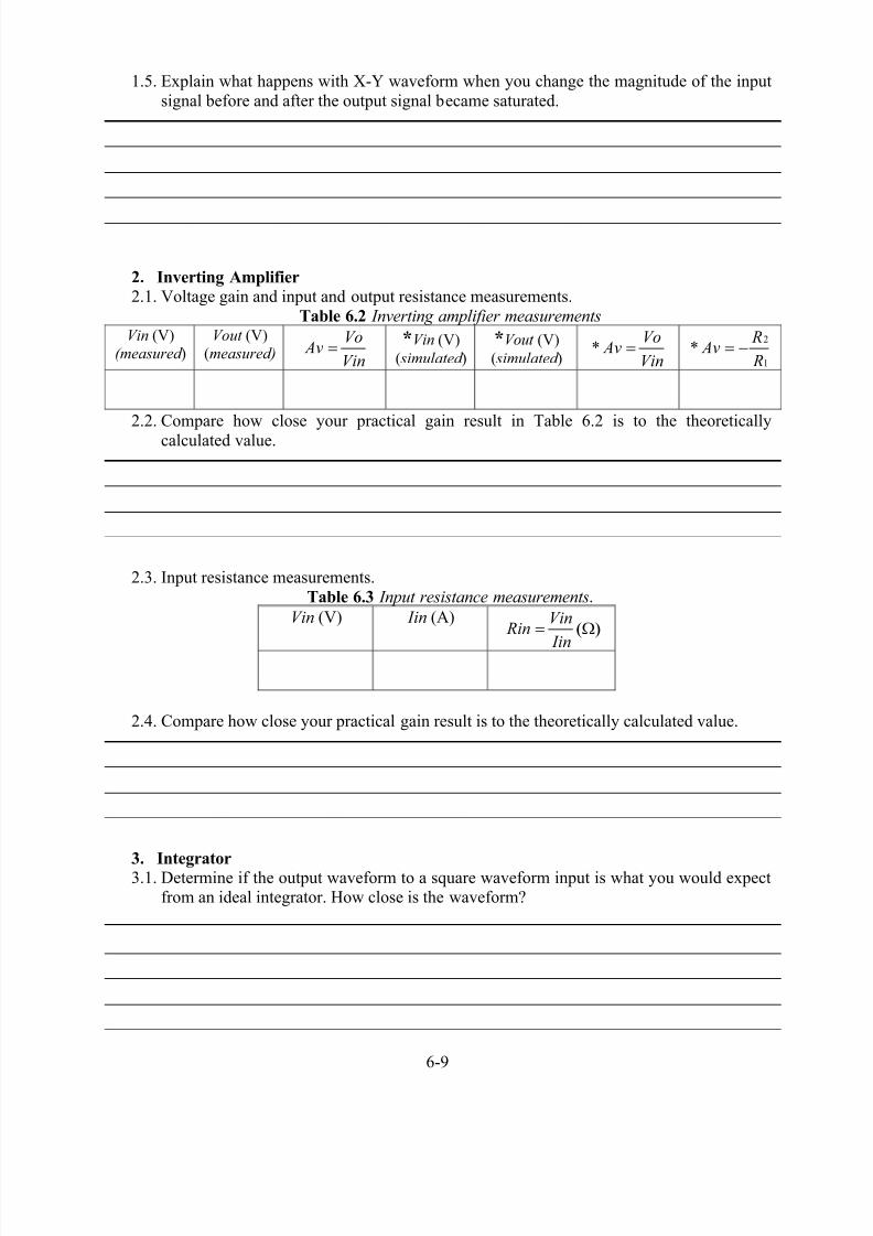
1.5. Explain what happens with X-Y waveform when you change the magnitude of the input
signal before and after the output signal became saturated.
2. Inverting Amplifier
2.1. Voltage gain and input and output resistance measurements.
Table 6.2 Inverting amplifier measurementsVin (V)
(measured )
Vout (V)
(measured)Vin
Vo Av =
*Vin (V)
( simulated )
*Vout (V)
( simulated ) Vin
Vo Av =*
1
2*
R
R Av -=
2.2. Compare how close your practical gain result in Table 6.2 is to the theoretically
calculated value.
2.3. Input resistance measurements.
Table 6.3 Input resistance measurements.
Vin (V) Iin (A)
Iin
Vin Rin = (W)
2.4. Compare how close your practical gain result is to the theoretically calculated value.
3. Integrator3.1. Determine if the output waveform to a square waveform input is what you would expectfrom an ideal integrator. How close is the waveform?

8/8/2019 26924074 Laboratory 6 Basic Op Amp Circuits
http://slidepdf.com/reader/full/26924074-laboratory-6-basic-op-amp-circuits 10/10
6-10
3.2. Draw the input and output waveforms of the integrator circuit for the triangle waveform
input signals.
a) Vin p-p = 0.4V b) Vin p-p = 2V
Figure 6.13 Triangle input signal waveforms
3.3. Determine if the output waveform is what you would expect from an ideal integrator.
How close is the waveform?
SIGNATURES TA name:________________________
To be completed by TA during the lab session.
Pre-lab completed.
Circuit in Figure 6.8 connected.
Circuit in Figure 6.9 connected.
Circuit in Figure 6.11 connected.
Data collected, questions attempted, lab submitted.
MARKSTo be completed by TA after the lab session.
Granted Marks Max. Marks Task
30 Pre-lab preparation
70 Data collection and answers
100 Total