Embed Size (px)
Citation preview
General DescriptionThe MAX3967A is a programmable LED driver for fiberoptic transmitters operating at data rates up to270Mbps. The circuit contains a high-speed current dri-ver with programmable temperature coefficient (temp-co), adjustments for LED prebias voltage, and a disablefeature. The circuit accepts PECL data inputs, andoperates from a single +2.97V to +5.5V power supply.
The SFP LED driver can switch up to 100mA into typicalhigh-speed light-emitting diodes. As temperatureincreases, the device’s modulation current increaseswith a tempco that is programmable from 2500ppm/°Cto 12,000ppm/°C. The modulation current is pro-grammed with a single external resistor.
The MAX3967A’s LED prebias voltage is programmablefrom 400mV to 925mV. The prebias circuit producespeaking current, which improves the LED switchingspeed.
Complementary current outputs help to maintain a con-stant supply current, reducing EMI and supply noisegenerated by the transmitter module. The MAX3967A isavailable in die form, or in a 4mm x 4mm, 24-pin thinQFN package.
ApplicationsMultimode LED Transmitters
Fast Ethernet/FDDI
155Mbps LAN ATM Transceivers
ESCON Receivers
SFP Transceivers
Features♦ TX_DISABLE for SFP Compatibility
♦ Single +2.97V to +5.5V Power Supply
♦ Adjustable Temperature Compensation
♦ Adjustable Modulation Current
♦ Complementary Output Reduces Supply Noise
♦ Programmable LED Prebias Voltage
♦ Available in 24-Pin Thin QFN or Die
MA
X3
96
7A
270Mbps SFP LED Driver
________________________________________________________________ Maxim Integrated Products 1
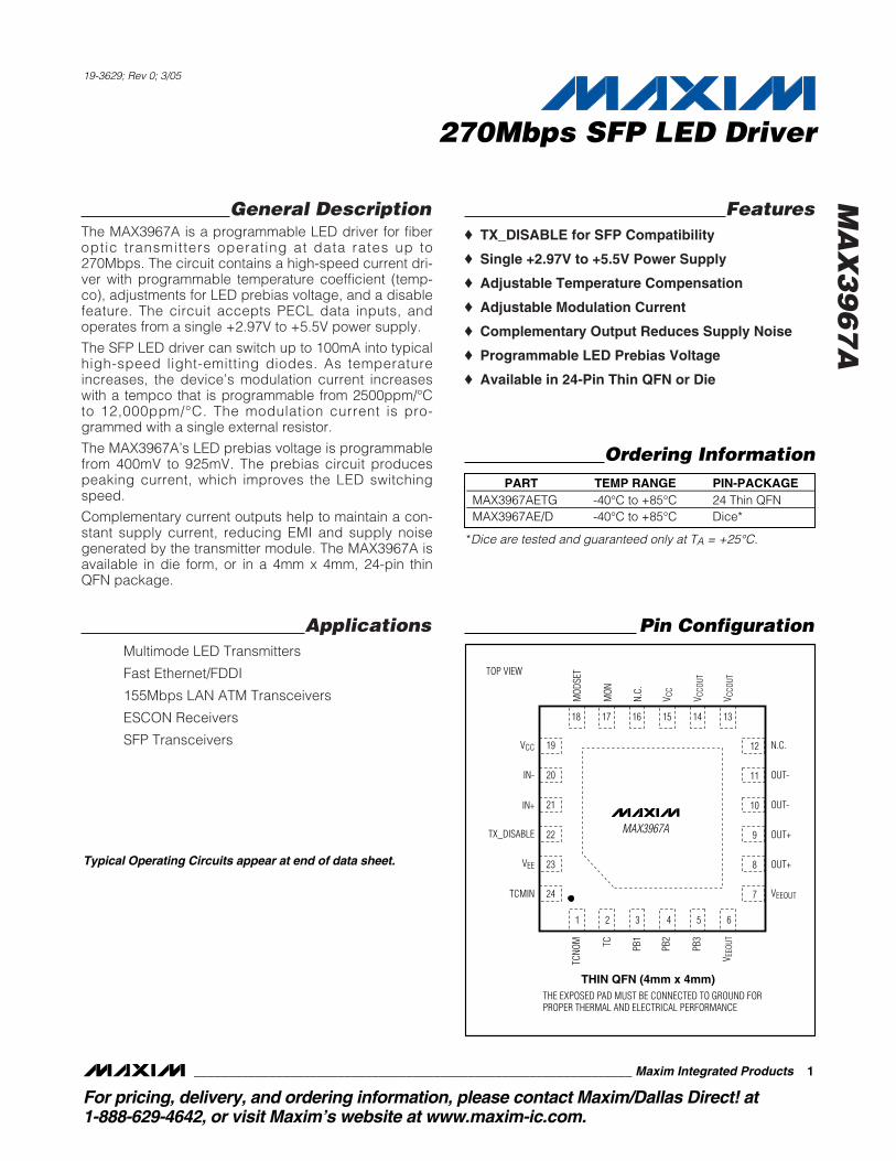
TOP VIEW
THE EXPOSED PAD MUST BE CONNECTED TO GROUND FORPROPER THERMAL AND ELECTRICAL PERFORMANCE
MAX3967A
THIN QFN (4mm x 4mm)
TCNO
M
1 2 3 4 5 6
7
8
9
10
11
12
131415161718
19
20
21
22
23
24
TC PB1
PB2
PB3
V EEO
UT
OUT+
OUT+
OUT-
N.C.
V CCO
UT
V CCO
UT
V CC
N.C.
MON
MOD
SET
IN-
IN+
VCC
VEE
TX_DISABLE
TCMIN VEEOUT
OUT-
Pin Configuration
19-3629; Rev 0; 3/05
For pricing, delivery, and ordering information, please contact Maxim/Dallas Direct! at 1-888-629-4642, or visit Maxim’s website at www.maxim-ic.com.
Ordering InformationPART TEMP RANGE PIN-PACKAGE
MAX3967AETG -40°C to +85°C 24 Thin QFNMAX3967AE/D -40°C to +85°C Dice*
Typical Operating Circuits appear at end of data sheet.
*Dice are tested and guaranteed only at TA = +25°C.
MA
X3
96
7A
270Mbps SFP LED Driver
2 _______________________________________________________________________________________
ABSOLUTE MAXIMUM RATINGSSupply Voltage at VCC, VCCOUT
(VEE, VEEOUT = 0V) ..............................................-0.5V to +7VCurrent into OUT+, OUT- ................................-40mA to +160mADifferential Output Voltage (OUT+ to OUT-) .........-3.3V to +3.3VVoltage at PB1, PB2, PB3,
IN+, IN-, OUT+, OUT-, TX_DISABLE......-0.5V to (VCC + 0.5V)Voltage at TCMIN, TCNOM, TC, MODSET, MON ....-0.5V to +2V
Continuous Power Dissipation (TA = +85°C)24-Lead Thin QFN (derate 20.8mW/C°above +85°C).............................................................1354mW
Operating Junction Temperature Range...........-40°C to +150°CDie Attach Temperature...................................................+375°CStorage Temperature Range .............................-50°C to +150°CLead Temperature (soldering, 10s) .................................+300°C
Stresses beyond those listed under “Absolute Maximum Ratings” may cause permanent damage to the device. These are stress ratings only, and functionaloperation of the device at these or any other conditions beyond those indicated in the operational sections of the specifications is not implied. Exposure toabsolute maximum rating conditions for extended periods may affect device reliability.
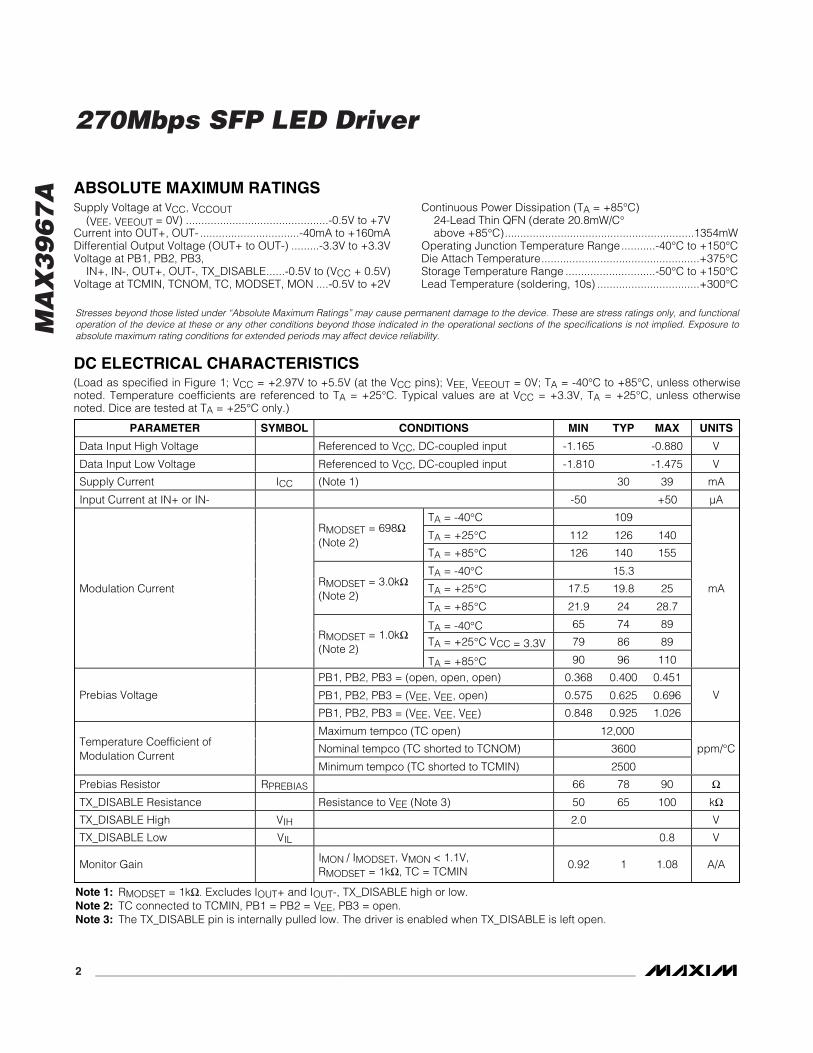
DC ELECTRICAL CHARACTERISTICS(Load as specified in Figure 1; VCC = +2.97V to +5.5V (at the VCC pins); VEE, VEEOUT = 0V; TA = -40°C to +85°C, unless otherwisenoted. Temperature coefficients are referenced to TA = +25°C. Typical values are at VCC = +3.3V, TA = +25°C, unless otherwisenoted. Dice are tested at TA = +25°C only.)
PARAMETER SYMBOL CONDITIONS MIN TYP MAX UNITS
Data Input High Voltage Referenced to VCC, DC-coupled input -1.165 -0.880 V
Data Input Low Voltage Referenced to VCC, DC-coupled input -1.810 -1.475 V
Supply Current ICC (Note 1) 30 39 mA
Input Current at IN+ or IN- -50 +50 µA
TA = -40°C 109
TA = +25°C 112 126 140RMODSET = 698Ω(Note 2)
TA = +85°C 126 140 155
TA = -40°C 15.3
TA = +25°C 17.5 19.8 25RMODSET = 3.0kΩ(Note 2)
TA = +85°C 21.9 24 28.7
TA = -40°C 65 74 89
TA = +25°C VCC = 3.3V 79 86 89
Modulation Current
RMODSET = 1.0kΩ(Note 2)
TA = +85°C 90 96 110
mA
PB1, PB2, PB3 = (open, open, open) 0.368 0.400 0.451
PB1, PB2, PB3 = (VEE, VEE, open) 0.575 0.625 0.696Prebias Voltage
PB1, PB2, PB3 = (VEE, VEE, VEE) 0.848 0.925 1.026
V
Maximum tempco (TC open) 12,000
Nominal tempco (TC shorted to TCNOM) 3600Temperature Coefficient ofModulation Current
Minimum tempco (TC shorted to TCMIN) 2500
ppm/°C
Prebias Resistor RPREBIAS 66 78 90 ΩTX_DISABLE Resistance Resistance to VEE (Note 3) 50 65 100 kΩTX_DISABLE High VIH 2.0 V
TX_DISABLE Low VIL 0.8 V
Monitor GainIMON / IMODSET, VMON < 1.1V,RMODSET = 1kΩ, TC = TCMIN
0.92 1 1.08 A/A
Note 1: RMODSET = 1kΩ. Excludes IOUT+ and IOUT-, TX_DISABLE high or low.Note 2: TC connected to TCMIN, PB1 = PB2 = VEE, PB3 = open.Note 3: The TX_DISABLE pin is internally pulled low. The driver is enabled when TX_DISABLE is left open.
MA
X3
96
7A
270Mbps SFP LED Driver
_______________________________________________________________________________________ 3
AC ELECTRICAL CHARACTERISTICS(Load as specified in Figure 1, unless otherwise noted. VCC = +2.97V to +5.5V (at the VCC pins), RMODSET = 1kΩ, TA = -40°C to+85°C. Input data shaped by 470MHz 4-pole filter, PB1 = PB2 = VEE, PB3 = open. Typical values are at VCC = +3.3V, TC connectedto TCMIN, TA = +25°C.) (Note 4)
PARAMETER SYMBOL CONDITIONS MIN TYP MAX UNITS
Data Input Range Differential input 500 2400 mVP-P
Output-Current Edge Speed 20% to 80%, input is a 12.5MHz square wave 300 615 1230 ps
Output-Current Pulse-WidthCorrection (PWC)
(Note 5) -90 ps
266Mbps (Note 6) 140Output-Current Data-DependentJitter
DJ155Mbps (Note 7) 150 250
psP-P
Random Jitter RJ 3 psRMS
TX_DISABLE Assert Time t_offTime from rising edge of TX_DISABLE tooutput at 10% of steady state
0.01 0.5 µs
TX_DISABLE Negate Time t_onTime from rising edge of TX_DISABLE tooutput at 90% of steady state
0.01 0.5 µs
Power-On Time t_initTime from VCC > 2.97V to output at 90% ofsteady state
0.1 2 ms
Figure 1. MAX3967A Output Test Loads
SWITCHING DIODE
OSCILLOSCOPE
OUT-
L1
OUT+
OUT+OUT-
AC ELECTRICAL LOADDC ELECTRICAL LOADFOR PREBIAS VOLTAGE
DC ELECTRICAL LOAD(EXCEPT PREBIAS VOLTAGE)
OUT+OUT-
MAX3967AMAX3967AMAX3967A
VCC
VCC
VLED1.55V
50Ω
5Ω
50Ω
0.22µF
0.22µF
FERRITEBEAD
VCC
VPREBIAS
Note 4: AC characteristics are guaranteed by design and characterization.Note 5: PWC = (widthCURRENT ON - widthCURRENT OFF) / 2.Note 6: Test pattern is a K28.5 (0011 1110 1011 0000 0101) transmitted at 266Mbps.Note 7: Test pattern is equivalent to a 213 - 1 PRBS containing 72 consecutive zeros or 72 consecutive ones.
MA
X3
96
7A
270Mbps SFP LED Driver
4 _______________________________________________________________________________________
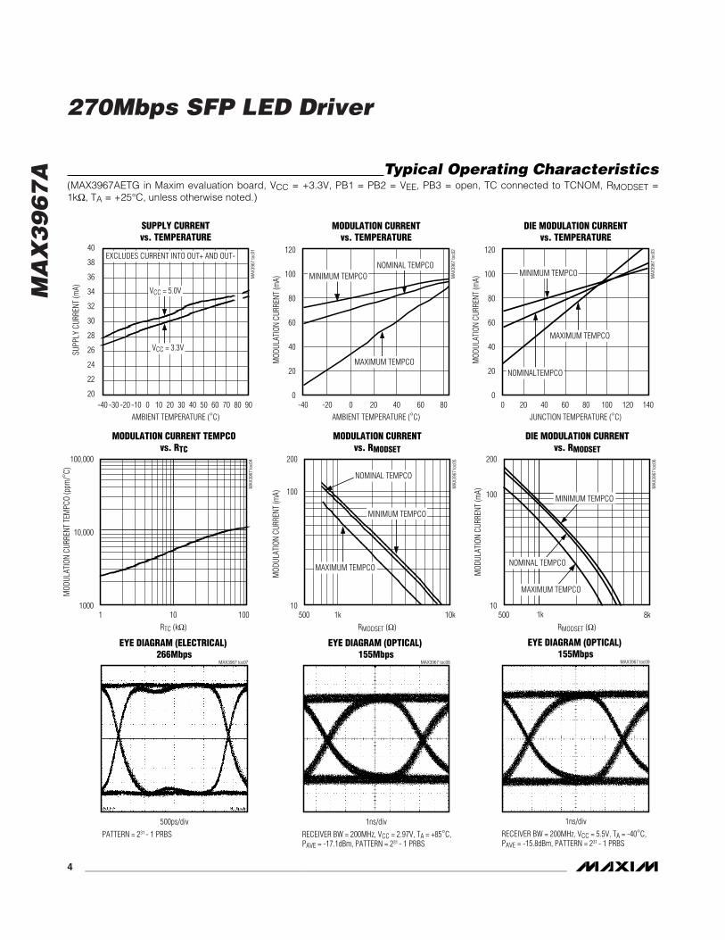
Typical Operating Characteristics(MAX3967AETG in Maxim evaluation board, VCC = +3.3V, PB1 = PB2 = VEE, PB3 = open, TC connected to TCNOM, RMODSET =1kΩ, TA = +25°C, unless otherwise noted.)
40
38
36
34
32
30
28
26
24
22
20-40 -20 -10-30 0 10 20 30 40 50 60 70 80 90
SUPPLY CURRENTvs. TEMPERATURE
MAX
3967
toc0
1
AMBIENT TEMPERATURE (°C)
SUPP
LY C
URRE
NT (m
A)
EXCLUDES CURRENT INTO OUT+ AND OUT-
VCC = 5.0V
VCC = 3.3V
0
40
20
80
60
100
120
-40 20 40-20 0 60 80
MODULATION CURRENTvs. TEMPERATURE
MAX
3967
toc0
2
AMBIENT TEMPERATURE (°C)
MOD
ULAT
ION
CURR
ENT
(mA) MINIMUM TEMPCO
NOMINAL TEMPCO
MAXIMUM TEMPCO
0
40
20
80
60
100
120
0 60 8020 40 100 120 140
DIE MODULATION CURRENTvs. TEMPERATURE
MAX
3967
toc0
3
JUNCTION TEMPERATURE (°C)
MOD
ULAT
ION
CURR
ENT
(mA)
MINIMUM TEMPCO
NOMINALTEMPCO
MAXIMUM TEMPCO
100,000
10001 10 100
MODULATION CURRENT TEMPCOvs. RTC
MAX
3967
toc0
4
RTC (kΩ)
MOD
ULAT
ION
CURR
ENT
TEM
PCO
(ppm
/°C)
10,000
200
10500 1k 10k
MODULATION CURRENTvs. RMODSET
MAX
3967
toc0
5
RMODSET (Ω)
MOD
ULAT
ION
CURR
ENT
(mA) 100
MINIMUM TEMPCO
NOMINAL TEMPCO
MAXIMUM TEMPCO
200
10500 1k 8k
DIE MODULATION CURRENTvs. RMODSET
MAX
3967
toc0
6
RMODSET (Ω)
MOD
ULAT
ION
CURR
ENT
(mA) 100
MAXIMUM TEMPCO
NOMINAL TEMPCO
MINIMUM TEMPCO
EYE DIAGRAM (ELECTRICAL) 266Mbps
MAX3967 toc07
500ps/div
PATTERN = 231 - 1 PRBS
EYE DIAGRAM (OPTICAL) 155Mbps
MAX3967 toc08
1ns/div
RECEIVER BW = 200MHz, VCC = 2.97V, TA = +85°C, PAVE = -17.1dBm, PATTERN = 231 - 1 PRBS
EYE DIAGRAM (OPTICAL) 155Mbps
MAX3967 toc09
1ns/div
RECEIVER BW = 200MHz, VCC = 5.5V, TA = -40°C, PAVE = -15.8dBm, PATTERN = 231 - 1 PRBS
MA
X3
96
7A
270Mbps SFP LED Driver
_______________________________________________________________________________________ 5
EYE DIAGRAM (OPTICAL) 155Mbps
MAX3967 toc10
1ns/div
RECEIVER BW = 200MHz, VCC = 5.5V, TA = +85°C, PAVE = -17.1dBm, PATTERN = 231 - 1 PRBS
EYE DIAGRAM (OPTICAL) 155Mbps
MAX3967 toc11
1ns/div
RECEIVER BW = 200MHz, VCC = 2.97V, TA = -40°C, PAVE = -15.8dBm, PATTERN = 231 - 1 PRBS
0
2
1
4
3
5
6
0 10 20 30 40 50 60 70 80 90
RANDOM JITTERvs. TEMPERATURE
MAX
3967
toc1
2
AMBIENT TEMPERATURE (°C)
RAND
OM JI
TTER
(ps R
MS)
VCC = 5.0VMINIMUM TEMPCO
VCC = 3.3VMAXIMUM TEMPCO
TX_DISABLE NEGATE TIMEMAX3967 toc13
4ns/div
LEDOUTPUT
TX_DISABLE
t_on
TX_DISABLE ASSERT TIMEMAX3967 toc14
4ns/div
LEDOUTPUT
TX_DISABLE
t_off
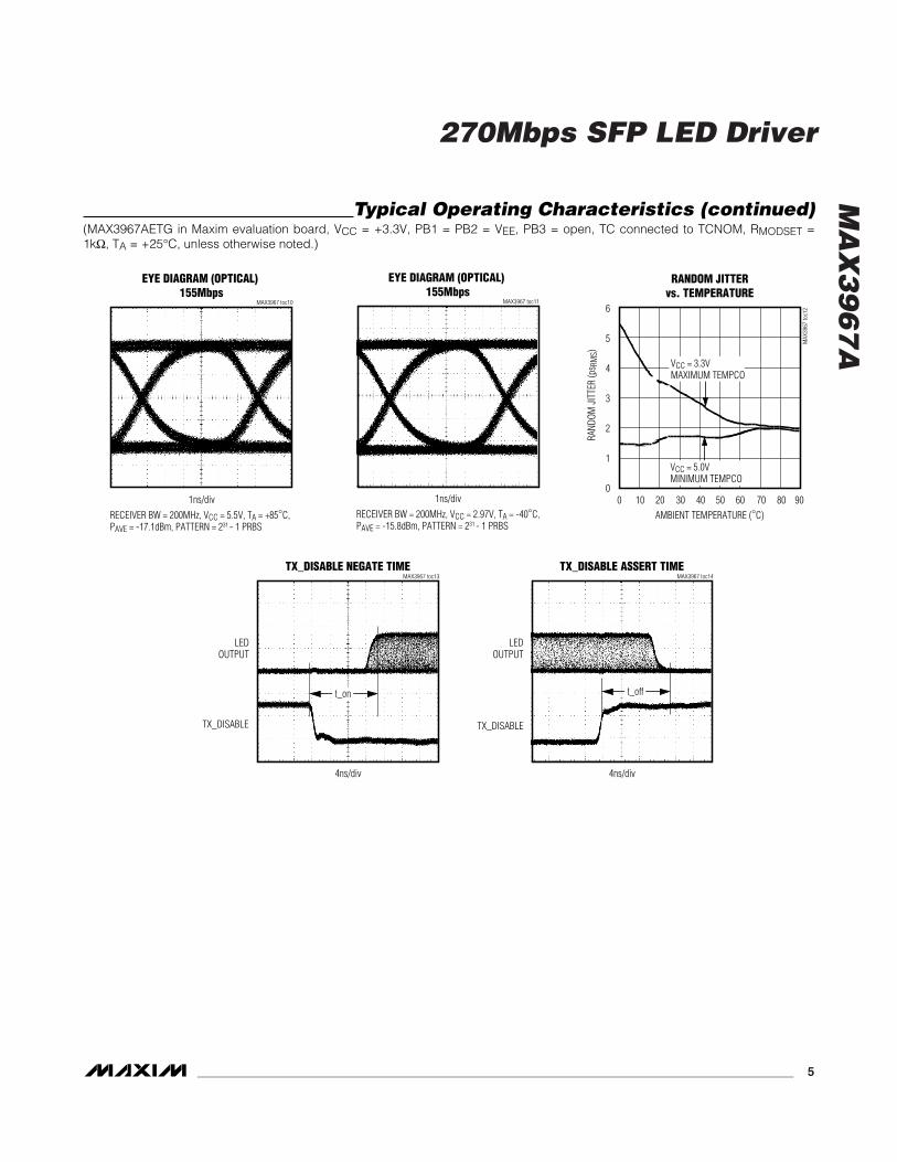
Typical Operating Characteristics (continued)(MAX3967AETG in Maxim evaluation board, VCC = +3.3V, PB1 = PB2 = VEE, PB3 = open, TC connected to TCNOM, RMODSET =1kΩ, TA = +25°C, unless otherwise noted.)
MA
X3
96
7A
Detailed DescriptionThe MAX3967A provides a flexible current drive for themodulation of fiber optic light-emitting diodes (LEDs).The circuit is designed to be used with +3.3V or +5Vpower supplies. The IC provides up to 100mA of modu-lation current. An adjustable prebias current source setsthe LED prebias voltage. An integrated resistor providespassive peaking and optical pulse-width compensation.
Figure 2 shows a block diagram of the MAX3967A,which comprises a reference-voltage generator, modu-lation-current generator, input buffer with disable, pre-bias-current generator, main output driver,complementary output driver, and LED-compensationnetwork.
Temperature CompensationThe reference-voltage generator circuit provides twovoltage sources that create modulation-current tempera-ture compensation. A positive modulation-current tem-
perature coefficient (tempco) is useful to compensatefor the temperature characteristics of typical fiber opticLEDs. The first source has a temperature-stable output.The second source has a temperature-increasing outputwith a tempco of approximately 12,000ppm/°C (relativeto +25°C). A resistor-divider between the two referencegenerators programs the modulation-current tempco.For maximum modulation-current tempco, leave the TCpin disconnected. For a tempco of approximately3600ppm/°C, connect TC to TCNOM. To obtain the mini-mum tempco, connect TCMIN to TC. Intermediate temp-co values can be programmed by connecting anexternal resistor (RTC) between TCMIN and TC.
Input BufferThe inputs are connected to the PECL-compatible differ-ential input buffer. If left unconnected, IN+ is internallypulled to a PECL low and IN- is pulled to a PECL high,causing low current at OUT+. The input impedance ofIN+ and IN- is approximately 50kΩ.
270Mbps SFP LED Driver
6 _______________________________________________________________________________________
PIN NAME FUNCTION
1 TCNOM Shorting TC to TCNOM provides a modulation tempco of approximately 3600ppm/°C.
2 TCA resistor (RTC) connected between the TC and TCMIN pins sets the tempco of the modulationcurrent. Leaving RTC unconnected provides the maximum tempco.
3, 4, 5 PB1, PB2, PB3 Programs the Prebias Voltage at the OUT+ Pin (Table 1)
6, 7 VEEOUT Ground for the Output-Current Drivers
8, 9 OUT+ Current Output
10, 11 OUT- Complementary Current Output
12, 16 N.C. No Connection. Not internally connected.
13, 14 VCCOUT Supply Connection for the Output-Current Drivers
15, 19 VCC Provides Current to the Internal Amplifiers
17 MON The Current Sourced from the MON Pin is Proportional to the Modulator Current
18 MODSET A Resistor from MODSET to VEE Programs the LED Modulation Current
20 IN- Inverting Data Input
21 IN+ Noninverting Data Input
22 TX_DISABLETransmit Disable. When high, the current at the OUT+ pins is in the low state. The transmitter isenabled when TX_DISABLE is open.
23 VEE Ground for internal amplifiers.
24 TCMIN Shorting TC to TCMIN provides the minimum modulation-current tempco.
EP Exposed Pad Connect the exposed pad to board ground for optimal correct electrical and thermal performance.
Pin Description
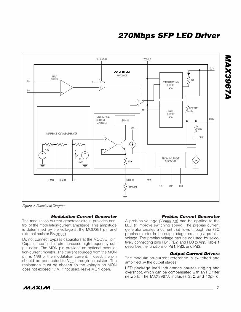
Modulation-Current GeneratorThe modulation-current generator circuit provides con-trol of the modulation-current amplitude. This amplitudeis determined by the voltage at the MODSET pin andexternal resistor RMODSET.
Do not connect bypass capacitors at the MODSET pin.Capacitance at this pin increases high-frequency out-put noise. The MON pin provides an optional modula-tion-current monitor. The current sourced from the MONpin is 1/96 of the modulation current. If used, the pinshould be connected to VEE through a resistor. Theresistance must be chosen so the voltage on MONdoes not exceed 1.1V. If not used, leave MON open.
Prebias Current GeneratorA prebias voltage (VPREBIAS) can be applied to the LED to improve switching speed. The prebias currentgenerator creates a current that flows through the 78Ωprebias resistor in the output stage, creating a prebiasvoltage. The prebias voltage can be adjusted by selec-tively connecting pins PB1, PB2, and PB3 to VEE. Table 1describes the functions of PB1, PB2, and PB3.
Output Current DriversThe modulation-current reference is switched andamplified by the output stages.
LED package lead inductance causes ringing andovershoot, which can be compensated with an RC filternetwork. The MAX3967A includes 35Ω and 12pF of
MA
X3
96
7A
270Mbps SFP LED Driver
_______________________________________________________________________________________ 7
Figure 2. Functional Diagram
12pF
MODULATION-CURRENTGENERATOR
REFERENCE-VOLTAGE GENERATOR
PREBIAS-CURRENTGENERATOR
COMPLEMENTARYOUTPUT
24X
MAINOUTPUT
24X
V
TEMP
TCMIN
PB1 PB2 PB3
TCNOM TC MODSET MON
1.2V
OUT-
OUT+
IN-
IN+
INPUTBUFFER
GAIN 4X
MAX3967A
RMODSET
VCCOUTTX_DISABLE
50Ω
35Ω
5Ω
VCC
RPREBIAS78Ω
10
0
MA
X3
96
7A
internal compensation. The compensation network canbe optimized by adding additional componentsbetween VCCOUT and OUT+.
The MAX3967A includes a complementary output dri-ver, which is switched 180° out of phase with the mainoutput. This configuration helps to maintain constantcurrent flow from the voltage supply, reducing noiseand EMI. A large diode and a 5Ω resistor are connect-ed in series with the negative output (OUT-) to emulatethe LED load at OUT+.
Peaking CurrentThe prebias resistor provides peaking current to improvethe LED switching speed. The peaking magnitude isgiven by the following equation:
The peaking amplitude is equal for rising and fallingdata transitions.
Design ProcedureSelect an LED
For best performance, select a high-efficiency, low-inductance LED. LED inductance causes large voltageswings and ringing.
Program the Modulation-Current TempcoSelect a modulation-current tempco that provides near-ly constant LED output power as temperature varies.For the minimum tempco, connect TCMIN to the TC pin.For a tempco of approximately 3600ppm/°C, connectTC to TCNOM and leave TCMIN unconnected. For themaximum tempco, leave TCMIN, TCNOM, and TCunconnected.
See the Modulation Current Tempco vs. RTC graph inthe Typical Operating Characteristics to program a cus-tom tempco. From the graph, determine the appropriateresistor and connect it between TCMIN and TC.
For example, if an LED requires a 5000ppm/°C tempco,choose RTC of 8.3kΩ.
Program the Modulation CurrentDetermine the required modulation current at TA = +25°C.Then select the appropriate value of RMODSET from theModulation Current vs. RMODSET graph in the TypicalOperating Characteristics.
For example, to program 75mA modulation current, thegraph indicates an RMODSET value of 750Ω for maxi-mum tempco (12,000ppm/°C) and 1kΩ for nominaltempco (3600ppm/°C). By interpolation, choose anRMODSET of 792Ω for a tempco of 5000ppm/°C.
Program Prebias VoltageDetermine the LED prebias voltage that produces anacceptable trade-off between peaking current and extinc-tion ratio. See Table 1 for PB1, PB2, and PB3 settings.
Layout ConsiderationsFor optimum performance, total load inductance shouldnot exceed 10nH. Load inductance includes LEDinductance, LED package lead inductance, and circuit-board traces. Keep the connections between theMAX3967A OUT pins and the LED as short as possibleto minimize inductance.
Chip-and-wire (hybrid) technology reduces packageinductance significantly, and provides the best possibleperformance.
Use good high-frequency layout techniques and a multilayer board with an uninterrupted ground plane.Power supplies should be capacitively bypassed to theground plane with surface-mount capacitors locatednear the power-supply pins.
IPEAKLED PREBIASV -V
78=
Ω
270Mbps SFP LED Driver
8 _______________________________________________________________________________________
Table 1. LED Prebias Voltage
PB1 PB2 PB3 PREBIAS (V)
Open Open Open 0.400
VEE Open Open 0.475
Open VEE Open 0.550
VEE VEE Open 0.625
Open Open VEE 0.700
VEE Open VEE 0.775
Open VEE VEE 0.850
VEE VEE VEE 0.925
Applications InformationWire-Bonding Die
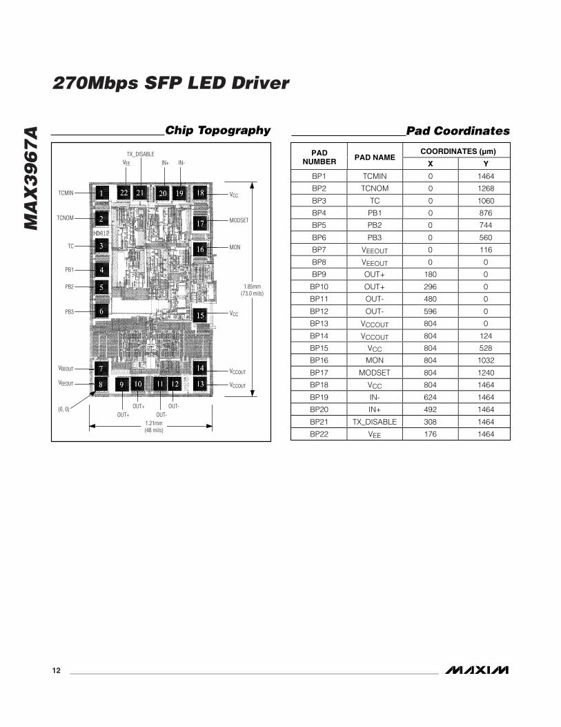
The MAX3967A utilizes gold metalization, which pro-vides high reliability. Make connections to the die withgold wire only, using ball-bonding techniques. Usecaution if attempting wedge-bonding. Pad size is 4 milsx 4 mils (100µm). Die thickness is typically 15 mils(375µm).
Exposed-Pad PackageThe exposed pad on the 24-pin TQFN provides a verylow thermal resistance path for heat removal from the IC.
Chip InformationTRANSISTOR COUNT: 331
SUBSTRATE CONNECTED TO VEE
PROCESS: BIPOLAR
DIE THICKNESS: 15 mils
MA
X3
96
7A
270Mbps SFP LED Driver
_______________________________________________________________________________________ 9
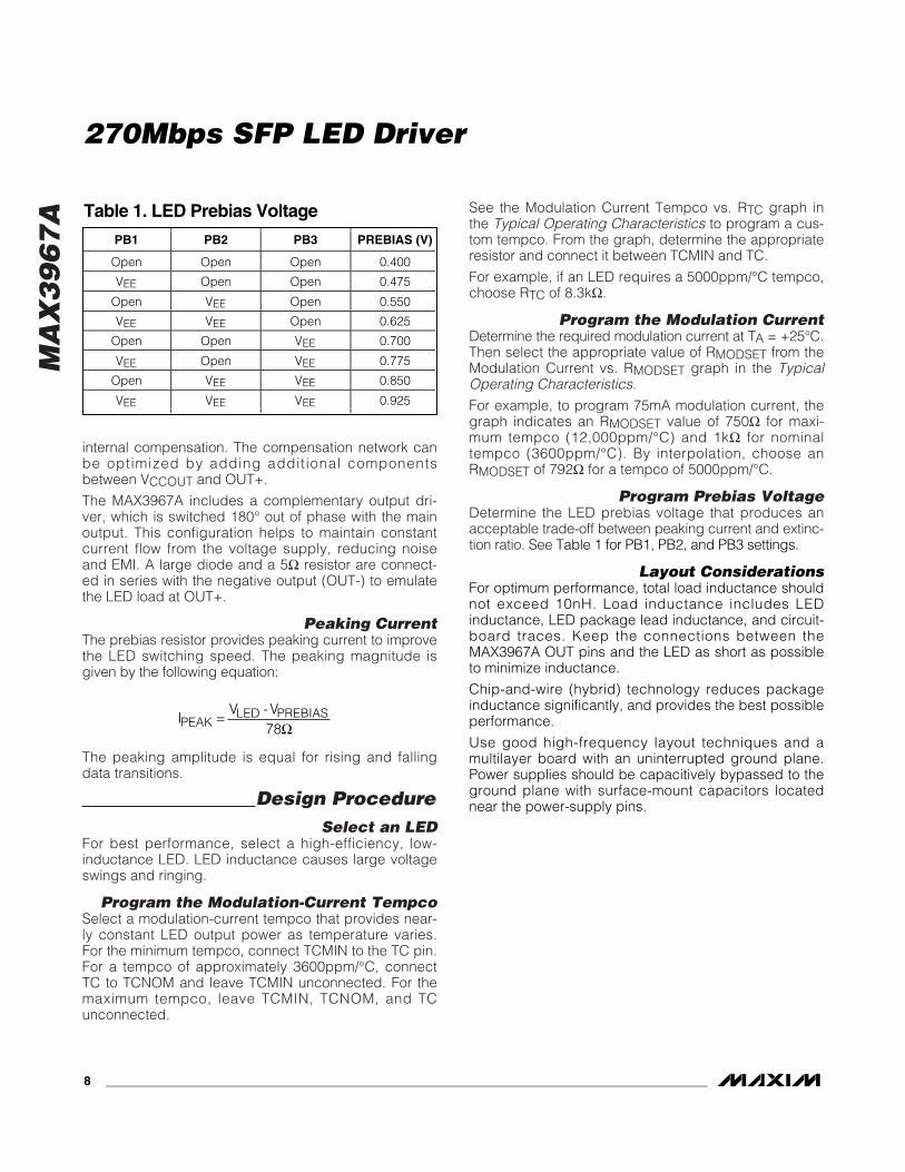
Input Terminations
PECLOUTPUT IN+
VCC
VCC
VCC - 2V
50Ω
3.3 82 130
R1 R2
5.0 68 180
R1
R2
RF OR NON-PECLOUTPUT
IN+
SINGLE-ENDED TERMINATION IS SHOWN. IN- SHOULD BE TERMINATED SIMILARLY.
MAX3967A
MAX3967A
Figure 3. Input Terminations
MA
X3
96
7A
270Mbps SFP LED Driver
10 ______________________________________________________________________________________
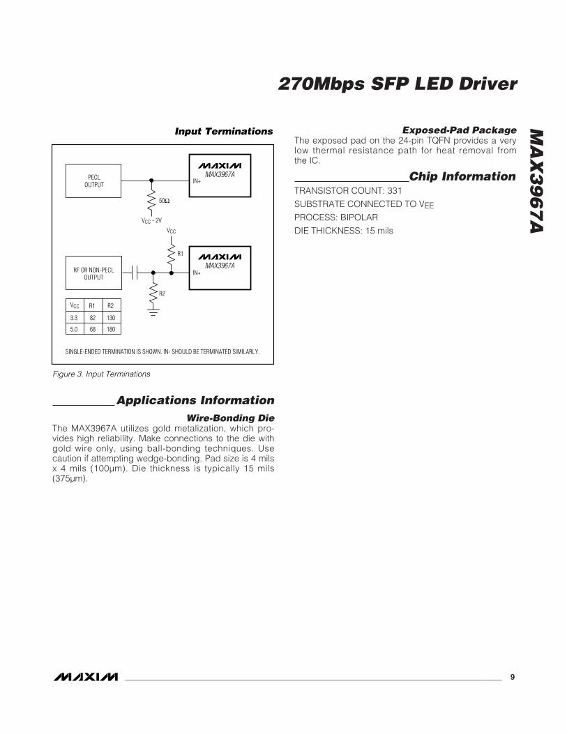
MODSETTCTCNOM
TX_DISABLEDISABLE
PB3PB2PB1
IN-
MON
IN+
FERRITE BEAD
MAX3967A
10kΩ
VEEOUT
CIN
VCCOUTVCC
RMODSET
RMON
OUT+
OUT-
VEE
+3.3V
SFP TRANSMITTER WITH DIGITAL MONITOR
82Ω
+3.3V
120Ω
82Ω
+3.3V
120Ω
CIN
DIAGNOSTICIC
DIFFERENTIALDATA
TCMIN
MODSETTCTCMIN
TX_DISABLEDISABLE
DIFFERENTIALDATA
PB3PB2PB1
IN-
IN+
FERRITE BEAD
MAX3967A
10kΩ
VEEOUT
CIN
VCCOUTVCC
RMODSET
OUT+
OUT-
VEE
+3.3V
SFP TRANSMITTER
82Ω
+3.3V
120Ω
82Ω
+3.3V
120Ω
CIN TCNOM
Typical Operating Circuits
MA
X3
96
7A
270Mbps SFP LED Driver
______________________________________________________________________________________ 11
MODSETTC
RTC*
TCNOM TCMIN
TX_DISABLE
*OPTIONAL COMPONENT
DISABLE
PECLDATA
PB3PB2PB1
IN-
MON
IN+
FERRITE BEAD
MAX3967A
VEEOUT
VCCOUTVCC
RMODSET
OUT+
OUT-
VEE
VCC
SFF TRANSMITTER WITH DISABLE
Typical Operating Circuits (continued)
MODSETTCTCMINTCNOM
TX_DISABLE
PECLDATA
PB3PB2PB1
IN-
IN+
FERRITE BEAD
MAX3967A
VEEOUT
VCCOUTVCC
RMODSET
OUT+
OUT-
VEE
VCC
SFF TRANSMITTER WITHOUT DISABLE
MON
MA
X3
96
7A
270Mbps SFP LED Driver
12 ______________________________________________________________________________________
TCMIN
TCNOM
TC
PB1
PB2
PB3
OUT+OUT+
OUT-OUT-
MON
MODSET
IN-IN+TX_DISABLE
1.21mm(48 mils)
(0, 0)
1.85mm(73.0 mils)
VCC
VCC
VCCOUTVEEOUT
VEEOUT VCCOUT
VEE
Chip Topography Pad Coordinates
COORDINATES (µm)PADNUMBER PAD NAME
X Y
BP1 TCMIN 0 1464
BP2 TCNOM 0 1268
BP3 TC 0 1060
BP4 PB1 0 876
BP5 PB2 0 744
BP6 PB3 0 560
BP7 VEEOUT 0 116
BP8 VEEOUT 0 0
BP9 OUT+ 180 0
BP10 OUT+ 296 0
BP11 OUT- 480 0
BP12 OUT- 596 0
BP13 VCCOUT 804 0
BP14 VCCOUT 804 124
BP15 VCC 804 528
BP16 MON 804 1032
BP17 MODSET 804 1240
BP18 VCC 804 1464
BP19 IN- 624 1464
BP20 IN+ 492 1464
BP21 TX_DISABLE 308 1464
BP22 VEE 176 1464
MA
X3
96
7A
270Mbps SFP LED Driver
______________________________________________________________________________________ 13
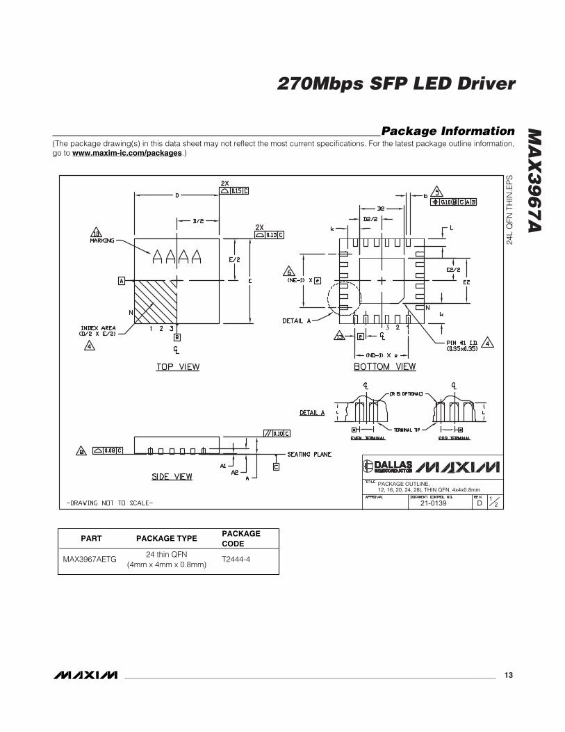
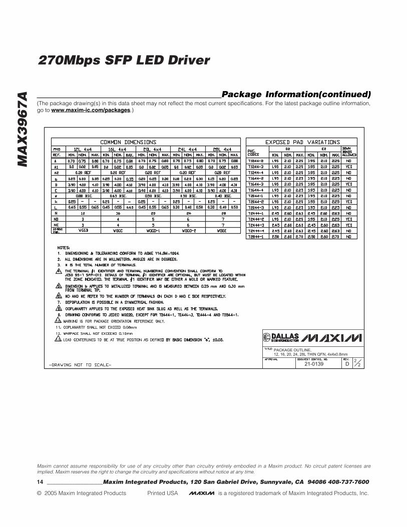
Package Information(The package drawing(s) in this data sheet may not reflect the most current specifications. For the latest package outline information,go to www.maxim-ic.com/packages.)
24L
QFN
TH
IN.E
PS
PACKAGE OUTLINE,
21-0139 21
D
12, 16, 20, 24, 28L THIN QFN, 4x4x0.8mm
PART PACKAGE TYPEPACKAGECODE
MAX3967AETG24 thin QFN
(4mm x 4mm x 0.8mm)T2444-4
MA
X3
96
7A
270Mbps SFP LED Driver
Maxim cannot assume responsibility for use of any circuitry other than circuitry entirely embodied in a Maxim product. No circuit patent licenses areimplied. Maxim reserves the right to change the circuitry and specifications without notice at any time.
14 ____________________Maxim Integrated Products, 120 San Gabriel Drive, Sunnyvale, CA 94086 408-737-7600
© 2005 Maxim Integrated Products Printed USA is a registered trademark of Maxim Integrated Products, Inc.
Package Information(continued)(The package drawing(s) in this data sheet may not reflect the most current specifications. For the latest package outline information,go to www.maxim-ic.com/packages.)
PACKAGE OUTLINE,
21-0139 22
D
12, 16, 20, 24, 28L THIN QFN, 4x4x0.8mm