Embed Size (px)
Citation preview
280 IEEE TRANSACTIONS ON ADVANCED PACKAGING, VOL. 32, NO. 2, MAY 2009
Predicting Microwave Digital Signal IntegrityJames F. Buckwalter, Member, IEEE
Abstract—High-speed digital signal integrity at data rates above6 Gb/s is an obstacle to reliable serial link operation. Two signalintegrity challenges include dispersion due to frequency-depen-dent losses and reflections created at impedance mismatches.Signal integrity analysis relies on time-domain simulation ofpseudo-random data patterns. This paper explores a predictivemethod for interconnect eye closure caused by reflections at thetransmitter and receiver and does not require extensive time do-main simulation. Worst-case bounds on intersymbol interferenceand data-dependent jitter aid prediction for link budgets underchannel variations. This method is applied to the design of apassive equalizer.
Index Terms—Data dependent jitter, interconnect modeling, in-tersymbol interference, jitter, signal integrity.
I. INTRODUCTION
D IGITAL signal integrity analysis is necessary for seriallinks operating over 6 Gb/s. Microwave digital signals
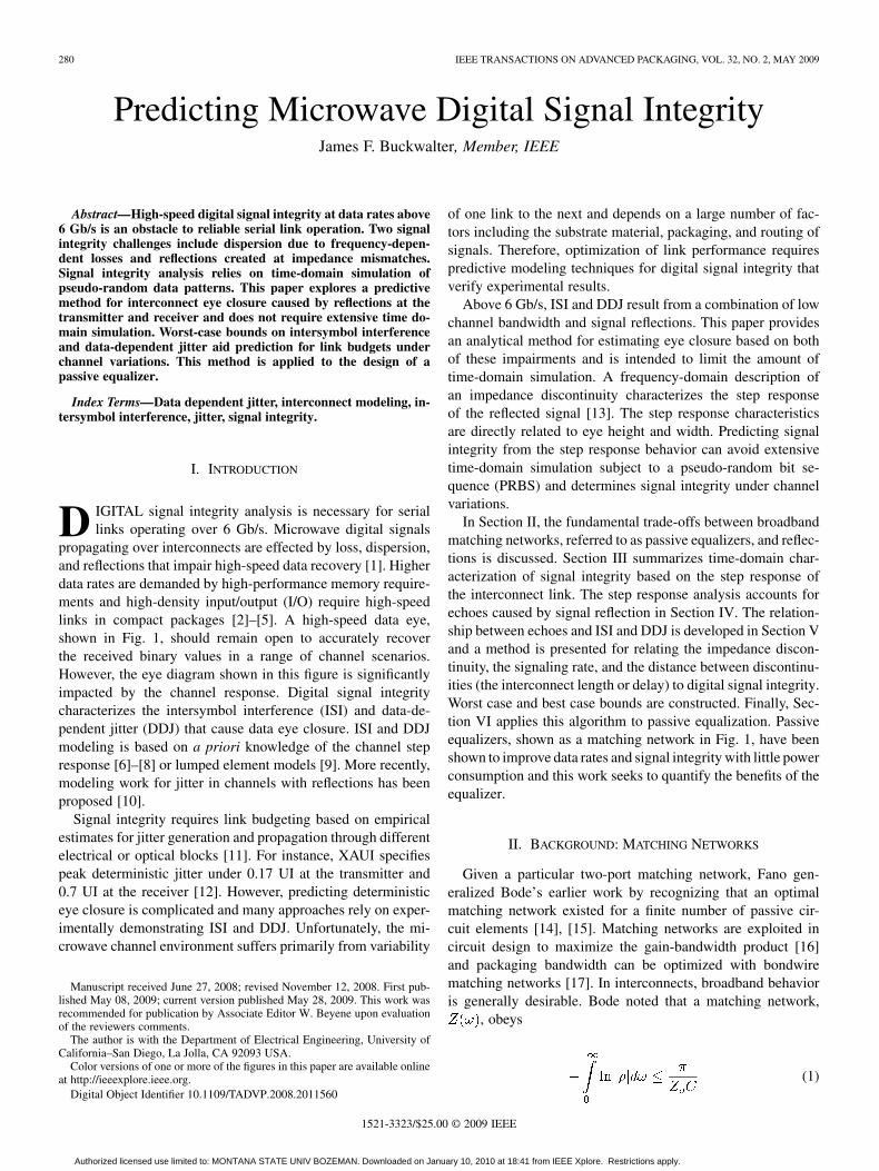
propagating over interconnects are effected by loss, dispersion,and reflections that impair high-speed data recovery [1]. Higherdata rates are demanded by high-performance memory require-ments and high-density input/output (I/O) require high-speedlinks in compact packages [2]–[5]. A high-speed data eye,shown in Fig. 1, should remain open to accurately recoverthe received binary values in a range of channel scenarios.However, the eye diagram shown in this figure is significantlyimpacted by the channel response. Digital signal integritycharacterizes the intersymbol interference (ISI) and data-de-pendent jitter (DDJ) that cause data eye closure. ISI and DDJmodeling is based on a priori knowledge of the channel stepresponse [6]–[8] or lumped element models [9]. More recently,modeling work for jitter in channels with reflections has beenproposed [10].
Signal integrity requires link budgeting based on empiricalestimates for jitter generation and propagation through differentelectrical or optical blocks [11]. For instance, XAUI specifiespeak deterministic jitter under 0.17 UI at the transmitter and0.7 UI at the receiver [12]. However, predicting deterministiceye closure is complicated and many approaches rely on exper-imentally demonstrating ISI and DDJ. Unfortunately, the mi-crowave channel environment suffers primarily from variability
Manuscript received June 27, 2008; revised November 12, 2008. First pub-lished May 08, 2009; current version published May 28, 2009. This work wasrecommended for publication by Associate Editor W. Beyene upon evaluationof the reviewers comments.
The author is with the Department of Electrical Engineering, University ofCalifornia–San Diego, La Jolla, CA 92093 USA.
Color versions of one or more of the figures in this paper are available onlineat http://ieeexplore.ieee.org.
Digital Object Identifier 10.1109/TADVP.2008.2011560
of one link to the next and depends on a large number of fac-tors including the substrate material, packaging, and routing ofsignals. Therefore, optimization of link performance requirespredictive modeling techniques for digital signal integrity thatverify experimental results.
Above 6 Gb/s, ISI and DDJ result from a combination of lowchannel bandwidth and signal reflections. This paper providesan analytical method for estimating eye closure based on bothof these impairments and is intended to limit the amount oftime-domain simulation. A frequency-domain description ofan impedance discontinuity characterizes the step responseof the reflected signal [13]. The step response characteristicsare directly related to eye height and width. Predicting signalintegrity from the step response behavior can avoid extensivetime-domain simulation subject to a pseudo-random bit se-quence (PRBS) and determines signal integrity under channelvariations.
In Section II, the fundamental trade-offs between broadbandmatching networks, referred to as passive equalizers, and reflec-tions is discussed. Section III summarizes time-domain char-acterization of signal integrity based on the step response ofthe interconnect link. The step response analysis accounts forechoes caused by signal reflection in Section IV. The relation-ship between echoes and ISI and DDJ is developed in Section Vand a method is presented for relating the impedance discon-tinuity, the signaling rate, and the distance between discontinu-ities (the interconnect length or delay) to digital signal integrity.Worst case and best case bounds are constructed. Finally, Sec-tion VI applies this algorithm to passive equalization. Passiveequalizers, shown as a matching network in Fig. 1, have beenshown to improve data rates and signal integrity with little powerconsumption and this work seeks to quantify the benefits of theequalizer.
II. BACKGROUND: MATCHING NETWORKS
Given a particular two-port matching network, Fano gen-eralized Bode’s earlier work by recognizing that an optimalmatching network existed for a finite number of passive cir-cuit elements [14], [15]. Matching networks are exploited incircuit design to maximize the gain-bandwidth product [16]and packaging bandwidth can be optimized with bondwirematching networks [17]. In interconnects, broadband behavioris generally desirable. Bode noted that a matching network,
, obeys
(1)
1521-3323/$25.00 © 2009 IEEE
Authorized licensed use limited to: MONTANA STATE UNIV BOZEMAN. Downloaded on January 10, 2010 at 18:41 from IEEE Xplore. Restrictions apply.
BUCKWALTER: PREDICTING MICROWAVE DIGITAL SIGNAL INTEGRITY 281
Fig. 1. Example of a high-speed interconnect with passive equalization net-works for improved digital signal integrity with a 6 Gb/s data eye.
where is the reflection coefficient between the matching net-work and the interconnect
(2)
In other words, the low-frequency channel impedance and high-frequency susceptance determine the achievable channel band-width. The limit in (1) exists for the product of the reflectioncoefficient and the bandwidth. In other words, increasing thetolerance for reflections increases the channel bandwidth. Thisinsight motivates understanding the trade-off of bandwidth andreflection for digital signal integrity.
Consider a transmission line termination, , and capaci-tance, . Approximating the integral in (1) with a bound on theacceptable reflection coefficient, ,also bounds the bandwidth, BW
(3)
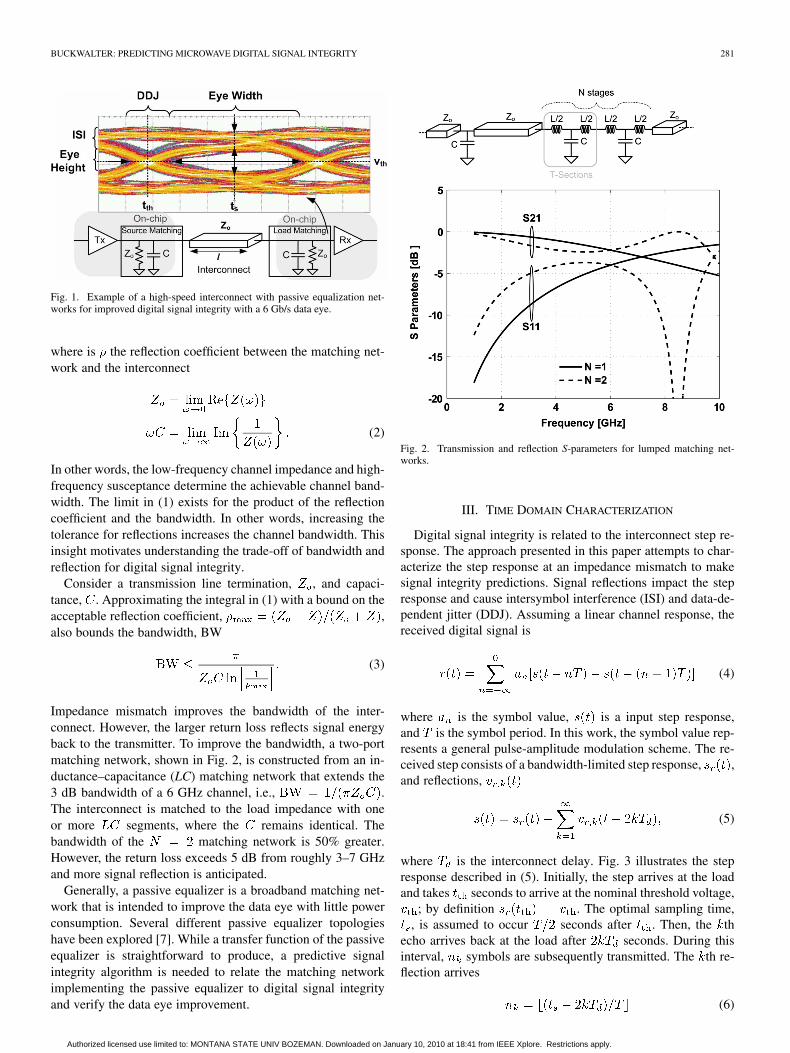
Impedance mismatch improves the bandwidth of the inter-connect. However, the larger return loss reflects signal energyback to the transmitter. To improve the bandwidth, a two-portmatching network, shown in Fig. 2, is constructed from an in-ductance–capacitance (LC) matching network that extends the3 dB bandwidth of a 6 GHz channel, i.e., .The interconnect is matched to the load impedance with oneor more segments, where the remains identical. Thebandwidth of the matching network is 50% greater.However, the return loss exceeds 5 dB from roughly 3–7 GHzand more signal reflection is anticipated.
Generally, a passive equalizer is a broadband matching net-work that is intended to improve the data eye with little powerconsumption. Several different passive equalizer topologieshave been explored [7]. While a transfer function of the passiveequalizer is straightforward to produce, a predictive signalintegrity algorithm is needed to relate the matching networkimplementing the passive equalizer to digital signal integrityand verify the data eye improvement.
Fig. 2. Transmission and reflection S-parameters for lumped matching net-works.
III. TIME DOMAIN CHARACTERIZATION
Digital signal integrity is related to the interconnect step re-sponse. The approach presented in this paper attempts to char-acterize the step response at an impedance mismatch to makesignal integrity predictions. Signal reflections impact the stepresponse and cause intersymbol interference (ISI) and data-de-pendent jitter (DDJ). Assuming a linear channel response, thereceived digital signal is
(4)
where is the symbol value, is a input step response,and is the symbol period. In this work, the symbol value rep-resents a general pulse-amplitude modulation scheme. The re-ceived step consists of a bandwidth-limited step response, ,and reflections,
(5)
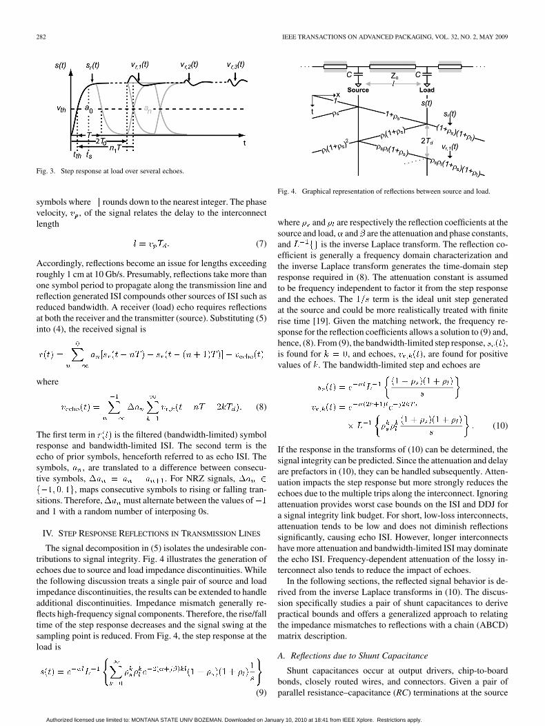
where is the interconnect delay. Fig. 3 illustrates the stepresponse described in (5). Initially, the step arrives at the loadand takes seconds to arrive at the nominal threshold voltage,
; by definition . The optimal sampling time,, is assumed to occur seconds after . Then, the th
echo arrives back at the load after seconds. During thisinterval, symbols are subsequently transmitted. The th re-flection arrives
(6)
Authorized licensed use limited to: MONTANA STATE UNIV BOZEMAN. Downloaded on January 10, 2010 at 18:41 from IEEE Xplore. Restrictions apply.
282 IEEE TRANSACTIONS ON ADVANCED PACKAGING, VOL. 32, NO. 2, MAY 2009
Fig. 3. Step response at load over several echoes.
symbols where rounds down to the nearest integer. The phasevelocity, , of the signal relates the delay to the interconnectlength
(7)
Accordingly, reflections become an issue for lengths exceedingroughly 1 cm at 10 Gb/s. Presumably, reflections take more thanone symbol period to propagate along the transmission line andreflection generated ISI compounds other sources of ISI such asreduced bandwidth. A receiver (load) echo requires reflectionsat both the receiver and the transmitter (source). Substituting (5)into (4), the received signal is
where
(8)
The first term in is the filtered (bandwidth-limited) symbolresponse and bandwidth-limited ISI. The second term is theecho of prior symbols, henceforth referred to as echo ISI. Thesymbols, , are translated to a difference between consecu-tive symbols, . For NRZ signals,
, maps consecutive symbols to rising or falling tran-sitions. Therefore, must alternate between the values ofand 1 with a random number of interposing 0s.
IV. STEP RESPONSE REFLECTIONS IN TRANSMISSION LINES
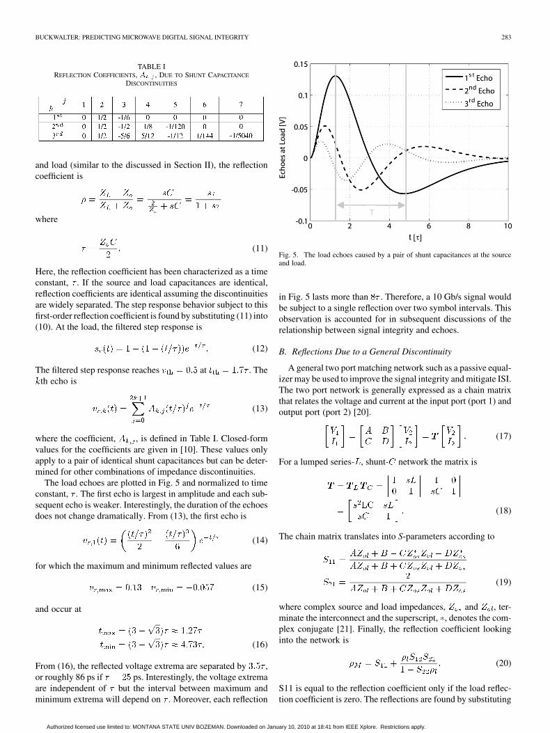
The signal decomposition in (5) isolates the undesirable con-tributions to signal integrity. Fig. 4 illustrates the generation ofechoes due to source and load impedance discontinuities. Whilethe following discussion treats a single pair of source and loadimpedance discontinuities, the results can be extended to handleadditional discontinuities. Impedance mismatch generally re-flects high-frequency signal components. Therefore, the rise/falltime of the step response decreases and the signal swing at thesampling point is reduced. From Fig. 4, the step response at theload is
(9)
Fig. 4. Graphical representation of reflections between source and load.
where and are respectively the reflection coefficients at thesource and load, and are the attenuation and phase constants,and is the inverse Laplace transform. The reflection co-efficient is generally a frequency domain characterization andthe inverse Laplace transform generates the time-domain stepresponse required in (8). The attenuation constant is assumedto be frequency independent to factor it from the step responseand the echoes. The term is the ideal unit step generatedat the source and could be more realistically treated with finiterise time [19]. Given the matching network, the frequency re-sponse for the reflection coefficients allows a solution to (9) and,hence, (8). From (9), the bandwidth-limited step response, ,is found for , and echoes, , are found for positivevalues of . The bandwidth-limited step and echoes are
(10)
If the response in the transforms of (10) can be determined, thesignal integrity can be predicted. Since the attenuation and delayare prefactors in (10), they can be handled subsequently. Atten-uation impacts the step response but more strongly reduces theechoes due to the multiple trips along the interconnect. Ignoringattenuation provides worst case bounds on the ISI and DDJ fora signal integrity link budget. For short, low-loss interconnects,attenuation tends to be low and does not diminish reflectionssignificantly, causing echo ISI. However, longer interconnectshave more attenuation and bandwidth-limited ISI may dominatethe echo ISI. Frequency-dependent attenuation of the lossy in-terconnect also tends to reduce the impact of echoes.
In the following sections, the reflected signal behavior is de-rived from the inverse Laplace transforms in (10). The discus-sion specifically studies a pair of shunt capacitances to derivepractical bounds and offers a generalized approach to relatingthe impedance mismatches to reflections with a chain (ABCD)matrix description.
A. Reflections due to Shunt Capacitance
Shunt capacitances occur at output drivers, chip-to-boardbonds, closely routed wires, and connectors. Given a pair ofparallel resistance–capacitance (RC) terminations at the source
Authorized licensed use limited to: MONTANA STATE UNIV BOZEMAN. Downloaded on January 10, 2010 at 18:41 from IEEE Xplore. Restrictions apply.
BUCKWALTER: PREDICTING MICROWAVE DIGITAL SIGNAL INTEGRITY 283
TABLE IREFLECTION COEFFICIENTS, � , DUE TO SHUNT CAPACITANCE
DISCONTINUITIES
and load (similar to the discussed in Section II), the reflectioncoefficient is
where
(11)
Here, the reflection coefficient has been characterized as a timeconstant, . If the source and load capacitances are identical,reflection coefficients are identical assuming the discontinuitiesare widely separated. The step response behavior subject to thisfirst-order reflection coefficient is found by substituting (11) into(10). At the load, the filtered step response is
(12)
The filtered step response reaches at . Theth echo is
(13)
where the coefficient, , is defined in Table I. Closed-formvalues for the coefficients are given in [10]. These values onlyapply to a pair of identical shunt capacitances but can be deter-mined for other combinations of impedance discontinuities.
The load echoes are plotted in Fig. 5 and normalized to timeconstant, . The first echo is largest in amplitude and each sub-sequent echo is weaker. Interestingly, the duration of the echoesdoes not change dramatically. From (13), the first echo is
(14)
for which the maximum and minimum reflected values are
(15)
and occur at
(16)
From (16), the reflected voltage extrema are separated by ,or roughly 86 ps if ps. Interestingly, the voltage extremaare independent of but the interval between maximum andminimum extrema will depend on . Moreover, each reflection
Fig. 5. The load echoes caused by a pair of shunt capacitances at the sourceand load.
in Fig. 5 lasts more than . Therefore, a 10 Gb/s signal wouldbe subject to a single reflection over two symbol intervals. Thisobservation is accounted for in subsequent discussions of therelationship between signal integrity and echoes.
B. Reflections Due to a General Discontinuity
A general two port matching network such as a passive equal-izer may be used to improve the signal integrity and mitigate ISI.The two port network is generally expressed as a chain matrixthat relates the voltage and current at the input port (port 1) andoutput port (port 2) [20].
(17)
For a lumped series- , shunt- network the matrix is
(18)
The chain matrix translates into S-parameters according to
(19)
where complex source and load impedances, and , ter-minate the interconnect and the superscript, , denotes the com-plex conjugate [21]. Finally, the reflection coefficient lookinginto the network is
(20)
S11 is equal to the reflection coefficient only if the load reflec-tion coefficient is zero. The reflections are found by substituting
Authorized licensed use limited to: MONTANA STATE UNIV BOZEMAN. Downloaded on January 10, 2010 at 18:41 from IEEE Xplore. Restrictions apply.
284 IEEE TRANSACTIONS ON ADVANCED PACKAGING, VOL. 32, NO. 2, MAY 2009
(20) into (10). Therefore, the echo that results from any arbitrarysource and load matching network is determined.
V. DIGITAL SIGNAL INTEGRITY
Characterizing the eye closure in the voltage and time do-mains is possible given the filtered step and echo response. Inthe first part of this section, the step response is related to band-width-limited ISI and DDJ. In the second part of this section,the reflections are related to the echo ISI and DDJ. Eye closurefor an interconnect limited by source and load shunt capacitanceprovides an example to find bounds on the ISI and DDJ.
A. Bandwidth-Limited ISI
The step response, , has a reduced rise and fall transitiontime that spreads signal energy over neighboring symbols. Thebandwidth-limited peak ISI is
where
(21)
The bandwidth-limited ISI is the residual deviation of the stepresponse from the voltage swing at symbol intervals from thesampling time of the current symbol. The eye height is the dif-ference between the minimum voltage associated with the log-ical value of one and the maximum voltage associated with thelogical value of zero at the sampling point
(22)
The first term in (22) accounts for the step response at the de-sired symbol while the second term is the peak ISI caused bythe residual deviation at the sampling point. The sampling pointoccurs roughly seconds after the threshold crossing time inmost instances, i.e., .
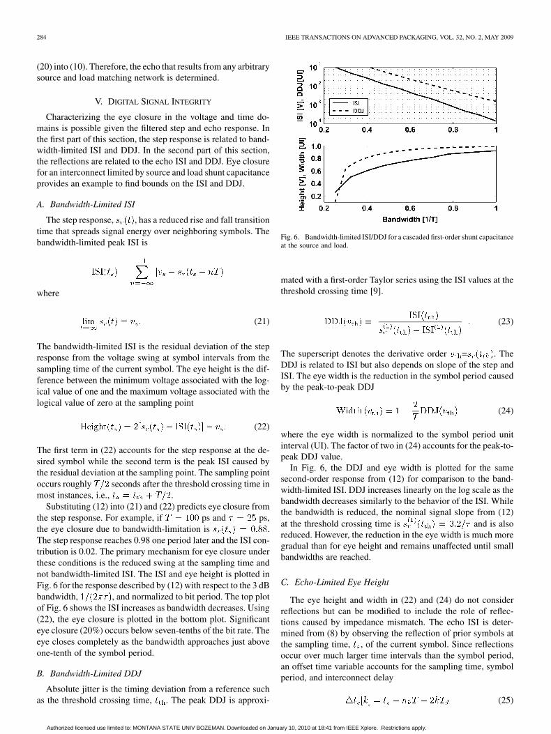
Substituting (12) into (21) and (22) predicts eye closure fromthe step response. For example, if ps and ps,the eye closure due to bandwidth-limitation is .The step response reaches 0.98 one period later and the ISI con-tribution is 0.02. The primary mechanism for eye closure underthese conditions is the reduced swing at the sampling time andnot bandwidth-limited ISI. The ISI and eye height is plotted inFig. 6 for the response described by (12) with respect to the 3 dBbandwidth, , and normalized to bit period. The top plotof Fig. 6 shows the ISI increases as bandwidth decreases. Using(22), the eye closure is plotted in the bottom plot. Significanteye closure (20%) occurs below seven-tenths of the bit rate. Theeye closes completely as the bandwidth approaches just aboveone-tenth of the symbol period.
B. Bandwidth-Limited DDJ
Absolute jitter is the timing deviation from a reference suchas the threshold crossing time, . The peak DDJ is approxi-
Fig. 6. Bandwidth-limited ISI/DDJ for a cascaded first-order shunt capacitanceat the source and load.
mated with a first-order Taylor series using the ISI values at thethreshold crossing time [9].
(23)
The superscript denotes the derivative order = . TheDDJ is related to ISI but also depends on slope of the step andISI. The eye width is the reduction in the symbol period causedby the peak-to-peak DDJ
(24)
where the eye width is normalized to the symbol period unitinterval (UI). The factor of two in (24) accounts for the peak-to-peak DDJ value.
In Fig. 6, the DDJ and eye width is plotted for the samesecond-order response from (12) for comparison to the band-width-limited ISI. DDJ increases linearly on the log scale as thebandwidth decreases similarly to the behavior of the ISI. Whilethe bandwidth is reduced, the nominal signal slope from (12)at the threshold crossing time is and is alsoreduced. However, the reduction in the eye width is much moregradual than for eye height and remains unaffected until smallbandwidths are reached.
C. Echo-Limited Eye Height
The eye height and width in (22) and (24) do not considerreflections but can be modified to include the role of reflec-tions caused by impedance mismatch. The echo ISI is deter-mined from (8) by observing the reflection of prior symbols atthe sampling time, , of the current symbol. Since reflectionsoccur over much larger time intervals than the symbol period,an offset time variable accounts for the sampling time, symbolperiod, and interconnect delay
(25)
Authorized licensed use limited to: MONTANA STATE UNIV BOZEMAN. Downloaded on January 10, 2010 at 18:41 from IEEE Xplore. Restrictions apply.
BUCKWALTER: PREDICTING MICROWAVE DIGITAL SIGNAL INTEGRITY 285
where is defined in (6). From this offset time, the ISI from(8) becomes
(26)
The maximum value is taken over all possible combinations fordata transition values, . To further simplify this expression,the total echo ISI can be decomposed into an individual ISI con-tributions from the th echo
(27)
and . Since reflections decay with time,the summation includes few symbols after . To illustrate thispoint, a symbol period of is superimposed on the firstecho at the load in Fig. 5. The reflection lasts over two symbolperiod and takes values of 1 and 0 or 1 and since the
sequence must alternate. Subsequent positive and negativevalues of the reflection accentuate the echo ISI and the differ-ence between the symbol period delayed samples of the reflec-tion contributes to the th echo ISI. Therefore, the th echo ISIis simplified from (27) to
(28)
If reflections last over more than two symbols, (28) must includemore combinations of symbols. On the other hand, if the reflec-tion lasts over one symbol, the ISI depends only on the first termin (28).
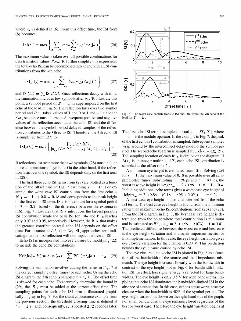
The first three echo ISI terms from (28) are plotted as a func-tion of the offset time in Fig. 7 assuming . For ex-ample, the worst case ISI contribution from the first echo is
and corresponds to the peak heightof the first echo ISI term. is maximum for a symbol periodof based on the difference between the extrema in(16). Fig. 7 illustrates that introduces the largest possibleISI contribution while the peak ISI for and reachesonly 0.07 and 0.05, respectively. However, the that makesthe greatest contribution total echo ISI depends on the offsettime. For instance, at , approaches zero indi-cating that the first reflection will not impact the overall ISI.
Echo ISI is incorporated into eye closure by modifying (22)to include the echo ISI contributions
(29)
Solving the summation involves adding the terms in Fig. 7 atthe correct sampling offset times for each echo. Using the echoISI diagram, the th echo is sampled at . The offset timeis skewed for each echo. To accurately determine the bound in(29), the must be added at the correct offset time. Thesampling points for each echo ISI term is illustrated graphi-cally in gray in Fig. 7. For the shunt capacitance example fromthe previous section, the threshold crossing time is defined at
and, consequently, is located seconds later.
Fig. 7. The worst case contributions to ISI and DDJ from the �th echo at theload for � � �� .
The first echo ISI term is sampled at , whereis the modulo operator. In the example in Fig. 7, the peak
of the first echo ISI contribution is sampled. Subsequent sampleswrap around by the interconnect delay modulo the symbol pe-riod. The second echo ISI term is sampled at .The sampling location of each is circled on the diagram. If
is an integer multiple of , each echo ISI contribution issampled at the offset time .
A minimum eye height is estimated from . Solving (29)for , the maximum value of 0.18 is possible over all sam-pling offset times. Substituting ps and ps, theworst case eye height is .Including additional echo terms gives a worst case eye height of
.A best case eye height is also characterized from the echo
ISI terms. The best case eye height is found from the minimumrather than maximum echo ISI contributions from (26) and (27).From the ISI diagram in Fig. 7, the best case eye height is de-termined from the point where total contribution is minimumand is estimated as .The predicted difference between the worst-case and best-caseis the eye height variation and is also an important metric forlink implementation. In this case, the eye height variation giveseye closure variation for the channel is 0.37 V. This predictionbounds the eye closure caused by echo ISI.
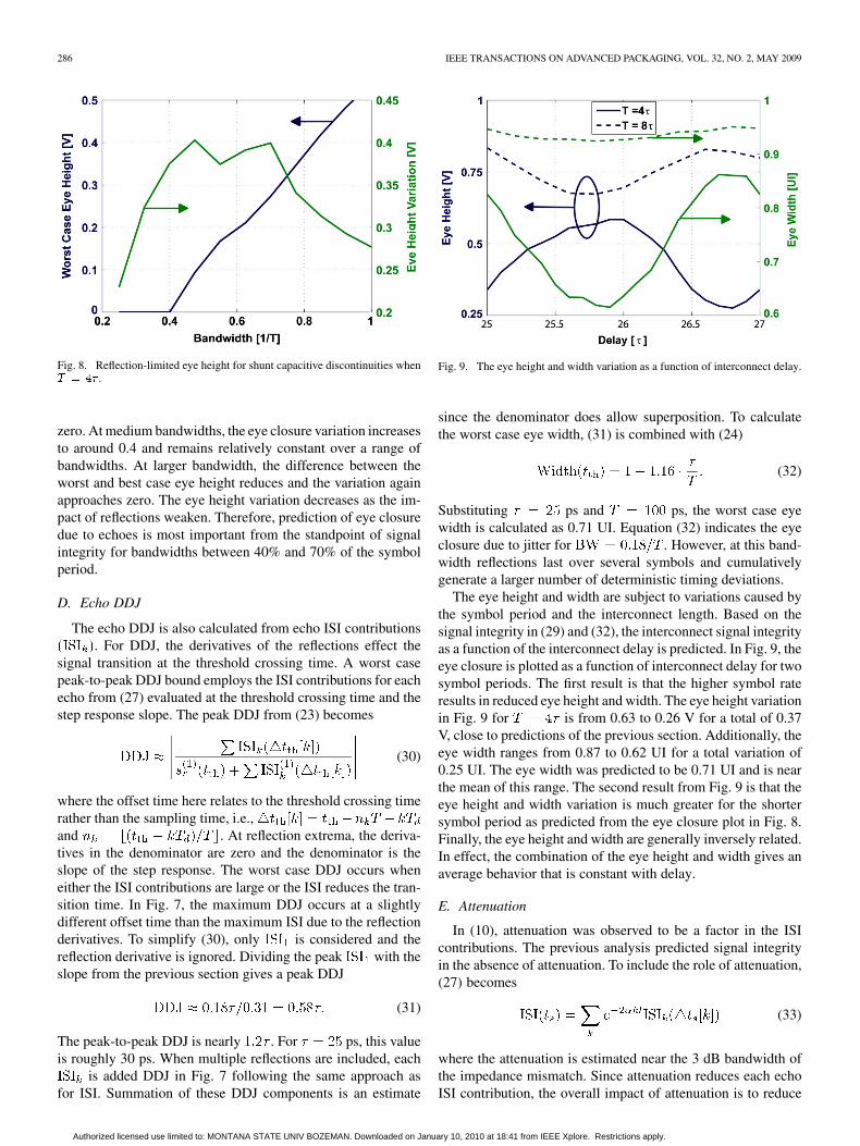
The eye closure due to echo ISI is plotted in Fig. 8 as a func-tion of the bandwidth of the source and load impedance mis-match. The eye height increases linearly with the bandwidth incontrast to the eye height plot in Fig. 6 for bandwidth-limita-tion ISI. In effect, less signal energy is reflected for large band-widths. The eye height is only 0.5 V for wide bandwidths, im-plying that echo ISI dominates the bandwidth-limited ISI in theabsence of attenuation. In this case, echoes cause worst-case eyeclosure when the bandwidth is 40% of the symbol period. Theeye height variation is shown on the right-hand side of the graph.For small bandwidths, the eye remains closed regardless of thebest or worst case. Therefore the eye height variation begins at
Authorized licensed use limited to: MONTANA STATE UNIV BOZEMAN. Downloaded on January 10, 2010 at 18:41 from IEEE Xplore. Restrictions apply.
286 IEEE TRANSACTIONS ON ADVANCED PACKAGING, VOL. 32, NO. 2, MAY 2009
Fig. 8. Reflection-limited eye height for shunt capacitive discontinuities when� � �� .
zero. At medium bandwidths, the eye closure variation increasesto around 0.4 and remains relatively constant over a range ofbandwidths. At larger bandwidth, the difference between theworst and best case eye height reduces and the variation againapproaches zero. The eye height variation decreases as the im-pact of reflections weaken. Therefore, prediction of eye closuredue to echoes is most important from the standpoint of signalintegrity for bandwidths between 40% and 70% of the symbolperiod.
D. Echo DDJ
The echo DDJ is also calculated from echo ISI contributions. For DDJ, the derivatives of the reflections effect the
signal transition at the threshold crossing time. A worst casepeak-to-peak DDJ bound employs the ISI contributions for eachecho from (27) evaluated at the threshold crossing time and thestep response slope. The peak DDJ from (23) becomes
(30)
where the offset time here relates to the threshold crossing timerather than the sampling time, i.e.,and . At reflection extrema, the deriva-tives in the denominator are zero and the denominator is theslope of the step response. The worst case DDJ occurs wheneither the ISI contributions are large or the ISI reduces the tran-sition time. In Fig. 7, the maximum DDJ occurs at a slightlydifferent offset time than the maximum ISI due to the reflectionderivatives. To simplify (30), only is considered and thereflection derivative is ignored. Dividing the peak with theslope from the previous section gives a peak DDJ
(31)
The peak-to-peak DDJ is nearly . For ps, this valueis roughly 30 ps. When multiple reflections are included, each
is added DDJ in Fig. 7 following the same approach asfor ISI. Summation of these DDJ components is an estimate
Fig. 9. The eye height and width variation as a function of interconnect delay.
since the denominator does allow superposition. To calculatethe worst case eye width, (31) is combined with (24)
(32)
Substituting ps and ps, the worst case eyewidth is calculated as 0.71 UI. Equation (32) indicates the eyeclosure due to jitter for . However, at this band-width reflections last over several symbols and cumulativelygenerate a larger number of deterministic timing deviations.
The eye height and width are subject to variations caused bythe symbol period and the interconnect length. Based on thesignal integrity in (29) and (32), the interconnect signal integrityas a function of the interconnect delay is predicted. In Fig. 9, theeye closure is plotted as a function of interconnect delay for twosymbol periods. The first result is that the higher symbol rateresults in reduced eye height and width. The eye height variationin Fig. 9 for is from 0.63 to 0.26 V for a total of 0.37V, close to predictions of the previous section. Additionally, theeye width ranges from 0.87 to 0.62 UI for a total variation of0.25 UI. The eye width was predicted to be 0.71 UI and is nearthe mean of this range. The second result from Fig. 9 is that theeye height and width variation is much greater for the shortersymbol period as predicted from the eye closure plot in Fig. 8.Finally, the eye height and width are generally inversely related.In effect, the combination of the eye height and width gives anaverage behavior that is constant with delay.
E. Attenuation
In (10), attenuation was observed to be a factor in the ISIcontributions. The previous analysis predicted signal integrityin the absence of attenuation. To include the role of attenuation,(27) becomes
(33)
where the attenuation is estimated near the 3 dB bandwidth ofthe impedance mismatch. Since attenuation reduces each echoISI contribution, the overall impact of attenuation is to reduce
Authorized licensed use limited to: MONTANA STATE UNIV BOZEMAN. Downloaded on January 10, 2010 at 18:41 from IEEE Xplore. Restrictions apply.
BUCKWALTER: PREDICTING MICROWAVE DIGITAL SIGNAL INTEGRITY 287
Fig. 10. Simulated eye height and width variation as a function of interconnectlength.
echo ISI. Since reflections have high-frequency energy content,they are more susceptible to frequency-dependent attenuation.
F. Comparison With Full Time Domain Simulations
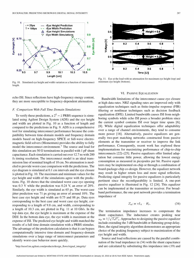
To verify these predictions, a PRBS sequence is simu-lated using Agilent Design System (ADS) and the eye heightand width are plotted in Fig. 10 as a function of length andcompared to the predictions in Fig. 9. ADS is a comprehensivetool for simulating interconnect performance because the com-patibility between time-domain models and frequency domainmodels based on high-frequency SPICE or full-wave electro-magnetic field solvers (Momentum) provides the ability to fullymodel the interconnect environment. The source and load forthis simulation are 50 terminations in parallel with 1 pF shuntcapacitance. Each simulation is carried out over 12.7 ns with 200fs timing resolution. The interconnect model is an ideal trans-mission line of nominal length of 10 cm. No attenuation is mod-eled to provide worst-case comparison with the predictions. Theeye diagram is simulated at 0.1 cm intervals and the eye closureis plotted in Fig. 10. The maximum and minimum values for theeye height and width of the simulations agree with the predic-tions. Fig. 10 shows that the simulated worst case eye openingwas 0.3 V while the prediction was 0.24 V, an error of 20%.Similarly, the eye width is simulated as 65 ps. The worst-casejitter prediction was 71 ps giving an error of around 10%. Thebest case eye height and width are 0.75 and 88 ps. Data eyescorresponding to the best case and worst case eye height, cor-responding to a length of 9.8 cm, and width, corresponding toa length of 10.3 cm, are plotted in Fig. 11 at 10 Gb/s. In thetop data eye, the eye height is maximum at the expense of theDDJ. In the bottom data eye, the eye width is maximum at theexpense of ISI. The predicted eye height and width matched theresults of a full time domain simulation with a PRBS stimulus.The advantage of the prediction calculation is that it can bypasscomputationally intensive time-domain and frequency-domainsimulations over a large range of interconnect parameters andidentify worst-case behavior more quickly.
1http://eesof.tm.agilent.com/products/design_flows/signal_integrity/
Fig. 11. Eye at the load with no attenuation for maximum eye height (top) andminimum eye height (bottom).
VI. PASSIVE EQUALIZATION
Bandwidth limitations of the interconnect cause eye closureat high data rates. NRZ signaling rates are improved only withequalization techniques such as finite-impulse response (FIR)filtering or nonlinear techniques such as decision feedbackequalization (DFE). Limited bandwidth causes ISI from neigh-boring symbols while echo ISI poses a broader problem sincethe current symbol contains ISI over larger time spans [6],[8]. While digital equalization techniques offer adaptabilityover a range of channel environments, they tend to consumemore power [18]. Alternatively, passive equalizers are gen-erally two-port matching networks constructed from passiveelements at the transmitter or receiver to improve the linkperformance. Consequently, recent work has explored theseimplementations for maximizing performance of chip-to-chipinterconnects [22]–[25]. Passive equalizers offer limited adap-tation but consume little power, allowing the lowest energyconsumption as measured in picojoules per bit. Passive equal-izers may be implemented on-chip or through a combination ofboard-package-chip co-design. However, the equalizer networkmay result in higher return loss and more signal reflection.Predicting signal integrity for passive equalizers is particularlypertinent since the reconfigurability is limited. A one-portpassive equalizer is illustrated in Fig. 12 [24]. This equalizercan be implemented at the transmitter or receiver. For broad-band performance, the one-port network provides a terminationimpedance of
(34)
The termination impedance increases to compensate theshunt capacitance. The inductance creates peaking near
. Approaches to designing the passive equalizerinclude extending the 3 dB bandwidth or flattening group delay.Here, the signal integrity algorithm demonstrates an appropriatechoice of the peaking frequency subject to maximization of theeye height and width.
Source and load reflections are caused by the parallel combi-nation of the load impedance in (34) with the shunt capacitanceand are calculated by substituting this impedance into (19) and
Authorized licensed use limited to: MONTANA STATE UNIV BOZEMAN. Downloaded on January 10, 2010 at 18:41 from IEEE Xplore. Restrictions apply.
288 IEEE TRANSACTIONS ON ADVANCED PACKAGING, VOL. 32, NO. 2, MAY 2009
Fig. 12. One-port passive equalization.
Fig. 13. Predicted eye height and width as a function of series peakingfrequency.
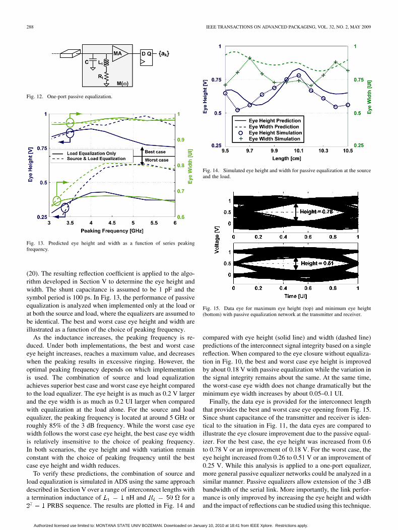
(20). The resulting reflection coefficient is applied to the algo-rithm developed in Section V to determine the eye height andwidth. The shunt capacitance is assumed to be 1 pF and thesymbol period is 100 ps. In Fig. 13, the performance of passiveequalization is analyzed when implemented only at the load orat both the source and load, where the equalizers are assumed tobe identical. The best and worst case eye height and width areillustrated as a function of the choice of peaking frequency.
As the inductance increases, the peaking frequency is re-duced. Under both implementations, the best and worst caseeye height increases, reaches a maximum value, and decreaseswhen the peaking results in excessive ringing. However, theoptimal peaking frequency depends on which implementationis used. The combination of source and load equalizationachieves superior best case and worst case eye height comparedto the load equalizer. The eye height is as much as 0.2 V largerand the eye width is as much as 0.2 UI larger when comparedwith equalization at the load alone. For the source and loadequalizer, the peaking frequency is located at around 5 GHz orroughly 85% of the 3 dB frequency. While the worst case eyewidth follows the worst case eye height, the best case eye widthis relatively insensitive to the choice of peaking frequency.In both scenarios, the eye height and width variation remainconstant with the choice of peaking frequency until the bestcase eye height and width reduces.
To verify these predictions, the combination of source andload equalization is simulated in ADS using the same approachdescribed in Section V over a range of interconnect lengths witha termination inductance of nH and for a
PRBS sequence. The results are plotted in Fig. 14 and
Fig. 14. Simulated eye height and width for passive equalization at the sourceand the load.
Fig. 15. Data eye for maximum eye height (top) and minimum eye height(bottom) with passive equalization network at the transmitter and receiver.
compared with eye height (solid line) and width (dashed line)predictions of the interconnect signal integrity based on a singlereflection. When compared to the eye closure without equaliza-tion in Fig. 10, the best and worst case eye height is improvedby about 0.18 V with passive equalization while the variation inthe signal integrity remains about the same. At the same time,the worst-case eye width does not change dramatically but theminimum eye width increases by about 0.05–0.1 UI.
Finally, the data eye is provided for the interconnect lengththat provides the best and worst case eye opening from Fig. 15.Since shunt capacitance of the transmitter and receiver is iden-tical to the situation in Fig. 11, the data eyes are compared toillustrate the eye closure improvement due to the passive equal-izer. For the best case, the eye height was increased from 0.6to 0.78 V or an improvement of 0.18 V. For the worst case, theeye height increased from 0.26 to 0.51 V or an improvement of0.25 V. While this analysis is applied to a one-port equalizer,more general passive equalizer networks could be analyzed in asimilar manner. Passive equalizers allow extension of the 3 dBbandwidth of the serial link. More importantly, the link perfor-mance is only improved by increasing the eye height and widthand the impact of reflections can be studied using this technique.
Authorized licensed use limited to: MONTANA STATE UNIV BOZEMAN. Downloaded on January 10, 2010 at 18:41 from IEEE Xplore. Restrictions apply.
BUCKWALTER: PREDICTING MICROWAVE DIGITAL SIGNAL INTEGRITY 289
VII. CONCLUSION
A method for predicting signal integrity identifies the rela-tionship between signal echoes and the interconnect impedancemismatch, symbol period, and interconnect delay. The advan-tage of this method is that interconnect eye height and width areassessed quickly without extensive time domain simulation overall parameters. This paper examines the fundamental trade-offbetween bandwidth and return loss. For linear channels, the im-pact of impedance mismatch is separated into components af-fecting the step response (bandwidth-limited ISI) and gener-ating echoes (reflection-limited ISI). The relationship betweenechoes and signal integrity in serial links is derived and an anal-ysis for predicting best and worst case signal integrity is de-scribed. Bounds on the intersymbol interference and data-de-pendent jitter are constructed for capacitive discontinuities andcompared to simulation results. Finally, this predictive signalintegrity technique is applied to the design of a passive equal-izer to show the optimal choice of peaking inductance for eyeclosure.
REFERENCES
[1] H. Johnson and M. Graham, High-Speed Signal Propagation. UpperSaddle River, NJ: Prentice Hall.
[2] International Technology Roadmap for Semiconductors—Intercon-nects 2007.
[3] P. Mehrotra et al., “Optimal chip-package codesign for high-perfor-mance DSP,” IEEE Trans. Adv. Packag., vol. 28, no. 2, pp. 288–297,May 2005.
[4] W. Beyene et al., “Design, modeling, and hardware correlation of a 3.2Gb/s/pair memory channel,” IEEE Trans. Adv. Packag., vol. 27, no. 1,pp. 34–44, Feb. 2004.
[5] H. Braunisch et al., “High-speed flex-circuit chip-to-chip intercon-nects,” IEEE Trans. Adv. Packag., vol. 31, no. 1, pp. 82–90, Feb. 2008.
[6] J. F. Buckwalter, B. Analui, and A. Hajimiri, “Data-dependent jitter andcrosstalk-induced bounded uncorrelated jitter in copper interconnects,”in IEEE Int. Microw. Symp. Dig., Jun. 6-11, 2004, pp. 1627–1630.
[7] L. Zhang, W. Yu, Y. Zhang, R. Wang, A. Deutsch, G. A. Katopis, D. M.Dreps, J. Buckwalter, E. S. Kuh, and C. K. Cheng, “Low power passiveequalizer design for computer memory links,” in IEEE Hot Intercon-nects Symp. High Performance Interconnects, Aug. 2008, pp. 51–56.
[8] B. Analui, J. F. Buckwalter, and A. Hajimiri, “Data-dependent jitter inserial communications,” IEEE Trans. Microwave Theory Techniques,vol. 53, pp. 3388–3397, Nov. 2005.
[9] J. F. Buckwalter, B. Analui, and A. Hajimiri, “Predicting data-depen-dent jitter,” IEEE Trans. Circuits Syst. II, vol. 51, no. 9, pp. 453–457,Sep. 2004.
[10] J. F. Buckwalter, “Signal integrity in reflection-limited channels,” inIEEE Int. Microwave Symp. Dig., Jun. 16-19, 2008, pp. 1565–1568.
[11] Fibre channel—Methodologies for jitter and signal quality specifica-tion-MJSQ International Committee for Information Technology Stan-dardization (INCITS),, Tech. Rep. REV 12, Nov. 2005.
[12] IEEE P802.3ae XAUI Interface Standard, , 2006.[13] C.-J. Ong, B. Wu, L. Tsang, and X. Gu, “Full-wave solver for mi-
crostrip trace and through-hole via in layered media,” IEEE Trans. Adv.Packag., vol. 31, no. 5, pp. 292–302, May 2008.
[14] R. M. Fano, “Theoretical limitations on the broadband matching ofarbitrary functions,” J. Franklin Instit., vol. 249, pp. 57–83, Jan. 1950.
[15] H. Bode, Network Analysis and Feedback Amplifier Design. NewYork: Van Nostrand, 1945.
[16] B. Analui and A. Hajimiri, “Bandwidth enhancement of tran-simpedance amplifiers,” IEEE J. Solid-State Circuits, vol. 53, no. 11,pp. 1263–1270, Nov. 2005.
[17] T. P. Budka, “Wide-bandwidth millimeter-wave bond-wire inter-connects,” IEEE Trans. Microwave Theory Tech., vol. 49, no. 4, pp.715–718, Apr. 2001.
[18] J. Zerbe et al., “Equalization and clock recovery for a 2.5–10-Gb/s2-PAM/4-PAM backplane transceiver cell,” IEEE J. Solid-State Cir-cuits, vol. 38, no. 12, pp. 2121–2130, Dec. 2003.
[19] B. Young, Digital Signal Integrity. Upper Saddle River, NJ: PrenticeHall.
[20] D. M. Pozar, Microwave Engineering. New York: Wiley, 2005.[21] D. A. Frickey, “Conversions between S, Z, Y, H, ABCD, and T param-
eters which are valid for complex source and load impedances,” IEEETrans. Microwave Theory Tech., vol. 42, no. 2, pp. 205–211, Feb. 1994.
[22] K. J. Han, H. Takeuchi, and M. Swaminathan, “Eye-pattern designfor high-speed differential links using extended passive equalization,”IEEE Trans. Adv. Packag., vol. 31, no. 2, pp. 246–257, May 2008.
[23] R. Sun, J. Park, F. O’Mahoney, and C. P. Yue, “A tunable passive filterfor low-power high-speed equalizers,” in IEEE Symp. VLSI Circ., Jun.2006, p. 198.
[24] G. Balamuragan, “A scalable 5–15 Gbps, 14–75 mW low-power I/Otransceiver in 65 nm CMOS,” IEEE J. Solid-State Circuits, vol. 43, no.4, pp. 1010–1019, Apr. 2008.
[25] Y. Zhang, L. Zhang, A. Deutsch, G. A. Katopis, D. M. Dreps, J. F.Buckwalter, E. S. Kuh, and C. K. Cheng, “On-chip bus signalingusing passive compensation,” IEEE Electrical Performance ElectronicPackag., pp. 33–36, Oct. 2008.
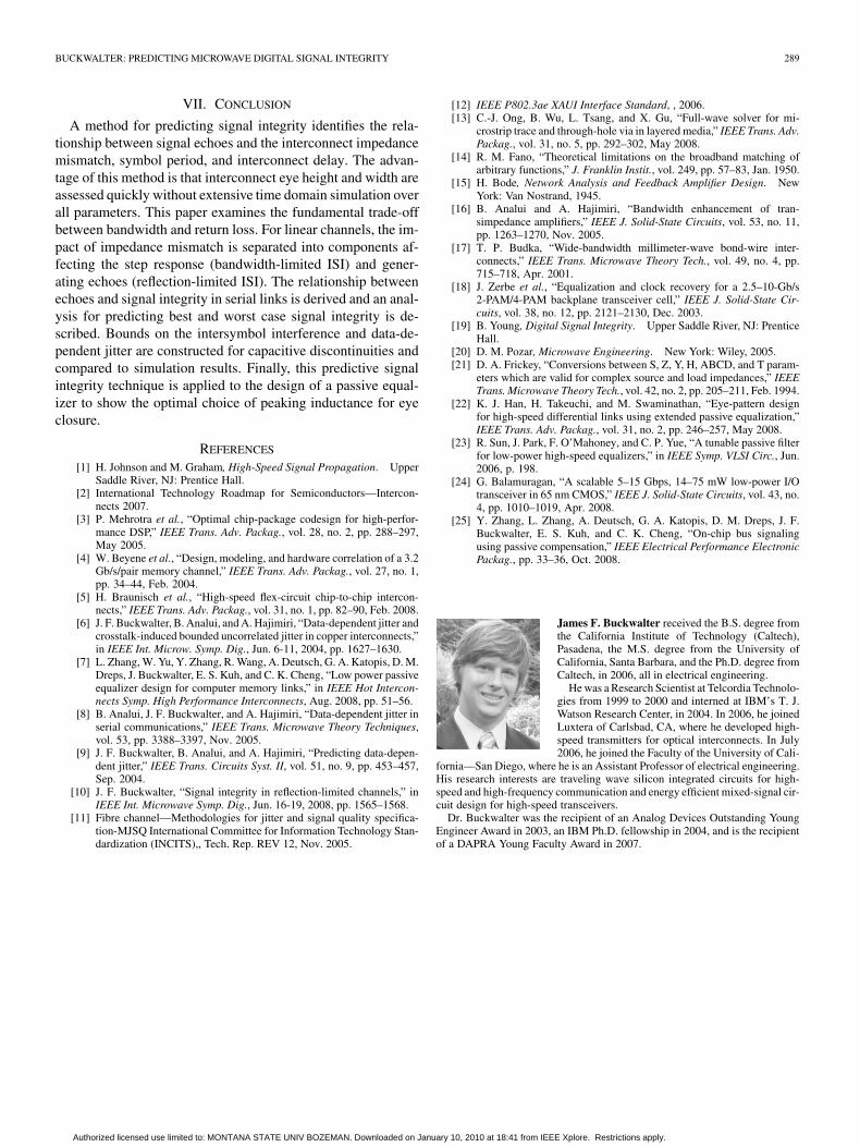
James F. Buckwalter received the B.S. degree fromthe California Institute of Technology (Caltech),Pasadena, the M.S. degree from the University ofCalifornia, Santa Barbara, and the Ph.D. degree fromCaltech, in 2006, all in electrical engineering.
He was a Research Scientist at Telcordia Technolo-gies from 1999 to 2000 and interned at IBM’s T. J.Watson Research Center, in 2004. In 2006, he joinedLuxtera of Carlsbad, CA, where he developed high-speed transmitters for optical interconnects. In July2006, he joined the Faculty of the University of Cali-
fornia—San Diego, where he is an Assistant Professor of electrical engineering.His research interests are traveling wave silicon integrated circuits for high-speed and high-frequency communication and energy efficient mixed-signal cir-cuit design for high-speed transceivers.
Dr. Buckwalter was the recipient of an Analog Devices Outstanding YoungEngineer Award in 2003, an IBM Ph.D. fellowship in 2004, and is the recipientof a DAPRA Young Faculty Award in 2007.
Authorized licensed use limited to: MONTANA STATE UNIV BOZEMAN. Downloaded on January 10, 2010 at 18:41 from IEEE Xplore. Restrictions apply.