Embed Size (px)
Citation preview

± 2g / 4g / 8g / 16g Tri-axis Digital Accelerometer Specifications
PART NUMBER:
KXTJ3-1057
Rev. 3.0
27-Sep-2017
36 Thornwood Dr. – Ithaca, NY 14850 © 2017 Kionix – All Rights Reserved
tel: 607-257-1080 – fax:607-257-1146 762-9990-1709291201
www.kionix.com - [email protected] Page 1 of 42
Product Description
The KXTJ3-1057 is a tri-axis ±2g, ±4g, ±8g, or ±16g silicon
micromachined accelerometer. The sense element is fabricated using
Kionix’s proprietary plasma micromachining process technology.
Acceleration sensing is based on the principle of a differential
capacitance arising from acceleration-induced motion of the sense
element, which further utilizes common mode cancellation to decrease
errors from process variation, temperature, and environmental stress.
The sense element is hermetically sealed at the wafer level by bonding
a second silicon lid wafer to the device using a glass frit. A separate
ASIC device packaged with the sense element provides signal
conditioning and digital communications. The accelerometer is
delivered in a 2 x 2 x 0.9 mm LGA plastic package operating from a 1.71V – 3.6V DC supply. Voltage
regulators are used to maintain constant internal operating voltages over the range of input supply voltages.
This results in stable operating characteristics over the range of input supply voltages and virtually
undetectable ratiometric error. The I2C digital protocol is used to communicate with the chip to configure
the part and monitor outputs.
Features
• Small footprint: 2 x 2 x 0.9 mm LGA 12-pin package (pin-to-pin compatible with KXTJ2)
• Low current consumption: 0.9 µA in standby, 10 µA in Low Power, and 155 µA in High Resolution modes
• Extended user-configurable g-ranges: ±2g, ±4g, ±8g, ±16g
• 8-bit, 12-bit, and 14-bit resolution modes
• Wide supply voltage range: 1.71V – 3.6V with internal voltage regulator
• High resolution Wake-Up function with threshold configurable down to 3.9 mg
• User-configurable Output Data Rates from 0.781Hz to 1600Hz
• I2C digital communication interface up to 3.4MHz
• Highly configurable interrupt control
• Embedded Low Pass filter
• Improved design to virtually eliminate post reflow offset and sensitivity shifts
• Improved noise performance
• Stable performance over temperature
• High shock survivability
• Self-test function
• RoHS / REACH compliant
± 2g / 4g / 8g / 16g Tri-axis Digital Accelerometer Specifications
PART NUMBER:
KXTJ3-1057
Rev. 3.0
27-Sep-2017
36 Thornwood Dr. – Ithaca, NY 14850 © 2017 Kionix – All Rights Reserved
tel: 607-257-1080 – fax:607-257-1146 762-9990-1709291201
www.kionix.com - [email protected] Page 2 of 42
Table of Contents
PRODUCT DESCRIPTION .............................................................................................................................................................. 1
FEATURES ................................................................................................................................................................................... 1
TABLE OF CONTENTS ................................................................................................................................................................... 2
FUNCTIONAL DIAGRAM .............................................................................................................................................................. 4
PRODUCT SPECIFICATIONS .......................................................................................................................................................... 5
MECHANICAL .................................................................................................................................................................................. 5 ELECTRICAL ..................................................................................................................................................................................... 6
Start Up Time Profile .................................................................................................................................................................. 7 Current Profile ............................................................................................................................................................................ 8 Power-On Procedure .................................................................................................................................................................. 9
ENVIRONMENTAL ......................................................................................................................................................................... 10 Soldering ................................................................................................................................................................................... 11 Floor Life ................................................................................................................................................................................... 11
TERMINOLOGY .............................................................................................................................................................................. 12 g ................................................................................................................................................................................................ 12 Sensitivity ................................................................................................................................................................................. 12 Zero-g offset ............................................................................................................................................................................. 12 Self-test..................................................................................................................................................................................... 12
FUNCTIONALITY ............................................................................................................................................................................ 13 Sense element .......................................................................................................................................................................... 13 ASIC interface ........................................................................................................................................................................... 13 Factory calibration ................................................................................................................................................................... 13
APPLICATION SCHEMATIC ............................................................................................................................................................. 14 PIN DESCRIPTION .......................................................................................................................................................................... 14 PACKAGE DIMENSIONS AND ORIENTATION ................................................................................................................................. 15
Dimensions ............................................................................................................................................................................... 15 Orientation ............................................................................................................................................................................... 16
DIGITAL INTERFACE ................................................................................................................................................................... 20
I2C SERIAL INTERFACE ................................................................................................................................................................... 20 I2C OPERATION .............................................................................................................................................................................. 20 WRITING TO AN 8-BIT REGISTER ................................................................................................................................................... 22 READING FROM AN 8-BIT REGISTER ............................................................................................................................................. 22 DATA TRANSFER SEQUENCES ....................................................................................................................................................... 23 HS-MODE ...................................................................................................................................................................................... 24 I2C TIMING DIAGRAM.................................................................................................................................................................... 25
EMBEDDED REGISTERS.............................................................................................................................................................. 26
± 2g / 4g / 8g / 16g Tri-axis Digital Accelerometer Specifications
PART NUMBER:
KXTJ3-1057
Rev. 3.0
27-Sep-2017
36 Thornwood Dr. – Ithaca, NY 14850 © 2017 Kionix – All Rights Reserved
tel: 607-257-1080 – fax:607-257-1146 762-9990-1709291201
www.kionix.com - [email protected] Page 3 of 42
REGISTER DESCRIPTIONS........................................................................................................................................................... 27
ACCELEROMETER OUTPUTS .......................................................................................................................................................... 27 XOUT_L ......................................................................................................................................................................................... 29 XOUT_H ......................................................................................................................................................................................... 29 YOUT_L .......................................................................................................................................................................................... 29 YOUT_H ......................................................................................................................................................................................... 29 ZOUT_L .......................................................................................................................................................................................... 30 ZOUT_H ......................................................................................................................................................................................... 30 DCST_RESP .................................................................................................................................................................................... 30 WHO_AM_I ................................................................................................................................................................................... 30 INTERRUPT SOURCE REGISTERS .................................................................................................................................................... 31 INT_SOURCE1 ................................................................................................................................................................................ 31 INT_SOURCE2 ................................................................................................................................................................................ 31 STATUS_REG ................................................................................................................................................................................. 32 INT_REL ......................................................................................................................................................................................... 32 CTRL_REG1 .................................................................................................................................................................................... 33 CTRL_REG2 .................................................................................................................................................................................... 34 INT_CTRL_REG1 ............................................................................................................................................................................ 35 INT_CTRL_REG2 ............................................................................................................................................................................ 36 DATA_CTRL_REG ........................................................................................................................................................................... 36 WAKEUP_COUNTER ...................................................................................................................................................................... 37 NA_COUNTER................................................................................................................................................................................ 38 SELF_TEST ..................................................................................................................................................................................... 38 WAKEUP_THRESHOLD .................................................................................................................................................................. 38
EMBEDDED WAKE UP FUNCTION .............................................................................................................................................. 39
REVISION HISTORY .................................................................................................................................................................... 41
APPENDIX ................................................................................................................................................................................. 42
± 2g / 4g / 8g / 16g Tri-axis Digital Accelerometer Specifications
PART NUMBER:
KXTJ3-1057
Rev. 3.0
27-Sep-2017
36 Thornwood Dr. – Ithaca, NY 14850 © 2017 Kionix – All Rights Reserved
tel: 607-257-1080 – fax:607-257-1146 762-9990-1709291201
www.kionix.com - [email protected] Page 4 of 42
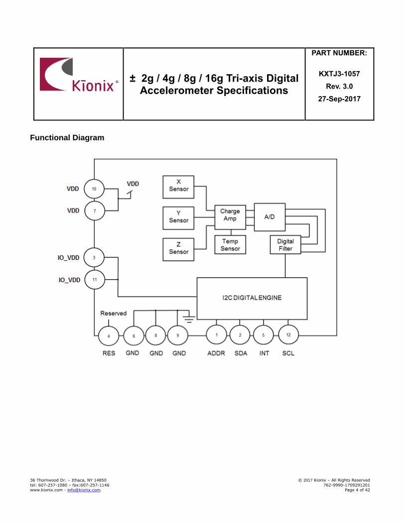
Functional Diagram
± 2g / 4g / 8g / 16g Tri-axis Digital Accelerometer Specifications
PART NUMBER:
KXTJ3-1057
Rev. 3.0
27-Sep-2017
36 Thornwood Dr. – Ithaca, NY 14850 © 2017 Kionix – All Rights Reserved
tel: 607-257-1080 – fax:607-257-1146 762-9990-1709291201
www.kionix.com - [email protected] Page 5 of 42
Product Specifications
Mechanical
(specifications are for operation at 2.5V and T = 25C unless stated otherwise)
Parameters Units Min Typical Max
Operating Temperature Range °C -40 - +85
Zero-g Offset mg ±25
Zero-g Offset Variation from RT over Temp. mg/ºC 0.2
Sensitivity (14-bit)1,2 ± 8g
counts/g 1024
± 16g 512
Sensitivity (12-bit)1
± 2g
counts/g
1024
± 4g 512
± 8g 256
± 16g 128
Sensitivity (8-bit)1
± 2g
counts/g
64
± 4g 32
± 8g 16
± 16g 8
Sensitivity Variation from RT over Temp. %/°C 0.01
Positive Self-test Output change on Activation3 g 0.5
Signal Bandwidth (-3dB) Hz
3500 (xy) 1800 (z)
Non-Linearity % of FS 0.6
Cross Axis Sensitivity % 2
Noise4 RMS Noise mg 0.7
Noise Density µg / √Hz 150
Table 1: Mechanical Specifications Notes:
1. Resolution and acceleration ranges are user selectable via I2C and via CTRL_REG1 register.
2. 14-bit Resolution is only available for registers 0x06 – 0x0B in the 8g or 16g High Resolution mode
3. Self-test can be exercised by setting STPOL bit = 1 in INT_CTRL_REG1, then writing 0xCA to the SELF_TEST register.
4. Noise measured in High Resolution Mode (RES = 1) at 50Hz ODR.

± 2g / 4g / 8g / 16g Tri-axis Digital Accelerometer Specifications
PART NUMBER:
KXTJ3-1057
Rev. 3.0
27-Sep-2017
36 Thornwood Dr. – Ithaca, NY 14850 © 2017 Kionix – All Rights Reserved
tel: 607-257-1080 – fax:607-257-1146 762-9990-1709291201
www.kionix.com - [email protected] Page 6 of 42
Electrical
(specifications are for operation at 2.5V and T = 25C unless stated otherwise)
Parameters Units Min Typical Max
Supply Voltage (VDD) Operating V 1.71 2.5 3.6
I/O Pads Supply Voltage (IO_VDD) V 1.7 3.6
Current Consumption
High Resolution Mode (RES=1)
µA
155
Low Power Mode1 (RES=0) 10
Disabled 0.9
Output Low Voltage (IO_VDD < 2V)2 V - - 0.2 * IO_VDD
Output Low Voltage (IO_VDD ≥ 2V)2 V - - 0.4
Output High Voltage V 0.8 * IO_VDD - -
Input Low Voltage V - - 0.2 * IO_VDD
Input High Voltage V 0.8 * IO_VDD - -
Start Up Time3 ms ~1/ODR
Power Up Time4 ms 12 30
I2C Communication Rate MHz 3.4
I2C Slave Address (7-bit) 0x0E / 0x0F
Output Data Rate (ODR)5 Hz 0.781 50 1600
Bandwidth (-3dB)6 RES = 0 800
RES = 1 ODR/2
Table 2: Electrical Specifications Notes:
1. Current varies with Output Data Rate (ODR). See Current Profile section for details. 2. For I2C communication, this assumes a minimum 1.5kΩ pull-up resistor on SCL and
SDA pins. 3. Start up time is from PC1 set to valid outputs. Time varies with Output Data Rate
(ODR). See Table 3: Start Up Time for details. 4. Power up time is from VDD and IO_VDD valid to device boot completion. 5. User selectable through I2C 6. User selectable and dependent on ODR and RES
± 2g / 4g / 8g / 16g Tri-axis Digital Accelerometer Specifications
PART NUMBER:
KXTJ3-1057
Rev. 3.0
27-Sep-2017
36 Thornwood Dr. – Ithaca, NY 14850 © 2017 Kionix – All Rights Reserved
tel: 607-257-1080 – fax:607-257-1146 762-9990-1709291201
www.kionix.com - [email protected] Page 7 of 42
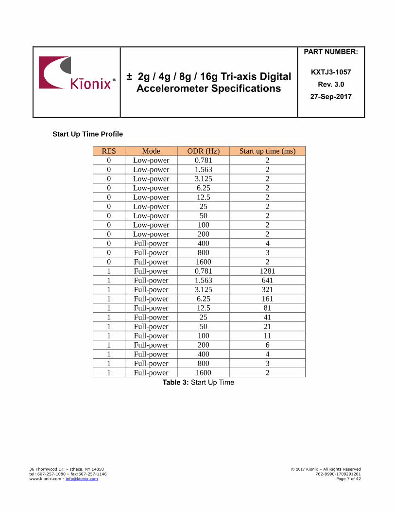
Start Up Time Profile
Table 3: Start Up Time
RES Mode ODR (Hz) Start up time (ms)
0 Low-power 0.781 2
0 Low-power 1.563 2
0 Low-power 3.125 2
0 Low-power 6.25 2
0 Low-power 12.5 2
0 Low-power 25 2
0 Low-power 50 2
0 Low-power 100 2
0 Low-power 200 2
0 Full-power 400 4
0 Full-power 800 3
0 Full-power 1600 2
1 Full-power 0.781 1281
1 Full-power 1.563 641
1 Full-power 3.125 321
1 Full-power 6.25 161
1 Full-power 12.5 81
1 Full-power 25 41
1 Full-power 50 21
1 Full-power 100 11
1 Full-power 200 6
1 Full-power 400 4
1 Full-power 800 3
1 Full-power 1600 2

± 2g / 4g / 8g / 16g Tri-axis Digital Accelerometer Specifications
PART NUMBER:
KXTJ3-1057
Rev. 3.0
27-Sep-2017
36 Thornwood Dr. – Ithaca, NY 14850 © 2017 Kionix – All Rights Reserved
tel: 607-257-1080 – fax:607-257-1146 762-9990-1709291201
www.kionix.com - [email protected] Page 8 of 42
Current Profile
Figure 1: Current Profile

± 2g / 4g / 8g / 16g Tri-axis Digital Accelerometer Specifications
PART NUMBER:
KXTJ3-1057
Rev. 3.0
27-Sep-2017
36 Thornwood Dr. – Ithaca, NY 14850 © 2017 Kionix – All Rights Reserved
tel: 607-257-1080 – fax:607-257-1146 762-9990-1709291201
www.kionix.com - [email protected] Page 9 of 42
Power-On Procedure
Proper functioning of power-on reset (POR) is dependent on the specific VDD, VDDLOW, TVDD (rise time), and TVDD_OFF profile of individual applications. It is recommended to minimize VDDLOW, and TVDD, and maximize TVDD_OFF. It is also advised that the VDD ramp up time TVDD be monotonic. Note that the outputs will not be stable until VDD has reached its final value.
To assure proper POR, the application should be evaluated over the customer specified range of VDD, VDDLOW, TVDD, TVDD_OFF and temperature as POR performance can vary depending on these parameters.
Please refer to Technical Note TN017 KXTJ3 Accelerometer Power-On Procedure for more information.

± 2g / 4g / 8g / 16g Tri-axis Digital Accelerometer Specifications
PART NUMBER:
KXTJ3-1057
Rev. 3.0
27-Sep-2017
36 Thornwood Dr. – Ithaca, NY 14850 © 2017 Kionix – All Rights Reserved
tel: 607-257-1080 – fax:607-257-1146 762-9990-1709291201
www.kionix.com - [email protected] Page 10 of 42
Environmental
Parameters Units Min Typical Max
Supply Voltage (VDD) Absolute Limits V -0.5 - 3.63
Operating Temperature Range ºC -40 - 85
Storage Temperature Range ºC -55 - 150
Mech. Shock (powered and unpowered) g - - 5000 for 0.5ms
10000 for 0.2ms
ESD HBM V - - 2000
Table 4: Environmental Specifications
Caution: ESD Sensitive and Mechanical Shock Sensitive Component, improper handling can cause permanent damage to the device.
These products conform to RoHS Directive 2011/65/EU of the European Parliament and of the Council of the European Union that was issued June 8, 2011. Specifically, these products do not contain any non-exempted amounts of lead, mercury, cadmium, hexavalent chromium, polybrominated biphenyls (PBB) or polybrominated diphenyl
ethers (PBDE) above the maximum concentration values (MCV) by weight in any of its homogenous materials. Homogenous materials are “of uniform composition throughout”. The MCV for lead, mercury, hexavalent chromium, PBB, and PBDE is 0.10%. The MCV for cadmium is 0.010%. Applicable Exemption: 7C-I - Electrical and electronic components containing lead in a glass or ceramic other than dielectric ceramic in capacitors (piezoelectronic devices) or in a glass or ceramic matrix compound.
These products are also in conformance with REACH Regulation No 1907/2006 of the European Parliament and of the Council that was issued Dec. 30, 2011. They do not contain any Substances of Very High Concern (SVHC-174) as identified by the European Chemicals Agency as of 12 July 2017.
This product is halogen-free per IEC 61249-2-21. Specifically, the materials used in this product contain a maximum total halogen content of 1500 ppm with less than 900-ppm bromine and less than 900-ppm chlorine.
HF
± 2g / 4g / 8g / 16g Tri-axis Digital Accelerometer Specifications
PART NUMBER:
KXTJ3-1057
Rev. 3.0
27-Sep-2017
36 Thornwood Dr. – Ithaca, NY 14850 © 2017 Kionix – All Rights Reserved
tel: 607-257-1080 – fax:607-257-1146 762-9990-1709291201
www.kionix.com - [email protected] Page 11 of 42
Soldering
Soldering recommendations are available upon request or from www.kionix.com.
Floor Life
Factory floor life exposure of the KXTJ3 reels removed from the moisture barrier bag should not exceed a maximum of 168 hours at 30C/60%RH. If this floor life is exceeded, the parts should be dried per the IPC/JEDEC J-STD-033A standard.

± 2g / 4g / 8g / 16g Tri-axis Digital Accelerometer Specifications
PART NUMBER:
KXTJ3-1057
Rev. 3.0
27-Sep-2017
36 Thornwood Dr. – Ithaca, NY 14850 © 2017 Kionix – All Rights Reserved
tel: 607-257-1080 – fax:607-257-1146 762-9990-1709291201
www.kionix.com - [email protected] Page 12 of 42
Terminology
g A unit of acceleration equal to the acceleration of gravity at the earth's surface.
28.91
s
mg
One thousandth of a g (0.0098 m/ s2) is referred to as 1 milli-g (1 mg). Sensitivity The sensitivity of an accelerometer is the change in output per unit of input acceleration at nominal VDD and temperature. The term is essentially the gain of the sensor expressed in counts per g (counts/g) or LSB’s per g (LSB/g). Occasionally, sensitivity is expressed as a resolution, i.e. milli-g per LSB (mg/LSB) or milli-g per count (mg/count). Sensitivity for a given axis is determined by measurements of the formula:
g
gOutputgOutputySensitivit
2
1@1@
The sensitivity tolerance describes the range of sensitivities that can be expected from a large population of sensors at room temperature and over life. When the temperature deviates from room temperature (25ºC), the sensitivity will vary by the amount shown in Table 1. Zero-g offset Zero-g offset or 0-g offset describes the actual output of the accelerometer when no acceleration is applied. Ideally, the output would always be in the middle of the dynamic range of the sensor (content of the OUTX, OUTY, OUTZ registers = 00h, expressed as a 2’s complement number). However, because of mismatches in the sensor, calibration errors, and mechanical stress, the output can deviate from 00h. This deviation from the ideal value is called 0-g offset. The zero-g offset tolerance describes the range of 0-g offsets of a population of sensors over the operating temperature range. Self-test Self-test allows a functional test of the sensor without applying a physical acceleration to it. When activated, an electrostatic force is applied to the sensor, simulating an input acceleration. The sensor outputs respond accordingly. If the output signals change within the amplitude specified in Table 1, then the sensor is working properly and the parameters of the interface chip are within the defined specifications.
± 2g / 4g / 8g / 16g Tri-axis Digital Accelerometer Specifications
PART NUMBER:
KXTJ3-1057
Rev. 3.0
27-Sep-2017
36 Thornwood Dr. – Ithaca, NY 14850 © 2017 Kionix – All Rights Reserved
tel: 607-257-1080 – fax:607-257-1146 762-9990-1709291201
www.kionix.com - [email protected] Page 13 of 42
Functionality Sense element The sense element is fabricated using Kionix’s proprietary plasma micromachining process technology. This process technology allows Kionix to create mechanical silicon structures which are essentially mass-spring systems that move in the direction of the applied acceleration. Acceleration sensing is based on the principle of a differential capacitance arising from the acceleration-induced motion. Capacitive plates on the moving mass move relative to fixed capacitive plates anchored to the substrate. The sense element is hermetically sealed at the wafer level by bonding a second silicon lid wafer to the device using a glass frit. ASIC interface A separate ASIC device packaged with the sense element provides all of the signal conditioning and communication with the sensor. The complete measurement chain is composed by a low-noise capacitance to voltage amplifier which converts the differential capacitance of the MEMS sensor into an analog voltage that is sent through an analog-to-digital converter. The acceleration data may be accessed through the I2C digital communications provided by the ASIC. In addition, the ASIC contains all of the logic to allow the user to choose data rates, g-ranges, filter settings, and interrupt logic. Plus, there are two programmable state machines which allow the user to create unique embedded functions based on changes in acceleration. Factory calibration Kionix trims the offset and sensitivity of each accelerometer by adjusting gain (sensitivity) and 0-g offset trim codes stored in non-volatile memory (OTP). Additionally, all functional register default values are also programmed into the nonvolatile memory. Every time the device is turned on or a software reset command is issued, the trimming parameters and default register values are downloaded into the volatile registers to be used during active operation. This allows the device to function without further calibration.

± 2g / 4g / 8g / 16g Tri-axis Digital Accelerometer Specifications
PART NUMBER:
KXTJ3-1057
Rev. 3.0
27-Sep-2017
36 Thornwood Dr. – Ithaca, NY 14850 © 2017 Kionix – All Rights Reserved
tel: 607-257-1080 – fax:607-257-1146 762-9990-1709291201
www.kionix.com - [email protected] Page 14 of 42
Application Schematic
Pin Description
Pin Name Description 1 ADDR I2C programmable address bit. Must be connected to IO_VDD or GND. (see Note 5)
2 SDA I2C Serial Data
3 IO_VDD The power supply input for the digital communication bus. Optionally decouple this pin to ground with a 0.1uF ceramic capacitor. (see Note 1)
4 RES Reserved. Connect to GND. Do not leave floating if not used. (see Note 4)
5 INT Physical Interrupt pin (Push-Pull). Leave floating if not used.
6 GND Ground (see Note 2)
7 VDD The power supply input. Decouple this pin to ground with a 0.1uF ceramic capacitor. (see Note 3)
8 GND Ground (see Note 2)
9 GND Ground (see Note 2)
10 VDD The power supply input. Decouple this pin to ground with a 0.1uF ceramic capacitor. (see Note 3)
11 IO_VDD The power supply input for the digital communication bus. Optionally decouple this pin to ground with a 0.1uF ceramic capacitor. (see Note 1)
12 SCL I2C Serial Clock
Table 5: Pin Description Notes:
1. IO_VDD Pins 3, and 11 are internally tied together. For backwards compatibility with other parts, one of the two pins may be left floating.
2. GND Pins 6, 8, and 9 are internally tied together. For backwards compatibility with other parts, any two of the three pins may be left floating.
3. VDD Pins 7, and 10 are internally tied together. For backwards compatibility with other parts, one of the two pins may be left floating.
4. RES Pin 4 can be optionally tied to IO_VDD or VDD instead. 5. See Digital Interface section for connection details.

± 2g / 4g / 8g / 16g Tri-axis Digital Accelerometer Specifications
PART NUMBER:
KXTJ3-1057
Rev. 3.0
27-Sep-2017
36 Thornwood Dr. – Ithaca, NY 14850 © 2017 Kionix – All Rights Reserved
tel: 607-257-1080 – fax:607-257-1146 762-9990-1709291201
www.kionix.com - [email protected] Page 15 of 42
Package Dimensions and Orientation
Dimensions 2 x 2 x 0.9 mm LGA
All dimensions and tolerances conform to ASME Y14.5M-1994
± 2g / 4g / 8g / 16g Tri-axis Digital Accelerometer Specifications
PART NUMBER:
KXTJ3-1057
Rev. 3.0
27-Sep-2017
36 Thornwood Dr. – Ithaca, NY 14850 © 2017 Kionix – All Rights Reserved
tel: 607-257-1080 – fax:607-257-1146 762-9990-1709291201
www.kionix.com - [email protected] Page 16 of 42
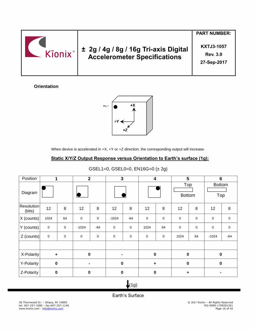
Orientation
When device is accelerated in +X, +Y or +Z direction, the corresponding output will increase.
Static X/Y/Z Output Response versus Orientation to Earth’s surface (1g):
GSEL1=0, GSEL0=0, EN16G=0 (± 2g)
Position 1 2 3 4 5 6
Diagram
Top
Bottom
Bottom
Top
Resolution (bits)
12 8 12 8 12 8 12 8 12 8 12 8
X (counts) 1024 64 0 0 -1024 -64 0 0 0 0 0 0
Y (counts) 0 0 -1024 -64 0 0 1024 64 0 0 0 0
Z (counts) 0 0 0 0 0 0 0 0 1024 64 -1024 -64
X-Polarity + 0 - 0 0 0
Y-Polarity 0 - 0 + 0 0
Z-Polarity 0 0 0 0 + -
(1g)
Earth’s Surface
± 2g / 4g / 8g / 16g Tri-axis Digital Accelerometer Specifications
PART NUMBER:
KXTJ3-1057
Rev. 3.0
27-Sep-2017
36 Thornwood Dr. – Ithaca, NY 14850 © 2017 Kionix – All Rights Reserved
tel: 607-257-1080 – fax:607-257-1146 762-9990-1709291201
www.kionix.com - [email protected] Page 17 of 42
Static X/Y/Z Output Response versus Orientation to Earth’s surface (1g):
GSEL1=0, GSEL0=1, EN16G =0 (± 4g)
Position 1 2 3 4 5 6
Diagram
Top
Bottom
Bottom
Top
Resolution (bits)
12 8 12 8 12 8 12 8 12 8 12 8
X (counts) 512 32 0 0 -512 -32 0 0 0 0 0 0
Y (counts) 0 0 -512 -32 0 0 512 32 0 0 0 0
Z (counts) 0 0 0 0 0 0 0 0 512 32 -512 -32
X-Polarity + 0 - 0 0 0
Y-Polarity 0 - 0 + 0 0
Z-Polarity 0 0 0 0 + -
(1g)
Earth’s Surface
± 2g / 4g / 8g / 16g Tri-axis Digital Accelerometer Specifications
PART NUMBER:
KXTJ3-1057
Rev. 3.0
27-Sep-2017
36 Thornwood Dr. – Ithaca, NY 14850 © 2017 Kionix – All Rights Reserved
tel: 607-257-1080 – fax:607-257-1146 762-9990-1709291201
www.kionix.com - [email protected] Page 18 of 42
Static X/Y/Z Output Response versus Orientation to Earth’s surface (1g):
GSEL1=1, GSEL0=0, EN16G =0 (± 8g) GSEL1=1, GSEL0=1, EN16G=0 (± 8g)1
Position 1 2 3 4 5 6
Diagram
Top
Bottom
Bottom
Top
Resolution (bits)
14 12 8 14 12 8 14 12 8 14 12 8 14 12 8 14 12 8
X(counts) 1024 256 16 0 0 0 -
1024 -
256 -
16 0 0 0 0 0 0 0 0 0
Y (counts) 0 0 0 -
1024 -
256 -
16 0 0 0 1024 256 16 0 0 0 0 0 0
Z(counts) 0 0 0 0 0 0 0 0 0 0 0 0 1024 256 16 -
1024 -
256 -
16
X-Polarity + 0 - 0 0 0
Y-Polarity 0 - 0 + 0 0
Z-Polarity 0 0 0 0 + -
(1g)
Earth’s Surface

± 2g / 4g / 8g / 16g Tri-axis Digital Accelerometer Specifications
PART NUMBER:
KXTJ3-1057
Rev. 3.0
27-Sep-2017
36 Thornwood Dr. – Ithaca, NY 14850 © 2017 Kionix – All Rights Reserved
tel: 607-257-1080 – fax:607-257-1146 762-9990-1709291201
www.kionix.com - [email protected] Page 19 of 42
Static X/Y/Z Output Response versus Orientation to Earth’s surface (1g):
GSEL1=0, GSEL0=0, EN16G =1 (± 16g) GSEL1=0, GSEL0=1, EN16G =1 (± 16g) GSEL1=1, GSEL0=0, EN16G =1 (± 16g) GSEL1=1, GSEL0=1, EN16G =1 (± 16g)1
Position 1 2 3 4 5 6
Diagram
Top
Bottom
Bottom
Top
Resolution (bits) 14 12 8 14 12 8 14 12 8 14 12 8 14 12 8 14 12 8
X(counts) 512 128 8 0 0 0 -512 -128 -8 0 0 0 0 0 0 0 0 0
Y (counts) 0 0 0 -512 -128 -8 0 0 0 512 128 8 0 0 0 0 0 0
Z(counts) 0 0 0 0 0 0 0 0 0 0 0 0 512 128 8 -512 -128 -8
X-Polarity + 0 - 0 0 0
Y-Polarity 0 - 0 + 0 0
Z-Polarity 0 0 0 0 + -
(1g)
Earth’s Surface Notes:
1. This is applicable for 14-bit mode only in High Resolution mode

± 2g / 4g / 8g / 16g Tri-axis Digital Accelerometer Specifications
PART NUMBER:
KXTJ3-1057
Rev. 3.0
27-Sep-2017
36 Thornwood Dr. – Ithaca, NY 14850 © 2017 Kionix – All Rights Reserved
tel: 607-257-1080 – fax:607-257-1146 762-9990-1709291201
www.kionix.com - [email protected] Page 20 of 42
Digital Interface The Kionix KXTJ3 digital accelerometer has the ability to communicate on the I2C digital serial interface bus. This allows for easy system integration by eliminating analog-to-digital converter requirements and by providing direct communication with system micro-controllers. The serial interface terms and descriptions as indicated in Table 6 will be observed throughout this document.
Term Description
Transmitter The device that transmits data to the bus.
Receiver The device that receives data from the bus.
Master The device that initiates a transfer, generates clock signals, and terminates a transfer.
Slave The device addressed by the Master.
Table 6: Serial Interface Terminologies
I2C Serial Interface As previously mentioned, the KXTJ3 has the ability to communicate on an I2C bus. I2C is primarily used for synchronous serial communication between a Master device and one or more Slave devices. The Master, typically a micro controller, provides the serial clock signal and addresses Slave devices on the bus. The KXTJ3 always operates as a Slave device during standard Master-Slave I2C operation. I2C is a two-wire serial interface that contains a Serial Clock (SCL) line and a Serial Data (SDA) line. SCL is a serial clock that is provided by the Master, but can be held low by any Slave device, putting the Master into a wait condition. SDA is a bi-directional line used to transmit and receive data to and from the interface. Data is transmitted MSB (Most Significant Bit) first in 8-bit per byte format, and the number of bytes transmitted per transfer is unlimited. The I2C bus is considered free when both lines are high. The I2C interface is compliant with high-speed mode, fast mode and standard mode I2C standards.
I2C Operation Transactions on the I2C bus begin after the Master transmits a start condition (S), which is defined as a high-to-low transition on the data line while the SCL line is held high. The bus is considered busy after this condition. The next byte of data transmitted after the start condition contains the Slave Address (SAD) in the seven MSBs (Most Significant Bits), and the LSB (Least Significant Bit) tells whether the Master will be receiving data ‘1’ from the Slave or transmitting data ‘0’ to the Slave. When a Slave Address is sent, each device on the bus compares the seven MSBs with its internally stored address. If they match, the device considers itself addressed by the Master. The KXTJ3’s Slave Address is comprised of a programmable part and a fixed part, which allows for connection of multiple KXTJ3's to
± 2g / 4g / 8g / 16g Tri-axis Digital Accelerometer Specifications
PART NUMBER:
KXTJ3-1057
Rev. 3.0
27-Sep-2017
36 Thornwood Dr. – Ithaca, NY 14850 © 2017 Kionix – All Rights Reserved
tel: 607-257-1080 – fax:607-257-1146 762-9990-1709291201
www.kionix.com - [email protected] Page 21 of 42
the same I2C bus. The Slave Address associated with the KXTJ3 is 000111X, where the programmable bit X is determined by the assignment of ADDR (pin 1) to GND or IO_VDD (Table 7). Also, Figure 2 shows how two KXTJ3's would be implemented on the same I2C bus. It is mandatory that receiving devices acknowledge (ACK) each transaction. Therefore, the transmitter must release the SDA line during this ACK pulse. The receiver then pulls the data line low so that it remains stable low during the high period of the ACK clock pulse. A receiver that has been addressed, whether it is Master or Slave, is obliged to generate an ACK after each byte of data has been received. To conclude a transaction, the Master must transmit a stop condition (P) by transitioning the SDA line from low to high while SCL is high. The I2C bus is now free. Note that if the KXTJ3 is accessed through I2C protocol before the startup is finished a NACK signal is sent.
Figure 2: Multiple KXTJ3 I2C Connection
Y X
Description Address
Pad 7-bit
Address Address <7> <6> <5> <4> <3> <2> <1> <0>
I2C Wr GND 0x0E 0x1C 0 0 0 1 1 1 0 0
I2C Rd GND 0x0E 0x1D 0 0 0 1 1 1 0 1
I2C Wr IO_VDD 0x0F 0x1E 0 0 0 1 1 1 1 0
I2C Rd IO_VDD 0x0F 0x1F 0 0 0 1 1 1 1 1
Table 7: I2C Slave Addresses for KXTJ3-1057

± 2g / 4g / 8g / 16g Tri-axis Digital Accelerometer Specifications
PART NUMBER:
KXTJ3-1057
Rev. 3.0
27-Sep-2017
36 Thornwood Dr. – Ithaca, NY 14850 © 2017 Kionix – All Rights Reserved
tel: 607-257-1080 – fax:607-257-1146 762-9990-1709291201
www.kionix.com - [email protected] Page 22 of 42
Writing to an 8-bit Register Upon power up, the Master must write to the KXTJ3’s control registers to set its operational mode. Therefore, when writing to a control register on the I2C bus, as shown Sequence 1 below, the following protocol must be observed: After a start condition, SAD+W transmission, and the KXTJ3 ACK has been returned, an 8-bit Register Address (RA) command is transmitted by the Master. This command is telling the KXTJ3 to which 8-bit register the Master will be writing the data. Since this is I2C mode, the MSB of the RA command should always be zero (0). The KXTJ3 acknowledges the RA and the Master transmits the data to be stored in the 8-bit register. The KXTJ3 acknowledges that it has received the data and the Master transmits a stop condition (P) to end the data transfer. The data sent to the KXTJ3 is now stored in the appropriate register. The KXTJ3 automatically increments the received RA commands and, therefore, multiple bytes of data can be written to sequential registers after each Slave ACK as shown in Sequence 2 on the following page. Note** If a STOP condition is sent on the least significant bit of write data or the following master acknowledge cycle, the last write operation is not guaranteed and it may alter the content of the affected registers.
Reading from an 8-bit Register When reading data from a KXTJ3 8-bit register on the I2C bus, as shown in Sequence 3 on the next page, the following protocol must be observed: The Master first transmits a start condition (S) and the appropriate Slave Address (SAD) with the LSB set at ‘0’ to write. The KXTJ3 acknowledges and the Master transmits the 8-bit RA of the register it wants to read. The KXTJ3 again acknowledges, and the Master transmits a repeated start condition (Sr). After the repeated start condition, the Master addresses the KXTJ3 with a ‘1’ in the LSB (SAD+R) to read from the previously selected register. The Slave then acknowledges and transmits the data from the requested register. The Master does not acknowledge (NACK) it received the transmitted data, but transmits a stop condition to end the data transfer. Note that the KXTJ3 automatically increments through its sequential registers, allowing data to be read from multiple registers following a single SAD+R command as shown below in Sequence 4. The 8-bit register data is transmitted using a left-most format, first bit shifted/clocked out being the MSB bit. If a receiver cannot transmit or receive another complete byte of data until it has performed some other function, it can hold SCL low to force the transmitter into a wait state. Data transfer only continues when the receiver is ready for another byte and releases SCL. Note** Accelerometer’s output data should be read in a single transaction using the auto-increment feature to prevent output data from being updated prior to intended completion of the read transaction.

± 2g / 4g / 8g / 16g Tri-axis Digital Accelerometer Specifications
PART NUMBER:
KXTJ3-1057
Rev. 3.0
27-Sep-2017
36 Thornwood Dr. – Ithaca, NY 14850 © 2017 Kionix – All Rights Reserved
tel: 607-257-1080 – fax:607-257-1146 762-9990-1709291201
www.kionix.com - [email protected] Page 23 of 42
Data Transfer Sequences The following information clearly illustrates the variety of data transfers that can occur on the I2C bus and how the Master and Slave interact during these transfers. Table 8 defines the I2C terms used during the data transfers.
Term Definition
S Start Condition
Sr Repeated Start Condition
SAD Slave Address
W Write Bit
R Read Bit
ACK Acknowledge
NACK Not Acknowledge
RA Register Address
Data Transmitted/Received Data
P Stop Condition
Table 8: I2C Terms Sequence 1: The Master is writing one byte to the Slave.
Master S SAD + W RA DATA P
Slave ACK ACK ACK
Sequence 2: The Master is writing multiple bytes to the Slave.
Master S SAD + W RA DATA DATA P
Slave ACK ACK ACK ACK
Sequence 3: The Master is receiving one byte of data from the Slave.
Master S SAD + W RA Sr SAD + R NACK P
Slave ACK ACK ACK DATA
Sequence 4: The Master is receiving multiple bytes of data from the Slave.
Master S SAD + W RA Sr SAD + R ACK NACK P
Slave ACK ACK ACK DATA DATA

± 2g / 4g / 8g / 16g Tri-axis Digital Accelerometer Specifications
PART NUMBER:
KXTJ3-1057
Rev. 3.0
27-Sep-2017
36 Thornwood Dr. – Ithaca, NY 14850 © 2017 Kionix – All Rights Reserved
tel: 607-257-1080 – fax:607-257-1146 762-9990-1709291201
www.kionix.com - [email protected] Page 24 of 42
HS-mode To enter the 3.4MHz high speed mode of communication, the device must receive the following sequence of conditions from the master: a Start condition followed by a Master code (00001XXX) and a Master Non-acknowledge. Once recognized, the device switches to HS-mode communication. Read/write data transfers then proceed as described in the sequences above. Devices return to the FS-mode after a STOP occurrence on the bus. Sequence 5: HS-mode data transfer of the Master writing multiple bytes to the Slave.
Speed FS-mode HS-mode FS-mode
Master S M-code NACK Sr SAD + W RA DATA P
Slave ACK ACK ACK
Sequence 6: HS-mode data transfer of the Master receiving multiple bytes of data from the Slave.
Speed FS-mode HS-mode
Master S M-code NACK Sr SAD + W RA
Slave ACK ACK
Speed HS-mode FS-mode
Master Sr SAD + R NACK P
Slave ACK DATA ACK DATA
n bytes + ack.
(n-1) bytes + ack.

± 2g / 4g / 8g / 16g Tri-axis Digital Accelerometer Specifications
PART NUMBER:
KXTJ3-1057
Rev. 3.0
27-Sep-2017
36 Thornwood Dr. – Ithaca, NY 14850 © 2017 Kionix – All Rights Reserved
tel: 607-257-1080 – fax:607-257-1146 762-9990-1709291201
www.kionix.com - [email protected] Page 25 of 42
I2C Timing Diagram
Number Description MIN MAX Units
t0 SDA low to SCL low transition (Start event) 50
- ns t1 SDA low to first SCL rising edge 100
- ns
t2 SCL pulse width: high 100
- ns
t3 SCL pulse width: low 100
- ns
t4 SCL high before SDA falling edge (Start Repeated) 50
- ns
t5 SCL pulse width: high during a S/Sr/P event 100
- ns
t6 SCL high before SDA rising edge (Stop) 50
- ns
t7 SDA pulse width: high 25
- ns
t8 SDA valid to SCL rising edge 50
- ns
t9 SCL rising edge to SDA invalid 50
- ns
t10 SCL falling edge to SDA valid (when slave is transmitting) - 100
ns
t11 SCL falling edge to SDA invalid (when slave is transmitting) 0
- ns
Note Recommended I2C CLK 2.5
- us Table 9: I2C Timing (Fast Mode)
± 2g / 4g / 8g / 16g Tri-axis Digital Accelerometer Specifications
PART NUMBER:
KXTJ3-1057
Rev. 3.0
27-Sep-2017
36 Thornwood Dr. – Ithaca, NY 14850 © 2017 Kionix – All Rights Reserved
tel: 607-257-1080 – fax:607-257-1146 762-9990-1709291201
www.kionix.com - [email protected] Page 26 of 42
Embedded Registers
The KXTJ3 has 20 embedded 8-bit registers that are accessible by the user. This section contains the addresses for all embedded registers and also describes bit functions of each register.
Register Name Type (R/W) Register Address (Hex)
Kionix Reserved - 0x00 – 0x05
XOUT_L R 0x06
XOUT_H R 0x07
YOUT_L R 0x08
YOUT_H R 0x09
ZOUT_L R 0x0A
ZOUT_H R 0x0B
DCST_RESP R 0x0C
Kionix Reserved - 0x0D – 0x0E
WHO_AM_I R 0x0F
Kionix Reserved - 0x10 – 0 x15
INT_SOURCE1 R 0x16
INT_SOURCE2 R 0x17
STATUS_REG R 0x18
Kionix Reserved - 0x19
INT_REL R 0x1A
CTRL_REG1* R/W 0x1B
Kionix Reserved - 0x1C
CTRL_REG2* R/W 0x1D
INT_CTRL_REG1* R/W 0x1E
INT_CTRL_REG2* R/W 0x1F
Kionix Reserved - 0x20
DATA_CTRL_REG* R/W 0x21
Kionix Reserved - 0x22 – 0x28
WAKEUP_COUNTER* R/W 0x29
NA_COUNTER* R/W 0x2A
Kionix Reserved - 0x2B – 0x39
SELF_TEST* W 0x3A
Kionix Reserved - 0x3B – 0x69
WAKEUP_THRESHOLD_H* R/W 0x6A
WAKEUP_THRESHOLD_H* R/W 0x6B
Table 10: Register Map
* Note: When changing the contents of these registers, the PC1 bit in CTRL_REG1 must first be set to “0”
± 2g / 4g / 8g / 16g Tri-axis Digital Accelerometer Specifications
PART NUMBER:
KXTJ3-1057
Rev. 3.0
27-Sep-2017
36 Thornwood Dr. – Ithaca, NY 14850 © 2017 Kionix – All Rights Reserved
tel: 607-257-1080 – fax:607-257-1146 762-9990-1709291201
www.kionix.com - [email protected] Page 27 of 42
Register Descriptions
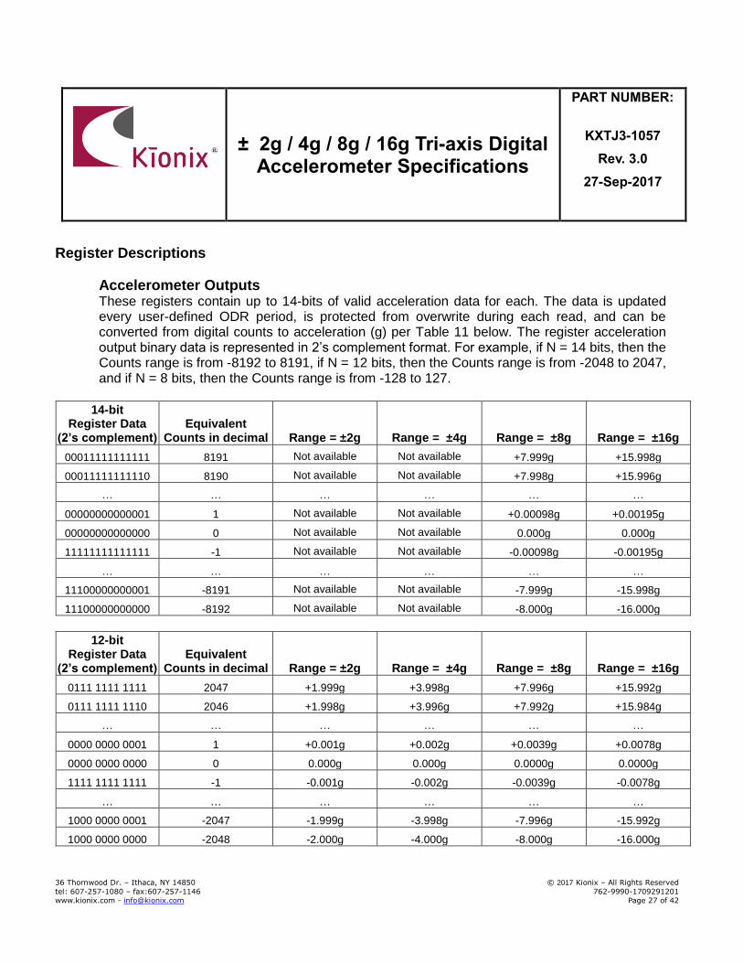
Accelerometer Outputs These registers contain up to 14-bits of valid acceleration data for each. The data is updated every user-defined ODR period, is protected from overwrite during each read, and can be converted from digital counts to acceleration (g) per Table 11 below. The register acceleration output binary data is represented in 2’s complement format. For example, if N = 14 bits, then the Counts range is from -8192 to 8191, if N = 12 bits, then the Counts range is from -2048 to 2047, and if N = 8 bits, then the Counts range is from -128 to 127.
14-bit Register Data
(2’s complement) Equivalent
Counts in decimal Range = ±2g Range = ±4g Range = ±8g Range = ±16g
00011111111111 8191 Not available Not available +7.999g +15.998g
00011111111110 8190 Not available Not available +7.998g +15.996g
… … … … … …
00000000000001 1 Not available Not available +0.00098g +0.00195g
00000000000000 0 Not available Not available 0.000g 0.000g
11111111111111 -1 Not available Not available -0.00098g -0.00195g
… … … … … …
11100000000001 -8191 Not available Not available -7.999g -15.998g
11100000000000 -8192 Not available Not available -8.000g -16.000g
12-bit Register Data
(2’s complement) Equivalent
Counts in decimal Range = ±2g Range = ±4g Range = ±8g Range = ±16g
0111 1111 1111 2047 +1.999g +3.998g +7.996g +15.992g
0111 1111 1110 2046 +1.998g +3.996g +7.992g +15.984g
… … … … … …
0000 0000 0001 1 +0.001g +0.002g +0.0039g +0.0078g
0000 0000 0000 0 0.000g 0.000g 0.0000g 0.0000g
1111 1111 1111 -1 -0.001g -0.002g -0.0039g -0.0078g
… … … … … …
1000 0000 0001 -2047 -1.999g -3.998g -7.996g -15.992g
1000 0000 0000 -2048 -2.000g -4.000g -8.000g -16.000g
± 2g / 4g / 8g / 16g Tri-axis Digital Accelerometer Specifications
PART NUMBER:
KXTJ3-1057
Rev. 3.0
27-Sep-2017
36 Thornwood Dr. – Ithaca, NY 14850 © 2017 Kionix – All Rights Reserved
tel: 607-257-1080 – fax:607-257-1146 762-9990-1709291201
www.kionix.com - [email protected] Page 28 of 42
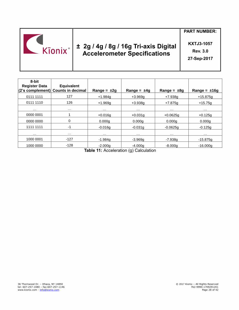
8-bit Register Data
(2’s complement)
Equivalent
Counts in decimal Range = ±2g Range = ±4g Range = ±8g Range = ±16g
0111 1111 127 +1.984g +3.969g +7.938g +15.875g
0111 1110 126 +1.969g +3.938g +7.875g +15.75g
… … … … … …
0000 0001 1 +0.016g +0.031g +0.0625g +0.125g
0000 0000 0 0.000g 0.000g 0.000g 0.000g
1111 1111 -1 -0.016g -0.031g -0.0625g -0.125g
… … … … … …
1000 0001 -127 -1.984g -3.969g -7.938g -15.875g
1000 0000 -128 -2.000g -4.000g -8.000g -16.000g
Table 11: Acceleration (g) Calculation

± 2g / 4g / 8g / 16g Tri-axis Digital Accelerometer Specifications
PART NUMBER:
KXTJ3-1057
Rev. 3.0
27-Sep-2017
36 Thornwood Dr. – Ithaca, NY 14850 © 2017 Kionix – All Rights Reserved
tel: 607-257-1080 – fax:607-257-1146 762-9990-1709291201
www.kionix.com - [email protected] Page 29 of 42
XOUT_L X-axis accelerometer output least significant byte
R R R R R R R R Resolution
XOUTD5 XOUTD4 XOUTD3 XOUTD2 XOUTD1 XOUTD0 X X 14-bit
XOUTD3 XOUTD2 XOUTD1 XOUTD0 X X X X 12-bit
X X X X X X X X 8-bit
Bit7 Bit6 Bit5 Bit4 Bit3 Bit2 Bit1 Bit0
I2C Address: 0x06
XOUT_H X-axis accelerometer output most significant byte
R R R R R R R R Resolution
XOUTD13 XOUTD12 XOUTD11 XOUTD10 XOUTD9 XOUTD8 XOUTD7 XOUTD6 14-bit
XOUTD11 XOUTD10 XOUTD9 XOUTD8 XOUTD7 XOUTD6 XOUTD5 XOUTD4 12-bit
XOUTD7 XOUTD6 XOUTD5 XOUTD4 XOUTD3 XOUTD2 XOUTD1 XOUTD0 8-bit
Bit7 Bit6 Bit5 Bit4 Bit3 Bit2 Bit1 Bit0
I2C Address: 0x07
YOUT_L Y-axis accelerometer output least significant byte
R R R R R R R R Resolution
YOUTD5 YOUTD4 YOUTD3 YOUTD2 YOUTD1 YOUTD0 Y Y 14-bit
YOUTD3 YOUTD2 YOUTD1 YOUTD0 X X X X 12-bit
X X X X X X X X 8-bit
Bit7 Bit6 Bit5 Bit4 Bit3 Bit2 Bit1 Bit0
I2C Address: 0x08
YOUT_H Y-axis accelerometer output most significant byte
R R R R R R R R Resolution
YOUTD13 YOUTD12 YOUTD11 YOUTD10 YOUTD9 YOUTD8 YOUTD7 YOUTD6 14-bit
YOUTD11 YOUTD10 YOUTD9 YOUTD8 YOUTD7 YOUTD6 YOUTD5 YOUTD4 12-bit
YOUTD7 YOUTD6 YOUTD5 YOUTD4 YOUTD3 YOUTD2 YOUTD1 YOUTD0 8-bit
Bit7 Bit6 Bit5 Bit4 Bit3 Bit2 Bit1 Bit0
I2C Address: 0x09
± 2g / 4g / 8g / 16g Tri-axis Digital Accelerometer Specifications
PART NUMBER:
KXTJ3-1057
Rev. 3.0
27-Sep-2017
36 Thornwood Dr. – Ithaca, NY 14850 © 2017 Kionix – All Rights Reserved
tel: 607-257-1080 – fax:607-257-1146 762-9990-1709291201
www.kionix.com - [email protected] Page 30 of 42
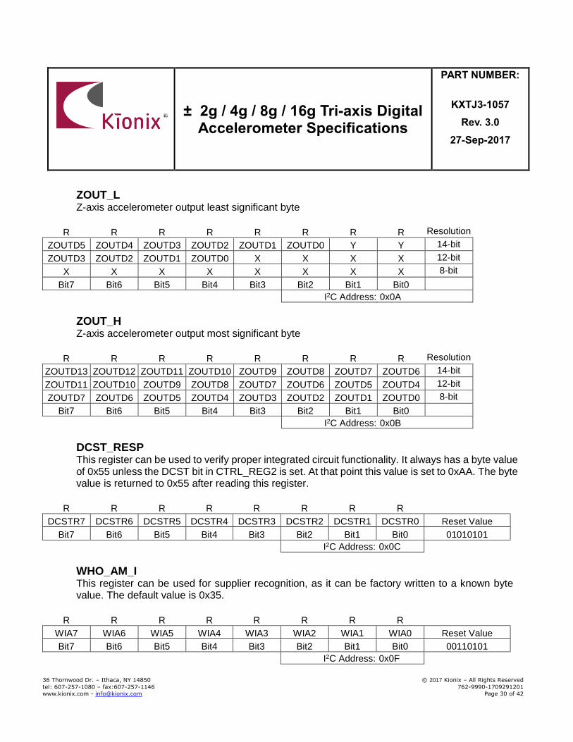
ZOUT_L Z-axis accelerometer output least significant byte
R R R R R R R R Resolution
ZOUTD5 ZOUTD4 ZOUTD3 ZOUTD2 ZOUTD1 ZOUTD0 Y Y 14-bit
ZOUTD3 ZOUTD2 ZOUTD1 ZOUTD0 X X X X 12-bit
X X X X X X X X 8-bit
Bit7 Bit6 Bit5 Bit4 Bit3 Bit2 Bit1 Bit0
I2C Address: 0x0A
ZOUT_H Z-axis accelerometer output most significant byte
R R R R R R R R Resolution
ZOUTD13 ZOUTD12 ZOUTD11 ZOUTD10 ZOUTD9 ZOUTD8 ZOUTD7 ZOUTD6 14-bit
ZOUTD11 ZOUTD10 ZOUTD9 ZOUTD8 ZOUTD7 ZOUTD6 ZOUTD5 ZOUTD4 12-bit
ZOUTD7 ZOUTD6 ZOUTD5 ZOUTD4 ZOUTD3 ZOUTD2 ZOUTD1 ZOUTD0 8-bit
Bit7 Bit6 Bit5 Bit4 Bit3 Bit2 Bit1 Bit0
I2C Address: 0x0B
DCST_RESP This register can be used to verify proper integrated circuit functionality. It always has a byte value of 0x55 unless the DCST bit in CTRL_REG2 is set. At that point this value is set to 0xAA. The byte value is returned to 0x55 after reading this register.
R R R R R R R R
DCSTR7 DCSTR6 DCSTR5 DCSTR4 DCSTR3 DCSTR2 DCSTR1 DCSTR0 Reset Value
Bit7 Bit6 Bit5 Bit4 Bit3 Bit2 Bit1 Bit0 01010101
I2C Address: 0x0C
WHO_AM_I This register can be used for supplier recognition, as it can be factory written to a known byte value. The default value is 0x35.
R R R R R R R R
WIA7 WIA6 WIA5 WIA4 WIA3 WIA2 WIA1 WIA0 Reset Value
Bit7 Bit6 Bit5 Bit4 Bit3 Bit2 Bit1 Bit0 00110101
I2C Address: 0x0F

± 2g / 4g / 8g / 16g Tri-axis Digital Accelerometer Specifications
PART NUMBER:
KXTJ3-1057
Rev. 3.0
27-Sep-2017
36 Thornwood Dr. – Ithaca, NY 14850 © 2017 Kionix – All Rights Reserved
tel: 607-257-1080 – fax:607-257-1146 762-9990-1709291201
www.kionix.com - [email protected] Page 31 of 42
Interrupt Source Registers
These two registers report interrupt state changes. This data is updated when a new interrupt event occurs and each application’s result is latched until the interrupt release register is read. The programmable interrupt engine can be configured to report data in an unlatched manner via the interrupt control registers.
INT_SOURCE1 This register reports which function caused an interrupt. Reading from the interrupt release register (INT_REL, 0x1A) will clear the entire contents of this register.
R R R R R R R R
0 0 0 DRDY 0 0 WUFS 0
Bit7 Bit6 Bit5 Bit4 Bit3 Bit2 Bit1 Bit0
I2C Address: 0x16
DRDY - indicates that new acceleration data (at Reg Addr 0x06 to 0x0B) is available.
This bit is cleared when acceleration data is read or the interrupt release register (INT_REL, 0x1A) is read.
0 = New acceleration data not available 1 = New acceleration data available WUFS - Wake up has occurred. This bit is cleared when the interrupt source latch
register (INT_REL, 0x1A) is read. 0 = No motion 1 = Motion has activated the interrupt
INT_SOURCE2 This register reports the axis and direction of detected motion per Table 12. This register is cleared when the interrupt source latch register (INT_REL, 0x1A is read.
R R R R R R R R
0 0 XNWU XPWU YNWU YPWU ZNWU ZPWU
Bit7 Bit6 Bit5 Bit4 Bit3 Bit2 Bit1 Bit0
I2C Address: 0x17
± 2g / 4g / 8g / 16g Tri-axis Digital Accelerometer Specifications
PART NUMBER:
KXTJ3-1057
Rev. 3.0
27-Sep-2017
36 Thornwood Dr. – Ithaca, NY 14850 © 2017 Kionix – All Rights Reserved
tel: 607-257-1080 – fax:607-257-1146 762-9990-1709291201
www.kionix.com - [email protected] Page 32 of 42
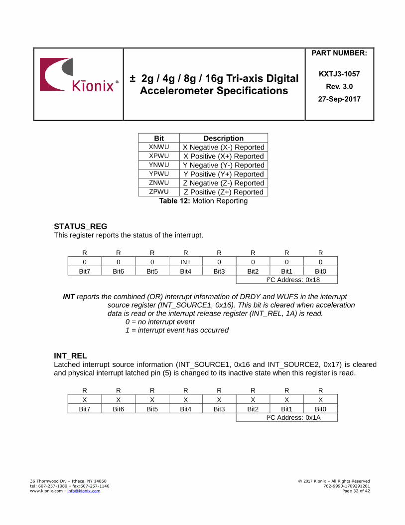
Bit Description XNWU X Negative (X-) Reported XPWU X Positive (X+) Reported YNWU Y Negative (Y-) Reported YPWU Y Positive (Y+) Reported ZNWU Z Negative (Z-) Reported ZPWU Z Positive (Z+) Reported
Table 12: Motion Reporting
STATUS_REG This register reports the status of the interrupt.
R R R R R R R R
0 0 0 INT 0 0 0 0
Bit7 Bit6 Bit5 Bit4 Bit3 Bit2 Bit1 Bit0
I2C Address: 0x18
INT reports the combined (OR) interrupt information of DRDY and WUFS in the interrupt
source register (INT_SOURCE1, 0x16). This bit is cleared when acceleration data is read or the interrupt release register (INT_REL, 1A) is read.
0 = no interrupt event 1 = interrupt event has occurred
INT_REL Latched interrupt source information (INT_SOURCE1, 0x16 and INT_SOURCE2, 0x17) is cleared and physical interrupt latched pin (5) is changed to its inactive state when this register is read.
R R R R R R R R
X X X X X X X X
Bit7 Bit6 Bit5 Bit4 Bit3 Bit2 Bit1 Bit0
I2C Address: 0x1A
± 2g / 4g / 8g / 16g Tri-axis Digital Accelerometer Specifications
PART NUMBER:
KXTJ3-1057
Rev. 3.0
27-Sep-2017
36 Thornwood Dr. – Ithaca, NY 14850 © 2017 Kionix – All Rights Reserved
tel: 607-257-1080 – fax:607-257-1146 762-9990-1709291201
www.kionix.com - [email protected] Page 33 of 42
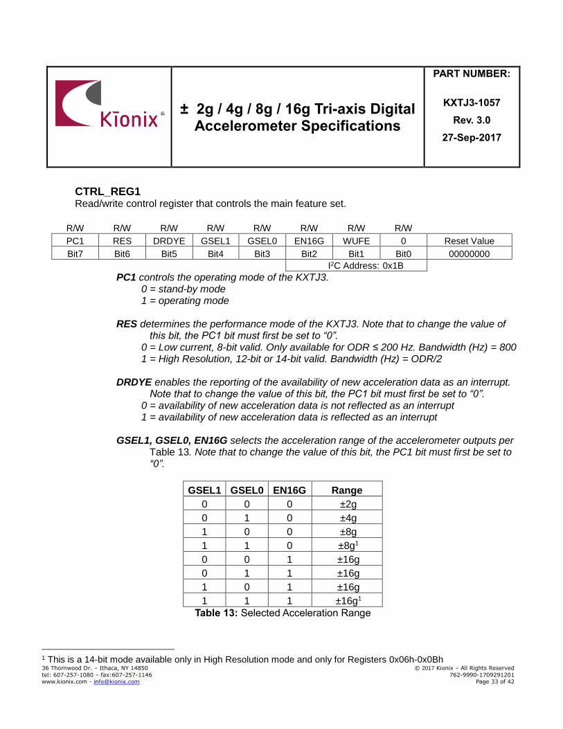
CTRL_REG1 Read/write control register that controls the main feature set.
R/W R/W R/W R/W R/W R/W R/W R/W
PC1 RES DRDYE GSEL1 GSEL0 EN16G WUFE 0 Reset Value
Bit7 Bit6 Bit5 Bit4 Bit3 Bit2 Bit1 Bit0 00000000
I2C Address: 0x1B
PC1 controls the operating mode of the KXTJ3. 0 = stand-by mode 1 = operating mode
RES determines the performance mode of the KXTJ3. Note that to change the value of this bit, the PC1 bit must first be set to “0”.
0 = Low current, 8-bit valid. Only available for ODR ≤ 200 Hz. Bandwidth (Hz) = 800 1 = High Resolution, 12-bit or 14-bit valid. Bandwidth (Hz) = ODR/2
DRDYE enables the reporting of the availability of new acceleration data as an interrupt.
Note that to change the value of this bit, the PC1 bit must first be set to “0”. 0 = availability of new acceleration data is not reflected as an interrupt 1 = availability of new acceleration data is reflected as an interrupt
GSEL1, GSEL0, EN16G selects the acceleration range of the accelerometer outputs per Table 13. Note that to change the value of this bit, the PC1 bit must first be set to “0”.
GSEL1 GSEL0 EN16G Range
0 0 0 ±2g
0 1 0 ±4g
1 0 0 ±8g
1 1 0 ±8g1
0 0 1 ±16g
0 1 1 ±16g
1 0 1 ±16g
1 1 1 ±16g1
Table 13: Selected Acceleration Range
1 This is a 14-bit mode available only in High Resolution mode and only for Registers 0x06h-0x0Bh
± 2g / 4g / 8g / 16g Tri-axis Digital Accelerometer Specifications
PART NUMBER:
KXTJ3-1057
Rev. 3.0
27-Sep-2017
36 Thornwood Dr. – Ithaca, NY 14850 © 2017 Kionix – All Rights Reserved
tel: 607-257-1080 – fax:607-257-1146 762-9990-1709291201
www.kionix.com - [email protected] Page 34 of 42
WUFE enables the Wake Up (motion detect) function. 0=disabled, 1=enabled. Note that to change the value of this bit, the PC1 bit must first be set to “0”.
0 = Wake Up function disabled 1 = Wake Up function enabled
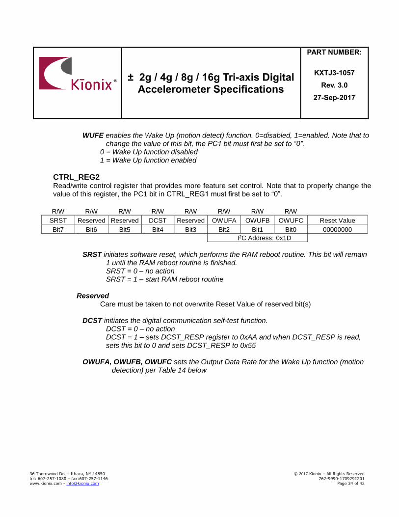
CTRL_REG2 Read/write control register that provides more feature set control. Note that to properly change the value of this register, the PC1 bit in CTRL_REG1 must first be set to “0”.
R/W R/W R/W R/W R/W R/W R/W R/W
SRST Reserved Reserved DCST Reserved OWUFA OWUFB OWUFC Reset Value
Bit7 Bit6 Bit5 Bit4 Bit3 Bit2 Bit1 Bit0 00000000
I2C Address: 0x1D
SRST initiates software reset, which performs the RAM reboot routine. This bit will remain
1 until the RAM reboot routine is finished. SRST = 0 – no action SRST = 1 – start RAM reboot routine
Reserved Care must be taken to not overwrite Reset Value of reserved bit(s)
DCST initiates the digital communication self-test function. DCST = 0 – no action DCST = 1 – sets DCST_RESP register to 0xAA and when DCST_RESP is read,
sets this bit to 0 and sets DCST_RESP to 0x55
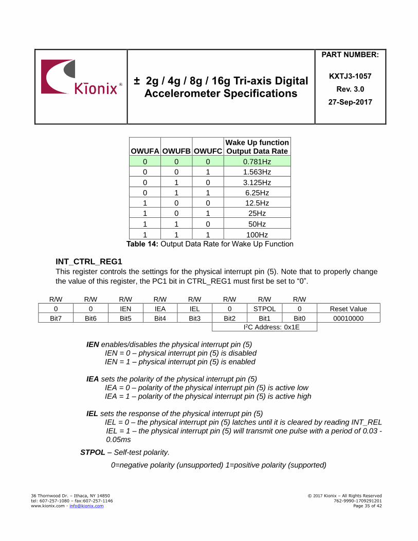
OWUFA, OWUFB, OWUFC sets the Output Data Rate for the Wake Up function (motion detection) per Table 14 below
± 2g / 4g / 8g / 16g Tri-axis Digital Accelerometer Specifications
PART NUMBER:
KXTJ3-1057
Rev. 3.0
27-Sep-2017
36 Thornwood Dr. – Ithaca, NY 14850 © 2017 Kionix – All Rights Reserved
tel: 607-257-1080 – fax:607-257-1146 762-9990-1709291201
www.kionix.com - [email protected] Page 35 of 42
OWUFA OWUFB OWUFC Wake Up function Output Data Rate
0 0 0 0.781Hz
0 0 1 1.563Hz
0 1 0 3.125Hz
0 1 1 6.25Hz
1 0 0 12.5Hz
1 0 1 25Hz
1 1 0 50Hz
1 1 1 100Hz
Table 14: Output Data Rate for Wake Up Function
INT_CTRL_REG1
This register controls the settings for the physical interrupt pin (5). Note that to properly change
the value of this register, the PC1 bit in CTRL_REG1 must first be set to “0”.
R/W R/W R/W R/W R/W R/W R/W R/W
0 0 IEN IEA IEL 0 STPOL 0 Reset Value
Bit7 Bit6 Bit5 Bit4 Bit3 Bit2 Bit1 Bit0 00010000
I2C Address: 0x1E
IEN enables/disables the physical interrupt pin (5) IEN = 0 – physical interrupt pin (5) is disabled IEN = 1 – physical interrupt pin (5) is enabled IEA sets the polarity of the physical interrupt pin (5) IEA = 0 – polarity of the physical interrupt pin (5) is active low IEA = 1 – polarity of the physical interrupt pin (5) is active high IEL sets the response of the physical interrupt pin (5) IEL = 0 – the physical interrupt pin (5) latches until it is cleared by reading INT_REL
IEL = 1 – the physical interrupt pin (5) will transmit one pulse with a period of 0.03 - 0.05ms
STPOL – Self-test polarity.
0=negative polarity (unsupported) 1=positive polarity (supported)

± 2g / 4g / 8g / 16g Tri-axis Digital Accelerometer Specifications
PART NUMBER:
KXTJ3-1057
Rev. 3.0
27-Sep-2017
36 Thornwood Dr. – Ithaca, NY 14850 © 2017 Kionix – All Rights Reserved
tel: 607-257-1080 – fax:607-257-1146 762-9990-1709291201
www.kionix.com - [email protected] Page 36 of 42
INT_CTRL_REG2
This register controls which axis and direction of detected motion can cause an interrupt. Note that to
properly change the value of this register, the PC1 bit in CTRL_REG1 must first be set to “0”.
R/W R/W R/W R/W R/W R/W R/W R/W
ULMODE 0 XNWUE XPWUE YNWUE YPWUE ZNWUE ZPWUE Reset Value
Bit7 Bit6 Bit5 Bit4 Bit3 Bit2 Bit1 Bit0 00111111
I2C Address: 0x1F
ULMODE – Unlatched mode motion interrupt, 0=disable, 1=enable XNWU - x negative (x-): 0 = disabled, 1 = enabled XPWU - x positive (x+): 0 = disabled, 1 = enabled YNWU - y negative (y-): 0 = disabled, 1 = enabled YPWU - y positive (y+): 0 = disabled, 1 = enabled ZNWU - z negative (z-): 0 = disabled, 1 = enabled ZPWU - z positive (z+): 0 = disabled, 1 = enabled
DATA_CTRL_REG Read/write control register that configures the acceleration outputs. Note that to properly change the value of this register, the PC1 bit in CTRL_REG1 must first be set to “0”.
R/W R/W R/W R/W R/W R/W R/W R/W
0 0 0 0 OSAA OSAB OSAC OSAD Reset Value
Bit7 Bit6 Bit5 Bit4 Bit3 Bit2 Bit1 Bit0 00000010
I2C Address: 0x21
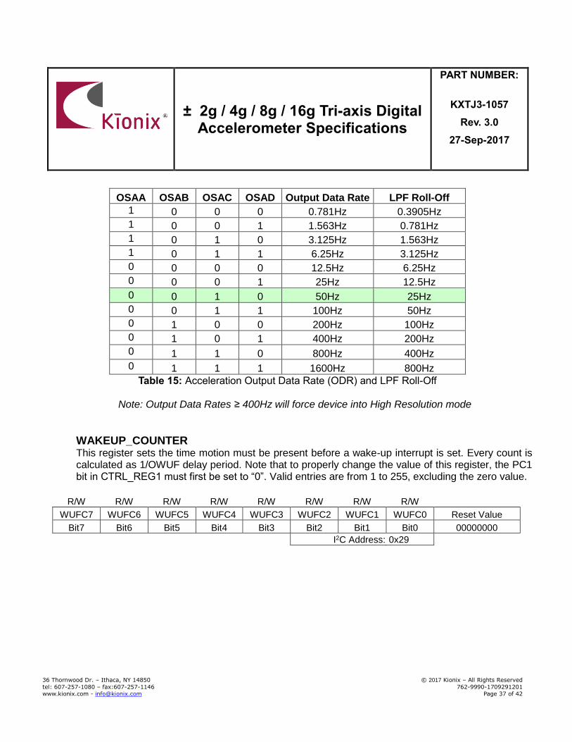
OSAA, OSAB, OSAC, OSAD sets the output data rate (ODR) for the low-pass filtered acceleration
outputs per Table 15.
± 2g / 4g / 8g / 16g Tri-axis Digital Accelerometer Specifications
PART NUMBER:
KXTJ3-1057
Rev. 3.0
27-Sep-2017
36 Thornwood Dr. – Ithaca, NY 14850 © 2017 Kionix – All Rights Reserved
tel: 607-257-1080 – fax:607-257-1146 762-9990-1709291201
www.kionix.com - [email protected] Page 37 of 42
OSAA OSAB OSAC OSAD Output Data Rate LPF Roll-Off
1 0 0 0 0.781Hz 0.3905Hz
1 0 0 1 1.563Hz 0.781Hz
1 0 1 0 3.125Hz 1.563Hz
1 0 1 1 6.25Hz 3.125Hz
0 0 0 0 12.5Hz 6.25Hz
0 0 0 1 25Hz 12.5Hz
0 0 1 0 50Hz 25Hz
0 0 1 1 100Hz 50Hz
0 1 0 0 200Hz 100Hz
0 1 0 1 400Hz 200Hz
0 1 1 0 800Hz 400Hz
0 1 1 1 1600Hz 800Hz
Table 15: Acceleration Output Data Rate (ODR) and LPF Roll-Off
Note: Output Data Rates ≥ 400Hz will force device into High Resolution mode
WAKEUP_COUNTER This register sets the time motion must be present before a wake-up interrupt is set. Every count is calculated as 1/OWUF delay period. Note that to properly change the value of this register, the PC1 bit in CTRL_REG1 must first be set to “0”. Valid entries are from 1 to 255, excluding the zero value.
R/W R/W R/W R/W R/W R/W R/W R/W
WUFC7 WUFC6 WUFC5 WUFC4 WUFC3 WUFC2 WUFC1 WUFC0 Reset Value
Bit7 Bit6 Bit5 Bit4 Bit3 Bit2 Bit1 Bit0 00000000
I2C Address: 0x29

± 2g / 4g / 8g / 16g Tri-axis Digital Accelerometer Specifications
PART NUMBER:
KXTJ3-1057
Rev. 3.0
27-Sep-2017
36 Thornwood Dr. – Ithaca, NY 14850 © 2017 Kionix – All Rights Reserved
tel: 607-257-1080 – fax:607-257-1146 762-9990-1709291201
www.kionix.com - [email protected] Page 38 of 42
NA_COUNTER This register sets the non-activity time required before another wake-up interrupt can be set. Every count is calculated as 1/OWUF delay period. Note that to properly change the value of this register, the PC1 bit in CTRL_REG1 must first be set to “0”. Valid entries are from 1 to 255, excluding the zero value.
R/W R/W R/W R/W R/W R/W R/W R/W
NAFC7 NAFC6 NAFC5 NAFC4 NAFC3 NAFC2 NAFC1 NAFC0 Reset Value
Bit7 Bit6 Bit5 Bit4 Bit3 Bit2 Bit1 Bit0 00000000
I2C Address: 0x2A
SELF_TEST When 0xCA is written to this register, the MEMS self-test function is enabled. Electrostatic-actuation of the accelerometer, results in a DC shift of the X, Y and Z axis outputs. Writing 0x00 to this register will return the accelerometer to normal operation.
WAKEUP_THRESHOLD This register sets the threshold for wake-up (motion detect) interrupt is set. Data bytes are WAKEUP_THRESHOLD_H, WAKEUP_THRESHOLD_L. The KXTJ3 will be shipped from the factory with this value set to correspond to a change in acceleration of 0.5g (3.9mg/count). Note that to properly change the value of this register, the PC1 bit in CTRL_REG1 must first be set to “0”.
R/W R/W R/W R/W R/W R/W R/W R/W Reset Value
WUTH11 WUTH10 WUTH9 WUTH8 WUTH7 WUTH6 WUTH5 WUTH4 00001000
WUTH3 WUTH2 WUTH1 WUTH0 0 0 0 0 00000000
Bit7 Bit6 Bit5 Bit4 Bit3 Bit2 Bit1 Bit0
I2C Address: 0x6A – 0x6B
W W W W W W W W
0 0 0 0 0 0 0 0 Reset Value
Bit7 Bit6 Bit5 Bit4 Bit3 Bit2 Bit1 Bit0 00000000
I2C Address: 0x3A

± 2g / 4g / 8g / 16g Tri-axis Digital Accelerometer Specifications
PART NUMBER:
KXTJ3-1057
Rev. 3.0
27-Sep-2017
36 Thornwood Dr. – Ithaca, NY 14850 © 2017 Kionix – All Rights Reserved
tel: 607-257-1080 – fax:607-257-1146 762-9990-1709291201
www.kionix.com - [email protected] Page 39 of 42
Embedded Wake Up Function The motion interrupt feature of the KXTJ3 reports qualified changes in the high-pass filtered acceleration based on the WAKEUP_THRESHOLD. If the high-pass filtered acceleration on any axis is greater than the user-defined WAKEUP_THRESHOLD, the device has transitioned from an inactive state to an active state. Equation 1 and Equation 2 show how to calculate the engine threshold (WAKEUP_THRESHOLD) and delay time (WAKEUP_COUNTER) register values for the desired result.
WAKEUP_THRESHOLD (counts) = Desired Threshold (g) x 256 (counts/g)
Equation 1: Wake Up Threshold
An 8-bit raw unsigned value represents a counter that permits the user to qualify each active/inactive state change. Note that each WAKEUP_COUNTER count qualifies 1 (one) user-defined ODR period (OWUF). Equation 2 shows how to calculate the WAKEUP_COUNTER register value for a desired wake up delay time.
WAKEUP_COUNTER (counts) = Desired Delay Time (sec) x OWUF (Hz)
Equation 2: Wake Up Delay Time The latched motion interrupt response algorithm works as following: while the part is in inactive state, the algorithm evaluates differential measurement between each new acceleration data point with the preceding one and evaluates it against the WAKEUP_THRESHOLD threshold. When the differential measurement is greater than WAKEUP_THRESHOLD threshold, the wakeup counter starts the count. Differential measurements are now calculated based on the difference between the current acceleration and the acceleration when the counter started. The part will report that motion has occurred at the end of the count assuming each differential measurement has remained above the threshold. If at any moment during the count the differential measurement falls below the threshold, the counter will stop the count and the part will remain in inactive state. To illustrate how the algorithm works, consider the Figure 3 below that shows the latched response of the motion detection algorithm with WAKEUP_COUNTER set to 10 counts. Note how the difference between the acceleration sample marked in red and the one marked in green resulted in a differential measurements represented with orange bar being above the WAKEUP_THRESHOLD. At this point, the counter begins to count number of counts stored in WAKEUP_COUNTER register and the wakeup algorithm will evaluate the difference between each new acceleration measurement and the measurement marked in green that will remain a reference measurement for the duration of the counter count. At the end of the count, assuming all differential measurements were larger than WAKEUP_THRESHOLD, as is the case in the example showed in Figure 3, a motion event will be reported.

± 2g / 4g / 8g / 16g Tri-axis Digital Accelerometer Specifications
PART NUMBER:
KXTJ3-1057
Rev. 3.0
27-Sep-2017
36 Thornwood Dr. – Ithaca, NY 14850 © 2017 Kionix – All Rights Reserved
tel: 607-257-1080 – fax:607-257-1146 762-9990-1709291201
www.kionix.com - [email protected] Page 40 of 42
Figure 3 below shows the latched response of the Wake Up Function with WUF counter = 10 counts.
Figure 3: Latched Motion Interrupt Response
The KXTJ3 wake-up function is always latched unless ULMODE = 1. If ULMODE = 0 and if the INT_CTRL_REG1 is set with IEL = 1, then upon a wake-up event the WUF interrupt signal will pulse and return low, but only once. The WUF interrupt output will not reset until a read of the INT_REL latch reset register.

± 2g / 4g / 8g / 16g Tri-axis Digital Accelerometer Specifications
PART NUMBER:
KXTJ3-1057
Rev. 3.0
27-Sep-2017
36 Thornwood Dr. – Ithaca, NY 14850 © 2017 Kionix – All Rights Reserved
tel: 607-257-1080 – fax:607-257-1146 762-9990-1709291201
www.kionix.com - [email protected] Page 41 of 42
Revision History
Revision Description Date
1.0 Initial Release 08-Nov-2016
2.0 Clarified 14bit/12bit/8bit operation thoughout document. Updated Notice section. Clarified WakeUp register naming.
10-Nov-2016
3.0 Fixed Pin number of physical interrupt pin in INT_CTRL_REG1 and INT_REL registers to (5) from (7). Added Appendix section. Added drive type for INT pin in Pin Description Table. Updated IO_VDD max value in Electrical Specifications.
27-Sep-2017
"Kionix" is a registered trademark of Kionix, Inc. Products described herein are protected by patents issued or pending. No license is granted by implication or otherwise under any patent or other rights of Kionix. The information contained herein is believed to be accurate and reliable but is not guaranteed. Kionix does not assume responsibility for its use or distribution. Kionix also reserves the right to change product specifications or discontinue this product at any time without prior notice. This publication supersedes and replaces all information previously supplied.

± 2g / 4g / 8g / 16g Tri-axis Digital Accelerometer Specifications
PART NUMBER:
KXTJ3-1057
Rev. 3.0
27-Sep-2017
36 Thornwood Dr. – Ithaca, NY 14850 © 2017 Kionix – All Rights Reserved
tel: 607-257-1080 – fax:607-257-1146 762-9990-1709291201
www.kionix.com - [email protected] Page 42 of 42
Appendix The following Notice is included to guide the use of Kionix products in its application and manufacturing processes. Kionix, Inc., is a ROHM Group company. For purposes of this Notice, the name “ROHM” would also imply Kionix, Inc.

Notice-PGA-E Rev.003
© 2015 ROHM Co., Ltd. All rights reserved.
Notice
Precaution on using ROHM Products 1. Our Products are designed and manufactured for application in ordinary electronic equipments (such as AV equipment,
OA equipment, telecommunication equipment, home electronic appliances, amusement equipment, etc.). If you intend to use our Products in devices requiring extremely high reliability (such as medical equipment
(Note 1), transport
equipment, traffic equipment, aircraft/spacecraft, nuclear power controllers, fuel controllers, car equipment including car accessories, safety devices, etc.) and whose malfunction or failure may cause loss of human life, bodily injury or serious damage to property (“Specific Applications”), please consult with the ROHM sales representative in advance. Unless otherwise agreed in writing by ROHM in advance, ROHM shall not be in any way responsible or liable for any damages, expenses or losses incurred by you or third parties arising from the use of any ROHM’s Products for Specific Applications.
(Note1) Medical Equipment Classification of the Specific Applications
JAPAN USA EU CHINA
CLASSⅢ CLASSⅢ
CLASSⅡb CLASSⅢ
CLASSⅣ CLASSⅢ
2. ROHM designs and manufactures its Products subject to strict quality control system. However, semiconductor
products can fail or malfunction at a certain rate. Please be sure to implement, at your own responsibilities, adequate safety measures including but not limited to fail-safe design against the physical injury, damage to any property, which a failure or malfunction of our Products may cause. The following are examples of safety measures:
[a] Installation of protection circuits or other protective devices to improve system safety [b] Installation of redundant circuits to reduce the impact of single or multiple circuit failure
3. Our Products are designed and manufactured for use under standard conditions and not under any special or extraordinary environments or conditions, as exemplified below. Accordingly, ROHM shall not be in any way responsible or liable for any damages, expenses or losses arising from the use of any ROHM’s Products under any special or extraordinary environments or conditions. If you intend to use our Products under any special or extraordinary environments or conditions (as exemplified below), your independent verification and confirmation of product performance, reliability, etc, prior to use, must be necessary:
[a] Use of our Products in any types of liquid, including water, oils, chemicals, and organic solvents [b] Use of our Products outdoors or in places where the Products are exposed to direct sunlight or dust [c] Use of our Products in places where the Products are exposed to sea wind or corrosive gases, including Cl2,
H2S, NH3, SO2, and NO2
[d] Use of our Products in places where the Products are exposed to static electricity or electromagnetic waves [e] Use of our Products in proximity to heat-producing components, plastic cords, or other flammable items [f] Sealing or coating our Products with resin or other coating materials [g] Use of our Products without cleaning residue of flux (even if you use no-clean type fluxes, cleaning residue of
flux is recommended); or Washing our Products by using water or water-soluble cleaning agents for cleaning residue after soldering
[h] Use of the Products in places subject to dew condensation
4. The Products are not subject to radiation-proof design. 5. Please verify and confirm characteristics of the final or mounted products in using the Products. 6. In particular, if a transient load (a large amount of load applied in a short period of time, such as pulse. is applied,
confirmation of performance characteristics after on-board mounting is strongly recommended. Avoid applying power exceeding normal rated power; exceeding the power rating under steady-state loading condition may negatively affect product performance and reliability.
7. De-rate Power Dissipation depending on ambient temperature. When used in sealed area, confirm that it is the use in
the range that does not exceed the maximum junction temperature. 8. Confirm that operation temperature is within the specified range described in the product specification. 9. ROHM shall not be in any way responsible or liable for failure induced under deviant condition from what is defined in
this document.
Precaution for Mounting / Circuit board design 1. When a highly active halogenous (chlorine, bromine, etc.) flux is used, the residue of flux may negatively affect product
performance and reliability.
2. In principle, the reflow soldering method must be used on a surface-mount products, the flow soldering method must be used on a through hole mount products. If the flow soldering method is preferred on a surface-mount products, please consult with the ROHM representative in advance.
For details, please refer to ROHM Mounting specification

Notice-PGA-E Rev.003
© 2015 ROHM Co., Ltd. All rights reserved.
Precautions Regarding Application Examples and External Circuits 1. If change is made to the constant of an external circuit, please allow a sufficient margin considering variations of the
characteristics of the Products and external components, including transient characteristics, as well as static characteristics.
2. You agree that application notes, reference designs, and associated data and information contained in this document
are presented only as guidance for Products use. Therefore, in case you use such information, you are solely responsible for it and you must exercise your own independent verification and judgment in the use of such information contained in this document. ROHM shall not be in any way responsible or liable for any damages, expenses or losses incurred by you or third parties arising from the use of such information.
Precaution for Electrostatic This Product is electrostatic sensitive product, which may be damaged due to electrostatic discharge. Please take proper caution in your manufacturing process and storage so that voltage exceeding the Products maximum rating will not be applied to Products. Please take special care under dry condition (e.g. Grounding of human body / equipment / solder iron, isolation from charged objects, setting of Ionizer, friction prevention and temperature / humidity control).
Precaution for Storage / Transportation 1. Product performance and soldered connections may deteriorate if the Products are stored in the places where:
[a] the Products are exposed to sea winds or corrosive gases, including Cl2, H2S, NH3, SO2, and NO2 [b] the temperature or humidity exceeds those recommended by ROHM [c] the Products are exposed to direct sunshine or condensation [d] the Products are exposed to high Electrostatic
2. Even under ROHM recommended storage condition, solderability of products out of recommended storage time period may be degraded. It is strongly recommended to confirm solderability before using Products of which storage time is exceeding the recommended storage time period.
3. Store / transport cartons in the correct direction, which is indicated on a carton with a symbol. Otherwise bent leads
may occur due to excessive stress applied when dropping of a carton. 4. Use Products within the specified time after opening a humidity barrier bag. Baking is required before using Products of
which storage time is exceeding the recommended storage time period.
Precaution for Product Label A two-dimensional barcode printed on ROHM Products label is for ROHM’s internal use only.
Precaution for Disposition When disposing Products please dispose them properly using an authorized industry waste company.
Precaution for Foreign Exchange and Foreign Trade act Since concerned goods might be fallen under listed items of export control prescribed by Foreign exchange and Foreign trade act, please consult with ROHM in case of export.
Precaution Regarding Intellectual Property Rights 1. All information and data including but not limited to application example contained in this document is for reference
only. ROHM does not warrant that foregoing information or data will not infringe any intellectual property rights or any other rights of any third party regarding such information or data.
2. ROHM shall not have any obligations where the claims, actions or demands arising from the combination of the Products with other articles such as components, circuits, systems or external equipment (including software).
3. No license, expressly or implied, is granted hereby under any intellectual property rights or other rights of ROHM or any third parties with respect to the Products or the information contained in this document. Provided, however, that ROHM will not assert its intellectual property rights or other rights against you or your customers to the extent necessary to manufacture or sell products containing the Products, subject to the terms and conditions herein.
Other Precaution 1. This document may not be reprinted or reproduced, in whole or in part, without prior written consent of ROHM.
2. The Products may not be disassembled, converted, modified, reproduced or otherwise changed without prior written consent of ROHM.
3. In no event shall you use in any way whatsoever the Products and the related technical information contained in the Products or this document for any military purposes, including but not limited to, the development of mass-destruction weapons.
4. The proper names of companies or products described in this document are trademarks or registered trademarks of ROHM, its affiliated companies or third parties.