Embed Size (px)
Citation preview

November 1995
2N7000 / 2N7002 / NDS7002A N-Channel Enhancement Mode Field Effect Transistor
General Description Features
___________________________________________________________________________________________
Absolute Maximum Ratings TA = 25°C unless otherwise noted
Symbol Parameter 2N7000 2N7002 NDS7002A Units
VDSS Drain-Source Voltage 60 V
VDGR Drain-Gate Voltage (RGS < 1 MΩ) 60 V
VGSS Gate-Source Voltage - Continuous ±20 V
- Non Repetitive (tp < 50µs) ±40
ID Maximum Drain Current - Continuous 200 115 280 mA
- Pulsed 500 800 1500
PD Maximum Power Dissipation 400 200 300 mW
Derated above 25oC 3.2 1.6 2.4 mW/°C
TJ,TSTG Operating and Storage Temperature Range -55 to 150 -65 to 150 °C
TL Maximum Lead Temperature for SolderingPurposes, 1/16" from Case for 10 Seconds
300 °C
THERMAL CHARACTERISTICS
RθJAThermal Resistance, Junction-to-Ambient 312.5 625 417 °C/W
2N7000.SAM Rev. A1
These N-Channel enhancement mode field effect transistorsare produced using Fairchild's proprietary, high cell density,DMOS technology. These products have been designed tominimize on-state resistance while provide rugged, reliable,and fast switching performance. They can be used in mostapplications requiring up to 400mA DC and can deliverpulsed currents up to 2A. These products are particularlysuited for low voltage, low current applications such as smallservo motor control, power MOSFET gate drivers, and otherswitching applications.
High density cell design for low RDS(ON).
Voltage controlled small signal switch.
Rugged and reliable.
High saturation current capability.
S
D
G
SG
D
TO-92
© 1997 Fairchild Semiconductor Corporation

Electrical Characteristics TA = 25°C unless otherwise noted
Symbol Parameter Conditions Type Min Typ Max Units
OFF CHARACTERISTICS
BVDSS Drain-Source Breakdown Voltage VGS = 0 V, ID = 10 µA All 60 V
IDSS Zero Gate Voltage Drain Current VDS = 48 V, VGS = 0 V 2N7000 1 µA
TJ=125°C 1 mA
VDS = 60 V, VGS = 0 V 2N7002NDS7002A
1 µA
TJ=125°C 0.5 mA
IGSSF Gate - Body Leakage, Forward VGS = 15 V, VDS = 0 V 2N7000 10 nA
VGS = 20 V, VDS = 0 V 2N7002NDS7002A
100 nA
IGSSR Gate - Body Leakage, Reverse VGS = -15 V, VDS = 0 V 2N7000 -10 nA
VGS = -20 V, VDS = 0 V 2N7002NDS7002A
-100 nA
ON CHARACTERISTICS (Note 1)
VGS(th) Gate Threshold Voltage VDS = VGS, ID = 1 mA 2N7000 0.8 2.1 3 V
VDS = VGS, ID = 250 µA 2N7002NDS7002A
1 2.1 2.5
RDS(ON) Static Drain-Source On-Resistance VGS = 10 V, ID = 500 mA 2N7000 1.2 5 ΩTJ =125°C 1.9 9
VGS = 4.5 V, ID = 75 mA 1.8 5.3
VGS = 10 V, ID = 500 mA 2N7002 1.2 7.5
TJ =100°C 1.7 13.5
VGS = 5.0 V, ID = 50 mA 1.7 7.5
TJ =100C 2.4 13.5
VGS = 10 V, ID = 500 mA NDS7002A 1.2 2
TJ =125°C 2 3.5
VGS = 5.0 V, ID = 50 mA 1.7 3
TJ =125°C 2.8 5
VDS(ON) Drain-Source On-Voltage VGS = 10 V, ID = 500 mA 2N7000 0.6 2.5 V
VGS = 4.5 V, ID = 75 mA 0.14 0.4
VGS = 10 V, ID = 500mA 2N7002 0.6 3.75
VGS = 5.0 V, ID = 50 mA 0.09 1.5
VGS = 10 V, ID = 500mA NDS7002A 0.6 1
VGS = 5.0 V, ID = 50 mA 0.09 0.15
2N7000.SAM Rev. A1

Electrical Characteristics TA = 25oC unless otherwise noted
Symbol Parameter Conditions Type Min Typ Max Units
ON CHARACTERISTICS Continued (Note 1)
ID(ON) On-State Drain Current VGS = 4.5 V, VDS = 10 V 2N7000 75 600 mA
VGS = 10 V, VDS > 2 VDS(on)2N7002 500 2700
VGS = 10 V, VDS > 2 VDS(on)NDS7002A 500 2700
gFS Forward Transconductance VDS = 10 V, ID = 200 mA 2N7000 100 320 mS
VDS > 2 VDS(on), ID = 200 mA 2N7002 80 320
VDS > 2 VDS(on), ID = 200 mA NDS7002A 80 320
DYNAMIC CHARACTERISTICS
Ciss Input Capacitance VDS = 25 V, VGS = 0 V, f = 1.0 MHz
All 20 50 pF
Coss Output Capacitance All 11 25 pF
Crss Reverse Transfer Capacitance All 4 5 pF
ton Turn-On Time VDD = 15 V, RL = 25 Ω, ID = 500 mA, VGS = 10 V, RGEN = 25
2N7000 10 ns
VDD = 30 V, RL = 150 Ω,ID = 200 mA, VGS = 10 V,RGEN = 25 Ω
2N700NDS7002A
20
toff Turn-Off Time VDD = 15 V, RL = 25 Ω, ID = 500 mA, VGS = 10 V, RGEN = 25
2N7000 10 ns
VDD = 30 V, RL = 150 Ω,ID = 200 mA, VGS = 10 V,RGEN = 25 Ω
2N700NDS7002A
20
DRAIN-SOURCE DIODE CHARACTERISTICS AND MAXIMUM RATINGS
IS Maximum Continuous Drain-Source Diode Forward Current 2N7002 115 mA
NDS7002A 280
ISM Maximum Pulsed Drain-Source Diode Forward Current 2N7002 0.8 A
NDS7002A 1.5
VSD Drain-Source Diode ForwardVoltage
VGS = 0 V, IS = 115 mA (Note 1) 2N7002 0.88 1.5 V
VGS = 0 V, IS = 400 mA (Note 1) NDS7002A 0.88 1.2 Note:
1. Pulse Test: Pulse Width < 300µs, Duty Cycle < 2.0%.
2N7000.SAM Rev. A1

2N7000.SAM Rev. A1
0 1 2 3 4 50
0.5
1
1.5
2
V , DRAIN-SOURCE VOLTAGE (V)
I
, D
RA
IN-S
OU
RC
E C
UR
RE
NT
(A
) 9.0
4.0
8.0
3.0
7.0
V = 10VGS
DS
D
5.0
6.0
-50 -25 0 25 50 75 100 125 1500.5
0.75
1
1.25
1.5
1.75
2
T , JUNCTION TEMPERATURE (°C)
DR
AIN
-SO
UR
CE
ON
-RE
SIS
TA
NC
E
J
R
,
NO
RM
AL
IZE
DD
S(O
N)
V = 10VGS
I = 500m AD
-50 -25 0 25 50 75 100 125 1500.8
0.85
0.9
0.95
1
1.05
1.1
T , JUNCTION TEM PERATURE (°C)
GA
TE
-SO
UR
CE
TH
RE
SH
OL
D V
OL
TA
GE
J
I = 1 m AD
V = VDS GS
V
, N
OR
MA
LIZ
ED
th
0 0.4 0.8 1.2 1.6 20.5
1
1.5
2
2.5
3
I , DRA IN CURRENT (A)
DR
AIN
-SO
UR
CE
ON
-RE
SIS
TA
NC
E
V =4.0V GS
D
R
, N
OR
MA
LIZ
ED
DS
(on
)
7.0
4.5
10
5.0
6.0
9.08.0
0 0.4 0.8 1.2 1.6 20
0.5
1
1.5
2
2.5
3
I , DRAIN CURRENT (A)
DR
AIN
-SO
UR
CE
ON
-RE
SIS
TA
NC
E
T = 125°CJ
25°C
-55°C
D
V = 10V GS
R
, N
OR
MA
LIZ
ED
DS
(on
)
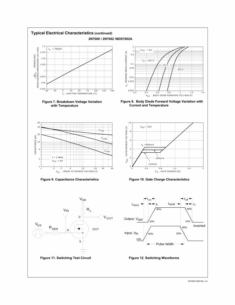
Typical Electrical Characteristics
Figure 1. On-Region Characteristics Figure 2. On-Resistance Variation with GateVoltage and Drain Current
Figure 3. On-Resistance Variationwith Temperature
Figure 4. On-Resistance Variation with DrainCurrent and Temperature
Figure 5. Transfer Characteristics Figure 6. Gate Threshold Variation withTemperature
0 2 4 6 8 100
0.4
0.8
1.2
1.6
2
V , GATE TO SOURCE VOLTAGE (V)
I
, D
RA
IN C
UR
RE
NT
(A
)
V = 10VDS
GS
D
T = -55°CJ 25°C125°C
2N7000 / 2N7002 / NDS7002A
2N7000.SAM Rev. A1
-50 -25 0 25 50 75 100 125 1500.925
0.95
0.975
1
1.025
1.05
1.075
1.1
T , JUNCTION TEM PERATURE (°C)
DR
AIN
-SO
UR
CE
BR
EA
KD
OW
N V
OL
TA
GE
J
BV
, N
OR
MA
LIZ
ED
DS
S
I = 250µAD
0.2 0.4 0.6 0.8 1 1.2 1.40.001
0.005
0.01
0.05
0.1
0.5
1
2
V , BODY DIODE FORWARD VOLTAGE (V)
I
, R
EV
ER
SE
DR
AIN
CU
RR
EN
T (
A) V = 0VGS
T = 125°CJ
SD
S
25°C
-55°C
0 0.4 0.8 1.2 1.6 20
2
4
6
8
10
Q , GATE CHARGE (nC)
V
, G
AT
E-S
OU
RC
E V
OL
TA
GE
(V
)
g
GS
I =500m AD
V = 25VDS
115m A
280m A
1 2 3 5 10 20 30 501
2
5
10
20
40
60
V , DRAIN TO SOURCE VOLTAGE (V)
CA
PA
CIT
AN
CE
(p
F)
DS
C iss
f = 1 MHz
V = 0VGS
C oss
C rss
G
D
S
VDD
R LV
V
IN
OUT
VGSDUT
RGEN
10%
50%
90%
10%
90%
90%
50%Input, Vin
Output, Vout
t on toff
td(off) t ftrt d(on)
Inverted10%
Pulse Width
Figure 7. Breakdown Voltage Variationwith Temperature
Figure 8. Body Diode Forward Voltage Variation withCurrent and Temperature
Figure 9. Capacitance Characteristics Figure 10. Gate Charge Characteristics
Figure 11. Switching Test Circuit Figure 12. Switching Waveforms
Typical Electrical Characteristics (continued)
2N7000 / 2N7002 /NDS7002A

2N7000.SAM Rev. A1
0.0001 0.001 0.01 0.1 1 10 100 3000.001
0.002
0.01
0.05
0.1
0.2
0.5
1
t , TIME (sec)
TR
AN
SIE
NT
TH
ER
MA
L R
ES
ISTA
NC
Er(
t), N
OR
MA
LIZ
ED
EF
FE
CT
IVE
1
Single Pulse
D = 0.5
0.1
0 .05
0 .02
0 .01
0 .2
Duty Cycle, D = t /t1 2
R (t) = r(t) * R
R = (See Datasheet)θJAθJA
θJA
T - T = P * R (t)θJAAJ
P(pk)
t 1 t 2
0.0001 0.001 0.01 0.1 1 10 100 3000.01
0.02
0.05
0.1
0.2
0.5
1
t , TIME (sec)
TR
AN
SIE
NT
TH
ER
MA
L R
ES
ISTA
NC
Er(
t), N
OR
MA
LIZ
ED
EF
FE
CT
IVE
1
Single Pulse
D = 0.5
0.1
0.05
0 .02
0.01
0 .2
Duty Cycle, D = t /t1 2
R (t) = r(t) * R
R = (See Datasheet)θJAθJA
θJA
T - T = P * R (t)θJAAJ
P(pk)
t 1 t 2
1 2 5 10 20 30 60 800.005
0.01
0.05
0.1
0.5
1
2
3
V , DRAIN-SOURCE VOLTAGE (V)
I
, D
RA
IN C
UR
RE
NT
(A
)
DS
D
V = 10V
SINGLE PULSE
T = 25°C
GS
A
RDS(ON) L
imit
100m s
1 m s10m s
DC
1s
100us
10s
Figure 16. TO-92, 2N7000 Transient Thermal Response Curve
Figure 17. SOT-23, 2N7002 / NDS7002A Transient Thermal Response Curve
1 2 5 10 20 30 60 800.005
0.01
0.05
0.1
0.5
1
2
3
V , DRAIN-SOURCE VOLTAGE (V)
I
, D
RA
IN C
UR
RE
NT
(A
)
DS
D
V = 10V
SINGLE PULSE
T = 25°C
GS
A
RDS(ON) L
imit
100m s
1 m s
10m s
DC
1s10s
100us
1 2 5 10 20 30 60 800.005
0.01
0.05
0.1
0.5
1
2
3
V , DRAIN-SOURCE VOLTAGE (V)
I
, D
RA
IN C
UR
RE
NT
(A
)
DS
D V = 10V
SINGLE PULSE
T = 25°C
GS
A
RDS(ON) L
imit
100m s
1 m s
10m s
DC
1s10s
100us
Figure 13. 2N7000 MaximumSafe Operating Area
Figure 14. 2N7002 MaximumSafe Operating Area
Figure 15. NDS7000A MaximumSafe Operating Area
Typical Electrical Characteristics (continued)

TO-92 Tape and Reel Data and Package Dimensions
September 1999, Rev. B
TO-92 PackagingConfiguration: Figure 1.0
AMMO PACK OPTIONSee Fig 3.0 for 2 Ammo
Pack Options
2000 units perEO70 box for
std option
FSCINT Label
530mm x 130mm x
83mmIntermediate box
10,000 units maximumper
intermediate boxfor std option
FSCINT Label
114mm x 102mm x 51mmImmediate Box
Anti-static Bubble Sheets
(TO-92) BULK PACKING INFORMATION
EOLCODE DESCRIPTION LEADCLIP
DIMENSION QUANTITY
J18Z TO-18 OPTION STD NO LEAD CLIP 2.0 K / BOX
J05Z TO-5 OPTION STD NO LEAD CLIP 1.5 K / BOX
NO EOLCODE
TO-92 STANDARDSTRAIGHT NO LEADCLIP 2.0 K / BOX
BULK OPTIONSee Bulk PackingInformation table
375mm x 267mm x 375mmIntermediate Box
FSCINTLabel
CustomizedLabel
333mm x 231mm x 183mmIntermediate Box
FSCINTLabel
CustomizedLabel
TO-92 TNR/AMMO PACKING INFROMATION
Packing Style Quantity EOL code
Reel A 2,000 D26Z
E 2,000 D27Z
Ammo M 2,000 D74Z
P 2,000 D75Z
Unit weight = 0.22 gmReel weight with components = 1.04 kgAmmo weight with components = 1.02 kgMax quantity per intermediate box = 10,000 units
F63TNRLabel
5 Ammo boxes per Intermediate Box
CustomizedLabel
327mm x 158mm x 135mmImmediate Box
LOT: CBVK741B019
NSID: PN2222N
D/C1: D9842 SPEC REV: B2
SPEC:
QTY: 10000
QA REV:
FAIRCHILD SEMICONDUCTOR CORPORATION HTB:B
(FSCINT)
F63TNRLabel
CustomizedLabel
5 Reels perIntermediate Box
TAPE and REEL OPTIONSee Fig 2.0 for various
Reeling Styles
LOT: CBVK741B019
FSID: PN222N
D/C1: D9842 QTY1: SPEC REV:
SPEC:
QTY: 2000
D/C2: QTY2: CPN:N/F: F (F63TNR)3
F63TNR Label sample
FSCINT Label sample
C
5 EO70 boxes per intermediate Box
ustomizedLabel

TO-92 Tape and Reel Data and Package Dimensions, continued
September 1999, Rev. B
TO-92 Reeling StyleConfiguration: Figure 2.0
Style “A”, D26Z, D70Z (s/h)
Machine Option “A” (H)
Style “E”, D27Z, D71Z (s/h)
Machine Option “E” (J)
FIRST WIRE OFF IS EMITTERADHESIVE TAPE IS ON THE TOP SIDEFLAT OF TRANSISTOR IS ON BOTTOM
ORDER STYLED75Z (P)
FIRST WIRE OFF IS COLLECTORADHESIVE TAPE IS ON THE TOP SIDEFLAT OF TRANSISTOR IS ON TOP
ORDER STYLED74Z (M)
TO-92 Radial Ammo PackagingConfiguration: Figure 3.0
FIRST WIRE OFF IS EMITTER (ON PKG. 92)ADHESIVE TAPE IS ON BOTTOM SIDEFLAT OF TRANSISTOR IS ON BOTTOM
FIRST WIRE OFF IS COLLECTOR (ON PKG. 92)ADHESIVE TAPE IS ON BOTTOM SIDEFLAT OF TRANSISTOR IS ON TOP

ITEM DESCRIPTION
Base of Package to Lead Bend
Component Height
Lead Clinch Height
Component Base Height
Component Alignment ( side/side )
Component Alignment ( front/back )
Component Pitch
Feed Hole Pitch
Hole Center to First Lead
Hole Center to Component Center
Lead Spread
Lead Thickness
Cut Lead Length
Taped Lead Length
Taped Lead Thickness
Carrier Tape Thickness
Carrier Tape Width
Hold - down Tape Width
Hold - down Tape position
Feed Hole Position
Sprocket Hole Diameter
Lead Spring Out
SYMBOL
b
Ha
HO
H1
Pd
Hd
P
PO
P1
P2
F1/F2
d
L
L1
t
t1
W
WO
W1
W2
DO
S
DIMENSION
0.098 (max)
0.928 (+/- 0.025)
0.630 (+/- 0.020)
0.748 (+/- 0.020)
0.040 (max)
0.031 (max)
0.500 (+/- 0.020)
0.500 (+/- 0.008)
0.150 (+0.009, -0.010)
0.247 (+/- 0.007)
0.104 (+/- 0 .010)
0.018 (+0.002, -0.003)
0.429 (max)
0.209 (+0.051, -0.052)
0.032 (+/- 0.006)
0.021 (+/- 0.006)
0.708 (+0.020, -0.019)
0.236 (+/- 0.012)
0.035 (max)
0.360 (+/- 0.025)
0.157 (+0.008, -0.007)
0.004 (max)
Note : All dimensions are in inches.
ITEM DESCRIPTION SYSMBOL MINIMUM MAXIMUM
Reel Diameter D1 13.975 14.025
Arbor Hole Diameter (Standard) D2 1.160 1.200
(Small Hole) D2 0.650 0.700
Core Diameter D3 3.100 3.300
Hub Recess Inner Diameter D4 2.700 3.100
Hub Recess Depth W1 0.370 0.570
Flange to Flange Inner Width W2 1.630 1.690
Hub to Hub Center Width W3 2.090
Note: All dimensions are inches
TO-92 Tape and Reel TapingDimension Configuration: Figure 4.0
Ha
H1 HO
PO
P2
P1 F1
DO
P Pd
b
d
L1
LS
WOW2
W
t
t1
Hd
W1
TO-92 ReelConfiguration: Figure 5.0
User Direction of Feed
SEN SITIVE D EVICES
ELECTROSTATIC
D1
D3
Customized Label
W2
W1
W3
F63TNR Label
D4
D2
TO-92 Tape and Reel Data and Package Dimensions, continued
July 1999, Rev. A

TO-92 (FS PKG Code 92, 94, 96)
TO-92 Tape and Reel Data and Package Dimensions
January 2000, Rev. B
1:1Scale 1:1 on letter size paper
Dimensions shown below are in:inches [millimeters]
Part Weight per unit (gram): 0.1977

SOT-23 PackagingConfiguration: Figure 1.0
ComponentsLeader Tape500mm minimum or
125 empty pockets
Trailer Tape300mm minimum or
75 empty pockets
SOT-23 Tape Leader and TrailerConfiguration: Figure 2.0
Cover Tape
Carrier Tape
Note/Comments
Packaging Option
SOT-23 Packaging Information
Standard(no flow code) D87Z
Packaging type
Reel Size
TNR
7" Dia
TNR
13"
Qty per Reel/Tube/Bag 3,000 10,000
Box Dimension (mm) 187x107x183 343x343x64
Max qty per Box 24,000 30,000
Weight per unit (gm) 0.0082 0.0082
Weight per Reel (kg) 0.1175 0.4006
Human readableLabel
Human Readable Label
Human Readable Label sample
343mm x 342mm x 64mmIntermediate box for L87Z Option
187mm x 107mm x 183mmIntermediate Box for Standard Option
SOT-23 Unit Orientation
3P 3P 3P 3P
Human ReadableLabel
Customized Label
EmbossedCarrier Tape
Antistatic Cover Tape
Packaging Description:
SOT-23made from a dissipative (carbon fil led) polycarbonateresin. The cover tape is a multilayer film (Heat ActivatedAdhesive in nature) primarily composed of polyester film,adhesive layer, sealant, and anti-static sprayed agent.These reeled parts in standard option are shipped with3,000 units per 7" or 177cm diameter reel. The reels aredark blue in color and is made of polystyrene plastic (anti-static coated). Other option comes in 10,000 units per 13"or 330cm diameter reel. This and some other options aredescribed in the Packaging Information table.
These full reels are individually labeled and placed insidea standard intermediate made of recyclable corrugatedbrown paper with a Fairchil d logo printing. One pizza boxcontains eight reels maximum. And these intermediateboxes are placed inside a labeled shipping box whichcomes in different sizes depending on the number of partsshipped.
parts are shipped in tape. The carrier tape is
SOT-23 Tape and Reel Data and Package Dimensions
September 1999, Rev. C

Dimensions are in millimeter
Pkg type A0 B0 W D0 D1 E1 E2 F P1 P0 K0 T Wc Tc
SOT-23(8mm)
3.15+/-0.10
2.77+/-0.10
8.0+/-0.3
1.55+/-0.05
1.125+/-0.125
1.75+/-0.10
6.25min
3.50+/-0.05
4.0+/-0.1
4.0+/-0.1
1.30+/-0.10
0.228+/-0.013
5.2+/-0.3
0.06+/-0.02
Dimensions are in inches and millimeters
Tape SizeReel
Option Dim A Dim B Dim C Dim D Dim N Dim W1 Dim W2 Dim W3 (LSL-USL)
8mm 7" Dia 7.00177.8
0.0591.5
512 +0.020/-0.00813 +0.5/-0.2
0.79520.2
2.16555
0.331 +0.059/-0.0008.4 +1.5/0
0.56714.4
0.311 – 0.4297.9 – 10.9
8mm 13" Dia 13.00330
0.0591.5
512 +0.020/-0.00813 +0.5/-0.2
0.79520.2
4.00100
0.331 +0.059/-0.0008.4 +1.5/0
0.56714.4
0.311 – 0.4297.9 – 10.9
See detail AA
Dim Amax
13" Diameter Option
7" Diameter Option
Dim AMax
See detail AA
W3
W2 max Measured at Hub
W1 Measured at Hub
Dim N
Dim Dmin
Dim C
B Min
DETAIL AA
Notes: A0, B0, and K0 dimensions are determined with respect to the EIA/Jedec RS-481rotational and lateral movement requirements (see sketches A, B, and C).
20 deg maximum component rotation
0.5mmmaximum
0.5mmmaximum
Sketch C (Top View)Component lateral movement
Typicalcomponentcavitycenter line
20 deg maximum
Typicalcomponentcenter line
B0
A0
Sketch B (Top View)Component Rotation
Sketch A (Side or Front Sectional View)Component Rotation
User Direction of Feed
SOT-23 Embossed Carrier TapeConfiguration: Figure 3.0
SOT-23 Reel Configuration: Figure 4.0
P1 A0
D1
F W
E1
E2
Tc
Wc
K0
T
B0
D0P0 P2
SOT-23 Tape and Reel Data and Package Dimensions, continued
September 1999, Rev. C

SOT-23 (FS PKG Code 49)
SOT-23 Tape and Reel Data and Package Dimensions, continued
September 1998, Rev. A1
1:1Scale 1:1 on letter size paper
Dimensions shown below are in:inches [millimeters]
Part Weight per unit (gram): 0.0082

TRADEMARKS
ACEx™CoolFET™CROSSVOLT™E2CMOSTM
FACT™FACT Quiet Series™FAST®
FASTr™GTO™HiSeC™
The following are registered and unregistered trademarks Fairchild Semiconductor owns or is authorized to use and isnot intended to be an exhaustive list of all such trademarks.
LIFE SUPPORT POLICY
FAIRCHILD’S PRODUCTS ARE NOT AUTHORIZED FOR USE AS CRITICAL COMPONENTS IN LIFE SUPPORTDEVICES OR SYSTEMS WITHOUT THE EXPRESS WRITTEN APPROVAL OF FAIRCHILD SEMICONDUCTOR CORPORATION.As used herein:1. Life support devices or systems are devices orsystems which, (a) are intended for surgical implant intothe body, or (b) support or sustain life, or (c) whosefailure to perform when properly used in accordancewith instructions for use provided in the labeling, can bereasonably expected to result in significant injury to theuser.
2. A critical component is any component of a lifesupport device or system whose failure to perform canbe reasonably expected to cause the failure of the lifesupport device or system, or to affect its safety oreffectiveness.
PRODUCT STATUS DEFINITIONS
Definition of Terms
Datasheet Identification Product Status Definition
Advance Information
Preliminary
No Identification Needed
Obsolete
This datasheet contains the design specifications forproduct development. Specifications may change inany manner without notice.
This datasheet contains preliminary data, andsupplementary data will be published at a later date.Fairchild Semiconductor reserves the right to makechanges at any time without notice in order to improvedesign.
This datasheet contains final specifications. FairchildSemiconductor reserves the right to make changes atany time without notice in order to improve design.
This datasheet contains specifications on a productthat has been discontinued by Fairchild semiconductor.The datasheet is printed for reference information only.
Formative orIn Design
First Production
Full Production
Not In Production
DISCLAIMER
FAIRCHILD SEMICONDUCTOR RESERVES THE RIGHT TO MAKE CHANGES WITHOUT FURTHERNOTICE TO ANY PRODUCTS HEREIN TO IMPROVE RELIABILITY, FUNCTION OR DESIGN. FAIRCHILDDOES NOT ASSUME ANY LIABILITY ARISING OUT OF THE APPLICATION OR USE OF ANY PRODUCTOR CIRCUIT DESCRIBED HEREIN; NEITHER DOES IT CONVEY ANY LICENSE UNDER ITS PATENTRIGHTS, NOR THE RIGHTS OF OTHERS.
SyncFET™TinyLogic™UHC™VCX™
ISOPLANAR™MICROWIRE™POP™PowerTrenchQFET™QS™Quiet Series™SuperSOT™-3SuperSOT™-6SuperSOT™-8
Rev. D