Embed Size (px)
Citation preview
2nd Generation Intel®
Core™ Processor Family:
Intel® Core™ i7, i5 and i3
Oded Lem pel , Sandy Bridge Design Managem ent
2nd Gen Intel® Core™ Microarchitecture formerly codenamed Sandy Bridge1
Agenda
2
CPU Overview
System Agent, Ring Architecture and System Integration
Core Enhancements and IA Extensions
Integration Challenges
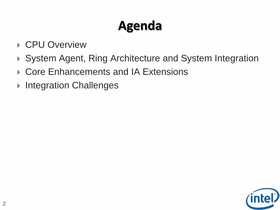
System On Chip Integration
3
CPU and GMCH integrated into a single chip
PCH remains as separate die outside of CPU package
DisplayPort
QPI
QPI
GFX
PCH
Legacy & Debug I / O
Core
Core
LLC
HDvideo
PCIe
Display
PCIe
GMCH
DD
R
DDR3
CPU
2010 Platform
PCI , SATA, USB...
CRT, TVout , HDMI , LVDS
V
DMI
DMI2 Disp Links
ME
2 Disp Links
Analog
x4 Gen1
DisplayPort
PCI , SATA, USB...
CPU (Sandy Bridge)
CRT, TVout , HDMI , LVDS
PCH (Cougar Point )
V
Legacy & Debug I / O
Core
Core
GT
LLC
DMI 2
SADMI 22 Disp Links
ME
HDvideo
2 Disp Links
Analog
DDR3DD
R
x4 Gen2
2011 Platform
PCIe
Display
PCIeDisplay
Port
DisplayPort
CPU and GMCH on the same package in Multi-ChipPackage (MCP) configuration
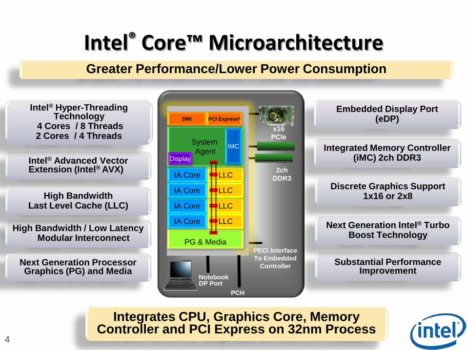
Intel® Core™ Microarchitecture
4
Integrated Memory Controller(iMC) 2ch DDR3Intel ® Advanced Vector
Extension (Intel ® AVX) 2ch DDR3
x16 PCIe
PECI InterfaceTo Embedded
Controller
NotebookDP Port
PG & Media
IA Core LLC
IA Core LLC
IA Core LLC
IA Core LLC
System Agent
Display
DMI PCI Express*
IMC
PCH
Intel ® Hyper -Threading Technology
4 Cores / 8 Threads 2 Cores / 4 Threads
High Bandwidth / Low LatencyModular Interconnect
Substantial Performance Improvement
High BandwidthLast Level Cache (LLC)
Next Generation Processor Graphics (PG) and Media
Next Generation Intel ® Turbo Boost Technology
Discrete Graphics Support 1x16 or 2x8
Embedded Display Port (eDP)
Integrates CPU, Graphics Core, Memory Controller and PCI Express on 32nm Process
Greater Performance/Lower Power Consumption
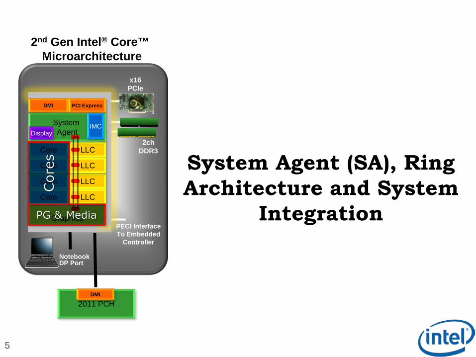
5
System Agent (SA), Ring
Architecture and System
Integration
2ch DDR3
x16 PCIe
PECI InterfaceTo Embedded
Controller
NotebookDP Port
Graphics
Core LLC
Core LLC
Core LLC
Core LLC
System AgentDisplay
DMI PCI Express
IMC
2011 PCHDMI
2nd Gen Intel ® Core™ Microarchitecture
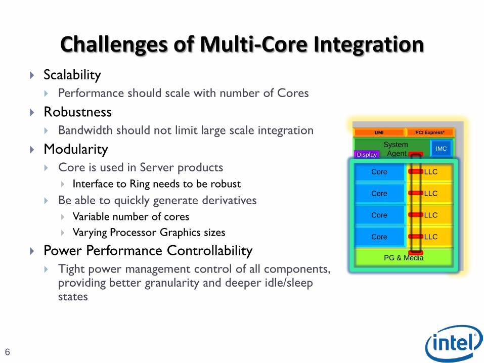
Challenges of Multi-Core Integration
6
Scalability Performance should scale with number of Cores
Robustness Bandwidth should not limit large scale integration
Modularity Core is used in Server products
Interface to Ring needs to be robust
Be able to quickly generate derivatives
Variable number of cores
Varying Processor Graphics sizes
Power Performance Controllability Tight power management control of all components,
providing better granularity and deeper idle/sleep states
PG & Media
Core LLC
Core
Core LLC
Core LLC
System Agent Display
DMI PCI Express*
IMC
LLC
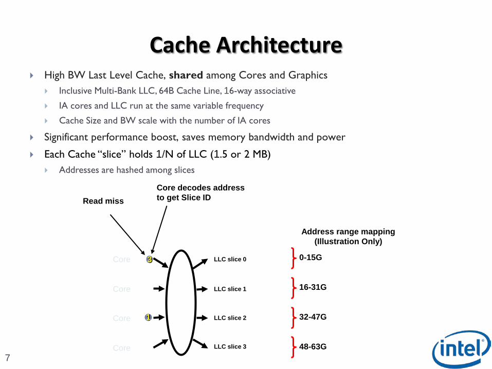
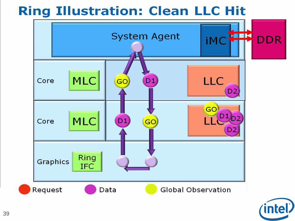
Cache Architecture High BW Last Level Cache, shared among Cores and Graphics
Inclusive Multi-Bank LLC, 64B Cache Line, 16-way associative
IA cores and LLC run at the same variable frequency
Cache Size and BW scale with the number of IA cores
Significant performance boost, saves memory bandwidth and power
Each Cache “slice” holds 1/N of LLC (1.5 or 2 MB)
Addresses are hashed among slices
LLC slice 2
LLC slice 3
Core LLC slice 0
Core LLC slice 1
0-15G
16-31G
32-47G
48-63G
Core
Core
Address range mapping(Illustration Only)
Core decodes addressto get Slice IDRead miss
3
1
7
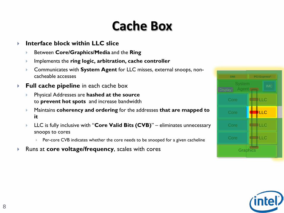
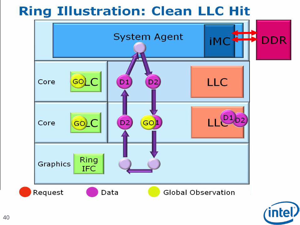
Cache Box
8
Interface block within LLC slice
Between Core/Graphics/Media and the Ring
Implements the ring logic, arbitration, cache controller
Communicates with System Agent for LLC misses, external snoops, non-cacheable accesses
Full cache pipeline in each cache box
Physical Addresses are hashed at the source to prevent hot spots and increase bandwidth
Maintains coherency and ordering for the addresses that are mapped to it
LLC is fully inclusive with “Core Valid Bits (CVB)” – eliminates unnecessary snoops to cores
Per-core CVB indicates whether the core needs to be snooped for a given cacheline
Runs at core voltage/frequency, scales with cores Graphics
Core LLC
Core
Core LLC
Core LLC
System Agent Display
DMI PCI Express*
IMC
LLC
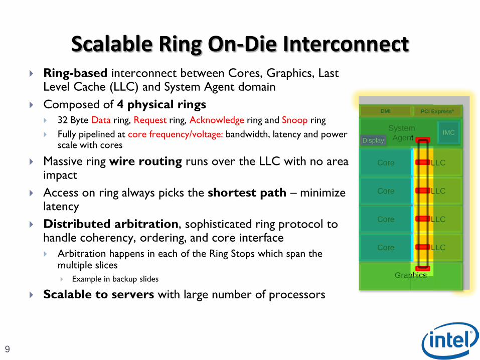
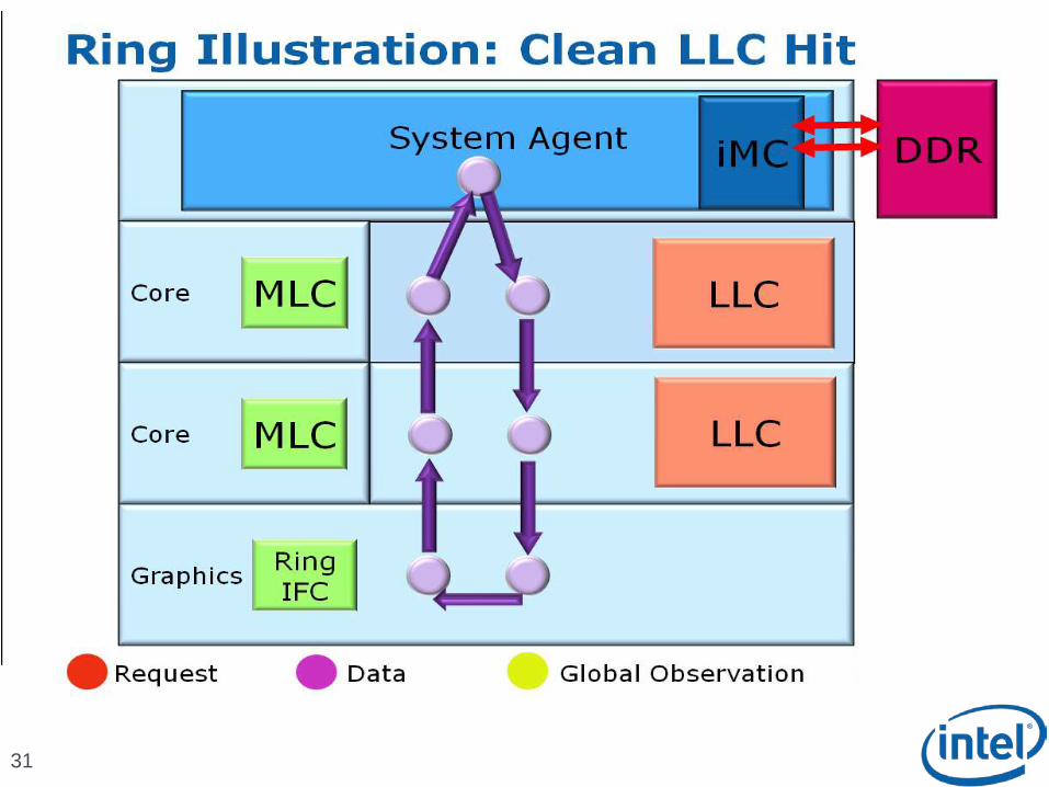
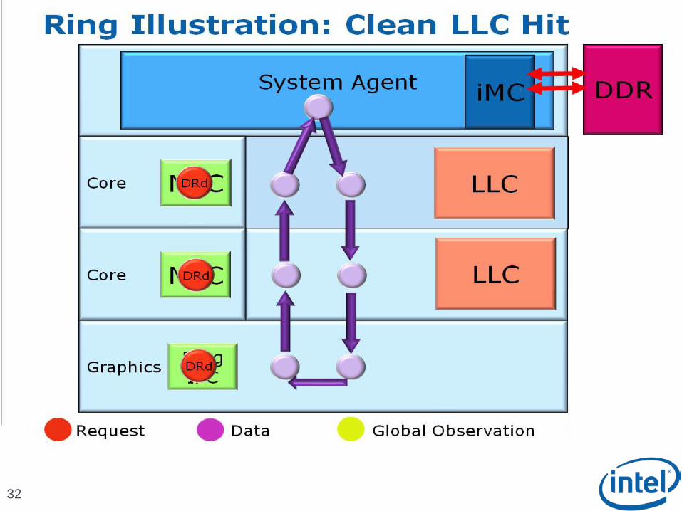
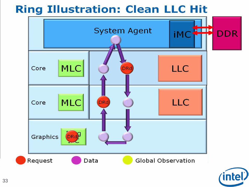
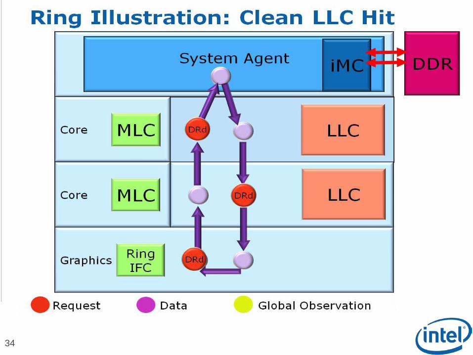
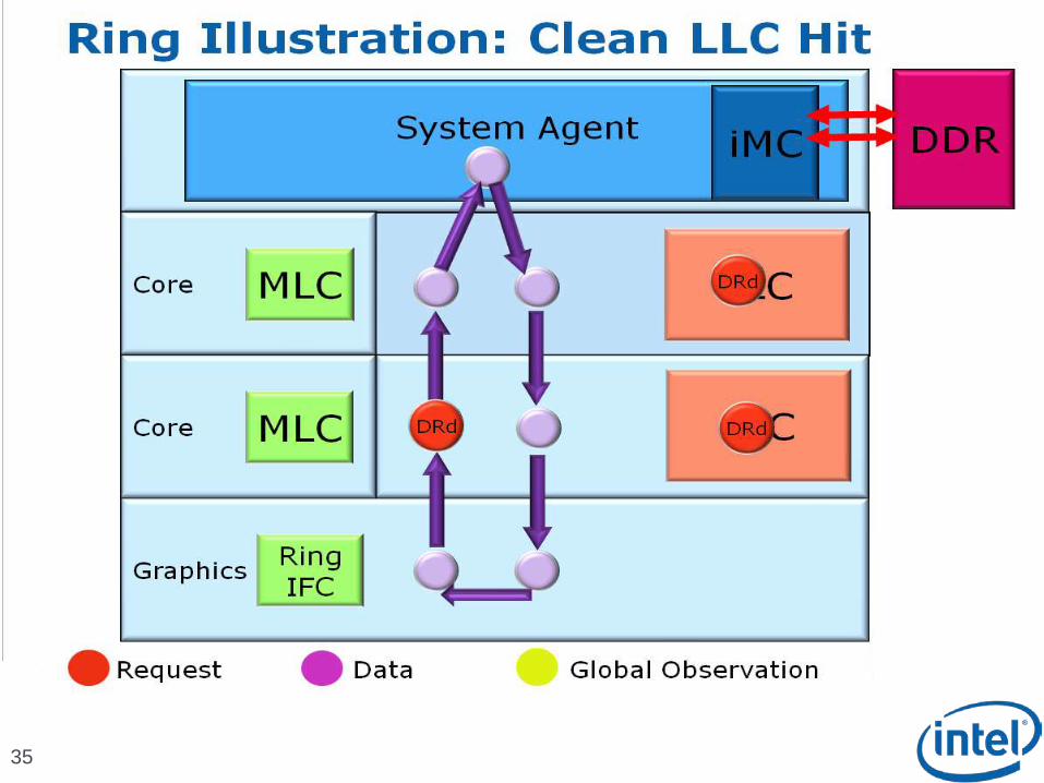
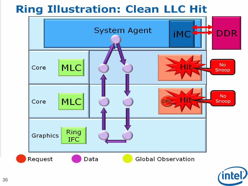
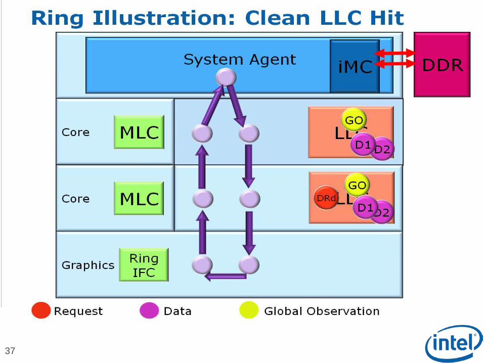
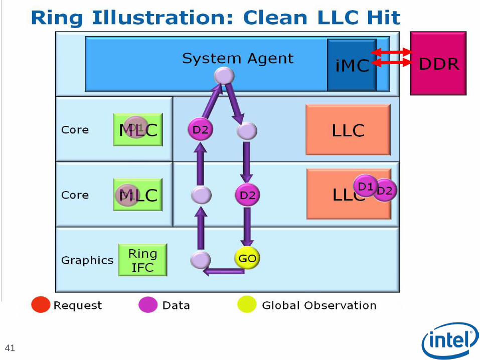
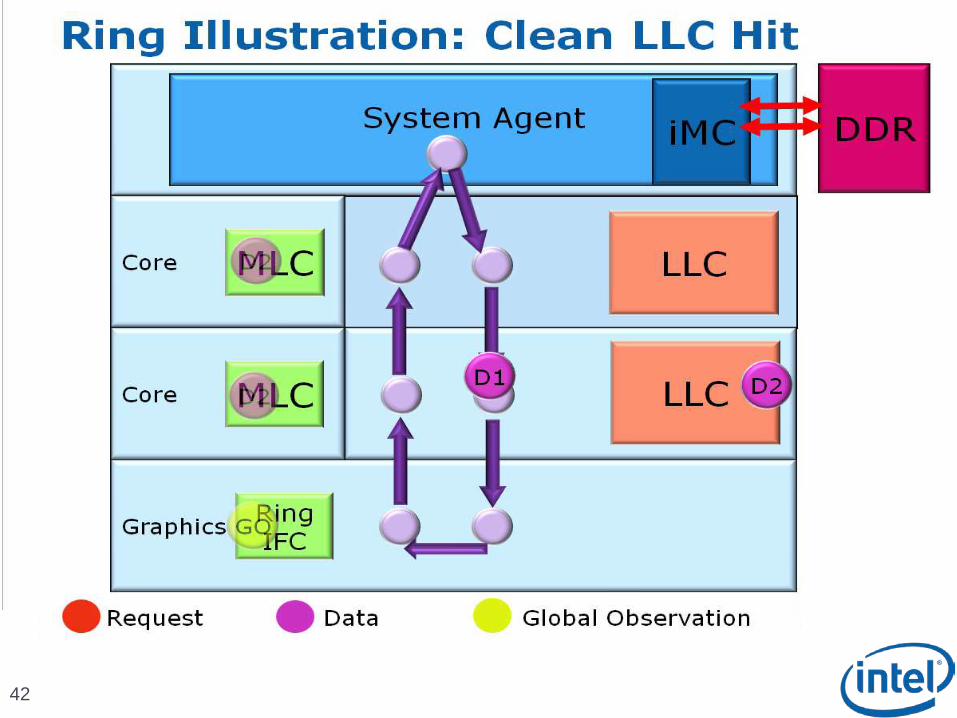
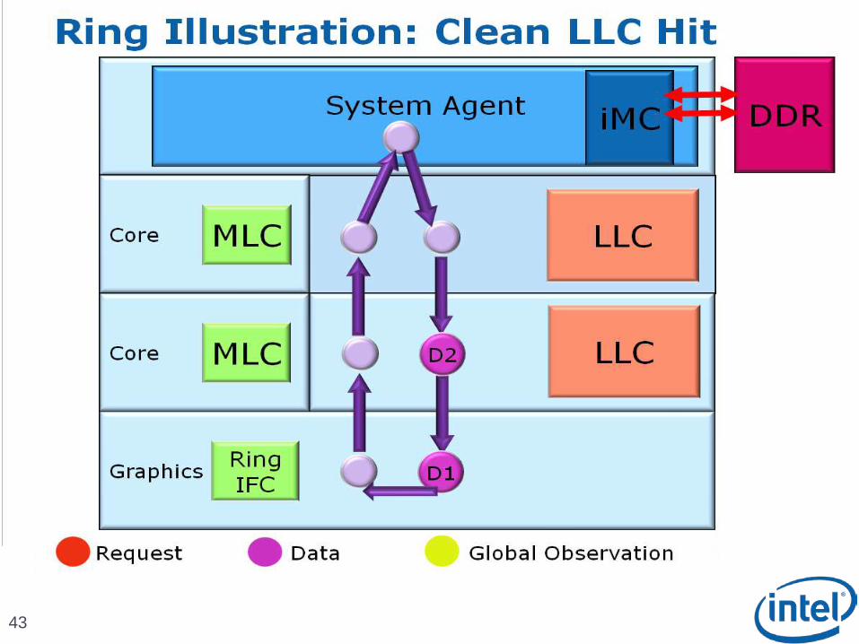
Scalable Ring On-Die Interconnect
9
Ring-based interconnect between Cores, Graphics, Last Level Cache (LLC) and System Agent domain
Composed of 4 physical rings 32 Byte Data ring, Request ring, Acknowledge ring and Snoop ring
Fully pipelined at core frequency/voltage: bandwidth, latency and power scale with cores
Massive ring wire routing runs over the LLC with no area impact
Access on ring always picks the shortest path – minimize latency
Distributed arbitration, sophisticated ring protocol to handle coherency, ordering, and core interface Arbitration happens in each of the Ring Stops which span the
multiple slices
Example in backup slides
Scalable to servers with large number of processors
Graphics
Core LLC
Core
Core LLC
Core LLC
System Agent Display
DMI PCI Express*
IMC
LLC
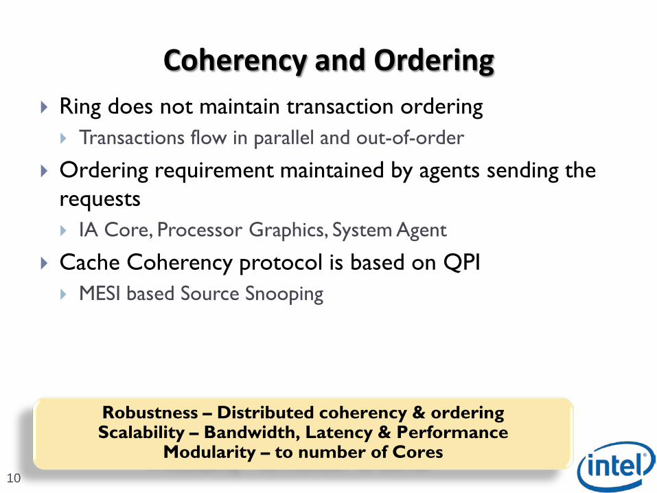
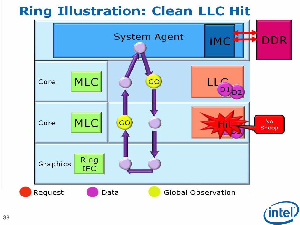
Coherency and Ordering
10
Ring does not maintain transaction ordering
Transactions flow in parallel and out-of-order
Ordering requirement maintained by agents sending the requests
IA Core, Processor Graphics, System Agent
Cache Coherency protocol is based on QPI
MESI based Source Snooping
Robustness – Distributed coherency & ordering Scalability – Bandwidth, Latency & Performance
Modularity – to number of Cores
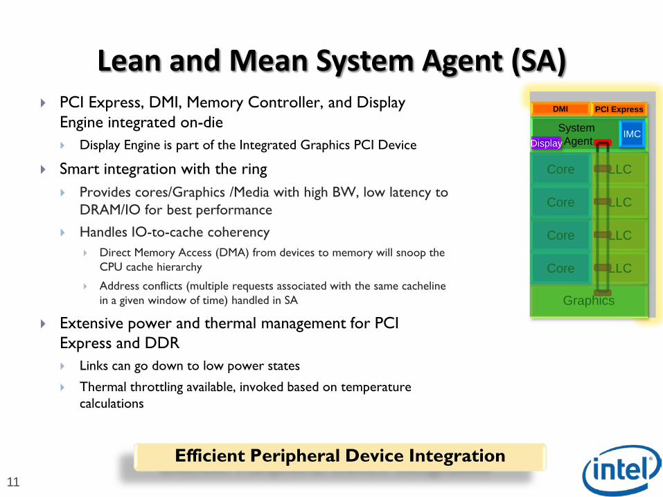
Lean and Mean System Agent (SA)
11
PCI Express, DMI, Memory Controller, and Display Engine integrated on-die
Display Engine is part of the Integrated Graphics PCI Device
Smart integration with the ring
Provides cores/Graphics /Media with high BW, low latency to DRAM/IO for best performance
Handles IO-to-cache coherency
Direct Memory Access (DMA) from devices to memory will snoop the CPU cache hierarchy
Address conflicts (multiple requests associated with the same cachelinein a given window of time) handled in SA
Extensive power and thermal management for PCI Express and DDR
Links can go down to low power states
Thermal throttling available, invoked based on temperature calculations
Efficient Peripheral Device Integration
Graphics
Core LLC
Core
Core LLC
Core LLC
System Agent Display
DMI PCI Express
IMC
LLC
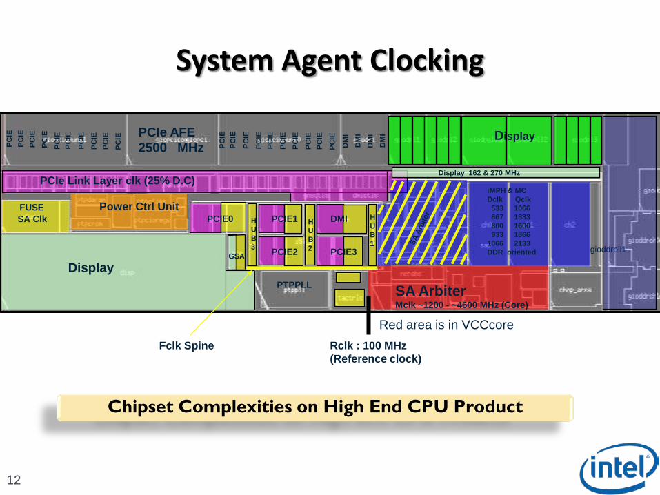
System Agent Clocking
12
Chipset Complexities on High End CPU Product
Display
PC
IE
PC
IE
PC
IE
PC
IE
PC
IEP
CIE
PC
IE
PC
IE
PC
IE
PC
IE
PC
IEP
CIE
PC
IE
PC
IE
PC
IE
PC
IE
PC
IE
PC
IE
PC
IE
PC
IE
DM
I
DM
I
DM
I
DM
IPCIe AFE2500 MHz
Display
PCIe Link Layer clk (25% D.C)
DMIPCIE1
PCIE2
PCIE0
PCIE3
HUB2
HUB3
iMPH & MCDclk Qclk533 1066667 1333 800 1600933 1866
1066 2133 DDR oriented
FUSESA Clk
GSA
Power Ctrl Unit
Rclk : 100 MHz(Reference clock )
Fclk Spine
SA ArbiterMclk ~1200 - ~4600 MHz (Core)
Red area is in VCCcore
gioddrpll1
HUB1
Display 162 & 270 MHz
PTPPLL
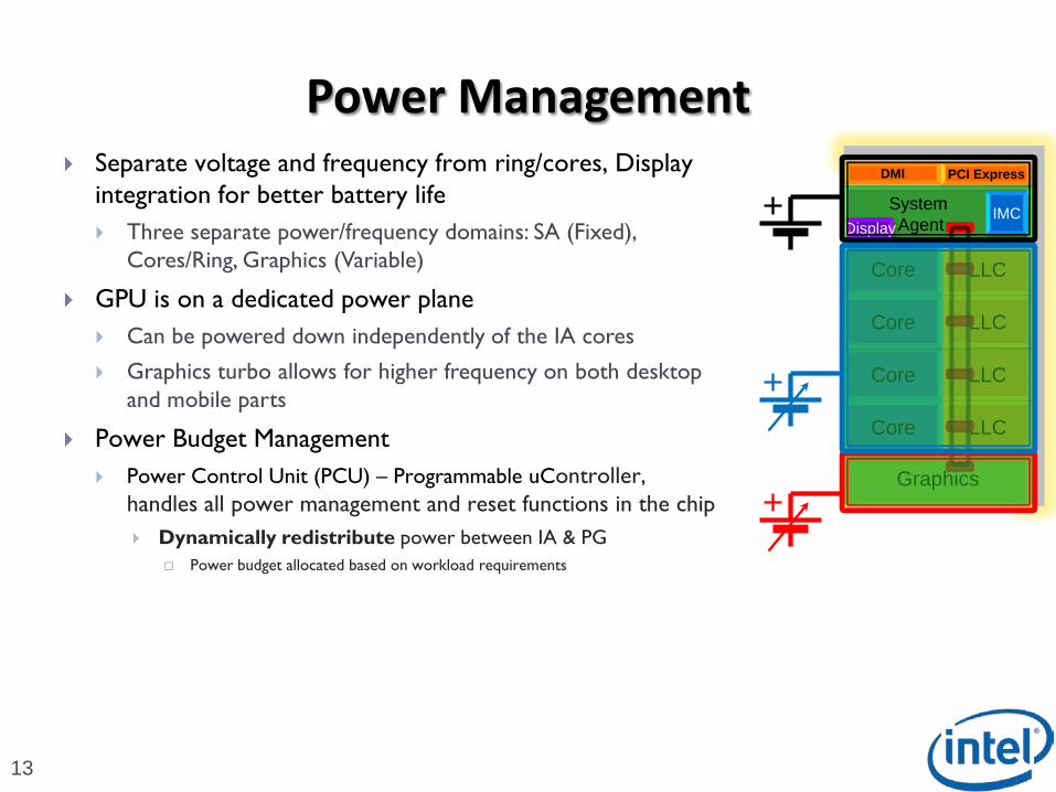
Power Management
13
Separate voltage and frequency from ring/cores, Display integration for better battery life
Three separate power/frequency domains: SA (Fixed), Cores/Ring, Graphics (Variable)
GPU is on a dedicated power plane
Can be powered down independently of the IA cores
Graphics turbo allows for higher frequency on both desktop and mobile parts
Power Budget Management
Power Control Unit (PCU) – Programmable uController, handles all power management and reset functions in the chip
Dynamically redistribute power between IA & PG
Power budget allocated based on workload requirements
Graphics
Core LLC
Core
Core LLC
Core LLC
System Agent Display
DMI PCI Express
IMC
LLC
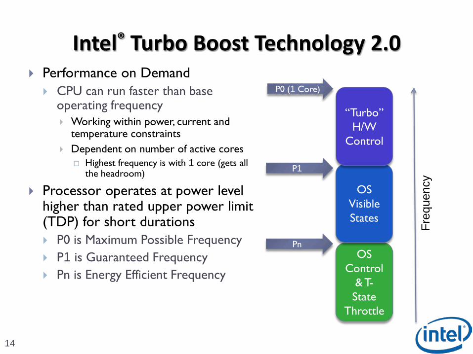
Intel® Turbo Boost Technology 2.0
14
Performance on Demand
CPU can run faster than base operating frequency Working within power, current and
temperature constraints
Dependent on number of active cores Highest frequency is with 1 core (gets all
the headroom)
Processor operates at power level higher than rated upper power limit (TDP) for short durations
P0 is Maximum Possible Frequency
P1 is Guaranteed Frequency
Pn is Energy Efficient Frequency
OS Control
& T-State
Throttle
OS Visible States
“Turbo” H/W
Control
Fre
quen
cy
Pn
P1
P0 (1 Core)
15
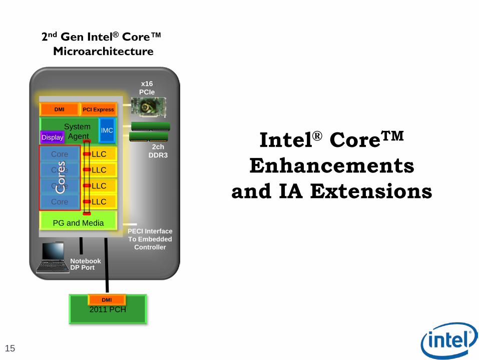
Intel® CoreTM
Enhancements
and IA Extensions
2ch DDR3
x16 PCIe
PECI InterfaceTo Embedded
Controller
NotebookDP Port
PG and Media
Core LLC
Core LLC
Core LLC
Core LLC
System AgentDisplay
DMI PCI Express
IMC
2011 PCHDMI
2nd Gen Intel® Core™ Microarchitecture
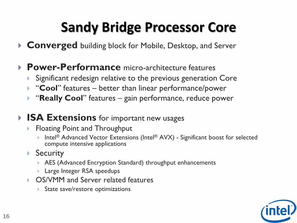
Sandy Bridge Processor Core
16
Converged building block for Mobile, Desktop, and Server
Power-Performance micro-architecture features
Significant redesign relative to the previous generation Core “Cool” features – better than linear performance/power “Really Cool” features – gain performance, reduce power
ISA Extensions for important new usages Floating Point and Throughput
Intel® Advanced Vector Extensions (Intel® AVX) - Significant boost for selected compute intensive applications
Security AES (Advanced Encryption Standard) throughput enhancements
Large Integer RSA speedups
OS/VMM and Server related features State save/restore optimizations
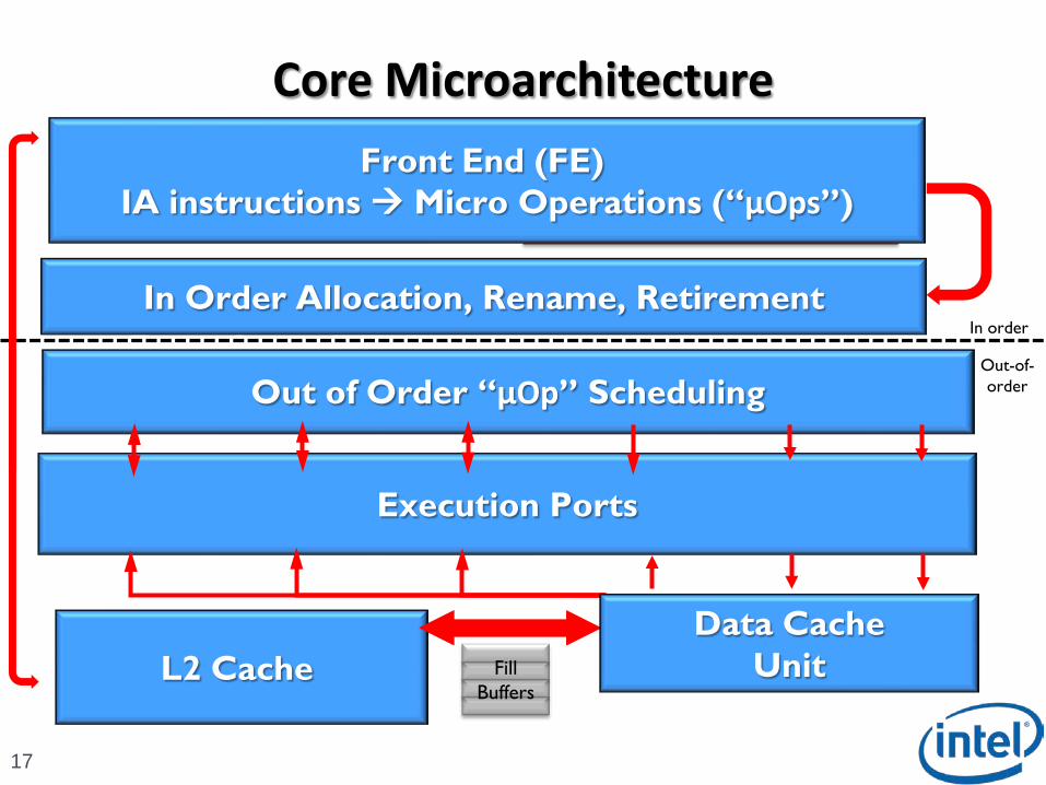
Core Microarchitecture
17
ALU, SI MUL,
DI V, FP MUL
ALU, SI ALU,
FP ADD
ALU, Branch,
FP Shuffle
Load Load
Store Address Store Address
Store
DataExecution Ports
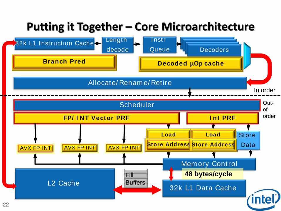
32k L1 I nst ruct ion Cache
Scheduler
Port 0 Port 1 Port 5 Port 2 Port 3 Port 4
32k L1 Data Cache 48 bytes/ cycle
Allocate/ Renam e/ Ret ireZeroing I diomsLoad Buffers
Store Buffers
ReorderBuffers
L2 Cache Fill Buffers
Pre decodeI nst ruct ion
QueueDecoders
1.5k uOP cache
DecodersDecodersDecoders
Branch Pred
In order
Out-of-order
Front End (FE) IA instructions Micro Operations (“μOps”)
In Order Allocation, Rename, Retirement
Out of Order “μOp” Scheduling
Data CacheUnit
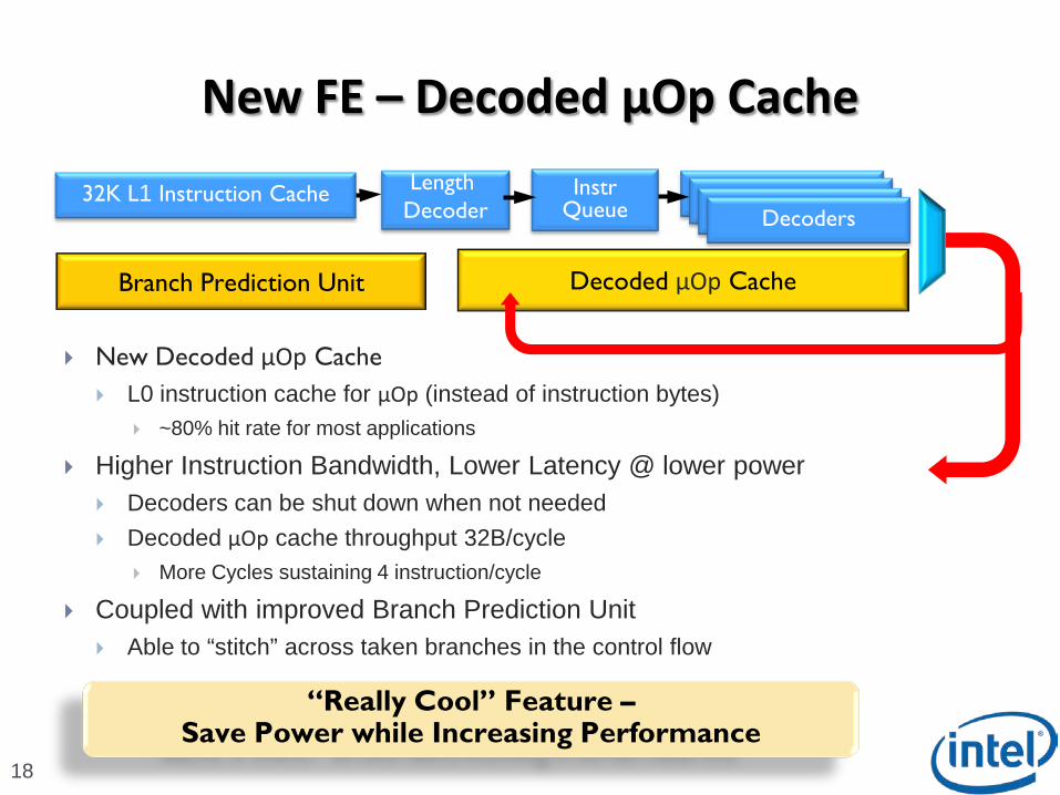
New FE – Decoded μOp Cache
18
New Decoded μOp Cache
L0 instruction cache for μOp (instead of instruction bytes) ~80% hit rate for most applications
Higher Instruction Bandwidth, Lower Latency @ lower power Decoders can be shut down when not needed
Decoded μOp cache throughput 32B/cycle More Cycles sustaining 4 instruction/cycle
Coupled with improved Branch Prediction Unit Able to “stitch” across taken branches in the control flow
Decoded μOp CacheBranch Prediction Unit
32K L1 Instruction CacheLength
DecoderInstr
QueueDecodersDecodersDecodersDecoders
“Really Cool” Feature –Save Power while Increasing Performance
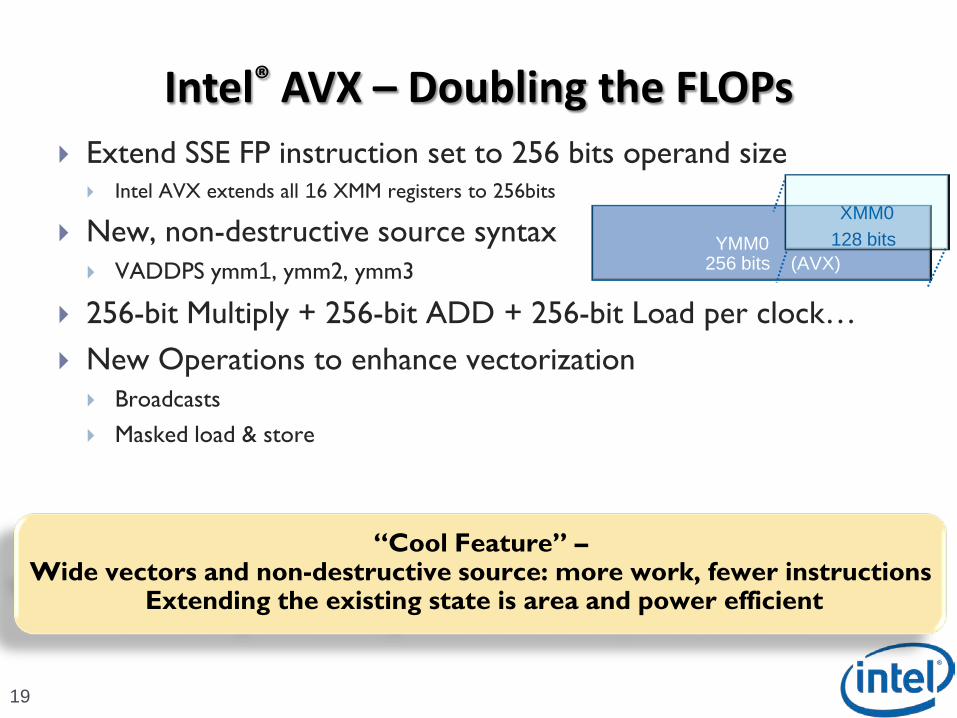
Intel® AVX – Doubling the FLOPs
19
Extend SSE FP instruction set to 256 bits operand size Intel AVX extends all 16 XMM registers to 256bits
New, non-destructive source syntax VADDPS ymm1, ymm2, ymm3
256-bit Multiply + 256-bit ADD + 256-bit Load per clock…
New Operations to enhance vectorization Broadcasts
Masked load & store
YMM0
XMM0128 bits
256 bits (AVX)
“Cool Feature” –Wide vectors and non-destructive source: more work, fewer instructions
Extending the existing state is area and power efficient
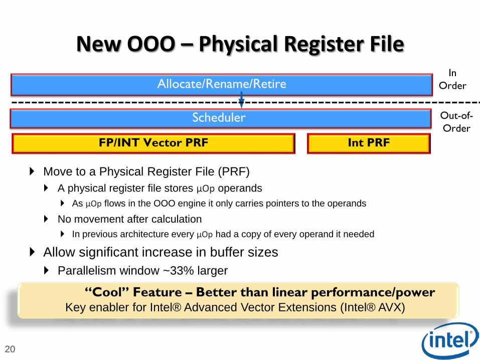
New OOO – Physical Register File
20
Move to a Physical Register File (PRF) A physical register file stores μOp operands
As μOp flows in the OOO engine it only carries pointers to the operands
No movement after calculation In previous architecture every μOp had a copy of every operand it needed
Allow significant increase in buffer sizes Parallelism window ~33% larger
Scheduler
Allocate/Rename/RetireIn
Order
Out-of-Order
FP/INT Vector PRF
“Cool” Feature – Better than linear performance/powerKey enabler for Intel® Advanced Vector Extensions (Intel® AVX)
Int PRF
21
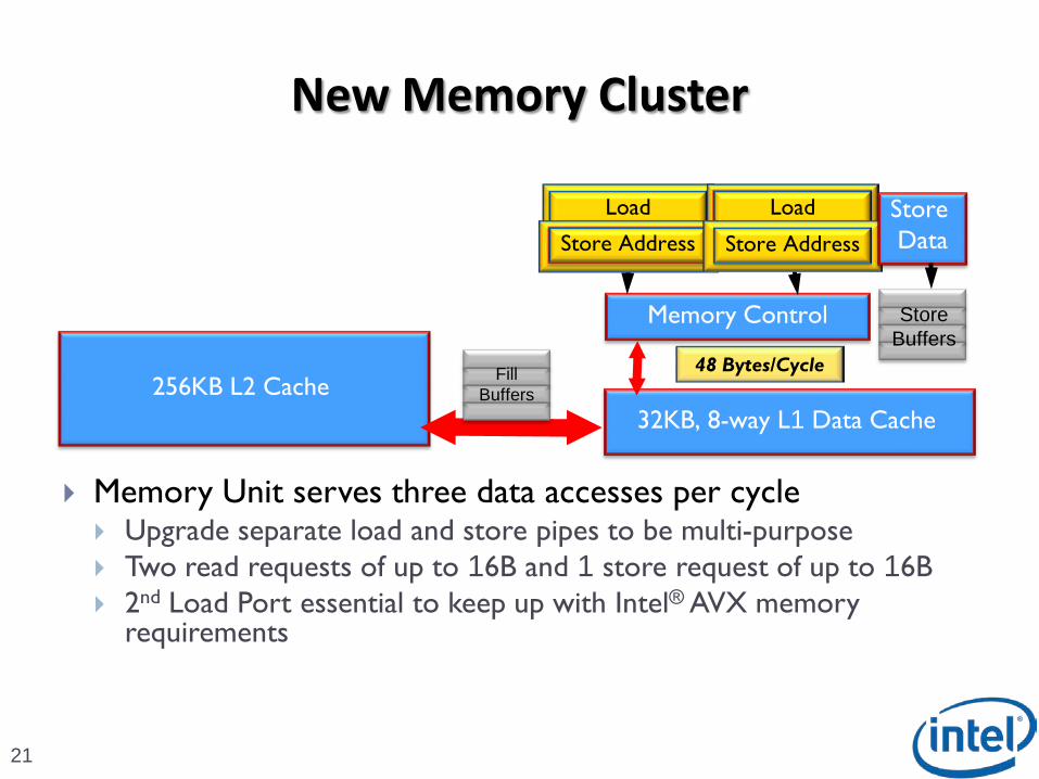
Memory Unit serves three data accesses per cycle Upgrade separate load and store pipes to be multi-purpose Two read requests of up to 16B and 1 store request of up to 16B 2nd Load Port essential to keep up with Intel® AVX memory
requirements
Memory Control
32KB, 8-way L1 Data Cache
48 Bytes/Cycle
Load Load
Store Address Store Address
Store Data
256KB L2 Cache Fill
Buffers
Store Buffers
New Memory Cluster
Putting it Together – Core Microarchitecture
22
32k L1 I nst ruct ion Cache
Scheduler
Mem ory Cont rol
32k L1 Data Cache
48 bytes/cycle
Allocate/ Renam e/ Ret ire
Load Load
Store Address Store Address
Store
Data
L2 Cache Fill Buffers
Length
decode
I nst r
QueueDecoders
Decoded μOp cache
DecodersDecodersDecoders
Branch Pred
In order
Out-of-order
AVX FP I NT
FP/ I NT Vector PRF I nt PRF
AVX FP I NTAVX FP I NT
23
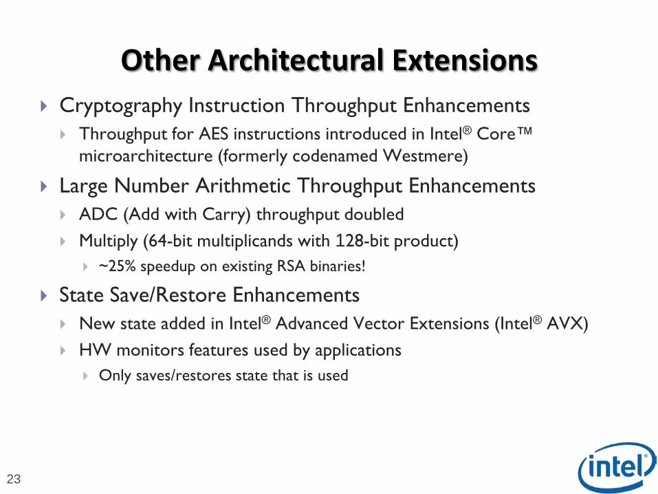
Cryptography Instruction Throughput Enhancements
Throughput for AES instructions introduced in Intel® Core™ microarchitecture (formerly codenamed Westmere)
Large Number Arithmetic Throughput Enhancements
ADC (Add with Carry) throughput doubled
Multiply (64-bit multiplicands with 128-bit product)
~25% speedup on existing RSA binaries!
State Save/Restore Enhancements
New state added in Intel® Advanced Vector Extensions (Intel® AVX)
HW monitors features used by applications
Only saves/restores state that is used
Other Architectural Extensions
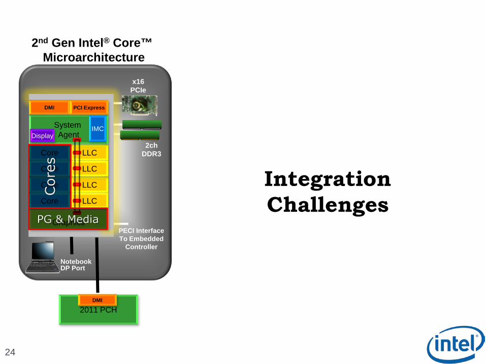
24
Integration
Challenges
2ch DDR3
x16 PCIe
PECI InterfaceTo Embedded
Controller
NotebookDP Port
Graphics
Core LLC
Core LLC
Core LLC
Core LLC
System AgentDisplay
DMI PCI Express
IMC
2011 PCHDMI
2nd Gen Intel ® Core™ Microarchitecture
25
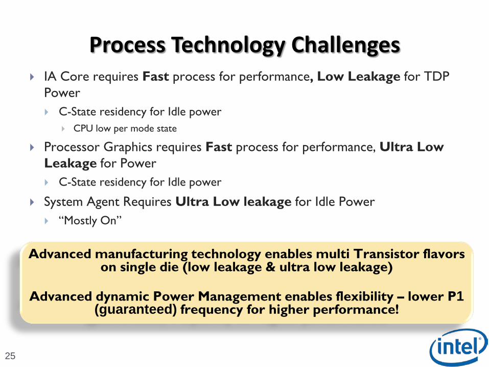
IA Core requires Fast process for performance, Low Leakage for TDP Power
C-State residency for Idle power
CPU low per mode state
Processor Graphics requires Fast process for performance, Ultra Low Leakage for Power
C-State residency for Idle power
System Agent Requires Ultra Low leakage for Idle Power
“Mostly On”
Advanced manufacturing technology enables multi Transistor flavors on single die (low leakage & ultra low leakage)
Advanced dynamic Power Management enables flexibility – lower P1 (guaranteed) frequency for higher performance!
Process Technology Challenges
Process Technology Challenges
26
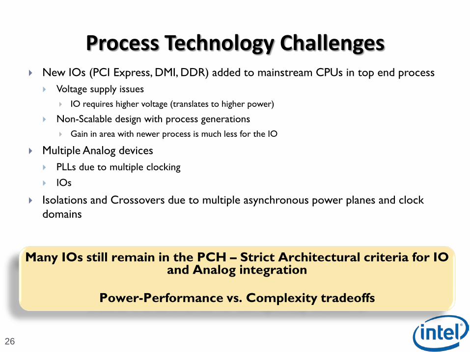
New IOs (PCI Express, DMI, DDR) added to mainstream CPUs in top end process
Voltage supply issues
IO requires higher voltage (translates to higher power)
Non-Scalable design with process generations
Gain in area with newer process is much less for the IO
Multiple Analog devices
PLLs due to multiple clocking
IOs
Isolations and Crossovers due to multiple asynchronous power planes and clock domains
Many IOs still remain in the PCH – Strict Architectural criteria for IO and Analog integration
Power-Performance vs. Complexity tradeoffs
27
Summary32nm Next Generation Core®
Microarchitecture
Processor Graphics
System Agent, Ring Architecture and Other Innovations
Intel® AVX
Performance and Power Efficiency

28
Q&A
Glossary
29
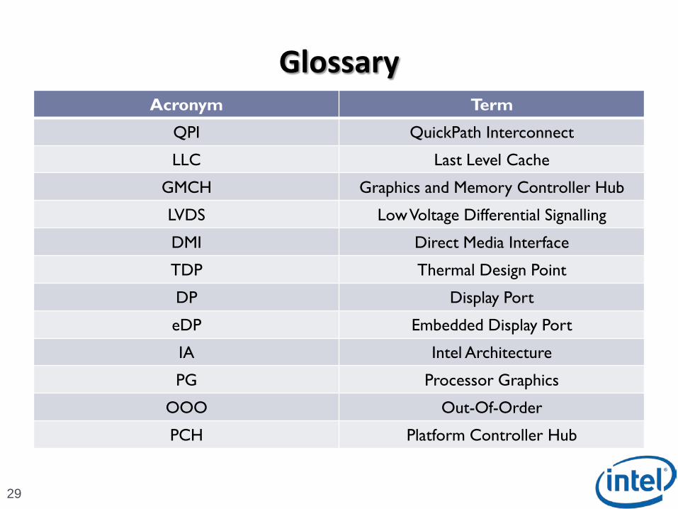
Acronym Term
QPI QuickPath Interconnect
LLC Last Level Cache
GMCH Graphics and Memory Controller Hub
LVDS Low Voltage Differential Signalling
DMI Direct Media Interface
TDP Thermal Design Point
DP Display Port
eDP Embedded Display Port
IA Intel Architecture
PG Processor Graphics
OOO Out-Of-Order
PCH Platform Controller Hub
Glossary (cont)
30
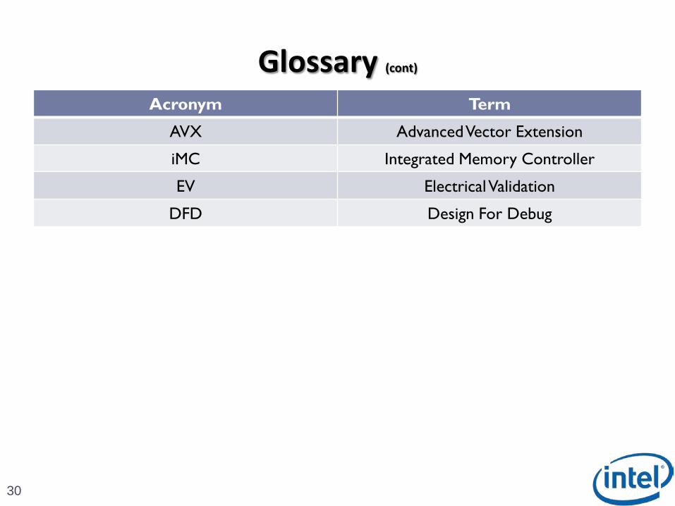
Acronym Term
AVX Advanced Vector Extension
iMC Integrated Memory Controller
EV Electrical Validation
DFD Design For Debug
31
32
33
34
35
36
37
38
39
40
41
42
43

44

45
Validation Challenges
46
Full-Chip
Model size
Turnaround time
Stimuli controllability
Knowledge and Expertise
The product is much more multidisciplinary
Stronger Architectural and Logic orientation
Agility to late changes
Post Silicon Validation and Debug
47
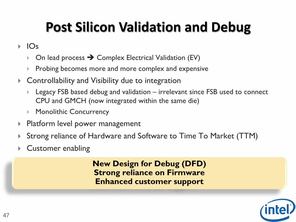
IOs
On lead process Complex Electrical Validation (EV)
Probing becomes more and more complex and expensive
Controllability and Visibility due to integration
Legacy FSB based debug and validation – irrelevant since FSB used to connect CPU and GMCH (now integrated within the same die)
Monolithic Concurrency
Platform level power management
Strong reliance of Hardware and Software to Time To Market (TTM)
Customer enabling
New Design for Debug (DFD)Strong reliance on FirmwareEnhanced customer support
Post Silicon Validation and Debug
48
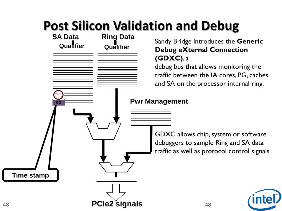
Ring Data
48
Pwr Management
SA DataQualifier Qualifier
PCIe2 signals
0 2
Time stamp
Sandy Bridge introduces the Generic Debug eXternal Connection (GDXC), adebug bus that allows monitoring the traffic between the IA cores, PG, caches and SA on the processor internal ring.
GDXC allows chip, system or software debuggers to sample Ring and SA data traffic as well as protocol control signals