Embed Size (px)
Citation preview
3-3
978-1-4799-5288-5/14/$31.00 c⃝ 2014 IEEE 41
Verilog-A Compact Model for Oxide-based Resistive
Random Access Memory(RRAM)
Zizhen Jiang1, Shimeng Yu2, Yi Wu3, Jesse H. Engel1, Ximeng Guan4, H. –S. Philip Wong1
1Center for Integrated Systems and Department of Electrical Engineering, Stanford University, Stanford, CA 94305, USA, 2School of Computing, Informatics and Decision Systems Engineering, Arizona State University, Tempe, AZ 85281, USA,
3Oracle America, Inc, CA USA, 4IBM Research, NY, USAEmail: [email protected], [email protected], [email protected]
Abstract—We demonstrate a dynamic Verilog-A
RRAM compact model capable of simulating real-time
DC cycling and pulsed operation device behavior,
including random variability that is inherent to RRAM.
This paper illustrates the physics and capabilities of the
model. The model is verified using different sets of
experimental data. The DC/Pulse parameter fitting
methodology are illustrated.
Keywords—RRAM; Compact model; variations;
Verilog-A.
I. INTRODUCTION
Metal-oxide based bipolar resistive random access memory (RRAM) is a promising candidate for the future of nonvolatile memory technology [1]. To fulfill the increasing need for high level simulation of emerging memories, several analytical compact analytical models have been developed to describe resistive switching behavior [2][3][4][5][6]. However, these models fail to consider the stochastic aspect of filament switching or were not implemented effectively for circuit simulation. In this paper, we demonstrate a dynamic RRAM compact model using the circuit-compatible Verilog-A language. This RRAM compact model takes into account filament growth fluctuations and variations. The model is verified using both DC switching data and pulse data. Pulse data fitting is found to be more efficient, more representative of the practical usage scenario, and follows more closely the physics of the filament growth.
II. VERILOG-A RRAM COMPACT MODEL
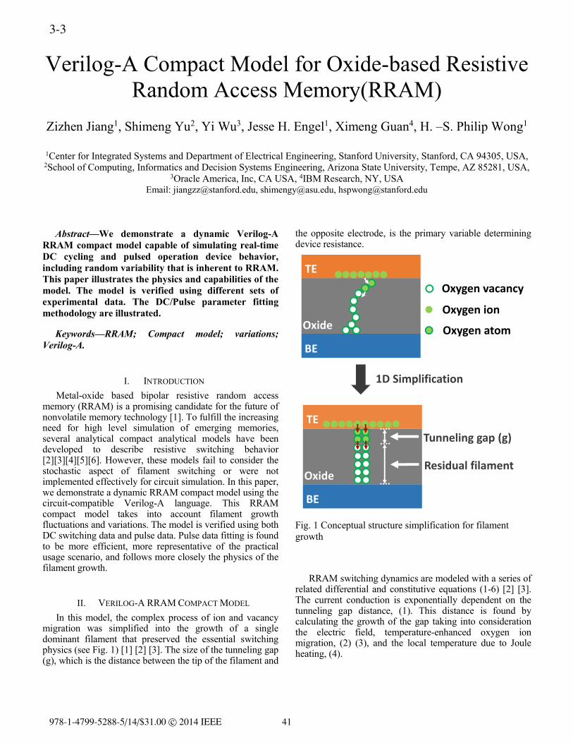
In this model, the complex process of ion and vacancy migration was simplified into the growth of a single dominant filament that preserved the essential switching physics (see Fig. 1) [1] [2] [3]. The size of the tunneling gap (g), which is the distance between the tip of the filament and
the opposite electrode, is the primary variable determining device resistance.
Fig. 1 Conceptual structure simplification for filament
growth
RRAM switching dynamics are modeled with a series of
related differential and constitutive equations (1-6) [2] [3]. The current conduction is exponentially dependent on the tunneling gap distance, (1). This distance is found by calculating the growth of the gap taking into consideration the electric field, temperature-enhanced oxygen ion migration, (2) (3), and the local temperature due to Joule heating, (4).
1D Simplification
Oxygen vacancy
Oxygen ion
Oxygen atom
TE
BE
Oxide
Tunneling gap (g)
TE
BE
OxideResidual filament
42
𝐼 = 𝐼0 × exp(−𝑔
𝑔0) × sinh(
𝑉
𝑉0)
dg
dt= −𝑣0 × exp(−
𝐸𝑎
𝑘𝑇) × sinh (𝑟 ×
𝑎0
𝑡𝑜𝑥×
𝑞𝑉
𝑘𝑇)
𝛾 = 𝛾0 − 𝛽 ∙ 𝑔3
𝑇 = 𝑇0 + 𝑉 × 𝐼 × 𝑅𝑡ℎ
where V is the applied voltage across the cell, I is the current through the cell, g is the average tunneling gap distance, Ea is the activation energy, a0 is the atomic spacing, tox is the oxide thickness, q is the elementary charge, k is the Boltzmann constant, T0 is the room temperature, Rth is the equivalent thermal resistance, and I0, g0, V0, ν0, β, γ0, are fitting parameters.
The use of equivalent thermal resistance in (4) allows us
to avoid using the differential equation for the Joule heating temperature used previously in the literature [3]. Currently, differential equations may require implementations outside the Verilog-A program, thereby rendering the Verilog-A program ineffective.
Stochastic and temperature-dependent filament migration (δg) is also included in the model (5) (6):
𝛿𝑔(𝑇) =𝛿𝑔0
{1+𝑒𝑥𝑝[(𝑇𝑐𝑟𝑖𝑡−𝑇)
𝑇𝑠𝑚𝑡ℎ]}
𝑔|𝑡+∆𝑡 = ∫(𝑑𝑔
𝑑𝑡+𝛿𝑔 × 𝜒(𝑡)) 𝑑𝑡
where Tcrit (400–450 K) is a threshold temperature above which significant random variation of the gap size occurs, χ(t) is a zero-mean Gaussian noise sequence with a root mean square of unity, and δ0 and Tsmth (smoothing factor) are fitting coefficients matching the resistance distribution curves to experimental results. The total gap growth as a function of time is shown in (6).
III. MODEL VERIFICATION
Multiple devices are used to verify the model. Here, we illustrate two fitting processes: DC switching fitting and pulse fitting. After setting the fitting parameters in the Verilog-A program to the extracted values, we can apply the program in circuit-level simulation.
A. DC Switching Fitting
The procedure of DC switching fitting is as follows. First, deterministic switching behavior is fitted.
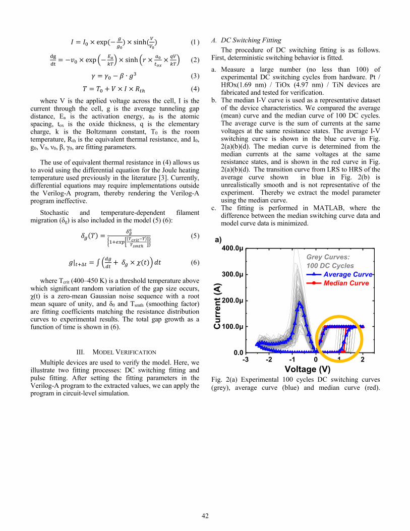
a. Measure a large number (no less than 100) of experimental DC switching cycles from hardware. Pt / HfOx(1.69 nm) / TiOx (4.97 nm) / TiN devices are fabricated and tested for verification.
b. The median I-V curve is used as a representative dataset of the device characteristics. We compared the average (mean) curve and the median curve of 100 DC cycles. The average curve is the sum of currents at the same voltages at the same resistance states. The average I-V switching curve is shown in the blue curve in Fig. 2(a)(b)(d). The median curve is determined from the median currents at the same voltages at the same resistance states, and is shown in the red curve in Fig. 2(a)(b)(d). The transition curve from LRS to HRS of the average curve shown in blue in Fig. 2(b) is unrealistically smooth and is not representative of the experiment. Thereby we extract the model parameter using the median curve.
c. The fitting is performed in MATLAB, where the difference between the median switching curve data and model curve data is minimized.
Fig. 2(a) Experimental 100 cycles DC switching curves
(grey), average curve (blue) and median curve (red).
-3 -2 -1 0 1 20.0
100.0μ
200.0μ
300.0μ
400.0μ
Cu
rre
nt
(A)
Voltage (V)
Grey Curves:
100 DC Cycles
Average Curve
Median Curve
a)
43
Fig. 2(b) Zoom-in figure for fig. 2(a) SET part.
Fig. 2(c) Gaussian distribution of the SET voltages.
Fig. 2(d) Log scale DC switching curve, same data as in
Fig. 2(a).
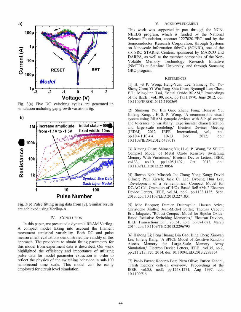
Variations are added later by tuning the fitting parameters in (5) to match the experimental data. Random DC switching cycles generated by simulation are given in Fig. 3(a).
B. Pulse Fitting
Data for pulse fitting is acquired by applying different pulse amplitudes (Fig. 3(b)) and different pulse widths with various initial resistance values [2]. Pulse fitting is important and necessary for the following reasons,
(1) In a memory system, memory cells are written by a write-and-verify scheme using a series of pulses [7]. Tracking memory system performance is especially important for determining cell disturbance, enabling storage failure recovery, etc.
(2) Filament evolution generally happens on a nanosecond timescale. Accessing RRAM may take less than 10 ns, which requires the modeling of RRAM device behavior on the nanosecond time scale.
(3) Considering the nanosecond time scales of filament formation, simulating the DC switching I-V curve requires ~109 calculation per sweep with uniform time steps. For larger time steps, the simulations inaccurately reflect the dynamics of the filament. As observed from experimental data in Fig. 3 (b), resistance tends to saturate after a certain elapsed time. Thus DC fitting may not capture the switching dynamics in the sub-100 nsec regime.
1.0 1.5 2.00.0
50.0μ
100.0μ
150.0μ
Cu
rre
nt
(A)
Voltage (V)
b)
0.9 1.0 1.1 1.2 1.3 1.4 1.5 1.60
5
10
15
20
25
30
Co
un
ts (
#)
SET Voltage (V)
V
V
c)
-3 -2 -1 0 1 210p
100p
1n
10n
100n
1μ
10μ
100μ
1m
Cu
rre
nt
(A)
Voltage (V)
Average Curve
Median Curve
Grey Curves:
100 DC Cycles
d)
44
Fig. 3(a) Five DC switching cycles are generated in simulation including gap growth variations δg.
Fig. 3(b) Pulse fitting using data from [2]. Similar results
are achieved using Verilog-A.
IV. CONCLUSION
In this paper, we presented a dynamic RRAM Verilog-A compact model taking into account the filament movement statistical variability. Both DC and pulse measurement evaluations demonstrated the validity of this approach. The procedure to obtain fitting parameters for this model from experiment data is described. Our work highlighted the efficiency and importance of utilizing pulse data for model parameter extraction in order to reflect the physics of the switching behavior in sub-100 nanosecond time scale. This model can be easily employed for circuit level simulation.
V. ACKNOWLEDGMENT
This work was supported in part through the NCN-NEEDS program, which is funded by the National Science Foundation, contract 1227020-EEC, and by the Semiconductor Research Corporation, through Systems on Nanoscale Information fabriCs (SONIC), one of the six SRC STARnet Centers, sponsored by MARCO and DARPA, as well as the member companies of the Non-Volatile Memory Technology Research Initiative (NMTRI) at Stanford University, and through Samsung GRO program.
REFERENCES
[1] H. -S P. Wong; Heng-Yuan Lee; Shimeng Yu; Yu-Sheng Chen; Yi Wu; Pang-Shiu Chen; Byoungil Lee; Chen, F.T.; Ming-Jinn Tsai, "Metal–Oxide RRAM," Proceedings of the IEEE , vol.100, no.6, pp.1951,1970, June 2012, doi: 10.1109/JPROC.2012.2190369 [2] Shimeng Yu; Bin Gao; Zheng Fang; Hongyu Yu; Jinfeng Kang; , H.-S. P. Wong, "A neuromorphic visual system using RRAM synaptic devices with Sub-pJ energy and tolerance to variability: Experimental characterization and large-scale modeling," Electron Devices Meeting (IEDM), 2012 IEEE International, vol., no., pp.10.4.1,10.4.4, 10-13 Dec. 2012, doi: 10.1109/IEDM.2012.6479018 [3] Ximeng Guan; Shimeng Yu; H.-S. P ,Wong, "A SPICE Compact Model of Metal Oxide Resistive Switching Memory With Variations," Electron Device Letters, IEEE, vol.33, no.10, pp.1405,1407, Oct. 2012, doi: 10.1109/LED.2012.2210856 [4] Jinwoo Noh; Minseok Jo; Chang Yong Kang; David Gilmer; Paul Kirsch; Jack C. Lee; Byoung Hun Lee, "Development of a Semiempirical Compact Model for DC/AC Cell Operation of HfOx-Based ReRAMs," Electron Device Letters, IEEE, vol.34, no.9, pp.1133,1135, Sept. 2013, doi: 10.1109/LED.2013.2271831 [5] Mac Bocquet; Damien Deleruyelle; Hassen Aziza; Christophe Muller; Jean-Michel Portal; Thomas Cabout; Eric Jalaguier, "Robust Compact Model for Bipolar Oxide-Based Resistive Switching Memories," Electron Devices, IEEE Transactions on , vol.61, no.3, pp.674,681, March 2014, doi: 10.1109/TED.2013.2296793 [6] Haitong Li; Peng Huang; Bin Gao; Bing Chen; Xiaoyan Liu; Jinfeng Kang, "A SPICE Model of Resistive Random Access Memory for Large-Scale Memory Array Simulation," Electron Device Letters, IEEE , vol.35, no.2, pp.211,213, Feb. 2014, doi: 10.1109/LED.2013.2293354 [7] Paolo Pavan; Roberto Bez; Piero Olivo; Enrico Zanoni, "Flash memory cells-an overview," Proceedings of the IEEE, vol.85, no.8, pp.1248,1271, Aug 1997, doi: 10.1109/5.6
-3 -2 -1 0 1 21p
100p
10n
1μ
100μ
SET
Cu
rre
nt
(A)
Voltage (V)
Model
RESET
a)
1 10 100
1k
10k
100k
1M initial state ~ 500
fixed width: 10nsincrease amplidude
from -1.1V to -1.5V
Symbol: Exp Data
Dash Line: Model
Re
sis
tan
ce
(
)
Pulse Number
b)