Embed Size (px)
Citation preview

4214 IEEE TRANSACTIONS ON ELECTRON DEVICES, VOL. 68, NO. 9, SEPTEMBER 2021
3-D TCAD Methodology for SimulatingDouble-Hysteresis Filamentary I–V Behavior
and Holding Current in ESDProtection SCRs
Hasan Karaca , Steffen Holland , Hans-Martin Ritter , Vasantha Kumar,Guido Notermans , Senior Member, IEEE, and Dionyz Pogany, Member, IEEE
Abstract— Current filament (CF)-related double-hysteresis I–V behavior and holding current, IHOLD,are analyzed using experiments and 3-D technologycomputer-aided design (TCAD) simulation in silicon-controlled rectifiers (SCR) for system-level electrostaticdischarge (ESD) protection. Our 3-D TCAD methodologyuses up and down quasi-dc current sweeps to reveal amemory effect in the current density distribution alongthe device width. IHOLD is related to the smallest possibleCF where the self-sustaining SCR action takes placeduring down current sweep. IHOLD exhibits a nontrivialdependence on device width, depending on whether a CFis created or not. Analyzing devices of different layoutsshows that IHOLD values determined from experiments and3-D TCAD are almost layout-independent and substantiallylower than those evaluated from 2-D TCAD. IHOLD calculatedby 3-D TCAD in edge-terminated devices is higher than thatin 3-D structures obtained from simple width-extended 2-Ddoping profiles. The use of latter devices, thus, simplifiesthe 3-D TCAD I–V analysis and provides a safe margin forIHOLD prediction. The work is relevant for designing thelatch-up immunity of ESD protection devices, and it alsoshows that conventional 2-D TCAD can provide unwantedoverestimation of IHOLD.
Index Terms— 3-D technology computer-aideddesign (TCAD) simulation, current filamentation, double-hysteresis I–V, electrostatic discharge (ESD) protection,emission microscopy (EMMI), holding current, latch-upimmunity, silicon controlled rectifier (SCR), SCR triggering.
Manuscript received April 26, 2021; revised June 14, 2021; acceptedJuly 13, 2021. Date of publication August 5, 2021; date of current versionAugust 23, 2021. The review of this article was arranged by EditorC. Duvvury. (Corresponding authors: Hasan Karaca; Dionyz Pogany.)
Hasan Karaca and Dionyz Pogany are with the Institute ofSolid State Electronics (FKE), Vienna University of Technology(TU Wien), 1040 Vienna, Austria (e-mail: [email protected];[email protected]).
Steffen Holland, Hans-Martin Ritter, and Vasantha Kumar arewith Nexperia Germany GmbH, 22529 Hamburg, Germany (e-mail:[email protected]; [email protected];[email protected]).
Guido Notermans, retired, was with Nexperia Germany GmbH,22529 Hamburg, Germany. He resides in Berlin, Germany (e-mail:[email protected]).
Color versions of one or more figures in this article are available athttps://doi.org/10.1109/TED.2021.3100301.
Digital Object Identifier 10.1109/TED.2021.3100301
I. INTRODUCTION
DUE to their high electrostatic discharge (ESD) robust-ness, silicon-controlled rectifiers (SCRs) are suitable
devices for ESD protection [1], [2]. For system-level ESD pro-tection, discrete devices on low-doped or silicon-on-insulator(SOI) substrate are often used due to their low capacitance,which makes them suitable for high-frequency or large bitrateapplications [3], [4]. For latch-up safe operation, high holdingvoltage, VHOLD, and high holding current, IHOLD, are oftenrequested [5], [6]. While VHOLD has been studied exten-sively [6], [7], there is less literature related to IHOLD optimiza-tion [8]–[10]. Design measures to increase IHOLD have beenstudied by 2-D technology computer-aided design (TCAD)simulation [8], [9].
It is known that, in sufficiently wide structures, inhomoge-neous current density distribution (here called current filaments(CFs) [11]) over the device width can emerge due to negativedifferential resistance (NDR)–induced instability [12]. Thisphenomenon cannot be treated by 2-D simulation [13], [14].The filamentary I–V curve has typically a double-hysteresisbehavior, which has been observed experimentally in powerthyristors [15], [16] and ESD protection devices [11], [17].The origin of the double-hysteresis I–V behavior is com-prehensively explained in the introductory part of [11] andreferences therein. The theoretical approaches [12], [18] canqualitatively model the filamentary I–V curve and the hys-teresis behavior for simple structures with 1-D doping profileextended in the width direction [15], [16]. These works alsoanalyze the current filamentation in power thyristors in relationto device parameters [15], [16]. However, ESD protectiondevices typically have a complex 2-D cross section, and theanalytical analysis would be difficult or even impossible to per-form. A 3-D TCAD analysis of grounded-gate MOSFETs hasdemonstrated differences between the I–V curves calculatedby 3-D and 2-D TCAD simulations [13], [19]. The values ofVHOLD and IHOLD are, thus, expected to be different, dependingon whether they were calculated by 2-D and 3-D TCAD.To the best of our knowledge, neither double-hysteresis behav-ior has been simulated previously in ESD protection devicesnor has 3-D TCAD been applied to the IHOLD analysis.
0018-9383 © 2021 IEEE. Personal use is permitted, but republication/redistribution requires IEEE permission.See https://www.ieee.org/publications/rights/index.html for more information.
Authorized licensed use limited to: TU Wien Bibliothek. Downloaded on August 23,2021 at 11:14:46 UTC from IEEE Xplore. Restrictions apply.

KARACA et al.: 3-D TCAD METHODOLOGY FOR SIMULATING DOUBLE-HYSTERESIS FILAMENTARY I–V BEHAVIOR 4215
What complicates matters even more is the fact thatESD protections are usually laid out as multifingerdevices [20], [21]. I–V curves with multiple branches havebeen observed in multifinger ESD protection and powerdevices [17], [22], [23]. However, while the trigger currentscales with the number of fingers, the holding current isdetermined from the activity of the last triggered finger whensweeping the current down [17], [22]. Therefore, it is thebehavior of a single finger, which determines IHOLD.
In this article, we present a 3-D TCAD methodology toinvestigate the double-hysteresis filamentary I–V behaviorin single-finger ESD protection SCRs and apply it to thedetermination of IHOLD. The essence is to calculate the I–Vcharacteristics from quasi-dc up and down current sweepsand to determine IHOLD as the smallest current where theSCR is still in the ON-state during the down sweep. IHOLD isanalyzed as a function of layout parameters. Simulations arecompared to experimental results. We will show that IHOLD
determined from 3-D TCAD is substantially lower than thatdetermined from the 2-D TCAD. This has practical relevancefor protection design and excludes 2-D TCAD as a tool forreliable IHOLD estimation.
The article is organized as follows. Section II presentsdevices as well as experiments. Section III introduces thesimulation approach. Relation of filamentary I–V curves tocurrent density distribution over the width and the dependenceof IHOLD on layout parameters are presented and discussed inSection IV, followed by conclusions in Section V.
II. DEVICES STUDIED AND EXPERIMENTAL DETAILS
Fig. 1(a) represents a simplified cross section of the studiedSCRs. The structures are fabricated on low p-doped silicon onan insulated substrate. The shallow p+, n-well, and deep p-wellunder the Signal terminal serve as emitter (E), base (B), andcollector (C) of the p-n-p transistor, respectively. The n-wellserves also as a substrate resistance of the p-n-p. The n+-contact to the n-well is short-circuited with the p+-emitterby metallization. The highly doped n+-regions of the Groundterminal, p−-substrate/deep p-well, and n-well form the E, B,and C regions of the n-p-n, respectively. Since the p−-substrateand the deep p-well are left floating, we call this device afloating-base SCR. The device is isolated at sides by a shallowtrench insulation (STI). Thus, the left and right boundaries inFig. 1(a) represent the position where STI starts. Althoughthe devices studied here are not exactly identical to thosein [24], their basic structure and operation are similar. Devicesof different widths W and layout parameters L and Lpn, wereinvestigated [see Fig. 1(a)]. The default device parameters aredenoted by L0 and Lpn,0.
DC I–V curves were recorded in current controlled-modeusing a Keithley 2410 source measurement unit or HP 4155Asemiconductor parameter analyzer. Up and down sweeps areused to record the double-hysteresis I–V curve. To monitorthe current distribution over the device width as a functionof total current, emission microscopy (EMMI) [21], [25], [26]has been applied simultaneously to I–V recording. The EMMIpattern is recorded from the polished backside of the chip byan infrared camera [17].
Fig. 1. (a) Simplified cross section of the studied device with indicatedlayout parameters. Devices used in 3-D TCAD analysis with (b) width-extended 2-D profile and (c) edge termination. (d) Example of standardmesh region (A) and region with finer mesh (B).
III. TCAD SIMULATION APPROACH
Current density distribution and I–V curves of SCRsare simulated by TCAD using Synopsys Sentaurus [27].Isothermal drift-diffusion simulation is employed since theself-heating effect at the applied low currents is negligible(see Appendix). Up and down current sweeps in 3-D TCADwith a rate of ±50 mA/s are used to produce the quasi-dcI–V curve and reveal the possible hysteresis behavior. Sincethe solution at the next iteration step depends on the previousdistribution of internal state parameters, such as current densi-ties, carrier concentrations, and electrical potential, the deviceprehistory is well taken into account. In particular, we havemonitored the current density distribution along the devicewidth at particular points in the up and down I–V curvesin order to check whether CF was created when entering theNDR region or not. The NDR is necessary but not sufficientcondition to create CF [15], [16] (see more details related tomeshing in the following and Section IV). The above is themain approach corresponding to our TCAD methodology.
The layouts of the 3-D simulation structures are presentedin Fig. 1(b) and (c).
1) A structure where the 2-D profile is extended inthe width (i.e., z-axis) direction, called here as
Authorized licensed use limited to: TU Wien Bibliothek. Downloaded on August 23,2021 at 11:14:46 UTC from IEEE Xplore. Restrictions apply.
4216 IEEE TRANSACTIONS ON ELECTRON DEVICES, VOL. 68, NO. 9, SEPTEMBER 2021
“width-extended” structure [see Fig. 1(b)], to study vari-ations in different W ’s, L’s, and Lpn’s. An example ofa top view of the mesh is given in Fig. 1(d).
2) A structure with edge terminations [see Fig. 1(c)],which resembles the real structure and is called “ter-minated” device, to investigate the effects of edges onthe I–V curves.
The lateral boundaries of this structure represent positionswhere STI surrounds the device.
The Neumann boundary conditions are applied at all sixsides of the simulation region. Thus, the effect of STI sur-rounding is covered.
To create CF when entering the NDR region in a wideenough device, two conditions have to be fulfilled: The devicewidth has to be larger than about 5× the CF wall thicknessLCF [18], and there should be an inhomogeneity along thewidth, which is larger than LCF [15], [16]. In our case,LCF was about 9 μm (see the exact definition of LCF inSection IV). In most of the simulations, the natural meshasymmetry created by the mesh generator [such as in regionA in Fig. 1(d)] was sufficient to induce a large enoughinhomogeneity to create a filamentary state in a wide device.In some cases, in order to induce the filamentary instability indevices with W > 50 μm, it was necessary to introduce an“inhomogeneity” into the mesh, which is, in our case, a regionof about 12-μm width with a finer mesh [see region B inFig. 1(d)]. Thus, the widths of both regions A and B are largerthan LCF fulfilling the second condition for CF creation. Thewidth of region B is the same for all W values and both thewidth-extended and terminated devices. From our experience,the incommensurate ratio of mesh steps in z-direction inregions A and B helps the convergence to stable filamentarysolution. Thus, our approach in mesh selection with respect toCF creation when entering the NDR region can be summarizedas follows: if CF is not created for the wide enough devices(W � 45 μm) with mesh of type A, we introduced theregion B. The finer the mesh in the A and B regions, the longeris the computational time. The mesh presented in Fig. 1(d)provided sufficiently accurate and stable results. We emphasizethat the basic property of CF, such as LCF and generalshape of filamentary I–V curve, does not depend much onmeshing details. The mesh size determines just their accuracy.In particular, the SCR properties in the ON-state (such as IHOLD
value) are quite insensitive on meshing. The more detailedanalysis of the meshing problem is out of the scope of thisarticle and will be addressed in future work.
The simulation model is not calibrated in detail, so there is asmall deviation between the experimental and simulated I–V s.Our purpose is to concentrate on qualitative tendencies. Forthe reason of comparison, we have also performed the I–Vsimulation using a 2-D TCAD with a current ramp of 50 mA/s(rising slope). There, the simulation structure was based on the2-D cross section profile given in Fig. 1(a).
IV. RESULTS AND DISCUSSION
A. Double-Hysteresis I–V Behavior and IHOLD
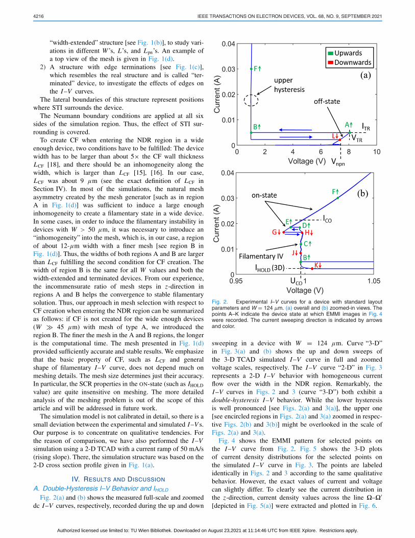
Fig. 2(a) and (b) shows the measured full-scale and zoomeddc I–V curves, respectively, recorded during the up and down
Fig. 2. Experimental I–V curves for a device with standard layoutparameters and W = 124 µm. (a) overall and (b) zoomed-in views. Thepoints A–K indicate the device state at which EMMI images in Fig. 4were recorded. The current sweeping direction is indicated by arrowsand color.
sweeping in a device with W = 124 μm. Curve “3-D”in Fig. 3(a) and (b) shows the up and down sweeps ofthe 3-D TCAD simulated I–V curve in full and zoomedvoltage scales, respectively. The I–V curve “2-D” in Fig. 3represents a 2-D I–V behavior with homogeneous currentflow over the width in the NDR region. Remarkably, theI–V curves in Figs. 2 and 3 (curve “3-D”) both exhibit adouble-hysteresis I –V behavior. While the lower hysteresisis well pronounced [see Figs. 2(a) and 3(a)], the upper one[see encircled regions in Figs. 2(a) and 3(a) zoomed in respec-tive Figs. 2(b) and 3(b)] might be overlooked in the scale ofFigs. 2(a) and 3(a).
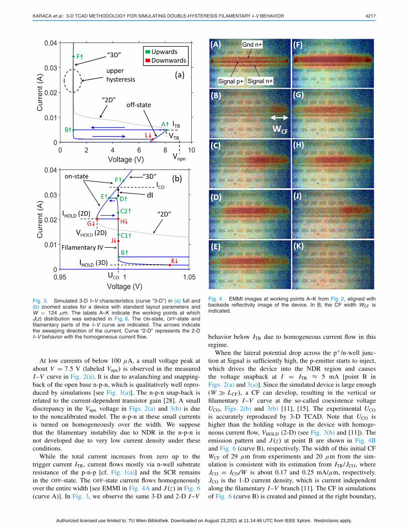
Fig. 4 shows the EMMI pattern for selected points onthe I–V curve from Fig. 2. Fig. 5 shows the 3-D plotsof current density distributions for the selected points onthe simulated I–V curve in Fig. 3. The points are labeledidentically in Figs. 2 and 3 according to the same qualitativebehavior. However, the exact values of current and voltagecan slightly differ. To clearly see the current distribution inthe z-direction, current density values across the line �–��[depicted in Fig. 5(a)] were extracted and plotted in Fig. 6.
Authorized licensed use limited to: TU Wien Bibliothek. Downloaded on August 23,2021 at 11:14:46 UTC from IEEE Xplore. Restrictions apply.
KARACA et al.: 3-D TCAD METHODOLOGY FOR SIMULATING DOUBLE-HYSTERESIS FILAMENTARY I–V BEHAVIOR 4217
Fig. 3. Simulated 3-D I–V characteristics (curve “3-D”) in (a) full and(b) zoomed scales for a device with standard layout parameters andW = 124 µm. The labels A–K indicate the working points at whichJ(z) distribution was extracted in Fig. 6. The ON-state, OFF-state andfilamentary parts of the I–V curve are indicated. The arrows indicatethe sweeping direction of the current. Curve “2-D” represents the 2-DI–V behavior with the homogeneous current flow.
At low currents of below 100 μA, a small voltage peak atabout V = 7.5 V (labeled Vnpn) is observed in the measuredI–V curve in Fig. 2(a). It is due to avalanching and snapping-back of the open base n-p-n, which is qualitatively well repro-duced by simulations [see Fig. 3(a)]. The n-p-n snap-back isrelated to the current-dependent transistor gain [28]. A smalldiscrepancy in the Vnpn voltage in Figs. 2(a) and 3(b) is dueto the noncalibrated model. The n-p-n at these small currentsis turned on homogeneously over the width. We supposethat the filamentary instability due to NDR in the n-p-n isnot developed due to very low current density under theseconditions.
While the total current increases from zero up to thetrigger current ITR, current flows mostly via n-well substrateresistance of the p-n-p [cf. Fig. 1(a)] and the SCR remainsin the OFF-state. The OFF-state current flows homogeneouslyover the entire width [see EMMI in Fig. 4A and J (z) in Fig. 6(curve A)]. In Fig. 3, we observe the same 3-D and 2-D I–V
Fig. 4. EMMI images at working points A–K from Fig. 2, aligned withbackside reflectivity image of the device. In B, the CF width WCF isindicated.
behavior below ITR due to homogeneous current flow in thisregime.
When the lateral potential drop across the p+/n-well junc-tion at Signal is sufficiently high, the p-emitter starts to inject,which drives the device into the NDR region and causesthe voltage snapback at I = ITR ≈ 5 mA [point B inFigs. 2(a) and 3(a)]. Since the simulated device is large enough(W � LCF), a CF can develop, resulting in the vertical orfilamentary I–V curve at the so-called coexistence voltageUCO, Figs. 2(b) and 3(b) [11], [15]. The experimental UCO
is accurately reproduced by 3-D TCAD. Note that UCO ishigher than the holding voltage in the device with homoge-neous current flow, VHOLD (2-D) (see Fig. 3(b) and [11]). Theemission pattern and J (z) at point B are shown in Fig. 4Band Fig. 6 (curve B), respectively. The width of this initial CFWCF of 29 μm from experiments and 20 μm from the sim-ulation is consistent with its estimation from ITR/JCO, whereJCO = ICO/W is about 0.17 and 0.25 mA/μm, respectively.JCO is the 1-D current density, which is current independentalong the filamentary I–V branch [11]. The CF in simulationsof Fig. 6 (curve B) is created and pinned at the right boundary,
Authorized licensed use limited to: TU Wien Bibliothek. Downloaded on August 23,2021 at 11:14:46 UTC from IEEE Xplore. Restrictions apply.

4218 IEEE TRANSACTIONS ON ELECTRON DEVICES, VOL. 68, NO. 9, SEPTEMBER 2021
Fig. 5. 3-D TCAD simulated total current density distribution inwidth-extended device at working points A–K, from Fig. 3. In (C),the working point corresponds to C1 in Figs. 3 and 6. The J(z) distributionis extracted along lines as Ω–Ω� indicated in (A).
but a CF creation at the left one is also possible if mesh oftype A is used over the whole device width. If a mesh oftype B is used, then the filament originates at the side of meshtype A since this region is wider than region B and the CFcan develop there more easily [15], [16].
At UCO, the ON-state region with the high current densityJCO = ICO/W (i.e., inside the CF) coexists with a low current
Fig. 6. Extracted distribution of simulated total current density alongthe device width at different working points (A–K) from Fig. 3. The J(z)distributions are extracted from data of Fig. 5, along lines such as Ω–Ω� inFig. 5A. The filament width WCF is indicated in curve B. The filamentarywall thickness LCF is indicated in curve C1.
density OFF-state elsewhere. The J (z) distribution can bedirectly related to the distribution of the B–E voltage of thep-n-p transistor, which controls the SCR action. The ON- andOFF-state regions in the CF are separated by a transitionregion called the filamentary wall having the thickness ofLCF (see Fig. 6 and [11], [15], and [18]). According to themodel in [15] and [16], LCF is an increasing function ofthe conductivity of SCR base (in our case the n-well) anda complex function of transistor gains. The value of UCO isdetermined by the balance between the ON- and OFF-stateregions at the filamentary wall [15], [16], [18].
Figs. 4C and 6 (curves C1 and C2) show the increase inWCF with increasing current I according to
WCF ≈ I
JCO(1)
where JCO remains constant.At still higher current (point D), the CF wall reaches the
device end, and the inhomogeneous filamentary state becomesunstable. The current conduction reverts to a homogeneousstate and the voltage jumps to point E. The voltage jumpD → E represents an “energy gain” related to the disappear-ance of CF wall [11], [15]. The current difference dI betweenpoint D and the point at the ON-state I–V curve at UCO
[see Fig. 3(b)] is related to a missing current flow over theregion with a thickness of LCF nearly.
Above point E, the current flows homogeneously[see Figs. 4F and 6 (curve F)]. When the current decreases,the homogeneous current distribution stays stable until thepoint G [see Figs. 4G and 6 (curve G)]. Notice that the 3-DI–V (curve “3-D”) and 2-D I–V (curve “2-D”) characteristicsin Fig. 3(b) are identical in the homogeneous ON-state. Theupper hysteresis HDEG [see Fig. 3(b)] originates because,at point D, the parameter dI is related to LCF, while,at point G, the device enters the NDR region, which dependson the shape of the 2-D I–V curve. These two SCRcharacteristics are not directly related to each other [15], [16].At the current region of the upper hysteresis, there may existtwo different voltages for the same applied current depending
Authorized licensed use limited to: TU Wien Bibliothek. Downloaded on August 23,2021 at 11:14:46 UTC from IEEE Xplore. Restrictions apply.

KARACA et al.: 3-D TCAD METHODOLOGY FOR SIMULATING DOUBLE-HYSTERESIS FILAMENTARY I–V BEHAVIOR 4219
on whether the device conducts homogeneously over thewidth (region G–E), or CF is created (H–D). These two statesdepend on sweeping prehistory.
Below point G, the device enters the NDR region, and a CFis created. The voltage jumps to point H on the filamentaryI–V curve. The EMMI and J (z) patterns at point H show thepronounced filamentary state [see Figs. 4H and 6 (curve H)].Interestingly, in this simulation, the CF at point H is pinned atthe left boundary, which is the opposite side of the devicecompared to the side that the current rose initially (com-pare curves H and B–D in Fig. 6). In this particular case,the position of mesh type B coincides with the CF position.However, the CF can be pinned also at the right boundary,depending on mesh details, current step, and so on, indicatingthat numerical nuances matter. However, what is important isthat the CF is always created for devices larger than 50 μm(so for W > 5 × LCF) at either the left or right positions, andso a stable filamentary solution is obtained.
When the current decreases further, WCF decreases (see datain Figs. 4 and 6 for point J) until point K, the currentcalled 3-D IHOLD, or IHOLD (3-D). Notice that the voltage atpoint K is only slightly higher than UCO; consider the apparentamplifying effect of the zoomed scale in Figs. 2(b) and 3(b).At this point, the filamentary I–V curve enters its unstablebranch (see line “F” in Fig. 1 in [11] for details). IHOLD
(3-D) is the lowest current where the SCR still operates inthe ON-state. We emphasize that this is the IHOLD value thathas to be considered in latch-up considerations. The EMMIand J (z) in Figs. 4 and 6, respectively, show a small CFat the structure edge at working point K. Its width WCF isdetermined by LCF. LCF estimation from IHOLD (3-D)/JCO ≈9 μm is consistent with the 20%–80% variation in J (z)(see Fig. 6). Due to the filamentary nature of conduction,IHOLD (3-D) of about 2 mA is much lower than IHOLD
(2-D) ≈ 20 mA. However, the current density inside the CFof nearly JCO = 0.25 mA/μm is higher compared to that atIHOLD (2-D) of IHOLD (2-D)/W ≈ 0.16 mA/μm. This showsthat the SCR action in CF at IHOLD (3-D) is supported by asufficiently high current density.
Below point K, the self-sustaining operation of SCR in theCF is not possible anymore, and the device returns to a modewhere the current only flows through the open base n-p-n [seepoint L in Figs. 2(a) and 3(a)], where the current flows againhomogeneously (not shown).
We remark that the lower hysteresis LABK (see Fig. 3)is due to the fact that, while ITR at point A is related tohomogeneous current flow in the OFF-state, the property ofthe SCR at point K is related to the filamentary state.
B. Geometry Dependence of IHOLD
The theory predicts that the filamentary instability occurs indevices wider than about 5×LCF [18], which is about 45 μmin our case. Therefore, we have carried out I–V measurementsof available devices with W in the 31.3–185.8-μm range, andwe performed simulations of both types of devices (width-extended and terminated) with W in the 2–185-μm range.Thus, both regimes below and above 5 × LCF are covered.
Fig. 7. (a) Experimental and (b) 3-D TCAD simulated I–V curves for thewidth-extended device with the device width W as a parameter. For bettervisibility, the curves in (a) and (b) are fanned out with a 20-mV distancebetween two curves. The VCO value for each curve does not depend onthe device width W. (c) Measured and simulated IHOLD values extractedfrom data of (a) and (b). The data points for the terminated device arealso included. In the case of no CF creation for W < 50 µm, the value ofIHOLD (2-D) is considered for IHOLD.
Examples of experimental and 3-D-simulated I–V curvesfor width-extended devices are given in Fig. 7(a) and (b),respectively. For better visibility, the curves for increasingwidth are subsequently horizontally fanned out with a 20-mVdistance between two curves. This means that the UCO valuedoes not depend on the device width W . The IHOLD valuesextracted from the I–V data of Fig. 7(a) and (b) are given inFig. 7(c). In experiments, IHOLD for W = 31.3 μm is slightlysmaller than the values for W > 60 μm, which are width-independent. The simulated IHOLD (3-D) shows, first, a linearincrease with W until W = 40 μm, and then, it jumps to aconstant value for W > 45 μm. For W < 45 μm, the device
Authorized licensed use limited to: TU Wien Bibliothek. Downloaded on August 23,2021 at 11:14:46 UTC from IEEE Xplore. Restrictions apply.

4220 IEEE TRANSACTIONS ON ELECTRON DEVICES, VOL. 68, NO. 9, SEPTEMBER 2021
Fig. 8. 3-D TCAD simulated I–V curve in width-extended and terminateddevice in (a) full and (b) zoomed scales. W = 124 µm. The thick arrowin (b) indicates the early transition from ON-state to filamentary state inthe terminated device. The small horizontal arrows indicate the currentsweeping direction.
is not large enough to induce the NDR instability, which isconsistent with the 5 × LCF criterion. For W < 45 μm,the values of IHOLD from 2-D and 3-D TCAD are identical,and thus, IHOLD scales linearly with W . This can be directlyseen in the I–V curves where the double-hysteresis and idealfilamentary I–V behavior is not formed for the device withW = 31.3 μm in experiments [see Fig. 7(a)] and for W =10 μm and W = 30 μm in simulations [see Fig. 7(b)]. Thus,the double-hysteresis filamentary I–V in Fig. 7(a) and (b) isobserved only for W > 5 × LCF. We notice that the lack ofdevices with widths in the 30–50-μm range prevents us to seethe linearly increasing part in the IHOLD–W dependence in theexperimental data.
Fig. 8 compares the 3-D I–V curves of the width-extended and terminated structure for W = 124 μm. Whilethe trigger parameters are nearly identical for this width[see Fig. 8(a)], IHOLD increases by 30% for the terminateddevice [see Fig. 8(b)]. Furthermore, one observes a transitionfrom the ON-state to filamentary I–V curve at higher currentsin the down-sweep than in the terminated device, as indicatedby the thick arrow in Fig. 8(b). The termination likely inducesan inhomogeneity, which facilitates an earlier transition to thefilamentary state.
The simulated IHOLD values in the terminated device as afunction of W are added in Fig. 7(c) (see green squares). Thecritical device width for the CF creation of about 45 μm alsofulfills the 5 × LCF criterion. One can remark that IHOLD inthe terminated device is higher than that in the width-extendeddevice, and this difference is nearly width-independent for
Fig. 9. (a) and (b) Experimental and (c) and (d) 3-D TCAD simulated I–Vcurves for the width-extended device as a function of (a) L and (c) nearVTR and (b) and (d) near UCO voltages. (e) Extracted measured IHOLDand simulated values of IHOLD (3-D) and IHOLD (2-D) as a function of L.
W > 60 μm. This is attributed to an additional current flowaround the edge. The IHOLD values for terminated devices alsomatch better to experimental values. However, this increased
Authorized licensed use limited to: TU Wien Bibliothek. Downloaded on August 23,2021 at 11:14:46 UTC from IEEE Xplore. Restrictions apply.

KARACA et al.: 3-D TCAD METHODOLOGY FOR SIMULATING DOUBLE-HYSTERESIS FILAMENTARY I–V BEHAVIOR 4221
Fig. 10. Simulated 3-D I–V curves for the width-extended device in (a) fulland (b) zoomed scales with Lpn as parameters. (c) Extracted simulatedvalues of IHOLD (3-D) and IHOLD (2-D) as a function of Lpn.
accuracy is accompanied by an increased simulation time.Since IHOLD for the width-extended device is lower than forthe terminated device, the former represents, thus, the worstcase scenario in IHOLD estimation. For the latter and compu-tational time-saving reasons, IHOLD for other layout variationshas been evaluated only for the width-extended device withW = 50 μm. For this width, a CF is certain to be created.
Fig. 9(a)–(d) shows the experimental and simulatedI–V curves with L as a parameter. Fig. 9(a) and (c) shows theI–V curve near the VTR and Fig. 9(b) and (d) near UCO. Sinceincreasing L enhances the base width of the n-p-n, its gaindecreases, and the open base breakdown voltage of the n-p-nshifts slightly to higher values. As well, due to the same reasonthe VHOLD (2-D) shifts to higher voltage with increasing L.UCO follows this trend. This is observed in both experimentand simulation. The extracted values of IHOLD from 2-D and3-D simulations are given in Fig. 9(e). While IHOLD (2-D)increases with L, IHOLD (3-D) is L-independent and muchlower than IHOLD (2-D).
Fig. 10(a) and (b) shows the simulated I–V curves with Lpn
as a parameter near VTR and near UCO, respectively. For this
layout variation, there are no experimental data. The value ofITR for the studied layout range does not depend much on Lpn
[see Fig. 10(a)]. ITR depends on total n-well resistance belowp+ and in the region of length Lpn [see Fig. 1(a)]. However,it is mainly the n-well resistance part of width dsub below thep-well, which controls the forward biasing of the p+/n-welljunction necessary for p-n-p triggering. When a potential dropof about 0.7 V occurs on this resistance part the SCR triggers.Since dsub is Lpn-independent and the net n-well doping ofthis region is lower than that in the region of the lengthLpn, the value of VTR also does not depend much on Lpn.VHOLD (2-D) decreases as Lpn increases due to an increasedcontribution of the vertical p-n-p current path for larger Lpn.The vertical current path of the p-n-p is discussed in [24].
The extracted values of IHOLD from 2-D and 3-D simulationsare shown in Fig. 10(c). While IHOLD (2-D) decreases withLpn, IHOLD (3-D) is lower and layout-independent.
It is challenging to explain the independence of IHOLD
(3-D) on layout parameters in Figs. 9(e) and 10(c) in simpleand intuitive terms. In general, we relate it to the high injectioncondition in the CF (the SCR is in the ON-state there), wherethe details of geometry do not play a significant role. At highinjection, a dense electron-hole plasma floods the entire deviceactive region and controls the transport. In addition, in thesefloating-base devices, a conductivity modulation takes placein the low-doped p-sub in between the Ground n+-regionand deep p-well [4], [24], which complicates the pictureeven more. Moreover, although UCO, which is related toIHOLD (3-D), can be modeled analytically only for simple1-D doping profile structures [15], [16]. There is no theory,and therefore, the intuitive view for how UCO depends onthe SCR structure parameters with 2-D doping profiles. Theunderstanding of the complexity of this problem will be treatedin future works.
V. CONCLUSION
Using quasi-dc current up and down sweeps in 3-D TCAD,we are able to simulate the double-hysteresis I–V curve andholding current IHOLD in ESD protection SCRs. The shape ofthe I–V curve has been related to spatial distribution of thecurrent density in the width direction. The value of simulatedIHOLD in the devices with width-extended 2-D profiles is lowerthan that in the terminated devices. The simulation of width-extended devices represents, thus, a worst case scenario inthe 3-D TCAD estimation of IHOLD. IHOLD increases with thedevice width for W smaller than five times the filamentarywall thickness since no CFs are formed. For larger W , CFsare formed, and IHOLD becomes W -independent. Importantly,while IHOLD determined from 3-D TCAD is typically indepen-dent of the layout parameters, the value of IHOLD determinedfrom 2-D TCAD strongly depends on them and is typicallyseveral times higher. Thus, 3-D TCAD has to be used for thelatch-up safe ESD protection design of IHOLD.
APPENDIX
The self-heating effect has been estimated using the 2-Dthermodynamic simulation of the structure shown in Fig. 1(a).
Authorized licensed use limited to: TU Wien Bibliothek. Downloaded on August 23,2021 at 11:14:46 UTC from IEEE Xplore. Restrictions apply.

4222 IEEE TRANSACTIONS ON ELECTRON DEVICES, VOL. 68, NO. 9, SEPTEMBER 2021
STI and the additional silicon on the substrate and the lateralsides have been considered. The substrate thickness was240 μm, and the lateral chip extension beyond STI was200 μm on each side. The current density was chosen atJCO = ICO/W [see Fig. 3(b)], which corresponds to that inCF. The simulated maximum temperature rise at steady statewas about 15 K, which represents worst case estimate. Sincethe 2-D simulation considers zero heat flow in the z-direction(i.e., infinite extended heat source in the z-direction), we mayexpect that the temperature in the 3-D structure with finitewidth will be even lower.
REFERENCES
[1] J. Di Sarro, K. Chatty, R. Gauthier, and E. Rosenbaum, “Study of designfactors affecting turn-on time of silicon controlled rectifiers (SCRS)in 90 and 65 nm bulk CMOS technologies,” in Proc. IEEE Int. Rel.Phys. Symp. Proc., San Jose, CA, USA, Mar. 2006, pp. 163–168, doi:10.1109/RELPHY.2006.251210.
[2] G. Notermans et al., “Design of an on-board ESD protection forUSB3 applications,” IEEE Trans. Device Mater. Rel., vol. 16, no. 4,pp. 504–512, Dec. 2016, doi: 10.1109/TDMR.2016.2622400.
[3] W. Soldner et al., “RF ESD protection strategies: Codesign vs. low-C protection,” Microelectron. Rel., vol. 47, no. 7, pp. 1008–1015,Jul. 2007, doi: 10.1016/j.microrel.2006.11.007.
[4] G. Notermans, H.-M. Ritter, S. Holland, and D. Pogany, “Model-ing dynamic overshoot in ESD protections,” in Proc. 40th Electr.Overstress/Electrostatic Discharge Symp. (EOS/ESD), Reno, NV, USA,Sep. 2018, pp. 1–9, doi: 10.23919/EOS/ESD.2018.8509781.
[5] S. H. Voldman, Latchup. Hoboken, NJ, USA: Wiley, 2008.[6] M.-D. Ker, S.-F. Hsu, Transient-Induced Latchup in CMOS Integrated
Circuits. Hoboken, NJ, USA: Wiley, 2009.[7] Y.-C. Huang and M.-D. Ker, “A latchup-immune and robust SCR
device for ESD protection in 0.25-μm 5-V CMOS process,” IEEEElectron Device Lett., vol. 34, no. 5, pp. 674–676, May 2013, doi:10.1109/LED.2013.2252456.
[8] M. P. Mergens, C. C. Russ, K. G. Verhaege, J. Armer, P. C. Jozwiak, andR. Mohn, “High holding current SCRs (HHI-SCR) for ESD protectionand latch-up immune IC operation,” Microelectron. Rel., vol. 43, no. 7,pp. 993–1000, 2003, doi: 10.1016/S0026-2714(03)00125-2.
[9] H. Liang, X. Bi, X. Gu, H. Cao, and Y. Zhang, “Investigation onLDMOS-SCR with high holding current for high voltage ESD pro-tection,” Microelectron. Rel., vol. 61, pp. 120–124, Jun. 2016, doi:10.1016/j.microrel.2016.01.016.
[10] S. Bart, B. Ilse, M. Olivier, and K. Bart, “On-chip ESD protection withimproved high holding current SCR (HHISCR) achieving IEC 8 kVcontact system level,” in Proc. IEEE Electr. Overstress/ElectrostaticDischarge Symp. (EOS/ESD), Reno, NV, USA, Nov. 2010,pp. 1–10.
[11] D. Pogany et al., “Measuring holding voltage related to homogeneouscurrent flow in wide ESD protection structures using multilevel TLP,”IEEE Trans. Electron Devices, vol. 58, no. 2, pp. 411–418, Feb. 2011,doi: 10.1109/TED.2010.2093143.
[12] H. L. Grubin, V. V. Mitin, E. Schöll, and M. P. Shaw, The Physicsof Instabilities in Solid State Electron Devices. New York, NY, USA:Springer, 2013.
[13] K. Esmark, “Device simulation of ESD protection elements,” Ph.D.dissertation, ETH Zurich, Zurich, Switzerland, 2001, doi: 10.3929/ethz-a-004317494.
[14] M. Denison et al., “Moving current filaments in integrated DMOStransistors under short-duration current stress,” IEEE Trans. Elec-tron Devices, vol. 51, no. 10, pp. 1695–1703, Oct. 2004, doi:10.1109/TED.2004.835978.
[15] I. Varlamov, V. Osipov, and E. Poltoratskii, “Current fillamentation in afour-layer structure,” Sov. Phys. Semicond., vol. 3 no. 8, pp. 978–982,1970.
[16] I. V. Varlamov and V. V. Osipov, “Current filamentation in pnpn-structures,” Sov. Phys. Semicond., vol. 3, no. 7, pp. 803–911, 1970.
[17] C. Fleury, G. Notermans, H.-M. Ritter, and D. Pogany, “TIM,EMMI and 3D TCAD analysis of discrete-technology SCRs,”Microelectron. Rel., vols. 76–77, pp. 698–702, Sep. 2017, doi:10.1016/j.microrel.2017.06.070.
[18] M. Meixner, P. Rodin, E. Schöll, and A. Wacker, “Lateral currentdensity fronts in globally coupled bistable semiconductors with S- orZ-shaped current voltage characteristics,” Eur. Phys. J. B, vol. 13, no. 1,pp. 157–168, Jan. 2000, doi: 10.1007/s100510050019.
[19] M. Litzenberger, C. Furbock, D. Pogany, E. Gornik, K. Esmark, andH. Gossner, “Investigation of 3D phenomena in the triggering of gg-nMOS electrostatic discharge protection devices,” in Proc. 30th Eur.Solid-State Device Res. Conf., Cork, Ireland, Sep. 2000, pp. 520–523,doi: 10.1109/ESSDERC.2000.194829.
[20] C. Musshoff, H. Wolf, H. Gieser, P. Egger, and X. Guggenmos,“Risetime effects of HBM and square pulses on the failure thresholdsof GGNMOS-transistors,” Microelectron. Rel., vol. 36, nos. 11–12,pp. 1743–1746, Nov. 1996, doi: 10.1016/0026-2714(96)00188-6.
[21] C. Russ, K. Bock, M. Rasras, I. De Wolf, G. Groeseneken, andH. E. Maes, “Non-uniform triggering of gg-nMOSt investigated bycombined emission microscopy and transmission line pulsing,” in Proc.Electr. Overstress/ Electrostatic Discharge Symp., Reno, NV, USA,Oct. 1998, pp. 177–186, doi: 10.1109/EOSESD.1998.737037.
[22] M. Gartner, D. Vietzke, D. Reznik, M. Stoisiek, K. G. Oppermann,and W. Gerlach, “Bistability and hysteresis in the characteristics ofsegmented-anode lateral IGBTs,” IEEE Trans. Electron Devices, vol. 45,no. 7, pp. 1575–1579, Jul. 1998, doi: 10.1109/16.701491.
[23] H. Karaca et al., “Triggering of multi-finger and multi-segment SCRsnear the holding voltage studied by emission microscopy under DC con-ditions,” presented at the Int. ESD Workshop (ESDA/IEW), Hamburg,Germany, May 2021.
[24] H. Karaca et al., “Simultaneous and sequential triggering in multi-finger floating-base SCRs depending on TLP pulse rise time,” IEEETrans. Device Mater. Rel., vol. 20, no. 4, pp. 632–640, Dec. 2020, doi:10.1109/TDMR.2020.3033618.
[25] K.-H. Oh, C. Duvvury, K. Banerjee, and R. W. Dutton, “Analysis ofnonuniform ESD current distribution in deep submicron NMOS tran-sistors,” IEEE Trans. Electron Devices, vol. 49, no. 12, pp. 2171–2182,Dec. 2002, doi: 10.1109/TED.2002.805049.
[26] P. Salome, C. Leroux, J. P. Chante, P. Crevel, and G. Reimbold, “Studyof a 3D phenomenon during ESD stresses in deep submicron CMOStechnologies using photon emission tool,” in Proc. IEEE 35th Annu.Int. Rel. Phys. Symp., Denver, CO, USA, Apr. 1997, pp. 325–332, doi:10.1109/RELPHY.1997.584282.
[27] T.C.A.D. Industry-Standard Process and Device Simulators, SENTAU-RUS, Synopsys. Inc., Mountain View, CA, USA, May 2012.
[28] B. El-Kareh and R. J. Bombard, Introduction to VLSI Silicon Devices:Physics, Technology and Characterization, vol. 10. New York, NY, USA:Springer, 2012.
Authorized licensed use limited to: TU Wien Bibliothek. Downloaded on August 23,2021 at 11:14:46 UTC from IEEE Xplore. Restrictions apply.