Embed Size (px)
Citation preview
2.93.13.33.53.73.94.14.34.54.74.95.15.35.55.5
0
10
20
30
40
50
60
70
80
90
100
0.1 0
.2 0.4 0
.8 1.6 3
.2 6.3 12
.6
25
.1
50
.1
10
0.0
19
9.4
39
7.9
VI - Input Voltage - V
Eff
icie
nc
y-
%
IO - Output Current - mA
.
V = 5.0 VO
CI
CO
L
VIN
EN
VOUT
GND
L VOUT
= 5.0 VDC/DC Converter
TPS81256SIP
ENABLE
GND
4.7µF16V X5R (0603)
VIN
2.5 V .. 4.85 V
Product
Folder
Order
Now
Technical
Documents
Tools &
Software
Support &Community
An IMPORTANT NOTICE at the end of this data sheet addresses availability, warranty, changes, use in safety-critical applications,intellectual property matters and other important disclaimers. PRODUCTION DATA.
TPS81256SLVSAZ9D –JUNE 2012–REVISED FEBRUARY 2018
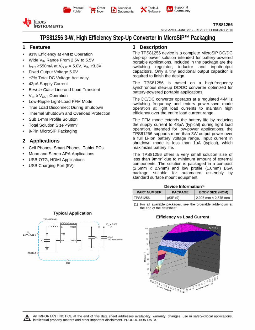
TPS81256 3-W, High Efficiency Step-Up Converter In MicroSiP™ Packaging
1
1 Features1• 91% Efficiency at 4MHz Operation• Wide VIN Range From 2.5V to 5.5V• IOUT ≥550mA at VOUT = 5.0V, VIN ≥3.3V• Fixed Output Voltage 5.0V• ±2% Total DC Voltage Accuracy• 43µA Supply Current• Best-in-Class Line and Load Transient• VIN ≥ VOUT Operation• Low-Ripple Light-Load PFM Mode• True Load Disconnect During Shutdown• Thermal Shutdown and Overload Protection• Sub 1-mm Profile Solution• Total Solution Size <9mm2
• 9-Pin MicroSiP Packaging
2 Applications• Cell Phones, Smart-Phones, Tablet PCs• Mono and Stereo APA Applications• USB-OTG, HDMI Applications• USB Charging Port (5V)
3 DescriptionThe TPS81256 device is a complete MicroSiP DC/DCstep-up power solution intended for battery-poweredportable applications. Included in the package are theswitching regulator, inductor and input/outputcapacitors. Only a tiny additional output capacitor isrequired to finish the design.
The TPS81256 is based on a high-frequencysynchronous step-up DC/DC converter optimized forbattery-powered portable applications.
The DC/DC converter operates at a regulated 4-MHzswitching frequency and enters power-save modeoperation at light load currents to maintain highefficiency over the entire load current range.
The PFM mode extends the battery life by reducingthe supply current to 43μA (typical) during light loadoperation. Intended for low-power applications, theTPS81256 supports more than 3W output power overa full Li-Ion battery voltage range. Input current inshutdown mode is less than 1µA (typical), whichmaximizes battery life.
The TPS81256 offers a very small solution size ofless than 9mm2 due to minimum amount of externalcomponents. The solution is packaged in a compact(2.6mm x 2.9mm) and low profile (1.0mm) BGApackage suitable for automated assembly bystandard surface mount equipment.
Device Information(1)
PART NUMBER PACKAGE BODY SIZE (NOM)TPS81256 µSIP (9) 2.925 mm × 2.575 mm
(1) For all available packages, see the orderable addendum atthe end of the datasheet.
Typical ApplicationEfficiency vs Load Current

2
TPS81256SLVSAZ9D –JUNE 2012–REVISED FEBRUARY 2018 www.ti.com
Product Folder Links: TPS81256
Submit Documentation Feedback Copyright © 2012–2018, Texas Instruments Incorporated
Table of Contents1 Features .................................................................. 12 Applications ........................................................... 13 Description ............................................................. 14 Revision History..................................................... 25 Device Options....................................................... 36 Pin Configuration and Functions ......................... 37 Specifications......................................................... 4
7.1 Absolute Maximum Ratings ...................................... 47.2 ESD Ratings ............................................................ 47.3 Recommended Operating Conditions....................... 47.4 Thermal Information .................................................. 57.5 Electrical Characteristics........................................... 57.6 Typical Characteristics .............................................. 6
8 Detailed Description .............................................. 98.1 Overview ................................................................... 98.2 Functional Block Diagram ......................................... 98.3 Feature Description................................................... 98.4 Device Functional Modes........................................ 11
9 Application and Implementation ........................ 129.1 Application Information............................................ 129.2 Typical Application ................................................. 129.3 System Examples .................................................. 15
10 Power Supply Recommendations ..................... 1711 Layout................................................................... 17
11.1 Layout Guidelines ................................................. 1711.2 Layout Example .................................................... 1711.3 Surface Mount Information ................................... 1811.4 Thermal and Reliability Information ...................... 18
12 Device and Documentation Support ................. 2012.1 Device Support...................................................... 2012.2 Community Resources.......................................... 2012.3 Trademarks ........................................................... 2012.4 Electrostatic Discharge Caution............................ 2012.5 Glossary ................................................................ 20
13 Mechanical, Packaging, and OrderableInformation ........................................................... 21
4 Revision HistoryNOTE: Page numbers for previous revisions may differ from page numbers in the current version.
Changes from Revision C (February 2016) to Revision D Page
• Updated package drawing.................................................................................................................................................... 22
Changes from Revision B (February 2015) to Revision C Page
• Reversed D & E dimensions in to match MECHANICAL DATA drawing; and, changed "8-bump" to "9-bump" in thedescription. ........................................................................................................................................................................... 21
• Added Community Resources section ................................................................................................................................ 21
Changes from Revision A (August 2013) to Revision B Page
• Added Device Information and ESD Ratings tables, Feature Description section, Device Functional Modes,Application and Implementation section, System Examples, Power Supply Recommendations section, Device andDocumentation Support section, and Mechanical, Packaging, and Orderable Information section. .................................... 1
• Changed the pinout drawing to match the device orientation shown on the MECHANICAL DATA drawing. ...................... 3• Changed SIP Package "Top View" image orientation to correctly match "YML LSB" symbolization with pin A1. .............. 21
Changes from Original (June 2012) to Revision A Page
• Added animated performance characteristics table ............................................................................................................... 6• Deleted MLCC capacitor B1 life documentation................................................................................................................... 19

SIP-9(TOP VIEW)
SIP-9(BOTTOM VIEW)
C1
C2
C3
B1
B2
B3
GND
GND
VOUT
A1
A3VOUT
VIN
VIN
A1
A3
B1
B2
B3 VOUT
VIN
VINGND
C3VOUT
GND
C1
C2A2
EN
A2
EN
3
TPS81256www.ti.com SLVSAZ9D –JUNE 2012–REVISED FEBRUARY 2018
Product Folder Links: TPS81256
Submit Documentation FeedbackCopyright © 2012–2018, Texas Instruments Incorporated
5 Device Options
PART NUMBER OUTPUT VOLTAGE PACKAGE MARKINGCHIP CODE
TPS81256 5.0V TT
6 Pin Configuration and Functions
SIP Package9-Pin µSIP
Pin FunctionsPIN
I/O DESCRIPTIONNAME NO.
EN B2 IThis is the enable pin of the device. Connecting this pin to ground forces the device into shutdownmode. Pulling this pin high enables the device. This pin must not be left floating and must beterminated.
GND A1, A2, B1 Ground pin.VIN C1, C2 I Power supply input.VOUT A3, B3, C3 O Boost converter output.

4
TPS81256SLVSAZ9D –JUNE 2012–REVISED FEBRUARY 2018 www.ti.com
Product Folder Links: TPS81256
Submit Documentation Feedback Copyright © 2012–2018, Texas Instruments Incorporated
(1) Stresses beyond those listed under Absolute Maximum Ratings may cause permanent damage to the device. These are stress ratingsonly, which do not imply functional operation of the device at these or any other conditions beyond those indicated under RecommendedOperating Conditions. Exposure to absolute-maximum-rated conditions for extended periods may affect device reliability.
(2) All voltages are with respect to network ground terminal.(3) Limit the junction and the (top side) inductor case temperature to 110°C, limit the (top side) capacitor case temperature to 85°C for
2000h operation at maximum output power. Contact TI for more details on lifetime estimation.(4) Limit the (top side) inductor case temperature to 140°C and the (top side) capacitor temperature to 115°C for 100h operation. Contact TI
for more details on lifetime estimation.(5) In applications where high power dissipation and/or poor package thermal resistance is present, the maximum ambient temperature may
have to be derated. Maximum ambient temperature (TA(max)) is dependent on the maximum operating junction temperature (TJ(max)), themaximum power dissipation of the device in the application (PD(max)), and the junction-to-ambient thermal resistance of the part/packagein the application (θJA), as given by the following equation: TA(max)= TJ(max)–(θJA X PD(max)). To achieve optimum performance, it isrecommended to operate the device with a maximum junction temperature of 125°C, a maximum inductor case temperature of 125°Cand a maximum capacitor case temperature of 85°C.
7 Specifications
7.1 Absolute Maximum Ratingsover operating free-air temperature range (unless otherwise noted) (1)
MIN MAX UNITInput voltage Voltage at VIN (2), VOUT (2), EN (2) –0.3 6 V
Input currentContinuous average current into VIN (3) 1.05 APulsed current into VIN (4) 1.3 A
Power dissipation Internally limitedOperating temperature, TA
(3) (4) (5) –40 85 °COperating virtual junction temperature, TJ –40 150 °CStorage temperature, Tstg –55 125 °C
(1) JEDEC document JEP155 states that 500-V HBM allows safe manufacturing with a standard ESD control process.(2) JEDEC document JEP157 states that 250-V CDM allows safe manufacturing with a standard ESD control process.
7.2 ESD RatingsVALUE UNIT
V(ESD) Electrostatic discharge
Human body model (HBM), per ANSI/ESDA/JEDEC JS-001, allpins (1)
±2000
VCharged device model (CDM), per JEDEC specificationJESD22-C101, all pins (2)
±1000
Machine Model - (MM) ±200
7.3 Recommended Operating Conditionsover operating free-air temperature range (unless otherwise noted)
MIN NOM MAX UNITVI Input voltage range 2.5 5.5 VRL Minimum resistive load for start-up (VI ≤ 4.8V) 65 Ω
CEXT Output capacitance 2 30 µFTA Ambient temperature –40 85 °CTJ Operating junction temperature –40 125 °CTCASE_IND Operating inductor case temperature 125 °CTCASE_CAP Operating capacitor case temperature 85 °C
5
TPS81256www.ti.com SLVSAZ9D –JUNE 2012–REVISED FEBRUARY 2018
Product Folder Links: TPS81256
Submit Documentation FeedbackCopyright © 2012–2018, Texas Instruments Incorporated
(1) Thermal data have been simulated with high-K board (per JEDEC standard).
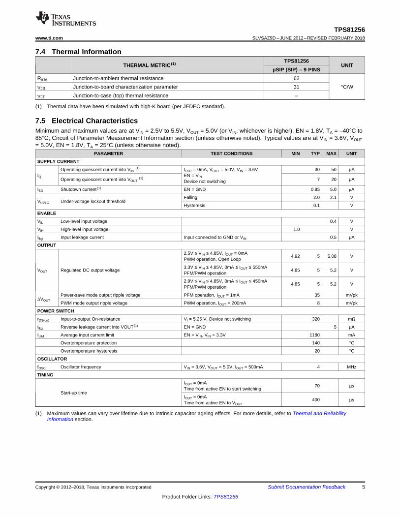
7.4 Thermal Information
THERMAL METRIC (1) TPS81256UNIT
µSIP (SIP) – 9 PINSRθJA Junction-to-ambient thermal resistance 62
°C/WψJB Junction-to-board characterization parameter 31ψJT Junction-to-case (top) thermal resistance –
(1) Maximum values can vary over lifetime due to intrinsic capacitor ageing effects. For more details, refer to Thermal and ReliabilityInformation section.
7.5 Electrical CharacteristicsMinimum and maximum values are at VIN = 2.5V to 5.5V, VOUT = 5.0V (or VIN, whichever is higher), EN = 1.8V, TA = –40°C to85°C; Circuit of Parameter Measurement Information section (unless otherwise noted). Typical values are at VIN = 3.6V, VOUT= 5.0V, EN = 1.8V, TA = 25°C (unless otherwise noted).
PARAMETER TEST CONDITIONS MIN TYP MAX UNIT
SUPPLY CURRENT
IQOperating quiescent current into VIN
(1) IOUT = 0mA, VOUT = 5.0V, VIN = 3.6VEN = VINDevice not switching
30 50 µA
Operating quiescent current into VOUT(1) 7 20 µA
ISD Shutdown current (1) EN = GND 0.85 5.0 μA
VUVLO Under-voltage lockout thresholdFalling 2.0 2.1 V
Hysteresis 0.1 V
ENABLE
VIL Low-level input voltage 0.4 V
VIH High-level input voltage 1.0 V
Ilkg Input leakage current Input connected to GND or VIN 0.5 µA
OUTPUT
VOUT Regulated DC output voltage
2.5V ≤ VIN ≤ 4.85V, IOUT = 0mAPWM operation. Open Loop 4.92 5 5.08 V
3.3V ≤ VIN ≤ 4.85V, 0mA ≤ IOUT ≤ 550mAPFM/PWM operation 4.85 5 5.2 V
2.9V ≤ VIN ≤ 4.85V, 0mA ≤ IOUT ≤ 450mAPFM/PWM operation 4.85 5 5.2 V
ΔVOUTPower-save mode output ripple voltage PFM operation, IOUT = 1mA 35 mVpk
PWM mode output ripple voltage PWM operation, IOUT = 200mA 8 mVpk
POWER SWITCH
rDS(on) Input-to-output On-resistance VI = 5.25 V. Device not switching 320 mΩ
Ilkg Reverse leakage current into VOUT (1) EN = GND 5 µA
ILIM Average input current limit EN = VIN. VIN = 3.3V 1180 mA
Overtemperature protection 140 °C
Overtemperature hysteresis 20 °C
OSCILLATOR
fOSC Oscillator frequency VIN = 3.6V, VOUT = 5.0V, IOUT = 500mA 4 MHz
TIMING
Start-up time
IOUT = 0mATime from active EN to start switching 70 µs
IOUT = 0mATime from active EN to VOUT
400 µs
0.1 1 10 100 1000
I - Output Current - mAO
50
55
60
65
70
75
80
85
90
95
100
Eff
icie
ncy -
%
V = 4.5 VI
V = 4.2 VI
V = 3.6 VI
V = 2.7 VI
V = 2.9 VI
V = 3.3I
V = 5 V,
PFM/PWM OperationO
Eff
icie
nc
y -
%
70
72
74
76
78
80
82
84
86
88
90
92
94
96
98
100
2.7 2.9 3.1 3.3 3.5 3.7 3.9 4.1 4.3 4.5
V - Input Voltage - VI
I = 100 mAO
I = 500 mAO
I = 1 mAO
I = 10 mAO
V = 5 V,
PFM/PWM OperationO
I = 300 mAO
6
TPS81256SLVSAZ9D –JUNE 2012–REVISED FEBRUARY 2018 www.ti.com
Product Folder Links: TPS81256
Submit Documentation Feedback Copyright © 2012–2018, Texas Instruments Incorporated
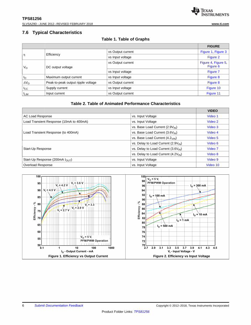
7.6 Typical CharacteristicsTable 1. Table of Graphs
FIGURE
η Efficiencyvs Output current Figure 1, Figure 3vs Input voltage Figure 2
VO DC output voltagevs Output current Figure 4, Figure 5,
Figure 6vs Input voltage Figure 7
IO Maximum output current vs Input voltage Figure 8ΔVO Peak-to-peak output ripple voltage vs Output current Figure 8ICC Supply current vs Input voltage Figure 10ILIM Input current vs Output current Figure 11
Table 2. Table of Animated Performance CharacteristicsVIDEO
AC Load Response vs. Input Voltage Video 1Load Transient Response (10mA to 400mA) vs. Input Voltage Video 2
Load Transient Response (to 400mA)vs. Base Load Current (2.9VIN) Video 3vs. Base Load Current (3.6VIN) Video 4vs. Base Load Current (4.2VIN) Video 5
Start-Up Responsevs. Delay to Load Current (2.9VIN) Video 6vs. Delay to Load Current (3.6VIN) Video 7vs. Delay to Load Current (4.2VIN) Video 8
Start-Up Response (200mA IOUT) vs. Input Voltage Video 9Overload Response vs. Input Voltage Video 10
Figure 1. Efficiency vs Output Current Figure 2. Efficiency vs Input Voltage
2.9 3.1 3.3 3.5 3.7 3.9 4.1 4.3 4.5 4.7 4.9 5.1 5.3 5.5V - Input Voltage - VI
4.95
5
5.05
5.1
5.15
5.2
5.25
5.3
5.35
5.4
5.45
5.5
5.55
V-
DC
Ou
tpu
t V
olt
ag
e -
VO
I = 500 mAO
I = 100 mAO
I = 10 mAO
V = 5 V,
PFM/PWM OperationO V = 5 V,
PWM OperationO
V - Input Voltage - VI
2.5 2.75 3 3.25 3.5 3.75 4 4.25 4.5 4.75 5200
300
400
500
600
700
800
900
1000
1100
1200
I-
Ma
xim
um
Ou
tpu
t C
urr
en
t -
mA
O
T = -40°CA
T = 25°CA
T = 85°CA
200 300 400 500 600 700 800 900 1000 1100
I - Output Current - mAO
4.75
4.8
4.85
4.9
4.95
5
5.05
V-
DC
Ou
tpu
t V
olt
ag
e -
VO
V = 4.5 VI
V = 3.6 VI
V = 3.3 VI
V = 5 V,
PWM OperationO
V = 2.7 VI
V = 2.9 VI
V = 3.2 VI
V = 4.2 VI
0.1 1 10 100 1000
I - Output Current - mAO
V = 5 V,
PFM/PWM OperationO
V-
DC
Ou
tpu
t V
olt
ag
e -
VO
4.95
4.97
4.99
5.01
5.03
5.05
V = 3.6 V, T = 85°CI A
V = 3.2 V, T = 85°CI A V = 4.3 V,
T = 85°CI
A
V = 3.6 V, T = 25°CI A
V = 3.2 V, T = 25°CI AV = 4.3 V,
T = 25°CI
A
V = 3.6 V, T = -40°CI A
V = 4.3 V, T = -40°CI A
V = 3.2 V, T = -40°CI A
0.1 1 10 100 1000
I - Output Current - mAO
Eff
icie
ncy -
%
60
65
70
75
80
85
90
95
100
T = -40°CA
T = 25°CA
T = 85°CA
V = 3.6 V,I
V = 5 V,
PFM/PWM OperationO
0.1 1 10 100 1000
I - Output Current - mAO
4.95
5
5.05
5.1
5.15
V-
DC
Ou
tpu
t V
olt
ag
e -
VO
V = 5.1 VI
V = 5 V,
PFM/PWM OperationO
V = 4.5 VI
V = 3.6 VI
V = 2.7 VI
7
TPS81256www.ti.com SLVSAZ9D –JUNE 2012–REVISED FEBRUARY 2018
Product Folder Links: TPS81256
Submit Documentation FeedbackCopyright © 2012–2018, Texas Instruments Incorporated
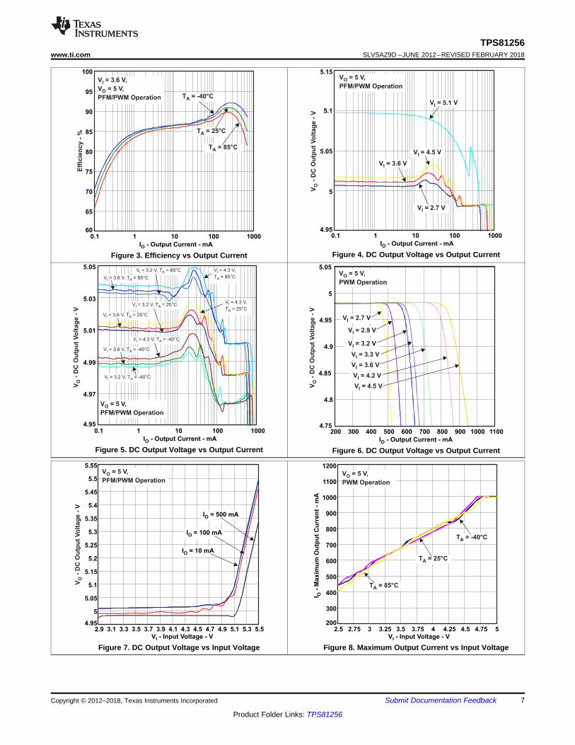
Figure 3. Efficiency vs Output Current Figure 4. DC Output Voltage vs Output Current
Figure 5. DC Output Voltage vs Output Current Figure 6. DC Output Voltage vs Output Current
Figure 7. DC Output Voltage vs Input Voltage Figure 8. Maximum Output Current vs Input Voltage

0 100 200 300 400 500 600 700 800 900 1000
V = 5 V,
PFM/PWM OperationO
0
0.1
0.2
0.3
0.4
0.5
0.6
0.7
0.8
0.9
1
1.1
1.2
1.3
I-
Inp
ut
Cu
rren
t -
mA
IN
V = 2.6 VI
V = 4.5 VI
V = 3.6 VI
V = 3.3 VI
V = 3 VI
V = 4.2 VI
0
5
10
15
20
25
30
35
40
45
50
0 100 200 300 400 500 600 700
V-
Peak-t
o-P
eak O
utp
ut
Rip
ple
Vo
ltag
e -
mV
O
V = 2.7 VI
V = 4.2 VI
V = 3.6 VIV = 3.3 VI
V = 5 V,
PFM/PWM OperationO
V - Input Voltage - VI
0
5
10
15
20
25
30
35
40
45
50
55
60
65
70
75
2.5 2.7 2.9 3.1 3.3 3.5 3.7 3.9 4.1 4.3 4.5 4.7 4.9
Su
pp
ly C
urr
en
t -
Am
V = 5 V,
I = 0 mAO
O
T = 85°CA
T = 25°CA
T = -40°CA
8
TPS81256SLVSAZ9D –JUNE 2012–REVISED FEBRUARY 2018 www.ti.com
Product Folder Links: TPS81256
Submit Documentation Feedback Copyright © 2012–2018, Texas Instruments Incorporated
Figure 9. Peak-To-Peak Output Ripple Voltage vs OutputCurrent
Figure 10. Supply Current vs Input Voltage
Figure 11. Input Current vs Output Current

L
GND
EN
VIN
C
2.2µF
I
1µH
C
2.2µF
O
VOUT
DC/DC CONVERTER
UndervoltageLockout
ThermalShutdown
Softstart
ControlLogic
Ga
te D
rive
r PMOS
ValleyCurrentSense
Err
or
Am
plif
ier
VREF
NMOS
Modulator
x2
9
TPS81256www.ti.com SLVSAZ9D –JUNE 2012–REVISED FEBRUARY 2018
Product Folder Links: TPS81256
Submit Documentation FeedbackCopyright © 2012–2018, Texas Instruments Incorporated
8 Detailed Description
8.1 OverviewThe TPS81256 is a stand-alone, synchronous, step-up converter module. The converter operates at a quasi-constant 4-MHz frequency pulse width modulation (PWM) at moderate to heavy load currents. At light loadcurrents, the TPS81256 converter operates in power-save mode with pulse frequency modulation (PFM).
8.2 Functional Block Diagram
8.3 Feature Description
8.3.1 OperationDuring PWM operation, the converter uses a novel quasi-constant on-time valley current mode control scheme toachieve excellent line/load regulation and allows the use of a small ceramic inductor and capacitors. Based onthe VIN/VOUT ratio, a simple circuit predicts the required on-time.
At the beginning of the switching cycle, the low-side N-MOS switch is turned-on and the inductor current rampsup to a peak current that is defined by the on-time and the inductance. In the second phase, once the on-timerhas expired, the rectifier is turned-on and the inductor current decays to a preset valley current threshold. Finally,the switching cycle repeats by setting the on timer again and activating the low-side N-MOS switch.

hg gOUT
OUT(DC) IN(CL)
IN
VI = I
V
10
TPS81256SLVSAZ9D –JUNE 2012–REVISED FEBRUARY 2018 www.ti.com
Product Folder Links: TPS81256
Submit Documentation Feedback Copyright © 2012–2018, Texas Instruments Incorporated
Feature Description (continued)In general, a dc/dc step-up converter can only operate in "true" boost mode, i.e. the output “boosted” by a certainamount above the input voltage. The TPS81256 device operates differently as it can smoothly transition in andout of zero duty cycle operation. Therefore the output can be kept as close as possible to its regulation limitseven though the converter is subject to an input voltage that tends to be excessive. In this operation mode, theoutput current capability of the regulator is limited to ca. 150mA. Refer to the typical characteristics section (DCOutput Voltage vs. Input Voltage) for further details.
The current mode architecture with adaptive slope compensation provides excellent transient load responsewhile requiring only one external tiny capacitor for output filtering and loop stability purposes. Internal soft-startand loop compensation simplifies the application design process.
8.3.2 Power-Save ModeThe TPS81256 integrates a power-save mode to improve efficiency at light load. In power-save mode theconverter only operates when the output voltage trips below a set threshold voltage.
It ramps up the output voltage with several pulses and goes into power save mode when the output voltageexceeds the set threshold voltage.
PFM mode is exited and the PWM mode entered in case the output current can no longer be supported in PFMmode.
Figure 12. Power-Save Example
8.3.3 Current Limit Operation, Maximum Output CurrentThe TPS81256 directly and accurately controls the average input current through intelligent adjustment of thevalley current limit. The current limit circuit employs a valley current sensing scheme. Current limit detectionoccurs during the off-time by sensing of the voltage drop across the synchronous rectifier.
The output voltage is reduced as the power stage of the device operates in a constant current mode. Themaximum continuous output current (IOUT(CL)), before entering current limit (CL) operation, can be defined byEquation 1.
(1)
The output current, IOUT(DC), is the average of the rectifier ripple current waveform. When the load current isincreased such that the lower peak is above the current limit threshold, the off-time is increased to allow thecurrent to decrease to this threshold before the next on-time begins (so called frequency fold-back mechanism).When the current limit is reached the output voltage decreases during further load increase.

11
TPS81256www.ti.com SLVSAZ9D –JUNE 2012–REVISED FEBRUARY 2018
Product Folder Links: TPS81256
Submit Documentation FeedbackCopyright © 2012–2018, Texas Instruments Incorporated
8.4 Device Functional Modes
8.4.1 Softstart, EnableThe TPS81256 device starts operation when EN is set high and starts up with the soft-start sequence. For properoperation, the EN pin must be terminated and must not be left floating.
The TPS81256 device has an internal softstart circuit that limits the inrush current during start-up. The first stepin the start-up cycle is the pre-charge phase. During pre-charge, the rectifying switch is turned on until the outputcapacitor is charged to a value close to the input voltage. The rectifying switch is current limited (approx. 200mA)during this phase. This mechanism is used to limit the output current under short-circuit condition.
Once the output capacitor has been biased to the input voltage, the converter starts switching. The soft-startsystem progressively increases the on-time as a function of the input-to-output voltage ratio. As soon as theoutput voltage is reached, the regulation loop takes control and full current operation is permitted.
Pulling the EN pin low forces the device in shutdown, with a shutdown current of typically 1µA. In this mode, trueload disconnect between the battery and load prevents current flow from VIN to VOUT, as well as reverse flowfrom VOUT to VIN.
8.4.2 Load Disconnect and Reverse Current ProtectionRegular boost converters do not disconnect the load from the input supply and therefore a connected battery willbe discharge during shutdown. The advantage of TPS81256 is that this converter is disconnecting the outputfrom the input of the power supply when it is disabled (so called true shutdown mode). In case of a connectedbattery it prevents it from being discharge during shutdown of the converter.
8.4.3 Undervoltage LockoutThe under voltage lockout circuit prevents the device from malfunctioning at low input voltages and the batteryfrom excessive discharge. It disables the output stage of the converter once the falling VIN trips the under-voltagelockout threshold VUVLO which is typically 2.0V. The device starts operation once the rising VIN trips VUVLOthreshold plus its hysteresis of 100 mV at typically 2.1V.
8.4.4 Thermal RegulationThe TPS81256 device contains a thermal regulation loop that monitors the die temperature during the pre-chargephase. If the die temperature rises to high values of about 110°C, the device automatically reduces the current toprevent the die temperature from increasing further. Once the die temperature drops about 10°C below thethreshold, the device will automatically increase the current to the target value. This function also reduces thecurrent during a short-circuit condition.
8.4.5 Thermal ShutdownAs soon as the junction temperature, TJ, exceeds 140°C (typically) the device goes into thermal shutdown. In thismode, the high-side and low-side MOSFETs are turned-off. When the junction temperature falls below thethermal shutdown minus its hysteresis, the device continuous the operation.
ESR OUT ESRV I R= g
( )-D =
g
g g
OUT OUT IN
OUT
I V VV
C V f
L
VIN
EN
VOUT
GND
L
VIN
VOUT
DC/DC Converter
TPS81256
ENABLE
GND
CEXT
CI
Co
12
TPS81256SLVSAZ9D –JUNE 2012–REVISED FEBRUARY 2018 www.ti.com
Product Folder Links: TPS81256
Submit Documentation Feedback Copyright © 2012–2018, Texas Instruments Incorporated
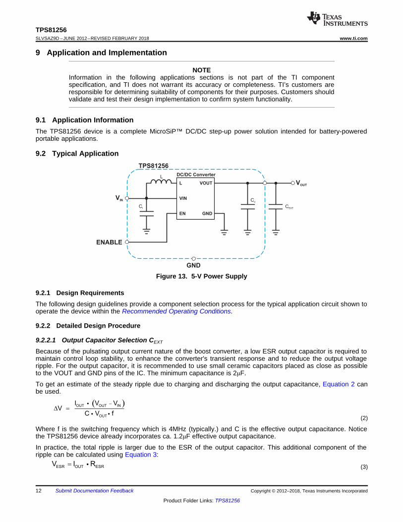
9 Application and Implementation
NOTEInformation in the following applications sections is not part of the TI componentspecification, and TI does not warrant its accuracy or completeness. TI’s customers areresponsible for determining suitability of components for their purposes. Customers shouldvalidate and test their design implementation to confirm system functionality.
9.1 Application InformationThe TPS81256 device is a complete MicroSiP™ DC/DC step-up power solution intended for battery-poweredportable applications.
9.2 Typical Application
Figure 13. 5-V Power Supply
9.2.1 Design RequirementsThe following design guidelines provide a component selection process for the typical application circuit shown tooperate the device within the Recommended Operating Conditions.
9.2.2 Detailed Design Procedure
9.2.2.1 Output Capacitor Selection CEXT
Because of the pulsating output current nature of the boost converter, a low ESR output capacitor is required tomaintain control loop stability, to enhance the converter's transient response and to reduce the output voltageripple. For the output capacitor, it is recommended to use small ceramic capacitors placed as close as possibleto the VOUT and GND pins of the IC. The minimum capacitance is 2μF.
To get an estimate of the steady ripple due to charging and discharging the output capacitance, Equation 2 canbe used.
(2)
Where f is the switching frequency which is 4MHz (typically.) and C is the effective output capacitance. Noticethe TPS81256 device already incorporates ca. 1.2μF effective output capacitance.
In practice, the total ripple is larger due to the ESR of the output capacitor. This additional component of theripple can be calculated using Equation 3:
(3)

13
TPS81256www.ti.com SLVSAZ9D –JUNE 2012–REVISED FEBRUARY 2018
Product Folder Links: TPS81256
Submit Documentation FeedbackCopyright © 2012–2018, Texas Instruments Incorporated
Typical Application (continued)An MLCC capacitor with twice the value of the calculated minimum should be used due to DC bias effects. Theoutput capacitor requires either an X7R or X5R dielectric. Y5V and Z5U dielectric capacitors, aside from theirwide variation in capacitance over temperature, become resistive at high frequencies. There are no additionalrequirements regarding minimum ESR. Larger capacitors cause lower output voltage ripple as well as loweroutput voltage drop during load transients but the total output capacitance value should not exceed ca. 30µF.
DC bias effect: high cap. ceramic capacitors exhibit DC bias effects, which have a strong influence on thedevice's effective capacitance. Therefore the right capacitor value has to be chosen very carefully. Package sizeand voltage rating in combination with material are responsible for differences between the rated capacitor valueand it's effective capacitance. For instance, a 4.7µF X5R 16V 0603 MLCC capacitor would typically show aneffective capacitance of less than 2.5µF (under 5V bias condition, high temperature and ageing effects).
Because the damping factor in the output path is directly related to several resistive parameters (e.g. inductorDCR, power-stage rDS(on), PWB DC resistance, load switches rDS(on) …) that are temperature dependant, theconverter small and large signal behavior must be checked over the input voltage range, load current range andtemperature range.
The easiest sanity test is to evaluate, directly at the converter’s output, the following aspects:
• PFM/PWM efficiency• PFM/PWM and PWM load transient response
During the recovery time from a load transient, the output voltage can be monitored for settling time, overshoot orringing that helps judge the converter’s stability. Without any ringing, the loop has usually more than 45° of phasemargin.
(1) See Third-Party Products Disclaimer
Table 3. Recommended Capacitor CEXT
REFERENCE DESCRIPTION PART NUMBER, MANUFACTURER (1)
CEXT 4.7μF, 16V, 0603, X5R ceramic GRM188R61C475KAAJ, muRata
9.2.2.2 Input Capacitor SelectionIn a dc/dc boost converter, since the input current is continuous, only minimum input capacitance is required. TheTPS81256 device integrates a low ESR decoupling capacitor to prevent large voltage transients that can causemisbehavior of the device or interference in other circuits in the system.
For most applications, the input capacitor that is integrated into the TPS81256 should be sufficient. If theapplication exhibits a noisy or erratic switching frequency, experiment with additional input capacitance to find aremedy. Multilayer ceramic capacitors are an excellent choice for input decoupling of the step-up converter asthey have extremely low ESR and are available in small footprints. Additional input capacitors should be locatedas close as possible to the device.
The TPS81256 uses a tiny ceramic input capacitor. When a ceramic capacitor is combined with trace or cableinductance, such as from a wall adapter, a load step at the output can induce ringing at the VIN pin. This ringingcan couple to the output and be mistaken as loop instability or can even damage the part. In this circumstance,additional "bulk" capacitance, such as electrolytic or tantalum, should be placed between the input of theconverter and the power source lead to reduce ringing that can occur between the inductance of the powersource leads and CI.
V = 2.7 V,
V = 5.0 VI
O
40 to 400 mA Load Step
V = 4.5 V,
V = 5.0 VI
O
40 to 400 mA Load Step
0 to 500mA Load Sweep
V = 3.6 V,
V = 5.0 VI
O
V = 3.6 V,
V = 5.0 VI
O
40 to 400 mA Load Step
V = 5.0 V,
IO
O = 0 mA
V = 2.7 VI
V = 3.6 VI
V = 4.5 VI
V = 3.6 V,
V = 5.0 VI
O
Load Sweep, up to 830mA
670mA830mA
14
TPS81256SLVSAZ9D –JUNE 2012–REVISED FEBRUARY 2018 www.ti.com
Product Folder Links: TPS81256
Submit Documentation Feedback Copyright © 2012–2018, Texas Instruments Incorporated
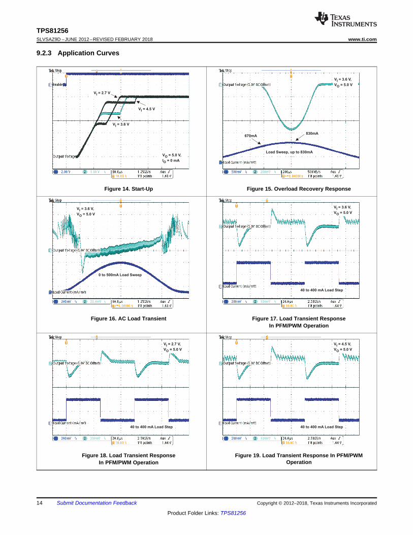
9.2.3 Application Curves
Figure 14. Start-Up Figure 15. Overload Recovery Response
Figure 16. AC Load Transient Figure 17. Load Transient ResponseIn PFM/PWM Operation
Figure 18. Load Transient ResponseIn PFM/PWM Operation
Figure 19. Load Transient Response In PFM/PWMOperation

5.0 V, up to 550mA
EN APA
CLASS-D APA
Audio Input
Audio Input
4.7µF
CI
CO
L
VIN
EN
VOUT
GND
L
VIN
3.3 V .. 4.8 V
DC/DC Converter
TPS81256SIP
EN DC/DC
GND
The capacitor is not only required to decouple the audio power amplifier,but is also required to stable operation of the SMPS converter.The SMPS converter should be located in the close vicinity of the audio power amplifier.
(1)
CDECOUPLING
(1)
3.2V to 3.8V Line Step
V = 5.0 VO
40mA to 400mALoad Step
15
TPS81256www.ti.com SLVSAZ9D –JUNE 2012–REVISED FEBRUARY 2018
Product Folder Links: TPS81256
Submit Documentation FeedbackCopyright © 2012–2018, Texas Instruments Incorporated
Figure 20. Combined Line/Load Transient Response
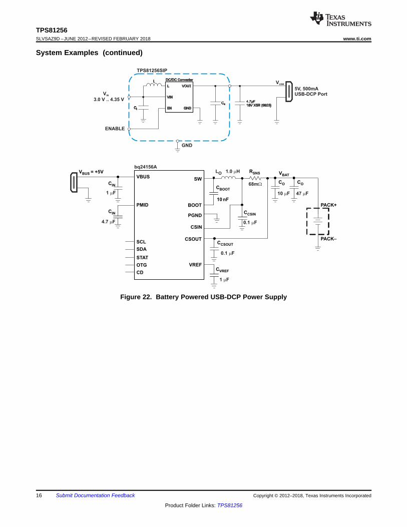
9.3 System Examples
Figure 21. "Boosted" Audio Power Supply
CVREF
10 nF
CBOOT
PACK–
PACK+
CCSOUTSCL
SDA
CSOUT
CSIN
PGND
SW
STAT
VREF
PMID
VBUSVBUS = +5V
CIN
BOOT
OTG
CD
RSNS
CCSIN
VBAT
1 Fm
4.7 Fm
L 1.0 HO m
CO
10 Fm
0.1 Fm
0.1 Fm
1 Fm
bq24156A
68mW
47 Fm
COCIN
CI
CO
VIN
3.0 V .. 4.35 V
TPS81256SIP
ENABLE
GND
L
VIN
EN
VOUT
GND
L DC/DC Converter
4.7µF16V X5R (0603)
5V, 500mAUSB-DCP Port
VUSB
16
TPS81256SLVSAZ9D –JUNE 2012–REVISED FEBRUARY 2018 www.ti.com
Product Folder Links: TPS81256
Submit Documentation Feedback Copyright © 2012–2018, Texas Instruments Incorporated
System Examples (continued)
Figure 22. Battery Powered USB-DCP Power Supply
Copper Trace Width
Solder Pad Width
Solder Mask Opening
Copper Trace ThicknessSolder Mask Thickness
M0200-01
17
TPS81256www.ti.com SLVSAZ9D –JUNE 2012–REVISED FEBRUARY 2018
Product Folder Links: TPS81256
Submit Documentation FeedbackCopyright © 2012–2018, Texas Instruments Incorporated
10 Power Supply RecommendationsThe TPS81256 has no special requirements for its input power supply. The input power supply's output currentneeds to be rated according to the supply voltage, output voltage and output current of the TPS81256
(1) Circuit traces from non-solder-mask defined PWB lands should be 75μm to 100μm wide in the exposed area inside the solder maskopening. Wider trace widths reduce device stand off and affect reliability.
(2) Best reliability results are achieved when the PWB laminate glass transition temperature is above the operating the range of theintended application.
(3) Recommend solder paste is Type 3 or Type 4.(4) For a PWB using a Ni/Au surface finish, the gold thickness should be less than 0.5mm to avoid a reduction in thermal fatigue
performance.(5) Solder mask thickness should be less than 20 μm on top of the copper circuit pattern.(6) For best solder stencil performance use laser cut stencils with electro polishing. Chemically etched stencils give inferior solder paste
volume control.
11 Layout
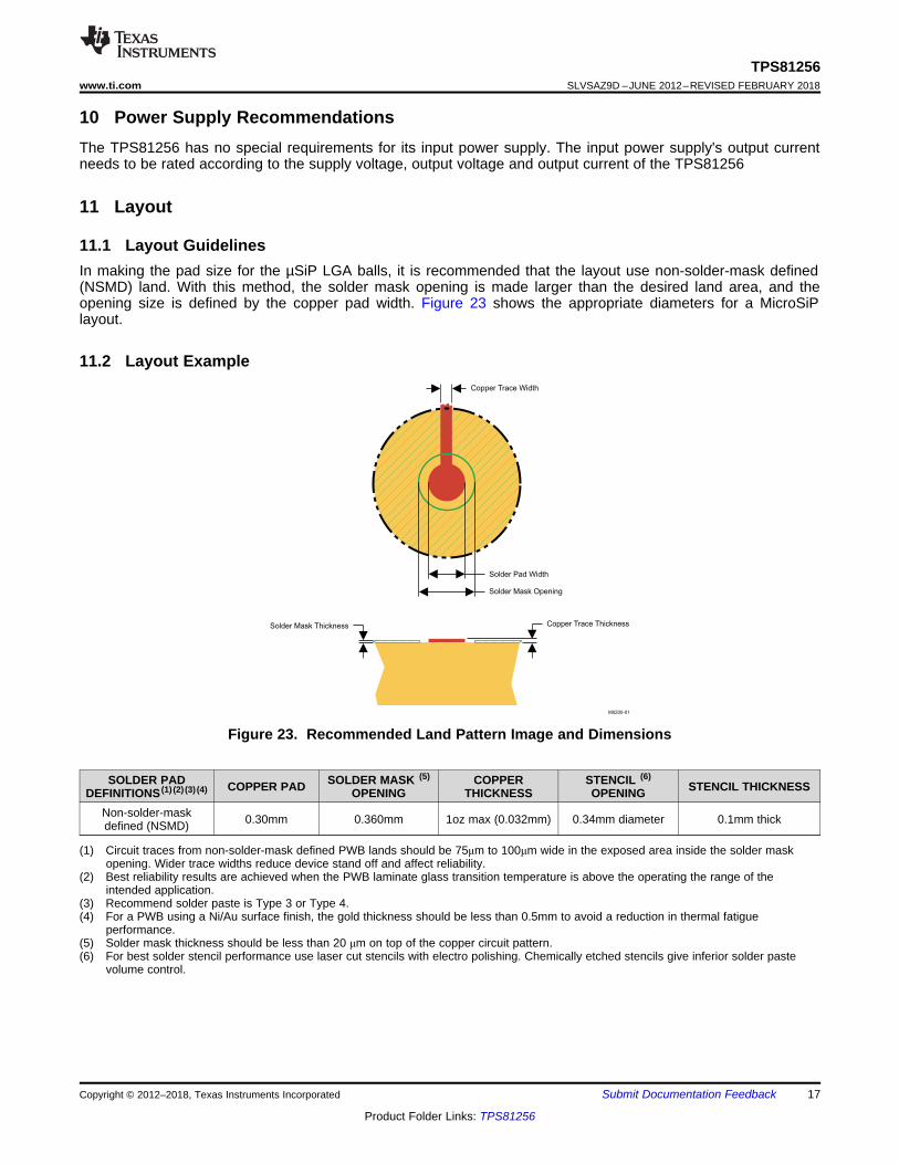
11.1 Layout GuidelinesIn making the pad size for the µSiP LGA balls, it is recommended that the layout use non-solder-mask defined(NSMD) land. With this method, the solder mask opening is made larger than the desired land area, and theopening size is defined by the copper pad width. Figure 23 shows the appropriate diameters for a MicroSiPlayout.
11.2 Layout Example
Figure 23. Recommended Land Pattern Image and Dimensions
SOLDER PADDEFINITIONS (1) (2) (3) (4) COPPER PAD SOLDER MASK (5)
OPENINGCOPPER
THICKNESSSTENCIL (6)
OPENING STENCIL THICKNESS
Non-solder-maskdefined (NSMD) 0.30mm 0.360mm 1oz max (0.032mm) 0.34mm diameter 0.1mm thick
18
TPS81256SLVSAZ9D –JUNE 2012–REVISED FEBRUARY 2018 www.ti.com
Product Folder Links: TPS81256
Submit Documentation Feedback Copyright © 2012–2018, Texas Instruments Incorporated
11.3 Surface Mount InformationThe TPS81256 MicroSiP DC/DC converter uses an open frame construction that is designed for a fullyautomated assembly process and that features a large surface area for pick and place operations. See the "PickArea" in the package drawings.
Package height and weight have been kept to a minimum thereby to allow the MicroSiP device to be handledsimilarly to a 0805 component.
See JEDEC/IPC standard J-STD-20b for reflow recommendations.
11.4 Thermal and Reliability InformationThe TPS81256 output current may need to be de-rated if it is required to operate in a high ambient temperatureor deliver a large amount of continuous power. The amount of current de-rating is dependent upon the inputvoltage, output power and environmental thermal conditions. Care should especially be taken in applicationswhere the localized PWB temperature exceeds 65°C.
The TPS81256 die and inductor temperature should be kept lower than the maximum rating of 125°C, so careshould be taken in the circuit layout to ensure good heat sinking. Sufficient cooling should be provided to ensurereliable operation.
To estimate the junction temperature, approximate the power dissipation within the TPS81256 by applying thetypical efficiency stated in this datasheet to the desired output power; or, by taking a power measurement if youhave an actual TPS81256 device or a TPS81256EVM evaluation module. Then calculate the internaltemperature rise of the TPS81256 above the surface of the printed circuit board by multiplying the TPS81256power dissipation by the thermal resistance.
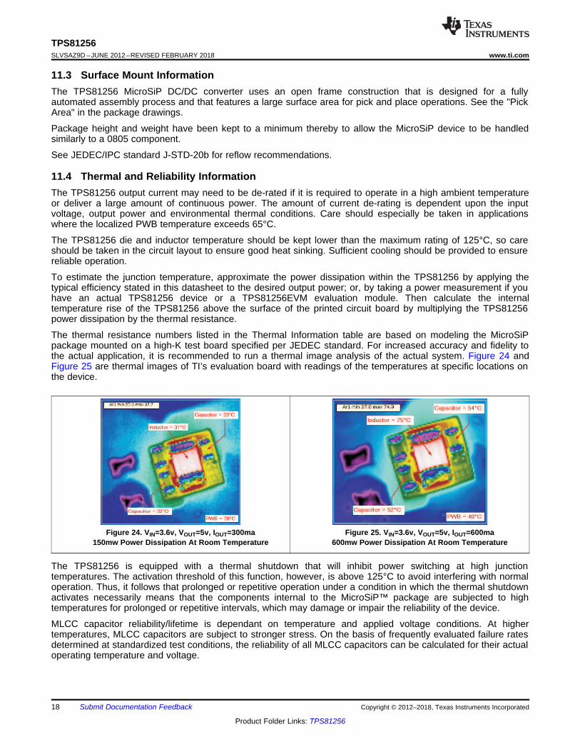
The thermal resistance numbers listed in the Thermal Information table are based on modeling the MicroSiPpackage mounted on a high-K test board specified per JEDEC standard. For increased accuracy and fidelity tothe actual application, it is recommended to run a thermal image analysis of the actual system. Figure 24 andFigure 25 are thermal images of TI’s evaluation board with readings of the temperatures at specific locations onthe device.
Figure 24. VIN=3.6v, VOUT=5v, IOUT=300ma150mw Power Dissipation At Room Temperature
Figure 25. VIN=3.6v, VOUT=5v, IOUT=600ma600mw Power Dissipation At Room Temperature
The TPS81256 is equipped with a thermal shutdown that will inhibit power switching at high junctiontemperatures. The activation threshold of this function, however, is above 125°C to avoid interfering with normaloperation. Thus, it follows that prolonged or repetitive operation under a condition in which the thermal shutdownactivates necessarily means that the components internal to the MicroSiP™ package are subjected to hightemperatures for prolonged or repetitive intervals, which may damage or impair the reliability of the device.
MLCC capacitor reliability/lifetime is dependant on temperature and applied voltage conditions. At highertemperatures, MLCC capacitors are subject to stronger stress. On the basis of frequently evaluated failure ratesdetermined at standardized test conditions, the reliability of all MLCC capacitors can be calculated for their actualoperating temperature and voltage.

0.01
0.1
1
10
100
1000
10000
20 40 60 80 100 120 140Capacitor Case Temperature ( °C)
Tim
e (T
hous
and
Hou
rs)
VBias=5VVBias=4.35VVBias=3.6VVBias=3V
G000
19
TPS81256www.ti.com SLVSAZ9D –JUNE 2012–REVISED FEBRUARY 2018
Product Folder Links: TPS81256
Submit Documentation FeedbackCopyright © 2012–2018, Texas Instruments Incorporated
Thermal and Reliability Information (continued)
Figure 26. Capacitor Lifetime vs Capacitor Case Temperature
Failures caused by systematic degradation can be described by the Arrhenius model. The most criticalparameter (IR) is the Insulation Resistance (i.e. leakage current). The drop of IR below a lower limit (e.g. 1 MΩ)is used as the failure criterion, see Figure 26. It should be noted that the wear-out mechanisms occurring in theMLCC capacitors are not reversible but cumulative over time.
20
TPS81256SLVSAZ9D –JUNE 2012–REVISED FEBRUARY 2018 www.ti.com
Product Folder Links: TPS81256
Submit Documentation Feedback Copyright © 2012–2018, Texas Instruments Incorporated
12 Device and Documentation Support
12.1 Device Support
12.1.1 Third-Party Products DisclaimerTI'S PUBLICATION OF INFORMATION REGARDING THIRD-PARTY PRODUCTS OR SERVICES DOES NOTCONSTITUTE AN ENDORSEMENT REGARDING THE SUITABILITY OF SUCH PRODUCTS OR SERVICESOR A WARRANTY, REPRESENTATION OR ENDORSEMENT OF SUCH PRODUCTS OR SERVICES, EITHERALONE OR IN COMBINATION WITH ANY TI PRODUCT OR SERVICE.
12.2 Community ResourcesThe following links connect to TI community resources. Linked contents are provided "AS IS" by the respectivecontributors. They do not constitute TI specifications and do not necessarily reflect TI's views; see TI's Terms ofUse.
TI E2E™ Online Community TI's Engineer-to-Engineer (E2E) Community. Created to foster collaborationamong engineers. At e2e.ti.com, you can ask questions, share knowledge, explore ideas and helpsolve problems with fellow engineers.
Design Support TI's Design Support Quickly find helpful E2E forums along with design support tools andcontact information for technical support.
12.3 TrademarksMicroSiP, E2E are trademarks of Texas Instruments.All other trademarks are the property of their respective owners.
12.4 Electrostatic Discharge CautionThese devices have limited built-in ESD protection. The leads should be shorted together or the device placed in conductive foamduring storage or handling to prevent electrostatic damage to the MOS gates.
12.5 GlossarySLYZ022 — TI Glossary.
This glossary lists and explains terms, acronyms, and definitions.
B1
B2
B3
A1
A2D
E
A3
C1
C3
TOP VIEW BOTTOM VIEW
C2
YM
L
LS
B
CC
21
TPS81256www.ti.com SLVSAZ9D –JUNE 2012–REVISED FEBRUARY 2018
Product Folder Links: TPS81256
Submit Documentation FeedbackCopyright © 2012–2018, Texas Instruments Incorporated
13 Mechanical, Packaging, and Orderable InformationThe following pages include mechanical, packaging, and orderable information. This information is the mostcurrent data available for the designated devices. This data is subject to change without notice and revision ofthis document. For browser-based versions of this data sheet, refer to the left-hand navigation.
MicroSiP DC/DC Module Package DimensionsThe TPS81256 device is available in a 9-bump ball grid array (BGA) package. The package dimensions are:• D = 2.925 ±0.05 mm• E = 2.575 ±0.05 mm
Code:• CC — Package marking Chip Code (see Package Option Addendum for more details)• YML — Y: Year, M: Month, L: Lot trace code• LSB — L: Lot trace code, S: Site code, B: Board locator
Figure 27. µSIP 9-Pin Dimensions and Markings
www.ti.com
PACKAGE OUTLINE
C
B2.9752.875
A
2.6252.525
1 MAX
0.100.06
2 TYP
1 TYP
2
TYP
1
TYP
9X0.350.25
MicroSiP - 1 mm max heightSIP0009AMICRO SYSTEM IN PACKAGE
4218355/A 06/2014
INDEX AREAPIN A1
NOTE 3PICK AREA
0.05 C
SEATING PLANE
0.015 C A B
1 2
A
B
C
3
TM
NOTES:
1. All linear dimensions are in millimeters. Any dimensions in parenthesis are for reference only. Dimensioning and tolerancingper ASME Y14.5M.
2. This drawing is subject to change without notice.3. For pick and place nozzle recommendation, see product datasheet.4. Location, size and quantity of each component are for reference only and may vary.
MicroSiP is a trademark of Texas Instruments.
SCALE 5.500
22
TPS81256SLVSAZ9D –JUNE 2012–REVISED FEBRUARY 2018 www.ti.com
Product Folder Links: TPS81256
Submit Documentation Feedback Copyright © 2012–2018, Texas Instruments Incorporated

www.ti.com
EXAMPLE BOARD LAYOUT
(1) TYP
( )METAL
0.3
SOLDER MASKOPENING
0.05 MAX 0.05 MIN
9X ( )SEE DETAILS
0.3
(1)TYP
METAL UNDER MASK
( )SOLDER MASKOPENING
0.3
MicroSiP - 1 mm max heightSIP0009AMICRO SYSTEM IN PACKAGE
4218355/A 06/2014
SYMM
SYMM
1 3
A
B
C
2
SCALE:20X
NOTES: (continued)
LAND PATTERN EXAMPLE
TM
5. For more information, see Texas Instruments literature number SBVA017 (www.ti.com/lit/sbva017).
NOT TO SCALESOLDER MASK DETAILS
NON-SOLDER MASKDEFINED
(PREFERRED)
SOLDER MASKDEFINED
23
TPS81256www.ti.com SLVSAZ9D –JUNE 2012–REVISED FEBRUARY 2018
Product Folder Links: TPS81256
Submit Documentation FeedbackCopyright © 2012–2018, Texas Instruments Incorporated

www.ti.com
EXAMPLE STENCIL DESIGN
METALUNDER PASTE
( )0.34
(1) TYP
(1)TYP
( ) TYPSEE DETAIL
0.34
MicroSiP - 1 mm max heightSIP0009AMICRO SYSTEM IN PACKAGE
4218355/A 06/2014
TM
NOTES: (continued)
6. Laser cutting apertures with trapezoidal walls and rounded corners may offer better paste release. IPC-7525 may have alternatedesign recommendations.
SYMM
SYMM
1 3
A
B
C
2
BASED ON 0.1 mm THICK STENCILSOLDER PASTE EXAMPLE
SCALE:20X
TYPICALSOLDER PASTE DETAIL
24
TPS81256SLVSAZ9D –JUNE 2012–REVISED FEBRUARY 2018 www.ti.com
Product Folder Links: TPS81256
Submit Documentation Feedback Copyright © 2012–2018, Texas Instruments Incorporated

PACKAGE OPTION ADDENDUM
www.ti.com 2-Feb-2018
Addendum-Page 1
PACKAGING INFORMATION
Orderable Device Status(1)
Package Type PackageDrawing
Pins PackageQty
Eco Plan(2)
Lead/Ball Finish(6)
MSL Peak Temp(3)
Op Temp (°C) Device Marking(4/5)
Samples
TPS81256SIPR ACTIVE uSiP SIP 9 3000 Green (RoHS& no Sb/Br)
Call TI Level-2-260C-1 YEAR -40 to 85 TTTXI256
TPS81256SIPT ACTIVE uSiP SIP 9 250 Green (RoHS& no Sb/Br)
Call TI Level-2-260C-1 YEAR -40 to 85 TTTXI256
(1) The marketing status values are defined as follows:ACTIVE: Product device recommended for new designs.LIFEBUY: TI has announced that the device will be discontinued, and a lifetime-buy period is in effect.NRND: Not recommended for new designs. Device is in production to support existing customers, but TI does not recommend using this part in a new design.PREVIEW: Device has been announced but is not in production. Samples may or may not be available.OBSOLETE: TI has discontinued the production of the device.
(2) RoHS: TI defines "RoHS" to mean semiconductor products that are compliant with the current EU RoHS requirements for all 10 RoHS substances, including the requirement that RoHS substancedo not exceed 0.1% by weight in homogeneous materials. Where designed to be soldered at high temperatures, "RoHS" products are suitable for use in specified lead-free processes. TI mayreference these types of products as "Pb-Free".RoHS Exempt: TI defines "RoHS Exempt" to mean products that contain lead but are compliant with EU RoHS pursuant to a specific EU RoHS exemption.Green: TI defines "Green" to mean the content of Chlorine (Cl) and Bromine (Br) based flame retardants meet JS709B low halogen requirements of <=1000ppm threshold. Antimony trioxide basedflame retardants must also meet the <=1000ppm threshold requirement.
(3) MSL, Peak Temp. - The Moisture Sensitivity Level rating according to the JEDEC industry standard classifications, and peak solder temperature.
(4) There may be additional marking, which relates to the logo, the lot trace code information, or the environmental category on the device.
(5) Multiple Device Markings will be inside parentheses. Only one Device Marking contained in parentheses and separated by a "~" will appear on a device. If a line is indented then it is a continuationof the previous line and the two combined represent the entire Device Marking for that device.
(6) Lead/Ball Finish - Orderable Devices may have multiple material finish options. Finish options are separated by a vertical ruled line. Lead/Ball Finish values may wrap to two lines if the finishvalue exceeds the maximum column width.
Important Information and Disclaimer:The information provided on this page represents TI's knowledge and belief as of the date that it is provided. TI bases its knowledge and belief on informationprovided by third parties, and makes no representation or warranty as to the accuracy of such information. Efforts are underway to better integrate information from third parties. TI has taken andcontinues to take reasonable steps to provide representative and accurate information but may not have conducted destructive testing or chemical analysis on incoming materials and chemicals.TI and TI suppliers consider certain information to be proprietary, and thus CAS numbers and other limited information may not be available for release.
In no event shall TI's liability arising out of such information exceed the total purchase price of the TI part(s) at issue in this document sold by TI to Customer on an annual basis.
PACKAGE OPTION ADDENDUM
www.ti.com 2-Feb-2018
Addendum-Page 2

TAPE AND REEL INFORMATION
*All dimensions are nominal
Device PackageType
PackageDrawing
Pins SPQ ReelDiameter
(mm)
ReelWidth
W1 (mm)
A0(mm)
B0(mm)
K0(mm)
P1(mm)
W(mm)
Pin1Quadrant
TPS81256SIPR uSiP SIP 9 3000 178.0 9.0 2.83 3.18 1.2 4.0 8.0 Q2
PACKAGE MATERIALS INFORMATION
www.ti.com 2-Feb-2018
Pack Materials-Page 1

*All dimensions are nominal
Device Package Type Package Drawing Pins SPQ Length (mm) Width (mm) Height (mm)
TPS81256SIPR uSiP SIP 9 3000 223.0 194.0 35.0
PACKAGE MATERIALS INFORMATION
www.ti.com 2-Feb-2018
Pack Materials-Page 2
IMPORTANT NOTICE
Texas Instruments Incorporated (TI) reserves the right to make corrections, enhancements, improvements and other changes to itssemiconductor products and services per JESD46, latest issue, and to discontinue any product or service per JESD48, latest issue. Buyersshould obtain the latest relevant information before placing orders and should verify that such information is current and complete.TI’s published terms of sale for semiconductor products (http://www.ti.com/sc/docs/stdterms.htm) apply to the sale of packaged integratedcircuit products that TI has qualified and released to market. Additional terms may apply to the use or sale of other types of TI products andservices.Reproduction of significant portions of TI information in TI data sheets is permissible only if reproduction is without alteration and isaccompanied by all associated warranties, conditions, limitations, and notices. TI is not responsible or liable for such reproduceddocumentation. Information of third parties may be subject to additional restrictions. Resale of TI products or services with statementsdifferent from or beyond the parameters stated by TI for that product or service voids all express and any implied warranties for theassociated TI product or service and is an unfair and deceptive business practice. TI is not responsible or liable for any such statements.Buyers and others who are developing systems that incorporate TI products (collectively, “Designers”) understand and agree that Designersremain responsible for using their independent analysis, evaluation and judgment in designing their applications and that Designers havefull and exclusive responsibility to assure the safety of Designers' applications and compliance of their applications (and of all TI productsused in or for Designers’ applications) with all applicable regulations, laws and other applicable requirements. Designer represents that, withrespect to their applications, Designer has all the necessary expertise to create and implement safeguards that (1) anticipate dangerousconsequences of failures, (2) monitor failures and their consequences, and (3) lessen the likelihood of failures that might cause harm andtake appropriate actions. Designer agrees that prior to using or distributing any applications that include TI products, Designer willthoroughly test such applications and the functionality of such TI products as used in such applications.TI’s provision of technical, application or other design advice, quality characterization, reliability data or other services or information,including, but not limited to, reference designs and materials relating to evaluation modules, (collectively, “TI Resources”) are intended toassist designers who are developing applications that incorporate TI products; by downloading, accessing or using TI Resources in anyway, Designer (individually or, if Designer is acting on behalf of a company, Designer’s company) agrees to use any particular TI Resourcesolely for this purpose and subject to the terms of this Notice.TI’s provision of TI Resources does not expand or otherwise alter TI’s applicable published warranties or warranty disclaimers for TIproducts, and no additional obligations or liabilities arise from TI providing such TI Resources. TI reserves the right to make corrections,enhancements, improvements and other changes to its TI Resources. TI has not conducted any testing other than that specificallydescribed in the published documentation for a particular TI Resource.Designer is authorized to use, copy and modify any individual TI Resource only in connection with the development of applications thatinclude the TI product(s) identified in such TI Resource. NO OTHER LICENSE, EXPRESS OR IMPLIED, BY ESTOPPEL OR OTHERWISETO ANY OTHER TI INTELLECTUAL PROPERTY RIGHT, AND NO LICENSE TO ANY TECHNOLOGY OR INTELLECTUAL PROPERTYRIGHT OF TI OR ANY THIRD PARTY IS GRANTED HEREIN, including but not limited to any patent right, copyright, mask work right, orother intellectual property right relating to any combination, machine, or process in which TI products or services are used. Informationregarding or referencing third-party products or services does not constitute a license to use such products or services, or a warranty orendorsement thereof. Use of TI Resources may require a license from a third party under the patents or other intellectual property of thethird party, or a license from TI under the patents or other intellectual property of TI.TI RESOURCES ARE PROVIDED “AS IS” AND WITH ALL FAULTS. TI DISCLAIMS ALL OTHER WARRANTIES ORREPRESENTATIONS, EXPRESS OR IMPLIED, REGARDING RESOURCES OR USE THEREOF, INCLUDING BUT NOT LIMITED TOACCURACY OR COMPLETENESS, TITLE, ANY EPIDEMIC FAILURE WARRANTY AND ANY IMPLIED WARRANTIES OFMERCHANTABILITY, FITNESS FOR A PARTICULAR PURPOSE, AND NON-INFRINGEMENT OF ANY THIRD PARTY INTELLECTUALPROPERTY RIGHTS. TI SHALL NOT BE LIABLE FOR AND SHALL NOT DEFEND OR INDEMNIFY DESIGNER AGAINST ANY CLAIM,INCLUDING BUT NOT LIMITED TO ANY INFRINGEMENT CLAIM THAT RELATES TO OR IS BASED ON ANY COMBINATION OFPRODUCTS EVEN IF DESCRIBED IN TI RESOURCES OR OTHERWISE. IN NO EVENT SHALL TI BE LIABLE FOR ANY ACTUAL,DIRECT, SPECIAL, COLLATERAL, INDIRECT, PUNITIVE, INCIDENTAL, CONSEQUENTIAL OR EXEMPLARY DAMAGES INCONNECTION WITH OR ARISING OUT OF TI RESOURCES OR USE THEREOF, AND REGARDLESS OF WHETHER TI HAS BEENADVISED OF THE POSSIBILITY OF SUCH DAMAGES.Unless TI has explicitly designated an individual product as meeting the requirements of a particular industry standard (e.g., ISO/TS 16949and ISO 26262), TI is not responsible for any failure to meet such industry standard requirements.Where TI specifically promotes products as facilitating functional safety or as compliant with industry functional safety standards, suchproducts are intended to help enable customers to design and create their own applications that meet applicable functional safety standardsand requirements. Using products in an application does not by itself establish any safety features in the application. Designers mustensure compliance with safety-related requirements and standards applicable to their applications. Designer may not use any TI products inlife-critical medical equipment unless authorized officers of the parties have executed a special contract specifically governing such use.Life-critical medical equipment is medical equipment where failure of such equipment would cause serious bodily injury or death (e.g., lifesupport, pacemakers, defibrillators, heart pumps, neurostimulators, and implantables). Such equipment includes, without limitation, allmedical devices identified by the U.S. Food and Drug Administration as Class III devices and equivalent classifications outside the U.S.TI may expressly designate certain products as completing a particular qualification (e.g., Q100, Military Grade, or Enhanced Product).Designers agree that it has the necessary expertise to select the product with the appropriate qualification designation for their applicationsand that proper product selection is at Designers’ own risk. Designers are solely responsible for compliance with all legal and regulatoryrequirements in connection with such selection.Designer will fully indemnify TI and its representatives against any damages, costs, losses, and/or liabilities arising out of Designer’s non-compliance with the terms and provisions of this Notice.
Mailing Address: Texas Instruments, Post Office Box 655303, Dallas, Texas 75265Copyright © 2018, Texas Instruments Incorporated


![Torque Converter Voith Torque Converter[1]](https://img.pdfslide.net/doc/110x75/55cf992e550346d0339c0bc5/torque-converter-voith-torque-converter1.jpg)