Embed Size (px)
Citation preview
3.0A, 150Khz, Step-Down Switching Regulator
FEATURES
3.3V, 5.0V, 12V, 15V, and Adjustable Output Versions
Adjustable Version Output Voltage Range, 1.23 to 37V
+/- 4%. Maximum Over Line and Load Conditions
Guaranteed 3.0A Output Current
Wide Input Voltage Range
Requires Only 4 External Components
150Khz Fixed Frequency Internal Oscillator
TTL Shutdown Capability, Low Power Standby Mode
High Efficiency
Uses Readily Available Standard Inductors
Thermal Shutdown and Current Limit Protection
Moisture Sensitivity Level(MSL) Equals1
Applications
Simple High-Efficiency Step-Down(Buck) Regulator
Efficient Pre-Regulator for Linear Regulators
On-Card Switching Regulators
Positive to Negative Converter(Buck-Boost)
Negative Step-Up Converters
Power Supply for Battery Chargers
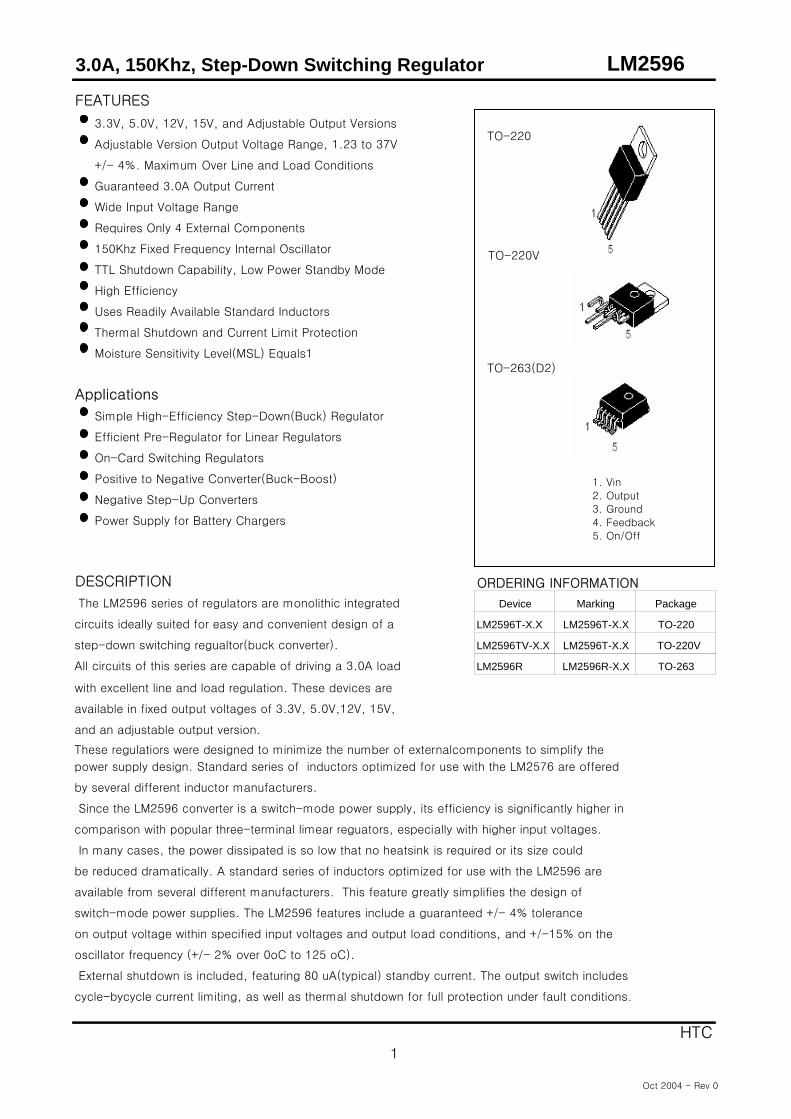
DESCRIPTION ORDERING INFORMATION
The LM2596 series of regulators are monolithic integrated
circuits ideally suited for easy and convenient design of a
step-down switching regualtor(buck converter).
All circuits of this series are capable of driving a 3.0A load
with excellent line and load regulation. These devices are
available in fixed output voltages of 3.3V, 5.0V,12V, 15V,
and an adjustable output version.
These regulatiors were designed to minimize the number of externalcomponents to simplify the
power supply design. Standard series of inductors optimized for use with the LM2576 are offered
by several different inductor manufacturers.
Since the LM2596 converter is a switch-mode power supply, its efficiency is significantly higher in
comparison with popular three-terminal limear reguators, especially with higher input voltages.
available from several different manufacturers. This feature greatly simplifies the design of
switch-mode power supplies. The LM2596 features include a guaranteed +/- 4% tolerance
on output voltage within specified input voltages and output load conditions, and +/-15% on the
oscillator frequency (+/- 2% over 0oC to 125 oC).
External shutdown is included, featuring 80 uA(typical) standby current. The output switch includes
cycle-bycycle current limiting, as well as thermal shutdown for full protection under fault conditions.
TO-220V
HTC
1
LM2596
In many cases, the power dissipated is so low that no heatsink is required or its size could
be reduced dramatically. A standard series of inductors optimized for use with the LM2596 are
LM2596TV-X.X LM2596T-X.X
Device Marking Package
LM2596T-X.X LM2596T-X.X TO-220
LM2596R LM2596R-X.X TO-263
TO-220V
TO-220
1. Vin2. Output3. Ground4. Feedback5. On/Off
TO-263(D2)
Oct 2004 - Rev 0
3.0A, 15V, Step-Down Switching Regulator
HTC
2
LM2596
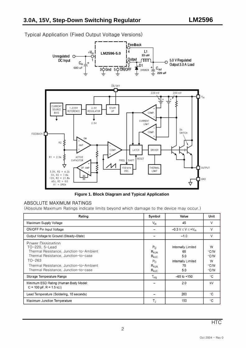
Figure 1. Block Diagram and Typical Application
ABSOLUTE MAXIMUM RATINGS(Absolute Maximum Ratings indicate limits beyond which damage to the device may occur.)
TO-220, 5-Lead
TO-263
Thermal Resistance, Junction-to-AmbientThermal Resistance, Junction-to-case
Thermal Resistance, Junction-to-AmbientThermal Resistance, Junction-to-case
Power Dissipation
Typical Application (Fixed Output Voltage Versions)
680 uF
220 uF1N5824
33 uHLM2596-5.0
Oct 2004 - Rev 0
3.0A, 15V, Step-Down Switching Regulator
HTC
3
LM2596OPERATING RATINGS (Operating Ratings indicate conditions for which the device is intended to befunctional, but do not guarantee specific performance limits. For guaranteed specifications and testconditions, see the Electrical Characteristics.)
ELECTRICAL CHARACTERISTICS / SYSTEM PARAMETERS ([Note 1] Test Circuit Figure 2)(Unless otherwise specified, Vin = 12 V for the 3.3 V, 5.0 V, and Adjustable version, Vin = 25 V forthe 12 V version, and Vin = 30 V for the 15 V version. ILoad = 500 mA. For typical values TJ = 25°C,for min/max values TJ is the operating junction temperature range that applies [Note 2], unlessotherwise noted.)
73
80
90
98
LM2596-3.3 ([ Note 1]. Test Circuit Figure 2 )
73
LM2596-5.0 ([ Note 1]. Test Circuit Figure 1 )
LM2596-ADJ ([ Note 1]. Test Circuit Figure 2 )
LM2596-15 ([ Note 1]. Test Circuit Figure 2 )
LM2596-12 ([ Note 1]. Test Circuit Figure 2 )
LM2596-5.0 ([ Note 1]. Test Circuit Figure 2 )
Oct 2004 - Rev 0
3.0A, 15V, Step-Down Switching Regulator LM2596
HTC
4
ELECTRICAL CHARACTERISTICS / Device Parameters(Unless otherwise specified, Vin = 12 V for the 3.3 V, 5.0 V, and Adjustable version, Vin = 25 V for the 12V version, and Vin = 30 V for the 15 V version. ILoad = 500 mA. For typical values Tj = 25°C, for min/maxvalues Tj is the operating junction temperature range that applies [Note 2], unless otherwise noted.)
1. External components such as the catch diode, inductor, input and output capacitors can affect switching regulator system performance. When the LM2596 is used as shown in the Figure 1 test circuit, system performance will be as shown in system parameters section .2. Tested junction temperature range for the LM2596 : TLOW = –0°C THIGH = +125°C3. The oscillator frequency reduces to approximately 18 kHz in the event of an output short or an overload which causes the regulated output voltage to drop approximately 40% from the nominal output voltage. This self protection feature lowers the average dissipation of the IC by lowering the minimum duty cycle from 5% down to approximately 2%.4. Output (Pin 2) sourcing current. No diode, inductor or capacitor connected to output pin.5. Feedback (Pin 4) removed from output and connected to 0 V.6. Feedback (Pin 4) removed from output and connected to +12 V for the Adjustable, 3.3 V, and 5.0V ersions, and +25 V for the 12 V and15 V versions, to force the output transistor “off”.7. Vin = 40 V.
2
2
10 500
150 173
100
127110
1.161.5
4.53.6
100
173
-
1.40
0
0
0
0
0
3.46.97.5
- 502 30
-10
5
250
0.6
-
2.0-
1.3 0.6
1.3-
5 15
2.0
0.02 5.0V LOGIC = 2.5V (Regulator OFF)V LOGIC = 0.5V (Regulator ON)
Oct 2004 - Rev 0
3.0A, 15V, Step-Down Switching Regulator LM2596
HTC
5
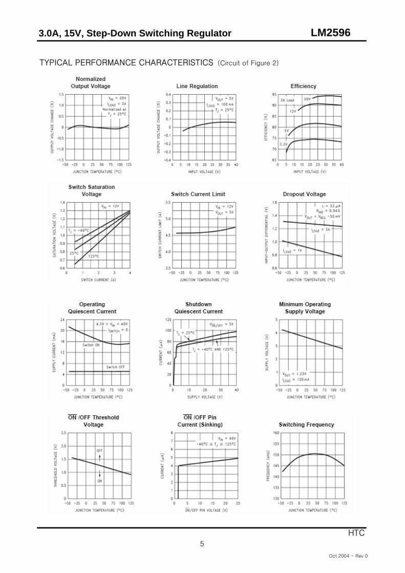
TYPICAL PERFORMANCE CHARACTERISTICS (Circuit of Figure 2)
Oct 2004 - Rev 0

3.0A, 15V, Step-Down Switching Regulator
6
LM2596
HTC
TYPICAL PERFORMANCE CHARACTERISTICS (Circuit of Figure 2)
Feedback Pin Bias Current
Oct 2004 - Rev 0
3.0A, 15V, Step-Down Switching Regulator
7
LM2596
HTC
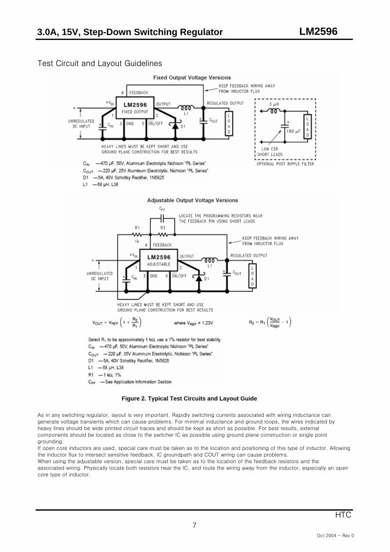
Test Circuit and Layout Guidelines
As in any switching regulator, layout is very important. Rapidly switching currents associated with wiring inductance cangenerate voltage transients which can cause problems. For minimal inductance and ground loops, the wires indicated byheavy lines should be wide printed circuit traces and should be kept as short as possible. For best results, externalcomponents should be located as close to the switcher lC as possible using ground plane construction or single pointgrounding.If open core inductors are used, special care must be taken as to the location and positioning of this type of inductor. Allowingthe inductor flux to intersect sensitive feedback, lC groundpath and COUT wiring can cause problems.When using the adjustable version, special care must be taken as to the location of the feedback resistors and theassociated wiring. Physically locate both resistors near the IC, and route the wiring away from the inductor, especially an opencore type of inductor.
Figure 2. Typical Test Circuits and Layout Guide
Oct 2004 - Rev 0
3.0A, 15V, Step-Down Switching Regulator
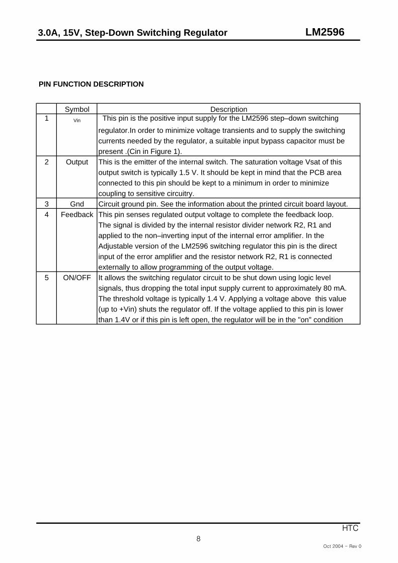
This pin is the positive input supply for the LM2596 step–down switching regulator.In order to minimize voltage transients and to supply the switching currents needed by the regulator, a suitable input bypass capacitor must be present .(Cin in Figure 1).This is the emitter of the internal switch. The saturation voltage Vsat of this output switch is typically 1.5 V. It should be kept in mind that the PCB area connected to this pin should be kept to a minimum in order to minimize coupling to sensitive circuitry.Circuit ground pin. See the information about the printed circuit board layout.This pin senses regulated output voltage to complete the feedback loop. The signal is divided by the internal resistor divider network R2, R1 and applied to the non–inverting input of the internal error amplifier. In the Adjustable version of the LM2596 switching regulator this pin is the direct input of the error amplifier and the resistor network R2, R1 is connected externally to allow programming of the output voltage.It allows the switching regulator circuit to be shut down using logic level signals, thus dropping the total input supply current to approximately 80 mA.The threshold voltage is typically 1.4 V. Applying a voltage above this value(up to +Vin) shuts the regulator off. If the voltage applied to this pin is lowerthan 1.4V or if this pin is left open, the regulator will be in the "on" condition
4
5 ON/OFF
3
Description
Feedback
LM2596
HTC
8
Symbol1 Vin
Output2
Gnd
PIN FUNCTION DESCRIPTION
Oct 2004 - Rev 0
3.0A, 15V, Step-Down Switching Regulator LM2596
HTC
9
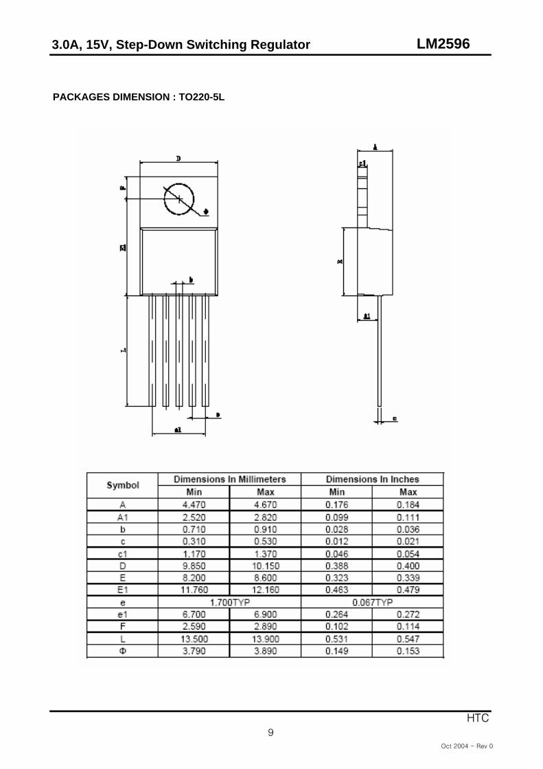
PACKAGES DIMENSION : TO220-5L
Oct 2004 - Rev 0
3.0A, 15V, Step-Down Switching Regulator LM2596
HTC
10
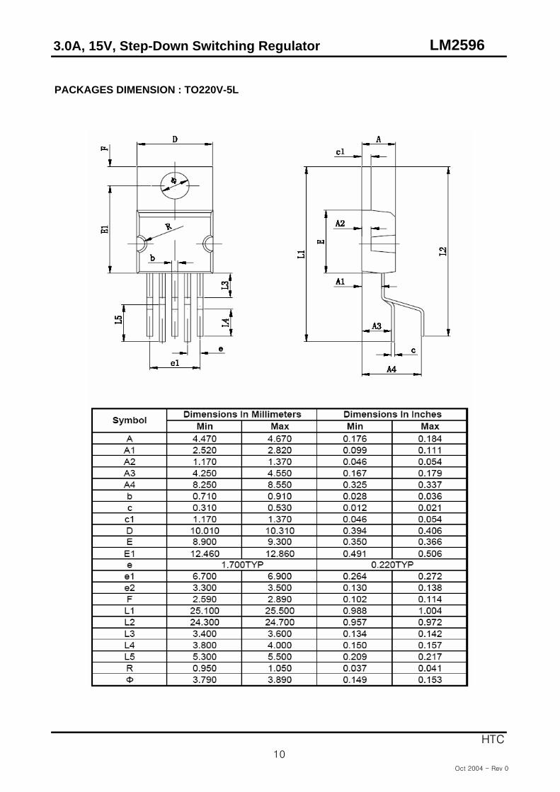
PACKAGES DIMENSION : TO220V-5L
Oct 2004 - Rev 0

3.0A, 15V, Step-Down Switching Regulator
11
LM2596
HTC
PACKAGES DIMENSION : TO263-5L
Oct 2004 - Rev 0