Embed Size (px)
Citation preview

3.1. Introduction to All-Digital PLL
Deog-Kyoon Jeong
Integrated Systems Design Laboratory
Seoul National University

Integrated Systems Design Laboratory, SNU D.K.Jeong
Outline
• Introduction
• ADPLL Building Blocks
– Digital Loop Filter
– Digitally Controlled Oscillator
– Time-to-Digital Converter
• Modeling and Analysis
• Phase Noise
• Summary
2
Integrated Systems Design Laboratory, SNU D.K.Jeong
What is an ADPLL?
• In a broad sense
– ADPLL consists of digital components and
digital equivalents
– Building blocks have input/output levels are
defined in digital domain
• In a strict sense
– A PLL exclusively built from digital function
blocks and contains no passive component
– All components are synthesizable
(Cell-based ADPLL)
3

Integrated Systems Design Laboratory, SNU D.K.Jeong
Classification of PLL Types
• Analog PLL
– Analog PD (multiplier), LF built from passive or
active RC filter, VCO
• Digital PLL
– Digital PD, charge-pump PLL
• All-Digital PLL
– Built from digital function blocks
– All components provide digital interfaces only
[1] R. E. Best 2003
4

Integrated Systems Design Laboratory, SNU D.K.Jeong
ADPLL Block Diagram
• Digital loop filter
• Time-to-digital converter (TDC)
– Linear
– Bang-bang
• Digitally controlled oscillator (DCO)
– Explicit DAC + VCO
– Embedded DAC
TDC DLF DCO
/N
5

Integrated Systems Design Laboratory, SNU D.K.Jeong
Advantages of ADPLL
• No analog tuning voltage
– Suitable for deep-submicron tech using low supply voltage
• PVT variation can be compensated more easily
– Stable transfer characteristic
• Digital filter
– Passive components are not necessary
– Less sensitive to gate leakage
– Easily benefit from technology shrink
– Small area cost reduction
• Information can be processed more flexibly
– More portability and testability
– Most function blocks are synthesizable
6

Integrated Systems Design Laboratory, SNU D.K.Jeong
Advantages of Digital Loop Filter
• Small area
• No leakage current
• PVT independent
• Easy to design
– DLF can be constructed simply by transformation from
s-domain to z-domain
– DLF can be expanded to higher-order filter readily
• Coefficients can be changed adaptively
– Preset initialization on power-up
– Adaptation during operation for fast locking or low jitter
7

Integrated Systems Design Laboratory, SNU D.K.Jeong
DLF
LF
PFD
VCO
÷N
TDC β
α
z-1
DCO
÷N
Comparison with Typical DPLL
• Almost the same structure
as a charge-pump PLL
– PFD & CP TDC
– VCO DCO
CPPLL ADPLL
Phase error
information
Pump
Current
Quantized
digital
Loop filter
RC filter
(passive or
active)
Digital filter
(IIR or FIR)
Oscillator
control
Analog
(voltage or
current)
Digital code
(binary or
thermometer)
8

Integrated Systems Design Laboratory, SNU D.K.Jeong
Outline
• Introduction
• ADPLL Building Blocks
– Digital Loop Filter
– Digitally Controlled Oscillator
– Time-to-Digital Converter
• Modeling and Analysis
• Phase Noise
• Summary
9

Integrated Systems Design Laboratory, SNU D.K.Jeong
DLF Examples
• Simple z-domain IIR filters
11
1)(
zzH
Integrator
Low pass
High pass
1
1( )
1 H z
z
1
1
1( )
1
zH z
z
z-1
γ
z-1
z-1
10

Integrated Systems Design Laboratory, SNU D.K.Jeong
10-3
10-2
10-1
100
-100
-80
-60
-40
-20
0
Normalized Frequency ( rad/sample)
Mag
nit
ud
e (
dB
)
Higher Order DLF Example
• Cascaded IIR low pass filter
– Easily expanded to higher order
11 1
1
1
1)(
zzzH
First order
Second order
γ
z-1
γ
z-1
11
Integrated Systems Design Laboratory, SNU D.K.Jeong
• z-domain model
RC
sC
s
sCRsH
z
z
1
)1/(1)(
11)(
zzH
Proportional gain
Integral gain
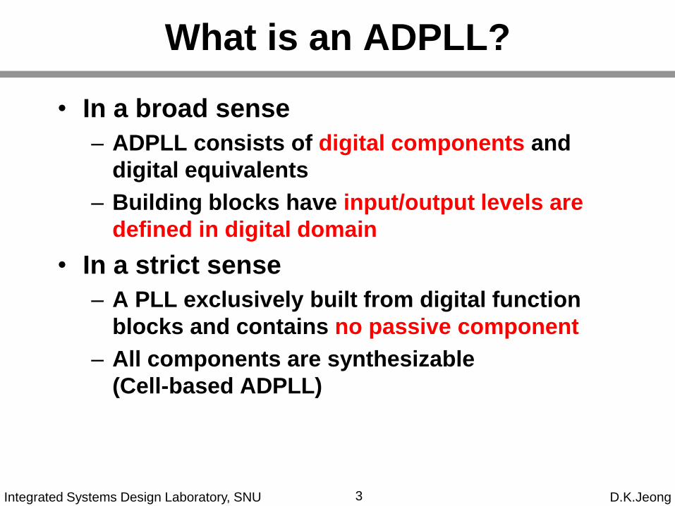
Analogy to Analog Filter (1)
• 1st order passive loop filter
R
C
Proportional term
Integral term
β
α
z-1
12

Integrated Systems Design Laboratory, SNU D.K.Jeong
• z-domain model
• 2nd order passive loop filter
21
21
1
21
,1
)1/(
1
)(
)1/()(
CRC
CC
RC
ssCC
ssH
pz
p
z
11 1
1
1)(
zzzH
1 1
1( )
1 1H z
z z
With gain normalization
Analogy to Analog Filter (2)
R
C1
C2
β
α
z-1
z-1
γ
Additional
low pass filter
13

Integrated Systems Design Laboratory, SNU D.K.Jeong
Adaptive Digital Loop Filter
• Lock-time control, frequency locking range
enhancement
• Find the optimum performance point
– Input noise filtering vs. lock-time
• Utilize software or hardware
– Gain estimation
– Noise cancellation
β
α
z-1
Adaptive
control
14

Integrated Systems Design Laboratory, SNU D.K.Jeong
TDC Classification
• Linear TDC
– Delay line based
– Fine resolution
– Consumes large hardware and power
– Process dependent and less reusable
• Bang-bang TDC
– Simple structure
– Highly nonlinear but can be controlled
– More reusable
15

Integrated Systems Design Laboratory, SNU D.K.Jeong
Linear TDC
• Converts time difference
to digital value
• Important design factors:
resolution, linearity,
power, area
• Conventional TDC
– Delay chain and samplers
– Minimum delay is
restricted by intrinsic gate
delay Vernier TDC,
interpolative TDC
– Large size, small dynamic
range
tf
QD
ts
QD
ts
QD QD
...
...
Decoder
Start
Stop
ts ts ts
tf tf tf tf
QD QD QD QD
...
...
Decoder
Start
Stop
...
[3] S. Henzler JSSC 2008
[2] P. Dudek JSSC 2000
16

Integrated Systems Design Laboratory, SNU D.K.Jeong
Linear TDC
• To increase dynamic
range
– Ring oscillator-based TDC
– Large power consumption
due to the free running
oscillator
• Stochastic TDC
– Exploits mismatch
between samplers and
random variation of the
offset voltage
– Very fine resolution
– Narrow range
...
Register
Start
Stop
Counters
Logic
Enable
QD QD QD QD
...
Encoder
Stop
...
Start
VOS1 VOS2 VOS3 VOSn
[4] J. Yu JSSC 2010
[5] V. Kratyuk TCASI 2009
17
Integrated Systems Design Laboratory, SNU D.K.Jeong
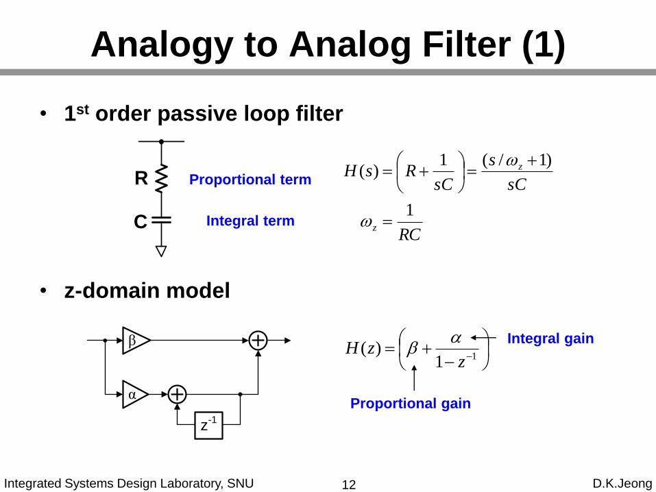
• Easily achievable and suitable for digital
implementation
– e.g. bang-bang PFD
Bang-Bang TDC
Conventional PFD Bang-bang PFD
DFF
DFF
reset
reset
Up
Down
Ref
Div
‘1’
‘1’
Conventional
PFD
Ref
Div
Up
Down
[6] T. Olsson JSSC 2004
18

Integrated Systems Design Laboratory, SNU D.K.Jeong
Digitally Controlled Oscillator
• Most Critical component
in ADPLL implementation
• Digital-to-frequency
conversion
– Underlying functionality is
analog
– Supports digital interface
– Analog nature doesn’t
propagate
• Implementation method
– Explicit DAC + VCO
– Embedded DAC (turning
on/off each unit cell)
DCO
DACVctrl
Digital
input
Clock
output
Explicit DAC + VCO
DCO
Oscillator
core
Digital
input
Clock
output
Embedded DAC
DecoderSwitch
Array
digital signals
...
...
...
......
...
...
...
en[0] en[1] en[2]
en[mn-1]
en[n-1]
en[(m-1)n]
e.g. ring DCO
19
Integrated Systems Design Laboratory, SNU D.K.Jeong
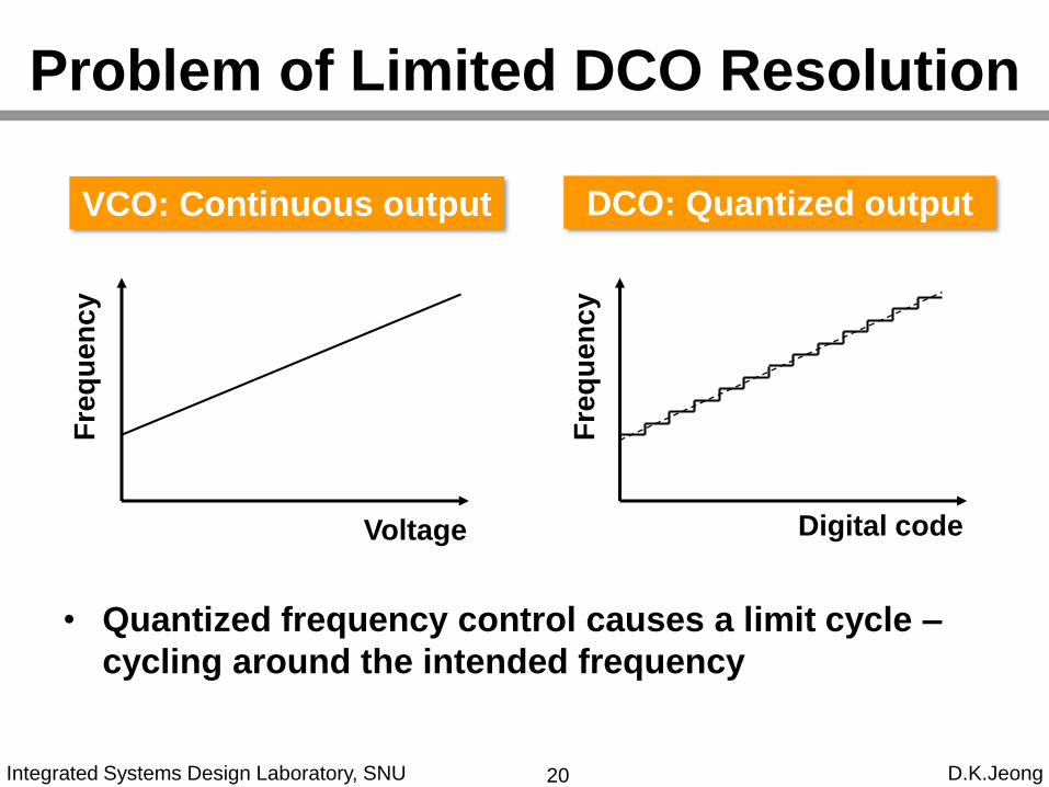
Problem of Limited DCO Resolution
• Quantized frequency control causes a limit cycle –
cycling around the intended frequency
Fre
qu
en
cy
Voltage
VCO: Continuous output
Digital code
Fre
qu
en
cy
DCO: Quantized output
20

Integrated Systems Design Laboratory, SNU D.K.Jeong
Typical Locked Behavior of ADPLL
• Periodic or pseudo-periodic (peak-to-peak jitter is
bounded)
• ΔΣ-modulator can be used to alleviate this problem
Ph
ase e
rro
r
Time
Phase error DCO control code
Time
Co
ntr
ol c
od
e
21

Integrated Systems Design Laboratory, SNU D.K.Jeong
TDC DLFError
cancellerΔΣ DCO
÷ M
÷ N/N+1
ΔΣ
• ΔΣ-modulator (ΔΣ) is used to increase the
effective resolution of the DCO
• Fractional spur can be reduced by using
cancellation techniques
ADPLL Architecture
[7] C.-M. Hsu JSSC 2008
[8] R. B. Staszewski JSSC 200522

Integrated Systems Design Laboratory, SNU D.K.Jeong
Low Jitter DCO Using ΔΣ-Modulator
• Effective frequency resolution is improved by high-
speed ΔΣ-dithering
• Higher update rate of DCO is important
– Phase error accumulates for dithering cycles
– Peak-to-peak jitter is inversely proportional to update
frequency
RefOut
fupdate = fRef
< Case 1 > < Case 2 >
TDC DLF DCO
÷ M
÷ N
fupdate = fOut/M fRef
TDC DLF ΔΣ DCOOut
÷ N
Ref
23

Integrated Systems Design Laboratory, SNU D.K.Jeong
Outline
• Introduction
• ADPLL Building Blocks
– Digital Loop Filter
– Digitally Controlled Oscillator
– Time-to-Digital Converter
• Modeling and Analysis
• Phase Noise
• Summary
24

Integrated Systems Design Laboratory, SNU D.K.Jeong
Analysis methods
• z-domain analysis
– Models discrete-time behavior
– Can exploit intuitive CPPLL analogy
– Quick and simple
• s-domain analysis
– z-to-s domain transformation
• Simple approximation (z -> 1+sT)
• Bilinear-z transformation (z -> (1+sT/2)/(1-sT/2))
– CPPLL analogy can be used
– Many s-domain analysis techniques reused
• Phase Margin
• Bandwidth
25

Integrated Systems Design Laboratory, SNU D.K.Jeong
TDC DCODLF
α
z-1
β z-D
z-1
γKTDC
Simple z-domain Model
• Stability check in z-domain
– Unit circle criterion: all poles should be inside the unit circle
– Jury’s stability criterion
TDCTDC
DDD
TDCTDC
D
TDCDCODLFTDC
KzKzzz
KzK
zL
zLzC
zz
z
αβKzHzHKzL
)(2
)(
)(1
)()(
11)()()(
11
11
26
𝑲𝑻𝑫𝑪 =𝑻
𝟐𝝅∆𝒕𝑻𝑫𝑪[LSB/rad]
= 𝟐𝝅∆𝒇𝑻[rad/LSB]

Integrated Systems Design Laboratory, SNU D.K.Jeong
• Step input:
• Error function:
• Using final value theorem:
Phase error is eventually eliminated
0)()1(
)1(
)1( lim
)()1( lim)(
21
31
1
1
TDCTDC
D
D
z
pz
p
KzKzz
zz
z
pz
zEze
1( ) ( ) ( )
1 ( 1)
p pzp t p u t P z
z z
TDCTDC
D
D
p
KzKzz
zz
z
pz
zL
zPzCzPzPzE
)()1(
)1(
)1(
)(1
)()()()()(
21
21
Steady-State Phase Error
27

Integrated Systems Design Laboratory, SNU D.K.Jeong
• Ramp input:
• Error function:
• Using final value theorem:
2)1()( )()(
z
wTzzFtuwttf
TDCTDC
D
D
f
KzKzz
zz
z
wTz
zL
zFzCzFzFzE
)()1(
)1(
)1(
)(1
)()()()()(
21
21
2
0)()1(
)1(
)1(lim
)()1( lim)(
21
31
21
1
TDCTDC
D
D
z
fz
f
KzKzz
zz
z
wTz
zEze
Steady-State Frequency Error
Frequency error is eventually eliminated
28

Integrated Systems Design Laboratory, SNU D.K.Jeong
Analysis Using CPPLL Analogy
• DLF coefficients selection
– Apply bilinear transform to s-domain filter
• Ts : sampling time of digital system
– Compare coefficients
1
1
1
12
z
z
Ts
s
1
1
1
22)(
z
zRC
TR
C
T
zH
ss
C
TR
C
T
s
s
2
sCRsH
1)(
1
1
1 11)(
z
z
zzH
[10] V. Kratyuk TCASII 2007
29

Integrated Systems Design Laboratory, SNU D.K.Jeong
Analysis Using CPPLL Analogy
• Use stability analysis method of CPPLL
– TS : Sampling period [s]
– TREF : Reference period (usually TREF = Ts)
– KDCO : DCO gain [Hz/LSB]
– ΔtTDC : Resolutions of TDC [s/LSB]
– PM : Phase Margin
– ωUGBW : Unit gain bandwidth [rad/s]
2
1tan(PM)
(PM)tan1 2
2
UGBWs
UGBW
DCO
TDC
REF
s
T
K
Nt
T
T
[10] V. Kratyuk TCASII 2007
30

Integrated Systems Design Laboratory, SNU D.K.Jeong
Analysis Using CPPLL Analogy
• Use stability analysis using simple approximation (z -> 1+sT)
31
21
( )
( ) 180
tan
TDC
Z
TDCUGBW
UGBW
TDC
αT s K β
sT sT
α
βT
K β
T
PM T j
K β
α
2 2 2
tan tan
UGBW UGBW TDC
TDC VCO
UGBW UGBW TDC
TDC VCO
T t
PM K PM K
T tβ
K β T K
UGBWZ
( )T j
2 2
1TDCK α
T s
1TDCK
T s
LSB / rad2
TDC
TDC
TK
t
2
2 rad/LSB
:[Hz/LSB]
DCO
DCO
DCO
f T
K T
K

Integrated Systems Design Laboratory, SNU D.K.Jeong
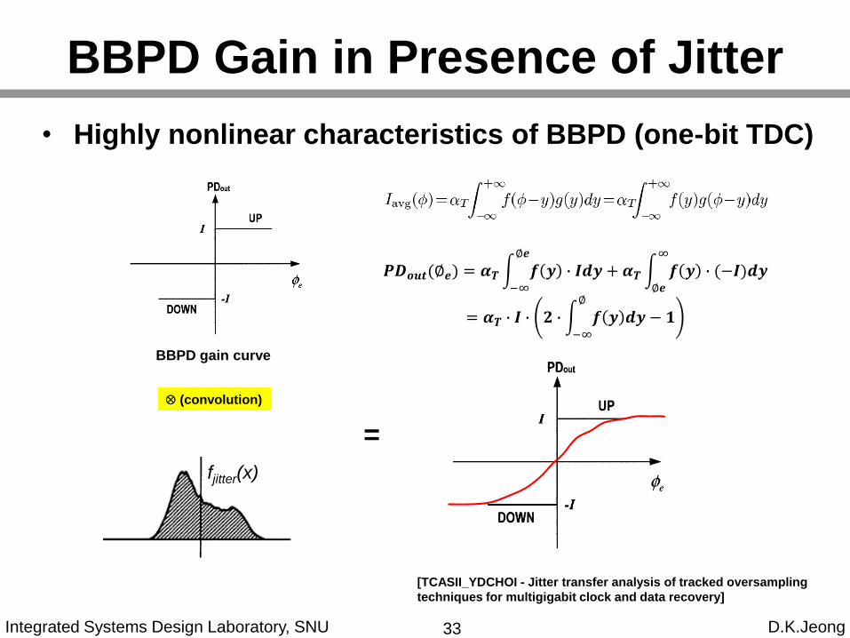
PD Gain in Presence of Jitter
• PD inputs contain jitter from input and VCO
32
[TCASII_YDCHOI - Jitter transfer analysis of tracked oversampling
techniques for multigigabit clock and data recovery]
Integrated Systems Design Laboratory, SNU D.K.Jeong
BBPD Gain in Presence of Jitter
• Highly nonlinear characteristics of BBPD (one-bit TDC)
33
[TCASII_YDCHOI - Jitter transfer analysis of tracked oversampling
techniques for multigigabit clock and data recovery]
BBPD gain curve
fjitter(x)
(convolution)
=
𝑷𝑫𝒐𝒖𝒕(∅𝒆) = 𝜶𝑻න−∞
∅𝒆
𝒇 𝒚 ∙ 𝑰𝒅𝒚 + 𝜶𝑻න∅𝒆
∞
𝒇 𝒚 ∙ (−𝑰)𝒅𝒚
= 𝜶𝑻 ∙ 𝑰 ∙ 𝟐 ∙ න−∞
∅
𝒇 𝒚 𝒅𝒚 − 𝟏
Integrated Systems Design Laboratory, SNU D.K.Jeong
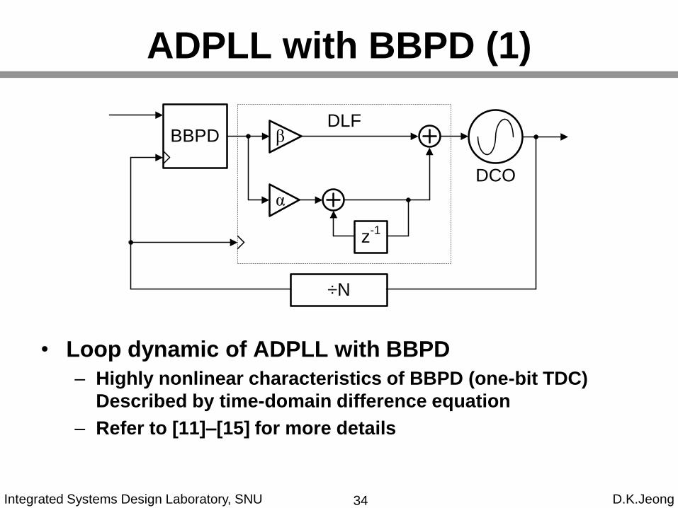
ADPLL with BBPD (1)
• Loop dynamic of ADPLL with BBPD
– Highly nonlinear characteristics of BBPD (one-bit TDC)
Described by time-domain difference equation
– Refer to [11]–[15] for more details
DLFBBPD β
α
z-1
DCO
÷N
34

Integrated Systems Design Laboratory, SNU D.K.Jeong
Nonlinear Loop Dynamics
• Nonlinear dynamics are illustrated by trajectories in
the phase space
• Behavior: equilibrium point or periodic orbit
State variable 1
Sta
te v
ari
ab
le 2
Unstable (diverge)
State variable 1
Sta
te v
ari
ab
le 2
Stable (converge)
35

Integrated Systems Design Laboratory, SNU D.K.Jeong
ADPLL with BBPD (2)
• Stability condition: Existence of limit-cycle
– Phase and frequency errors never converge to zero
concurrently
• Long pipeline stages increase loop latency
– Enlarge the size of orbit
– Degrade jitter performance
• Small loop latency is
important
Fre
qu
en
cy e
rro
r
Dynamics of ADPLL with BBPD
Phase error
36

Integrated Systems Design Laboratory, SNU D.K.Jeong
DNPDOUT
DCOin
Phase
DN
P0 P0+
DN
DN
DN
DNUP
UP
UP
UP
UP
P0 P0 P0 2
UP
UP
P0
DN
DN
P0 P0+
DN
Latency = 1, Jpp = 3
ADPLL with BBPD (3)
• 1st order BBPLL loop dynamics (initial error = 0)
– Peak-to-peak jitter is directly proportional to loop latency
Latency = D, JPP = (1 + 2D) [11] N. D. Dalt TCASI 2005
DNPDOUT
DCOin
Phase
UP
P0 P0
UP
DN
DN
UPDN
UP
DN
DN
P0 P0 P0
Latency = 0, Jpp =
37

Integrated Systems Design Laboratory, SNU D.K.Jeong
ADPLL with BBPD (4)
• 1st order BBPLL loop dynamics
– Initial error ≠ 0, JPP = 2(1+D)Δ
– For uniform distribution
• 2nd order BBPLL loop dynamics
– Size of orbit (stability) depends on D and R=α(int)/β(prop)
– For small R, JPP ≈ 2(1+D)Δ
– For uniform distribution and small orbit
22 2
2
(1 )
3
Jitter variance
Quantized Step of DCO
J
J
D
D Delay
22
2
3
)1(
DJ
)sgn(
)sgn(
11
1
kkk
DkDkkk R
[11] N. D. Dalt TCASI 2005
38

Integrated Systems Design Laboratory, SNU D.K.Jeong
Outline
• Introduction
• ADPLL Building Blocks
– Digital Loop Filter
– Digitally Controlled Oscillator
– Time-to-Digital Converter
• Modeling and Analysis
• Phase Noise
• Summary
39

Integrated Systems Design Laboratory, SNU D.K.Jeong
General Linearized s-domain Model
[16] M. H. Perrott JSSC 2002
TREF
2πHLF(z)
ΦREF
Φn,TDC
1
ΔtTDC
KDCO
jf
1
N
ΦOUT
Φn,DCOΦn,ΔΣ
T
DT-CT
TREF
1
TREF
CT-DT
)(1
)()(
1)(
1
2)(
fA
fAfG
Njf
KfH
t
TfA DCO
TDC
REF
Low bandwidth PLLf
S(f)Total noise
TDC noise
DCO noise
High bandwidth PLLf
S(f)Total noise
TDC noise
DCO noise
40
𝑫𝑪𝑶 𝒈𝒂𝒊𝒏 =
𝟏−𝒛−𝟏=
𝟐𝝅∆𝒇𝑻
𝒋𝟐𝝅𝒇𝑻=
𝑲𝑫𝑪𝑶
𝒋𝒇[rad/s/LSB]

Integrated Systems Design Laboratory, SNU D.K.Jeong
Spectral Density Conversion
H(f)x(t) y(t)
CT CT
H(ej2πfT)x[k] y[k]
DT DT
H(f)x[k] y(t)
DT CT
)()()(2
fSfHfS xy
)()()( 22
22 fTj
x
fTjfTj
y eSeHeS
)()(1
)( 22 fTj
xy eSfHT
fS
[16] M. H. Perrott JSSC 2002
41
Integrated Systems Design Laboratory, SNU D.K.Jeong
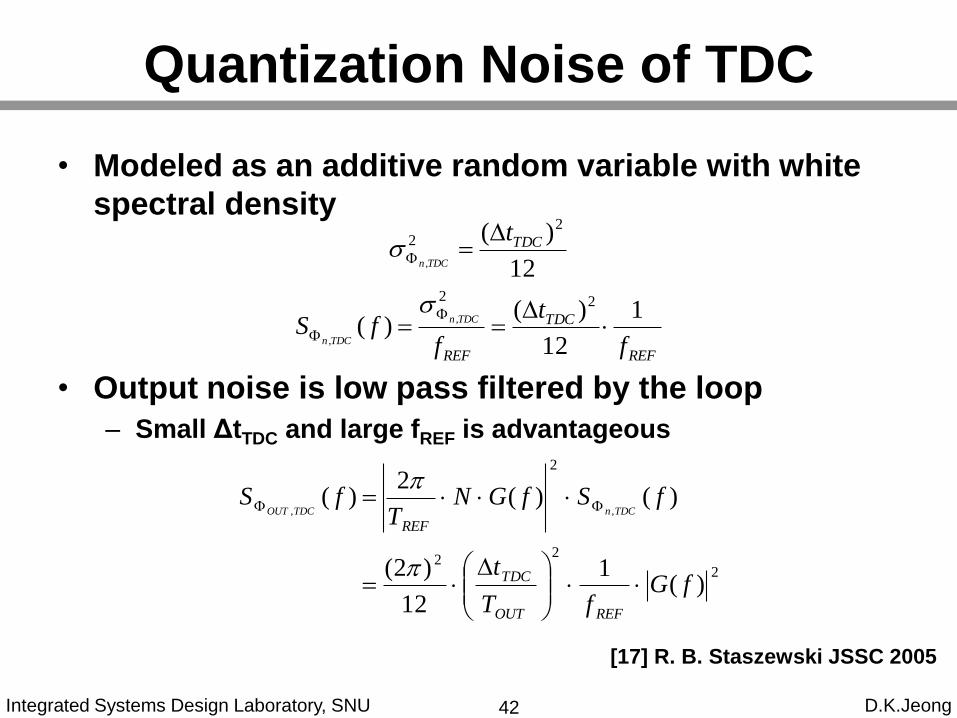
Quantization Noise of TDC
• Modeled as an additive random variable with white
spectral density
• Output noise is low pass filtered by the loop
– Small ΔtTDC and large fREF is advantageous
REF
TDC
REF
TDC
f
t
ffS
t
TDCn
TDCn
TDCn
1
12
)()(
12
)(
22
22
,
,
,
2
22
2
)(1
12
)2(
)()(2
)(,,
fGfT
t
fSfGNT
fS
REFOUT
TDC
REFTDCnTDCOUT
[17] R. B. Staszewski JSSC 2005
42

Integrated Systems Design Laboratory, SNU D.K.Jeong
Noises in Oscillator
• FM noise
– Up-converted flicker
noise (1/f3)
– Up-converted thermal
noise (1/f2)
• PM noise
– Thermal electronic
noise added from
outside of the oscillator
core (e.g. output buffer)
– High pass filtered by
the loop
PM noise: −170dBc/Hz
slope: −20dBc/Hz
FM noise: −153dBc/Hz
@ 20MHz
)()(1)(,,
2fSfGfS
DCOnDCOOUT
43
Integrated Systems Design Laboratory, SNU D.K.Jeong
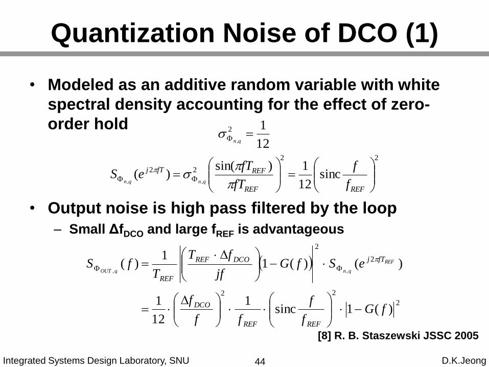
Quantization Noise of DCO (1)
• Modeled as an additive random variable with white
spectral density accounting for the effect of zero-
order hold
• Output noise is high pass filtered by the loop
– Small ΔfDCO and large fREF is advantageous
22
22
2
sinc12
1)sin()(
12
1
,,
,
REFREF
REFfTj
f
f
fT
fTeS
qnqn
qn
2
22
2
2
)(1sinc1
12
1
)()(11
)(,,
fGf
f
ff
f
eSfGjf
fT
TfS
REFREF
DCO
fTjDCOREF
REF
REF
qnqOUT
[8] R. B. Staszewski JSSC 2005
44

Integrated Systems Design Laboratory, SNU D.K.Jeong
DCO Dithering
• Discrete frequency level
– Frequency error always occurs
– DCO resolution is the limiting factor of the
phase noise performance
– Dithering by using ΔΣ modulation to enhance
resolution
– Dithering noise should be less than the natural
phase noise of the oscillator
– Caution: dithering increases high frequency
noise
45

Integrated Systems Design Laboratory, SNU D.K.Jeong
Quantization Noise of DCO (2)
• Power spectral density of quantization noise of nth
order ΔΣ dithering (fdth = M·fREF)
– High frequency noise increases
• Output noise is high pass filtered by the loop
n
REF
n
REFfTj
Mf
f
MM
fT
MeS
qn
n
222
2 sin212
1sin2)(
,
,
2
22
2
2
)(1sin21
12
1
)()(11
)(,,
fGf
f
ff
f
eSfGjf
fT
TfS
n
dthdth
DCO
fTjDCOREF
REF
REF
nOUT
[8] R. B. Staszewski JSSC 2005
46

Integrated Systems Design Laboratory, SNU D.K.Jeong
Quantization Noise of DCO (3)
• Noise shaping
– Performance bottleneck in some RF application
– Fine resolution is important even if dithering is used
• Peak value
• For 2nd order dithering
ΔfDCO = 554.4 kHz
ΔfDCO = 95.6 kHz
7.2for
195.0
)}(max{
2
,
dth
dth
DCO ff
ff
f
fSOUT
2nd order dithering,
f0 = 4GHz, fdth = 500 MHz
dth
n
dth
DCO
f
fr
r
rn
rn
rn
ff
f
fSOUT
and tan
for
1)(
)(41
12
1
)}(max{
2
22
,
47

Integrated Systems Design Laboratory, SNU D.K.Jeong
Time-Domain Noise (Jitter)
• Jitter
– Uncertainty or randomness in the timing of events
• Phase modulation jitter (PM jitter)
– Non-accumulative jitter
– Random fluctuation in the delay between input and output
event with zero mean and bounded variation
• Frequency modulation jitter (FM jitter)
– Accumulative jitter
– Uncertainty of when a transition occurs accumulates with
every transition
– Modeled as a random walk that is not bounded
[18] K. Kundert 2001
48
Integrated Systems Design Laboratory, SNU D.K.Jeong
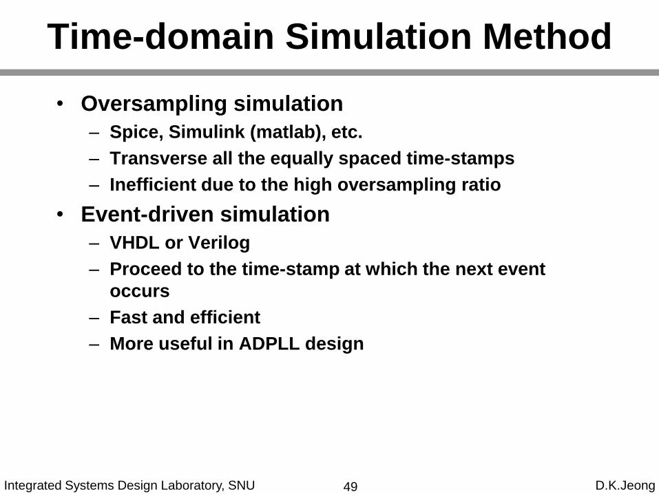
Time-domain Simulation Method
• Oversampling simulation
– Spice, Simulink (matlab), etc.
– Transverse all the equally spaced time-stamps
– Inefficient due to the high oversampling ratio
• Event-driven simulation
– VHDL or Verilog
– Proceed to the time-stamp at which the next event
occurs
– Fast and efficient
– More useful in ADPLL design
49

Integrated Systems Design Laboratory, SNU D.K.Jeong
Basic Time-Domain Equation
• For nominal frequency f0 and nominal period T0
• For small ΔT/T0
• Timing deviation (TDEV)
– The difference between actual and ideal timing
ΔTTff
0
0
1
2
0
2
0
0
0T
TTf
T
TfΔf
i
l
i
l f
lflTiTDEV
12
01
][][][
[19] R. B. Staszewski TCASI 2005
50

Integrated Systems Design Laboratory, SNU D.K.Jeong
Δt1 Δt2 Δt3 Δt4
T0 2T0 3T0 4T0
Actual time-stamps
Idea time-stamps
0
Oscillator PM Jitter
• Non accumulative addictive random error
• Timing errors do not influence one another
• Relation between time and frequency domains
][])[(][][ 000 itTiitTiTiitiTDEVPM
floor) noise :(2
00 LfL
Tt
[19] R. B. Staszewski TCASI 2005
51

Integrated Systems Design Laboratory, SNU D.K.Jeong
ΔT1 ΔT2 ΔT3 ΔT4
T0 2T0 3T0 4T0
Actual time-stamps
Idea time-stamps
T0T0
T0T0
0
Oscillator FM Jitter
• Accumulative jitter
• Each transition depends on all previous deviation
• Relation between time and frequency domains
i
l
i
l
FM lTTilTTiTiitiTDEV1
0
1
00 ][)][(][][
}{0
0
fLTf
fT
[19] R. B. Staszewski TCASI 2005
52

Integrated Systems Design Laboratory, SNU D.K.Jeong
Jitter and Phase Noise
• Convert phase noise specification into time-domain constraints
• FM jitter
– e.g. to meet −153 dBc/Hz @ 20 MHz for 1.9 GHz• 20 MHz/1.9 GHz x (0.53 ns x 10-15.3 /Hz)0.5 = 5.4 fsRMS
• PM jitter
– e.g. to meet −170 dBc/Hz for 1.9 GHz• 0.53 ns x (1.9 GHz x 10-17 /Hz)0.5 / 2π = 11.6 fsRMS
00
2fL
Tt
}{0
0
fLTf
fT
[22] http://www.jittertime.com/resources/pncalc.shtml
53

Integrated Systems Design Laboratory, SNU D.K.Jeong
Summary
• ADPLLs are similar to DSP systems
• ADPLL will be dominantly used in deep-
submicron technology
• DLF offers more flexibility in design
• TDC and DCO dominate overall performance
• Various techniques can be exploited to
analyze the ADPLL in both frequency and
time domain
54
Integrated Systems Design Laboratory, SNU D.K.Jeong
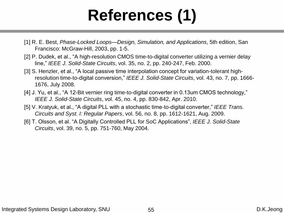
References (1)
[1] R. E. Best, Phase-Locked Loops—Design, Simulation, and Applications, 5th edition, San
Francisco: McGraw-Hill, 2003, pp. 1-5.
[2] P. Dudek, et al., “A high-resolution CMOS time-to-digital converter utilizing a vernier delay
line,” IEEE J. Solid-State Circuits, vol. 35, no. 2, pp. 240-247, Feb. 2000.
[3] S. Henzler, et al., “A local passive time interpolation concept for variation-tolerant high-
resolution time-to-digital conversion,” IEEE J. Solid-State Circuits, vol. 43, no. 7, pp. 1666-
1676, July 2008.
[4] J. Yu, et al., “A 12-Bit vernier ring time-to-digital converter in 0.13um CMOS technology,”
IEEE J. Solid-State Circuits, vol. 45, no. 4, pp. 830-842, Apr. 2010.
[5] V. Kratyuk, et al., “A digital PLL with a stochastic time-to-digital converter,” IEEE Trans.
Circuits and Syst. I: Regular Papers, vol. 56, no. 8, pp. 1612-1621, Aug. 2009.
[6] T. Olsson, et al. “A Digitally Controlled PLL for SoC Applications”, IEEE J. Solid-State
Circuits, vol. 39, no. 5, pp. 751-760, May 2004.
55

Integrated Systems Design Laboratory, SNU D.K.Jeong
References (2)
[7] C.-M. Hsu, et al., “A low-noise wide-BW 3.6-GHz digital ΔΣ fractional-N frequency
synthesizer with a noise-shaping time-to-digital converter and quantization noise
cancellation,” IEEE J. Solid-State Circuits, vol. 43, no. 12, pp. 2776-2786, Dec. 2008.
[8] R. B. Staszewski, et al., “A digitally controlled oscillator in a 90 nm digital CMOS process for
mobile phones,” IEEE J. Solid-State Circuits, vol. 40, no. 11, pp. 2203-2211, Nov. 2005.
[9] R. B. Staszewski, et al., “Phase-domain all-digital phase-locked loop,” IEEE Trans. Circuits
and Syst. II: Express Briefs, vol. 52. no 3, pp. 159-163, Mar. 2005.
[10] V. Kratyuk, et al., “A design procedure for all-digital phase-locked loops based on a charge-
pump phase-locked-loop analogy,” IEEE Trans. Circuits and Syst. II: Express Briefs, vol. 54,
no. 3, pp. 247-251, Mar. 2007.
[11] N. D. Dalt, “A design-oriented study of the nonlinear dynamics of digital bang-bang PLLs,”
IEEE Trans. Circuits and Syst. I: Regular Papers, vol. 52, no. 1, pp. 21-31, Jan. 2005.
56

Integrated Systems Design Laboratory, SNU D.K.Jeong
References (3)
[12] N. D. Dalt, “Markov chains-based derivation of the phase detector gain in bang-bang PLLs,”
IEEE Trans. Circuits Syst. II: Express Briefs, vol. 53, no. 11, pp. 1195-1199, Nov. 2006.
[13] N. D. Dalt, “ Linearized analysis of a digital bang-bang PLL and its validity limits applied to
jitter transfer and jitter generation,” IEEE Trans. Circuits and Syst. I: Regular Papers, vol. 55,
no. 11, pp. 3663-3675, Dec. 2008.
[14] B. Chun, el al., “Statistical properties of first-order bang-bang PLL with nonzero loop delay,”
IEEE Trans. Circuits and Syst. II: Express Briefs, vol. 55, no. 10, pp. 1016–1020, Oct. 2008.
[15] M. Zanuso, et al., “Noise analysis and minimization in bang-bang digital PLLs,” IEEE Trans.
Circuits and Syst. II: Express Briefs, vol. 56, no. 11, pp. 835–839, Nov. 2009.
[16] M. H. Perrott, et al., “A modeling approach for Σ-Δ fractional-N frequency synthesizers
allowing straightforward noise analysis,” IEEE J. Solid-State Circuits, vol. 37, no. 8, pp.
1028-1038, Aug. 2002.
57

Integrated Systems Design Laboratory, SNU D.K.Jeong
References (4)
[17] R. B. Staszewski, et al., “All-digital PLL and transmitter for mobile phones,” IEEE J. Solid-
State Circuits, vol. 40, no. 12, pp. 2469-2482, Dec. 2005.
[18] K. Kundert, Modeling and simulation of jitter in PLL frequency synthesizers, cadence white
paper, 2001.
[19] R. B. Staszewski, et al., “Event-driven simulation and modeling of phase noise of an RF
oscillator,” IEEE Trans. Circuits and Syst. I: Regular Papers, vol. 52. no 4, pp. 723-733, Apr.
2005.
[20] E. Temporiti, et al., “A 3 GHz fractional all-digital PLL with a 1.8 MHz bandwidth
implementing spur reduction techniques,” IEEE J. Solid-State Circuits, vol. 44, no. 3, pp.
824-834, Mar. 2009.
[21] M. Zanuso, et al., “A 3MHz-BW 3.6GHz digital fractional-N PLL with sub-gate-delay TDC,
phase-interpolation divider, and digital mismatch cancellation,” in IEEE ISSCC Dig. Tech.
Papers, 2010, pp. 476-477.
[22] http://www.jittertime.com/resources/pncalc.shtml
[23] YDCHOI - TCASII - Jitter transfer analysis of tracked oversampling techniques for
multigigabit clock and data recovery,” IEEE Trans. Circuits and Syst. II: Analog and Digital
Signal Processing, VOL 50, No 11, Nov 2003, pp. 775-783.
58

3.2. Digitally Controlled Oscillator
Deog-Kyoon Jeong
Integrated Systems Design Laboratory
Seoul National University

Integrated Systems Design Laboratory, SNU D.K.Jeong
• Basic Operation
• Requirements
• Classification
• Design Example
• Issues on DCO design
• Case Studies
2
Outline

Integrated Systems Design Laboratory, SNU D.K.Jeong
• A digital controlled oscillator (DCO) is the
digital counterpart of voltage controlled
oscillator (VCO) in an all digital phase locked
loop (ADPLL).
• Z-domain modeling
3
Basic Operation (1)
z-1
2pKDCOT

Integrated Systems Design Laboratory, SNU D.K.Jeong
• Input : N-bit digital code
• Output : periodic clock signal with frequency range (fmin ~ fmax)
• KDCO : Df (Hz/bit)
4
Basic Operation (2)
Control
code0 2N-1
Frequncy
fmin
fmax KDCO

Integrated Systems Design Laboratory, SNU D.K.Jeong
• Basic Operation
• Requirements
• Classification
• Design Example
• Issues on DCO design
• Case Studies
5
Outline

Integrated Systems Design Laboratory, SNU D.K.Jeong
• Fine frequency resolution (low KDCO)
• Wide range
– (Fine resolution + wide range) require larger N
• Linearity (constant Df/f)
• Low phase noise
• Low power consumption
• Small active area
6
DCO Requirements

Integrated Systems Design Laboratory, SNU D.K.Jeong
• Analog approach
– DAC + VCO
– DAC + ICO
– DAC + Varactor in LC tank
• Digital approach
– Control the number of inverter stages
– Control the number of drivers(variable inverter
strength)
– Control the C value in LC tank
– Control the divider with high freq. oscillator
7
DCO Classification (1)
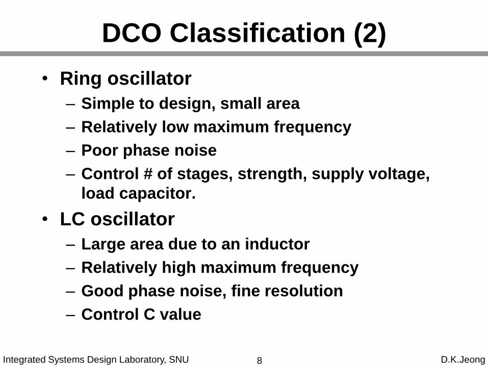
Integrated Systems Design Laboratory, SNU D.K.Jeong
• Ring oscillator
– Simple to design, small area
– Relatively low maximum frequency
– Poor phase noise
– Control # of stages, strength, supply voltage,
load capacitor.
• LC oscillator
– Large area due to an inductor
– Relatively high maximum frequency
– Good phase noise, fine resolution
– Control C value
8
DCO Classification (2)

Integrated Systems Design Laboratory, SNU D.K.Jeong
• Basic Operation
• Requirements
• Classification
• Design Example
• Issues on DCO design
• Case Studies
9
Outline

Integrated Systems Design Laboratory, SNU D.K.Jeong
• IDAC + analog VCO
– Control the R value
10
Analog approach (1)
[1] V. Kratyuk, SOVC, 2006
load swing
d eq load
C VT R C
I
IDAC inp inm
outm outp
Analog
voltage

Integrated Systems Design Laboratory, SNU D.K.Jeong
• IDAC + analog VCO
– Control the current
11
Analog approach (2)
load swing
d eq load
C VT R C
I
IDAC
Analog
current

Integrated Systems Design Laboratory, SNU D.K.Jeong
• DAC + analog VCO
– Control the voltage
12
Analog approach (3)
load swing
d eq load
C VT R C
I
d1 d2 d3 d4 d5
DAC
Supply
voltage
[2] D.Oh, ISSCC, 2007

Integrated Systems Design Laboratory, SNU D.K.Jeong
MUX
Coarse control :
stage selection Output
In
EN[1]
EN[n]
Out
EN[0]
Fine control :
Strength selection
Fine control
Fine control :
Combination delay path
• Stage selection + strength control
– All components are cell-based
13
Digital approach (1)
[3] T.-Y.Hsu, TCAS II, 2001
[4] Ching-Che Chung, JSSC, 2003

Integrated Systems Design Laboratory, SNU D.K.Jeong
• Strength control
14
Digital approach (2)
[5] T. Olsson, JSSC, 2004
RUNEN[0]
EN[6]
EN[12]
EN[120]
EN[7]
EN[13]
EN[121]
EN[1]
EN[11]
EN[17]
EN[127]
EN[5]

Integrated Systems Design Laboratory, SNU D.K.Jeong
• 2-phase selection + phase interpolating
– Control logic includes a FSM
15
Digital approach (3)
[6] S. Sidiropoulos, JSSC, 1997
N:2 MUX
Coarse control OutputPI
Fine control

Integrated Systems Design Laboratory, SNU D.K.Jeong
• High freq. oscillator + integer freq. divider
– Low resolution
– Used for wide-range applications
16
Digital approach (4)
/N divider
N control code
Fixed high freq.
oscillator
Clock output

Integrated Systems Design Laboratory, SNU D.K.Jeong
LC DCOs (1)
• Frequency tuning scheme
– Capacitance tuning
• MOS capacitance tuning
• For coarse/fine control
– Inductance tuning
• Self/mutual inductance tuning
• For band selection or coarse
control
• Suitable for dual mode
operation
Capacitor bank
Ctrl
Ctrl
Ctrl
17
LC
10
Integrated Systems Design Laboratory, SNU D.K.Jeong
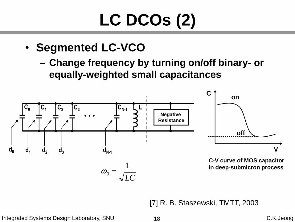
• Segmented LC-VCO
– Change frequency by turning on/off binary- or
equally-weighted small capacitances
18
LC DCOs (2)
[7] R. B. Staszewski, TMTT, 2003
CN-1
Negative
Resistance
C0 C1 C2 C3
d0 d1 d2 d3 dN-1
L
on
off
V
C
C-V curve of MOS capacitor
in deep-submicron process
LC
10

Integrated Systems Design Laboratory, SNU D.K.Jeong
• Basic Operation
• Requirements
• Classification
• Design Example
• Issues on DCO design
• Case Studies
19
Outline

Integrated Systems Design Laboratory, SNU D.K.Jeong
• Capacitive tuning:
– To enhance frequency resolution
• Increase capacitance
• Low LC-tank Q due to the parasitic capacitance
• Phase noise performance degradation
• Increased power consumption due to large load
capacitance
– Trade-off between frequency resolution, output
frequency, tuning range, and power
consumption
20
Trade-offs in LCDCOs
C
C
f
f D
D
2
1
0

Integrated Systems Design Laboratory, SNU D.K.Jeong
• Reducing switching noise
– Minimizing on/off switching
– Only one column bit state changes
21
Design Issues (1)
[2] D. Oh, ISSCC, 2007
Column Decoder
Ro
w D
ec
od
er
Control
code
Next row
row
col
rowcol
SW
Next row
row
colb
rowcolb
SW
Even row cell Odd row cell

Integrated Systems Design Laboratory, SNU D.K.Jeong
Design Issues (2)
• Frequency resolution
– Quantization noise due to uniform dithering
– Quantization noise due to ΣΔ modulation
– Directly affect phase noise performance
– Performance bottleneck in some application
22
[9] R. B. Staszewski, JSSC, 2005
22
sinc1
12
1)(
D
dthdth
res
f
f
ff
ffS
n
dthdth
res
f
f
ff
ffS
22
sin21
12
1)(
D
D
p

Integrated Systems Design Laboratory, SNU D.K.Jeong
• Choice for negative gm device
– NMOS
• Smallest parasitic capacitance for same gm
• Output swing exceeds the supply voltage
– PMOS
• Lower 1/f noise in most process(not always)
– CMOS
• Large parasitic capacitance
• Low signal distortion
• Min. & Max. output voltage is fixed
23
Design Issues (3)

Integrated Systems Design Laboratory, SNU D.K.Jeong
• Noise on current source
– The drain node of the current source has a
ripple of 2x output frequency
– Additional LC for high Z to the current source
24
Design Issues (4)
[9] R. B. Staszewski, JSSC, 2005Bias
L2 C2 High Z
L1
C1
L1
C111
0
1
CL
22
0
12
CL

Integrated Systems Design Laboratory, SNU D.K.Jeong
• Current source sizing
– According to the operating frequency, the
optimum size changes
– Digital code controls the current source
25
Design Issues (5)
[8] R. B. Staszewski, JSSC, 2005
Bias
L1
C1
L1
C1
Integrated Systems Design Laboratory, SNU D.K.Jeong
• Basic Operation
• Requirements
• Classification
• Design Example
• Issues on DCO design
• Case Studies
26
Outline

Integrated Systems Design Laboratory, SNU D.K.Jeong27
Monotonic DCO (1)
• Core oscillator : inverter-based 4-stage delay element
– Integral word control supply of the core oscillator
– PD outputs altering load capacitor
integral word<10:0>
Vvdddco
DCR
CBYPASS
Level
ConverterLevel
Converter
Level
Converter
Level
Converter
up
dnb
proportional
gain<3:0>
4-phase clock ( mclk<3:0> )
[16] H. Song, JSSC

Integrated Systems Design Laboratory, SNU D.K.Jeong
Monotonic DCO (2)
• Digitally controlled
resistor (DCR)
– Stacked row cells of PMOS
array
– monotonic characteristics
• Linear characteristics by
non-uniformly sizing of
wP1, wP2, … , wP31
on<0> on<1> on<31>
WS
onl<32> on<33> on<63>
on<992> on<993> on<1023>
WP0 WP1 WP31
fine<0>
28
[16] H. Song, JSSC

Integrated Systems Design Laboratory, SNU D.K.Jeong29
Monotonic DCO (3)
• Simulation results of the DCR with non-uniformly
sized parallel PMOSs
– Resistance range : 330 Ω ~ 3.3 kΩ
same width: RS0=RS, RP0=RP1= ··· =RP31
Non-uniform sizing: RS0>RS, RP0>RP1> ··· >RP31
0 100 200 300 400 500 600 700 800 900 1000
-2.5
-2
-1.5
-1
-0.5
0x 10
-3
code
no
rma
lize
d d
iffe
rentia
l re
sis
tance
same width
nonlinear sizing
same width
non-uniform sizing
RS0
RTOP=RS0
(31-N)×RS
(31-N)
RS
RS
RS
RS
N
RVARI=RP0//RP1// ••• // RPM
RF
RP0 RP1 RP30 RP31
RP0 RP1 RP30 RP31
RP0 RP1 RPM
REQUIV=RTOP // RVARI+(31-N)*RS+RFVvdddco
REQUIV=RTOP // RVARI+(31-N)*RS
integral word=25*N+M (N,M=0~31)
[16] H. Song, JSSC

Integrated Systems Design Laboratory, SNU D.K.Jeong
• Implementation of the DCR
30
Monotonic DCO (4)
Column decoder
Ro
w d
ec
od
er
MP0 MP1 MP31
MP0 MP1 MP31
MP0 MP1 MP31
MS0
MS
MS
col<0> col<30>
row<0>
row<1>
integral word<10:6>
integral word<6:1>
row<2>
MP0 MP1 MP31
MP0 MP1 MP31
MS
MS
row<29>
row<30>
Vvdddco
integral word<0>
MSE MF
[16] H. Song, JSSC

Integrated Systems Design Laboratory, SNU D.K.Jeong
• Supply-compensated delay cell
– Coarse : stage selector
– Fine : phase interpolator
31
V-Tolerant DCO (1)
[14] B. M. Moon, TCAS II, 2008

Integrated Systems Design Laboratory, SNU D.K.Jeong
• Supply-compensated delay cell
– The strength of the latch is controlled by Vth
(PMOS) and VDD – Vth (NMOS).
32
V-Tolerant DCO (2)
[14] B. M. Moon, TCAS II, 2008

Integrated Systems Design Laboratory, SNU D.K.Jeong
• Supply-compensated delay cell
– Delay time is insensitive to the supply voltage.
33
V-Tolerant DCO (3)
[14] B. M. Moon, TCAS II, 2008

Integrated Systems Design Laboratory, SNU D.K.Jeong
• DCO code prediction for fast locking
– Using reference clock, PVT sensor detects
current condition.
– DCO code prediction makes a fast locking
34
Fast locking ADPLL (1)
[15] H. S. Jeon, ISCAS, 2008
(a) DCO
(b) PVT sensor

Integrated Systems Design Laboratory, SNU D.K.Jeong
• DCO code prediction for fast locking
– By normalizing, PVT variation can be cancelled
35
Fast locking ADPLL (2)
[15] H. S. Jeon, ISCAS, 2008
(a) DCO period (b) DCO normalized period
Predicted codeword for 6ns period
Integrated Systems Design Laboratory, SNU D.K.Jeong
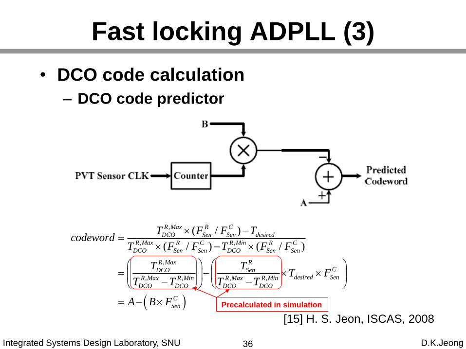
• DCO code calculation
– DCO code predictor
36
Fast locking ADPLL (3)
[15] H. S. Jeon, ISCAS, 2008
,
, ,
,
, , , ,
( / )
( / ) ( / )
R Max R C
DCO Sen Sen desired
R Max R C R Min R C
DCO Sen Sen DCO Sen Sen
R Max RCDCO Sen
desired SenR Max R Min R Max R Min
DCO DCO DCO DCO
C
Sen
T F F Tcodeword
T F F T F F
T TT F
T T T T
A B F
Precalculated in simulation

Integrated Systems Design Laboratory, SNU D.K.Jeong
• Hysteresis delay cell
– Coarse stage : selecting delay path
– Fine stage : hysteresis delay cell
37
Fine-Resolution DCO (1)
[13] D. Sheng, TCAS II, 2007
MUX
Coarse control :
stage selection
Fine delay
pathOut
F1ON[1] F1ON[2]
HDC

Integrated Systems Design Laboratory, SNU D.K.Jeong
• Hysteresis delay cell
38
Fine-Resolution DCO (2)
[13] D. Sheng, TCAS II, 2007
F1ON
I1 I3
I 2
F1ON
F1ON
Cload
I 1 I3
N1N1
I 2
High for a
while

Integrated Systems Design Laboratory, SNU D.K.Jeong
• Phase noise of LC DCO is affected by the
frequency resolution
• Δf is linearly proportional to ΔC
• Output frequency: ~ GHz
– Required Δf: ~ kHz
– Required minimum ΔC: ~ aF
– Minimum ΔC depends on the minimum feature
size of the process
– Various studies focus on ΔC minimization
39
Frequency Resolution

Integrated Systems Design Laboratory, SNU D.K.Jeong
• Capacitors in series
• Capacitive divider network
• Vulnerable to process variation, parasitic,
and mismatch
40
Capacitance Minimization Techniques
Out+ Out-
Control
2C2
2C1 2C1
2C2
R/2 R/2
Out+ Out-
CCCC
CCeq D
D
2
210
2
[18] Y. Chen, A-SSCC, 2007
[17] X. Dai, ISIC, 2009

Integrated Systems Design Laboratory, SNU D.K.Jeong
• NMOS-PMOS varactor bank
41
Fine-Resolution LC-DCO (1)
[11] J. H. Han, EL, 2008

Integrated Systems Design Laboratory, SNU D.K.Jeong
• NMOS-PMOS varactor bank
– Capacitance of MOSFET in various process
42
Fine-Resolution LC-DCO (2)
[11] J. H. Han, EL, 2008
ProcessNMOS PMOS NMOS-PMOS
Con Coff ΔC Con Coff ΔC Con Coff ΔC
65nm 200a 104a 96a 183a 94a 89a 294a 287a 7a
90nm 253a 143a 110a 266a 159a 107a 413a 409a 4a
130nm 3.7f 2.0f 1.7f 3.4f 1.6f 1.8f 5.2f 5.4f -0.2f
180nm 4.2f 2.2f 2.0f 4.6f 2.5f 2.1f 6.7f 6.8f -0.1f

Integrated Systems Design Laboratory, SNU D.K.Jeong
• NMOS-PMOS varactor bank
– Quality factors of the varactors
43
Fine-Resolution LC-DCO (3)
[11] J. H. Han, EL, 2008
PMOS
NMOS
N-PMOS
Integrated Systems Design Laboratory, SNU D.K.Jeong
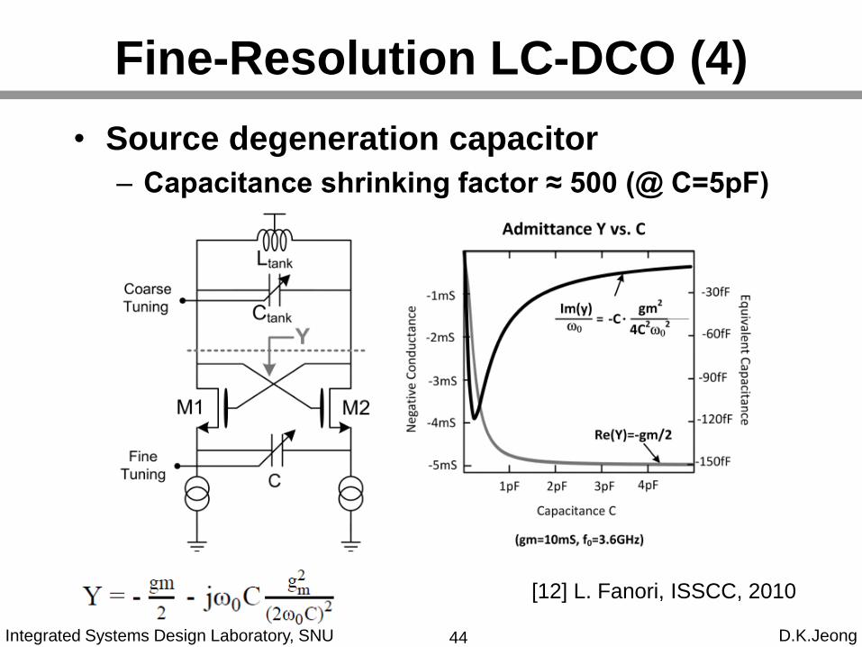
• Source degeneration capacitor
– Capacitance shrinking factor ≈ 500 (@ C=5pF)
44
Fine-Resolution LC-DCO (4)
[12] L. Fanori, ISSCC, 2010

Integrated Systems Design Laboratory, SNU D.K.Jeong
• Source degeneration capacitor
45
Fine-Resolution LC-DCO (5)
[12] L. Fanori, ISSCC, 2010

Integrated Systems Design Laboratory, SNU D.K.Jeong
• Source degeneration capacitor
– Adding 4-bit DAC for higher resolution
46
Fine-Resolution LC-DCO (6)
[12] L. Fanori, ISSCC, 2010
@ 3.3GHz with shrinking factor of 150
300f HzD

Integrated Systems Design Laboratory, SNU D.K.Jeong
• Dual-LC tank DCO
– Only one -gm cell is intended to be enabled
47
Dual-LC Tank DCO (1)
[19] A. Goel, SOVC, 2010L1=2.05nH, L2=1.28nH, k12=0.3

Integrated Systems Design Laboratory, SNU D.K.Jeong
• Coupled inductors
– Behavior of active tank is influenced by the inactive tank
– Adjusting the resonance frequency of inactive tank
results in three modes
48
Dual-LC Tank DCO (2)
[19] A. Goel, SOVC, 2010

Integrated Systems Design Laboratory, SNU D.K.Jeong
• Performance summary
49
Dual-LC Tank DCO (3)
Integrated Systems Design Laboratory, SNU D.K.Jeong50
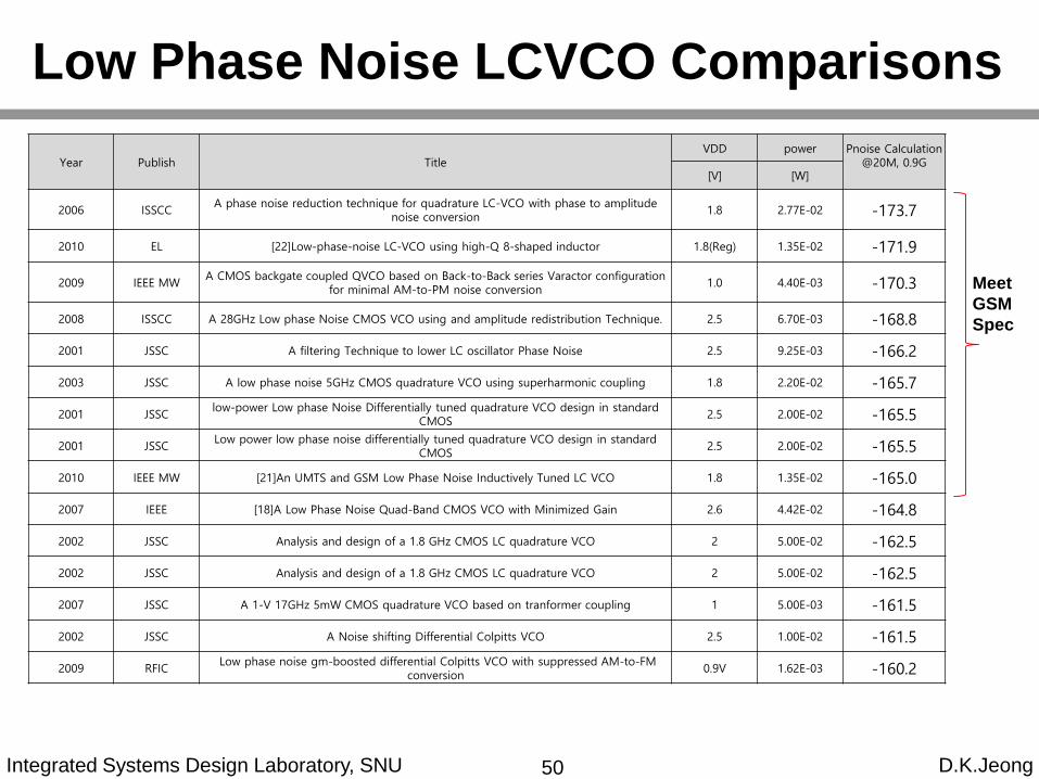
Low Phase Noise LCVCO Comparisons
Year Publish TitleVDD power Pnoise Calculation
@20M, 0.9G[V] [W]
2006 ISSCCA phase noise reduction technique for quadrature LC-VCO with phase to amplitude
noise conversion1.8 2.77E-02 -173.7
2010 EL [22]Low-phase-noise LC-VCO using high-Q 8-shaped inductor 1.8(Reg) 1.35E-02 -171.9
2009 IEEE MWA CMOS backgate coupled QVCO based on Back-to-Back series Varactor configuration
for minimal AM-to-PM noise conversion1.0 4.40E-03 -170.3
2008 ISSCC A 28GHz Low phase Noise CMOS VCO using and amplitude redistribution Technique. 2.5 6.70E-03 -168.8
2001 JSSC A filtering Technique to lower LC oscillator Phase Noise 2.5 9.25E-03 -166.2
2003 JSSC A low phase noise 5GHz CMOS quadrature VCO using superharmonic coupling 1.8 2.20E-02 -165.7
2001 JSSClow-power Low phase Noise Differentially tuned quadrature VCO design in standard
CMOS2.5 2.00E-02 -165.5
2001 JSSCLow power low phase noise differentially tuned quadrature VCO design in standard
CMOS2.5 2.00E-02 -165.5
2010 IEEE MW [21]An UMTS and GSM Low Phase Noise Inductively Tuned LC VCO 1.8 1.35E-02 -165.0
2007 IEEE [18]A Low Phase Noise Quad-Band CMOS VCO with Minimized Gain 2.6 4.42E-02 -164.8
2002 JSSC Analysis and design of a 1.8 GHz CMOS LC quadrature VCO 2 5.00E-02 -162.5
2002 JSSC Analysis and design of a 1.8 GHz CMOS LC quadrature VCO 2 5.00E-02 -162.5
2007 JSSC A 1-V 17GHz 5mW CMOS quadrature VCO based on tranformer coupling 1 5.00E-03 -161.5
2002 JSSC A Noise shifting Differential Colpitts VCO 2.5 1.00E-02 -161.5
2009 RFICLow phase noise gm-boosted differential Colpitts VCO with suppressed AM-to-FM
conversion0.9V 1.62E-03 -160.2
Meet
GSM
Spec

Integrated Systems Design Laboratory, SNU D.K.Jeong51
Wide Tuning Ranges LCVCO Comparisons
Year Publish TitleInductor
Tuning method
Truning range
Freq [Hz]
Process
VDD power Pnoise Calculation@20M,0.9Gmax/min
x100min center max [V] W
2006 MTTSwitched resonator and Their Application in a dual band
monolithic CMOS LC-Tuned VCOSelf
7,9n/3.2n 110.6 1.64E+09 1.73E+09 1.81E+09 0.18u 3.3~3.6 1.6E-02 -159.5
2008 JSSCDesign of wide Tuning-Range CMOS VCOs using switched
coupled-inductorsMutual 160.1 7.34E+09 9.55E+09 1.18E+10 90n 1.2 7.7E-03 -154.3
2009 JSSCLC PLL with 1.2-Octave Locking Range based on mutual-
inductance switching in 45nm SOI CMOS
Mutualk=0.48
0.1n/0.2n239.7 7.30E+09 1.24E+10 1.75E+10 45n 1 1.4E-02 -141.7
2005 RFITMulti-mode wide-band 130 nm CMOS WLAN and GSM-
UMTSMutual 334.8 3.42E+09 7.44E+09 1.15E+10 0.13u 1.5 3.0E-03 -163.9
2007 MTTNew Frequency Plan and Reconfigurable 6.6- 7.128 GHz CMOS Quadrature VCO for MB OFDM UWB Application
Self 108.0 6.60E+09 6.86E+09 7.13E+09 0.18u 2 2.0E-02 -159.3
2000 CICCA new approach to fully integrated CMOS LC-oscillators
with a very large tuning rangeSelf 159.7 1.34E+09 1.74E+09 2.14E+09 0.35u 3 - -132.5
2007 ELWide tuning range LC-oscillator in 65nm SOI CMOS,
based on switchable secondary inductorMutual
0.6n/0.3n 176.6 6.40E+09 8.85E+09 1.13E+10 65n 1 4.5E-03 -143.8
2007 JSSC A Magnetically Tuned Quadrature OscillatorMutual + K
control 228.1 3.20E+09 5.25E+09 7.30E+09 65n 1.2 2.4E-02 -150.1
2009 RFIC1.1 to 1.9GHz CMOS VCO for Tuner Application with
Resistively Tuned Variable InductorMutual + R 177.4 1.06E+09 1.47E+09 1.88E+09 0.25u 3 2.0E-02 -148.4
2005 ASSCCA 1V Dual-Band VCO Using an Integrated Variable
InductorMutual + C 513.6 2.20E+09 6.75E+09 1.13E+10 0.18u 1 5.0E-03 -154.5
2009 CICCA CMOS 3.3-8.4 GHz wide tuning range, low phase noise
LC VCOSelf 254.5 3.30E+09 5.85E+09 8.40E+09 0.13u 1.6 1.5E-02 -162.4
2002 ESSCIRCESSCIRC A CMOS fully integrated 1 GHz and 2 GHz dual
band VCO with a voltage controlled inductorSelf 200.0 1.00E+09 1.50E+09 2.00E+09 0.25u 1.5 1.4E-02 -155.4
2007 RFITA Dual Band CMOS Quadrature VCO for Low Power and
Low Phase Noise ApplicationSelf 272.2 1.80E+09 3.35E+09 4.90E+09 0.18u 1.7 6.8E-03 -155.0
None can meet GSM spec.(-165dBc/Hz @ 900MHz freq, 20MHz offset).
There is trade-off between tuning range and phase noise.

Integrated Systems Design Laboratory, SNU D.K.Jeong
[1] V. Kratyuk, et al. “A digital PLL with a stochastic time-to-digital
converter” IEEE SOVC, Dig. Tech. Paper, June. 2006.
[2] D. Oh, et al., “A 2.8Gbs All-Digital CDR with a 10b Monotonic DCO,”
IEEE ISSCC Dig. Tech. Papers, 2007.
[3] T.-Y. Hsu, et al. “Design and analysis of a portable high-speed clock
generator,” IEEE Trans. on Circuits and Systems. II, Apr. 2001.
[4] C.-C. Chung, et al. “An all-digital phase-locked loop for high speed
clock generation,” IEEE J. Solid-State Circuits, Feb. 2003.
[5] T. Olsson, et al. “A Digitally Controlled PLL for SoC Applications,” IEEE
J. Solid-State Circuits, Vol. 39, No. 5, May 2004, pp 751-760, Feb.
2003.
[6] S. Sidiropoulos, et al., “A semidigital dual delay-locked loop,” IEEE J.
Solid-State Circuits, Nov. 1997.
[7] R. B. Staszewski, et al. “A first multigigahertz digitally controlled
oscillator for wireless applications,” IEEE Trans. on Microwave Theory
and Techniques, Vol. 51. No. 11, Nov. 2003.
52
Reference(1)

Integrated Systems Design Laboratory, SNU D.K.Jeong
[8] R. B. Staszewski, et al. “All-Digital PLL and Transmitter for Mobile
Phones,” IEEE J. Solid-State Circuits, vol. 40, no. 12, pp. 2469-2482,
Dec. 2005.
[9] R. B. Staszewski, et al. “A digitally controlled oscillator in a 90nm digital
CMOS process for mobile phones,” IEEE J. Solid-State Circuits, vol. 40,
no. 11, pp. 2203-2211, Nov. 2005.
[10] H. Shi, et al., “Variable Negative Gm Technique for RF LC VCO with
Very Large Tuning Range,” in Electron Devices and Solid-State Circuits,
2005 IEEE Conference on, pp. 145-148, 2005.
[11] J. H. Han, et al., “Digitally controlled oscillator with high frequency
resolution using novel varactor bank,” IEEE Electronics Letters, vol. 44,
no. 25, pp. 830-842, Dec. 2008.
[12] L. Fanori, et al., “3.3GHz DCO with a Frequency Resolution of 150Hz
for All-Digital PLL,” IEEE ISSCC Dig. Tech. Papers, pp. 48-49, 2010.
[13] D. Sheng, et al., “An Ultra-Low-Power and Portable Digitally
Controlled Oscillator for SoC Applications,” IEEE Trans. on Circuits and
systems - II, Vol 54. No. 11, Mar. 2007.
53
Reference(2)

Integrated Systems Design Laboratory, SNU D.K.Jeong
[14] B. M. Moon, et al., “Monotonic Wide-Range Digitally Controlled
Oscillator Compensated for Supply Voltage Variation,” IEEE Trans. on
Circuits and Systems II, Vol 55. No. 10, Oct. 2008.
[15] H. S. Jeon, et al., “Fast Frequency Acquisition All-Digital PLL Using
PVT Calibration,” IEEE International Symposium on Circuits and
Systems, 2008.
[16] H. Song, et al., “A 1.0–4.0-Gb/s All-Digital CDR With 1.0-ps Period
Resolution DCO and Adaptive Proportional Gain Control,” IEEE J.
Solid-State Circuits, to be published.
[17] X. Dai, et al., “Frequency resolution enhancement for digitally
controlled oscillators using series switched varactor,” ISIC, 2009, pp.
397-400.
[18] Y. Chen, et al., “9 GHz dual-mode digitally controlled oscillator for
GSM/UMTS transceivers in 65 nm CMOS,” IEEE A-SSCC, 2007, pp.
432-435.
[19] A. Goel, et al., “A compact 6 GHz to 12 GHz digital PLL with coupled
dual-LC tank DCO,” IEEE SOVC, Dig. Tech. Paper, 2010, pp. 141-142.
54
Reference(3)
3.3. Time-to-DigitalConverter
Deog-Kyoon Jeong
Integrated Systems Design Laboratory
Seoul National University

Integrated Systems Design Laboratory, SNU D.K.Jeong
• Introduction
• Basic Operation
• TDC Requirements
• TDC Classification
– Short time interval generation
– Time stretching
– Etc
2
Outline
Integrated Systems Design Laboratory, SNU D.K.Jeong
• Time-to-digital converter(TDC) is a device for converting a time difference between two events into a digital representation of their time indices.– Time-of-fight(TOF) measurement in high energy
particle physics, laser range finding and positive electron tomography(PET) medical imaging technology
– On-chip timing and jitter measurements
– Phase difference measurement in All-digital PLL and All-digital DLL
3
Introduction

Integrated Systems Design Laboratory, SNU D.K.Jeong4
Basic Operation(1)
Integrated Systems Design Laboratory, SNU D.K.Jeong
• TDC transfer curve
5
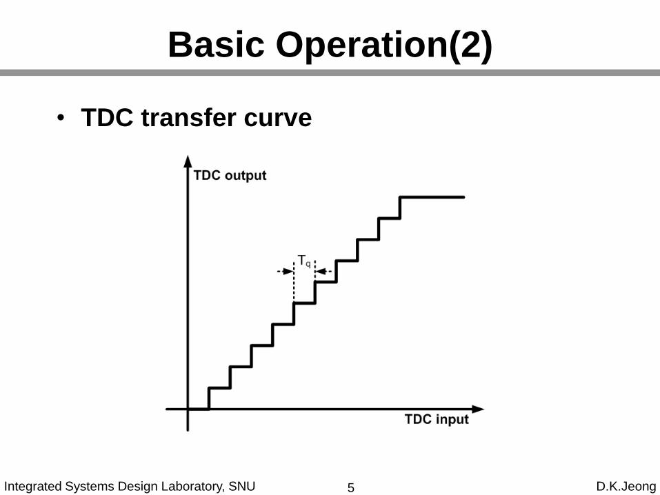
Basic Operation(2)

Integrated Systems Design Laboratory, SNU D.K.Jeong
• High resolution
• Wide range
• Linearity(INL, DNL)
• Low power
• Small area
6
TDC Requirements

Integrated Systems Design Laboratory, SNU D.K.Jeong
• Introduction
• Basic Operation
• TDC Requirements
• TDC Classification
– Short time interval generation
– Time stretching
– Etc
7
Outline

Integrated Systems Design Laboratory, SNU D.K.Jeong
• Short time interval generation
• Time Stretching
• Etc
– Gated ring oscillator TDC
– Pulse shrinking TDC
– Stochastic TDC
– Utilizing ADC
8
TDC Classification
Integrated Systems Design Laboratory, SNU D.K.Jeong
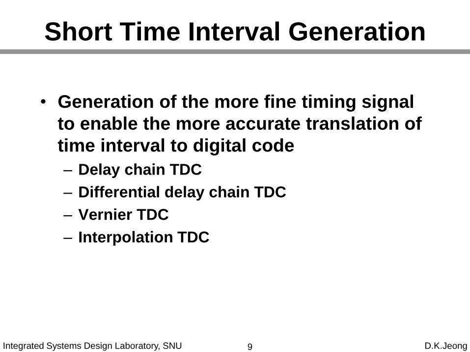
• Generation of the more fine timing signal
to enable the more accurate translation of
time interval to digital code
– Delay chain TDC
– Differential delay chain TDC
– Vernier TDC
– Interpolation TDC
9
Short Time Interval Generation

Integrated Systems Design Laboratory, SNU D.K.Jeong
• Two-inverter delay resolution
10
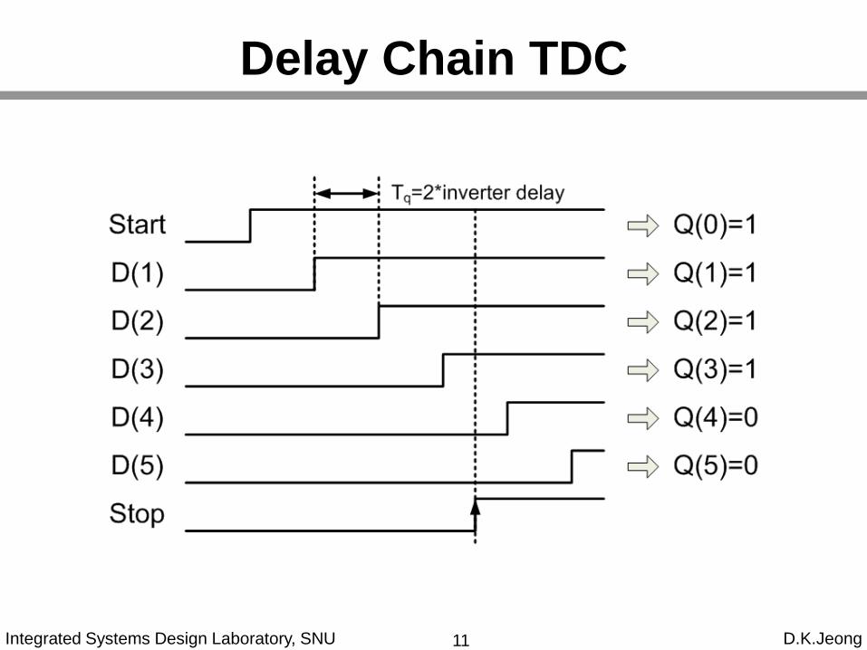
Delay Chain TDC
[1] Rahkonen,Ciruit and Systems,1989
Integrated Systems Design Laboratory, SNU D.K.Jeong11
Delay Chain TDC

Integrated Systems Design Laboratory, SNU D.K.Jeong
• One-inverter delay resolution
• Different setup time for data ‘1’ and ‘0’
12
Differential Delay Chain TDC

Integrated Systems Design Laboratory, SNU D.K.Jeong
• One-inverter delay resolution
• Using symmetric DFF
13
Differential Delay Chain TDC
[2]Staszewski,TSCASII,2006

Integrated Systems Design Laboratory, SNU D.K.Jeong
• Symmetric DFF
– Same setup time for data ‘1’ and ‘0’
14
Differential Delay Chain TDC
[3]Nikolic,JSSC,2000

Integrated Systems Design Laboratory, SNU D.K.Jeong
• Sub-gate-delay resolution
• TDC resolution = ts – tf , (ts ≠ tf )
15
Vernier TDC
[4]Dudek,JSSC,2000

Integrated Systems Design Laboratory, SNU D.K.Jeong16
Vernier TDC
Integrated Systems Design Laboratory, SNU D.K.Jeong
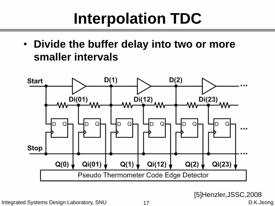
• Divide the buffer delay into two or more
smaller intervals
17
Interpolation TDC
[5]Henzler,JSSC,2008

Integrated Systems Design Laboratory, SNU D.K.Jeong18
Interpolation TDC
Integrated Systems Design Laboratory, SNU D.K.Jeong
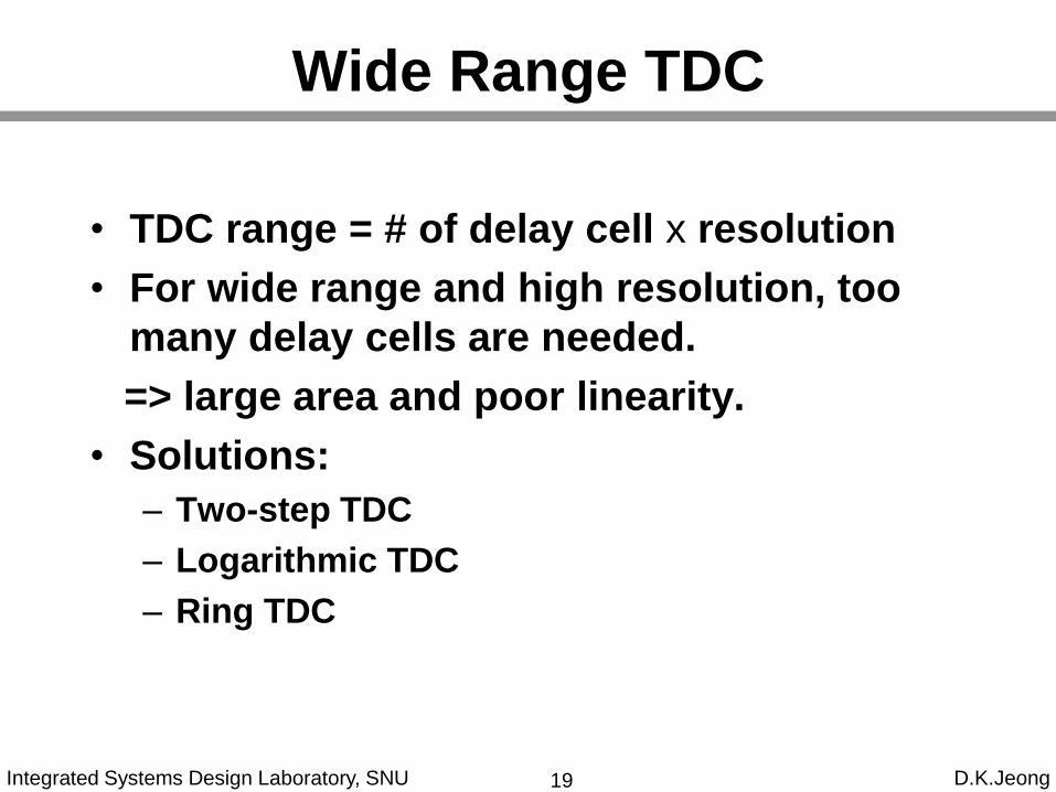
• TDC range = # of delay cell x resolution
• For wide range and high resolution, too
many delay cells are needed.
=> large area and poor linearity.
• Solutions:
– Two-step TDC
– Logarithmic TDC
– Ring TDC
19
Wide Range TDC

Integrated Systems Design Laboratory, SNU D.K.Jeong
• Incorporates both the delay chain TDC and
Vernier TDC
20
Two-Step TDC
[6]Ramakrishnan,VLSI Design,2006

Integrated Systems Design Laboratory, SNU D.K.Jeong
• Incorporates both the delay chain TDC and
Vernier TDC
21
Two-Step TDC (1)
[7]Tokairin,ISSCC,2010

Integrated Systems Design Laboratory, SNU D.K.Jeong22
Two-Step TDC (2)
[7]Tokairin,ISSCC,2010

Integrated Systems Design Laboratory, SNU D.K.Jeong
• SEL=high => measures td1 for normalization
• SEL=low => measures residue from delay chain
TDC
23
Two-Step TDC (3)
[7]Tokairin,ISSCC,2010

Integrated Systems Design Laboratory, SNU D.K.Jeong
• Wide range is achieved through logarithmic
inverter delay
• Additional logic is required for linearization
24
Logarithmic TDC
[8]Lin,ISSCC,2004

Integrated Systems Design Laboratory, SNU D.K.Jeong25
Logarithmic TDC

Integrated Systems Design Laboratory, SNU D.K.Jeong
• Reuses the delay elements and increases the
detection range
• Better linearity than delay chain TDC
26
Cyclic TDC
[9]Chang,ISSCC,2008
Inconsistency may occur
during transition

Integrated Systems Design Laboratory, SNU D.K.Jeong27
Vernier Ring TDC
[10]Yu,JSSC,2010

Integrated Systems Design Laboratory, SNU D.K.Jeong28
Vernier Ring TDC

Integrated Systems Design Laboratory, SNU D.K.Jeong
• Opposite approach to get high resolution
is time stretching
• Amplifies input time difference and uses
simple delay chain TDC
• Amplification greatly relaxes the
requirement on device matching in delay
line
– Time amplifying TDC
– Sub-exponent TDC
29
Time Stretching TDC

Integrated Systems Design Laboratory, SNU D.K.Jeong
• Time residue is amplified by TA(Time Amplifier)
and resolved by fine TDC
30
Time Amplifying TDC (1)
[13]Lee, JSSC 2008

Integrated Systems Design Laboratory, SNU D.K.Jeong31
Time Amplifying TDC (2)
[13]Lee, JSSC 2008

Integrated Systems Design Laboratory, SNU D.K.Jeong
• In SR latch followed by an XOR, the propagation delay
varies as an even-symmetric logarithmic function versus
input time difference.
32
Time Amplifying TDC (3)
[13]Lee, JSSC 2008

Integrated Systems Design Laboratory, SNU D.K.Jeong33
Time Amplifying TDC (4)
[13]Lee, JSSC 2008

Integrated Systems Design Laboratory, SNU D.K.Jeong34
Sub-Exponent TDC (1)
[14]Lee, JSSC 2010
• Scaling of resolution according to input time difference

Integrated Systems Design Laboratory, SNU D.K.Jeong35
Sub-Exponent TDC (1)
[14]Lee, JSSC 2010
td=
Output is 1 when time
difference is > td

Integrated Systems Design Laboratory, SNU D.K.Jeong
• First discharging is performed by two identical path
• Second discharging is perform by only one path
=> The gain of TA roughly is twice of the small signal input gain.
36
Sub-Exponent TDC (2)
[14]Lee, JSSC 2010

Integrated Systems Design Laboratory, SNU D.K.Jeong
• With large input time diff, output saturated. To get accurate
2x time amplification, TA calibration is necessary
37
Sub-Exponent TDC (3)
[14]Lee, JSSC 2010
PMOS diodes:
Slow discharge
on C & D
M1 and M3 not
completely
turned off
Integrated Systems Design Laboratory, SNU D.K.Jeong
• Etc
– Gated ring oscillator TDC
– Pulse shrinking TDC
– Stochastic TDC
– Time-to-Voltage followed by ADC
38
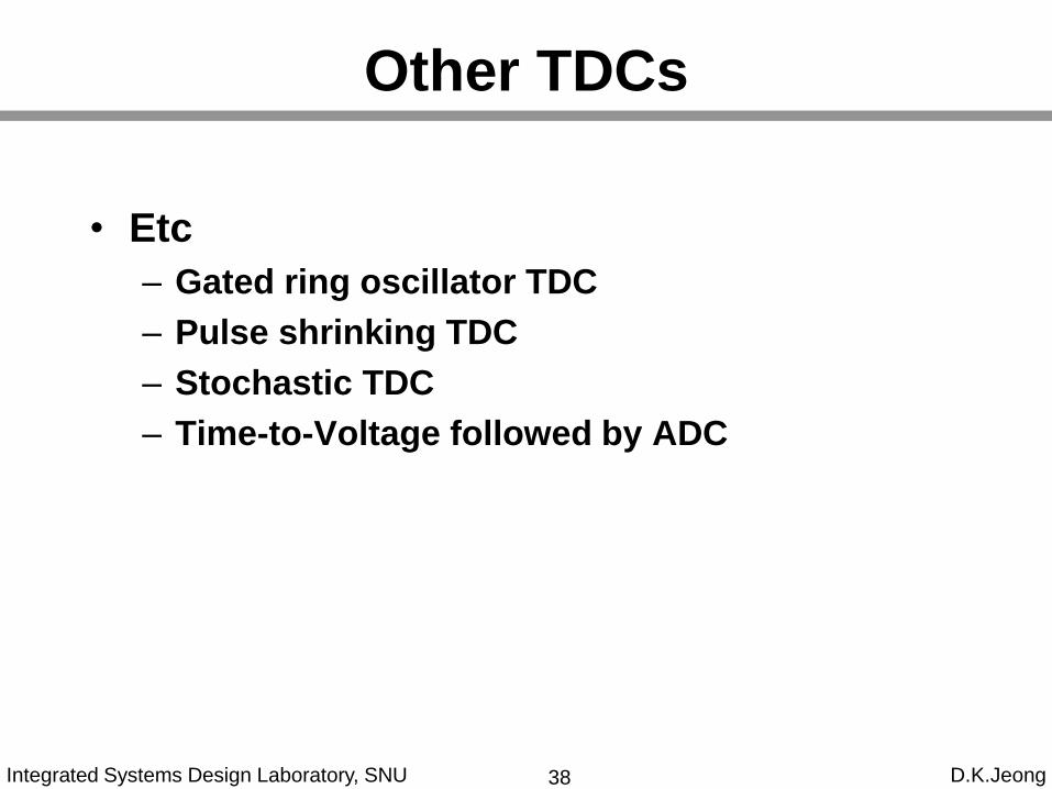
Other TDCs

Integrated Systems Design Laboratory, SNU D.K.Jeong
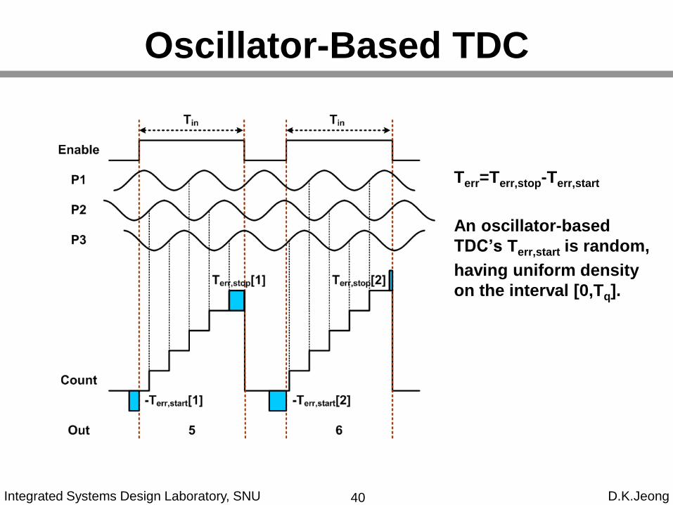
• Counters operate when enable signal is high
• Oscillator runs freely regardless of input
=> Large power consumption
39
Oscillator-Based TDC
[15]Nissinen,ESSCIRC,2003
Integrated Systems Design Laboratory, SNU D.K.Jeong
Terr=Terr,stop-Terr,start
An oscillator-based
TDC’s Terr,start is random,
having uniform density
on the interval [0,Tq].
40
Oscillator-Based TDC
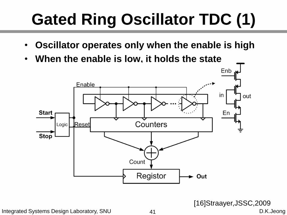
Integrated Systems Design Laboratory, SNU D.K.Jeong
• Oscillator operates only when the enable is high
• When the enable is low, it holds the state
41
Gated Ring Oscillator TDC (1)
[16]Straayer,JSSC,2009

Integrated Systems Design Laboratory, SNU D.K.Jeong
• When the enable is low, the time residue is stored
in VOi node
42
Gated Ring Oscillator TDC (2)
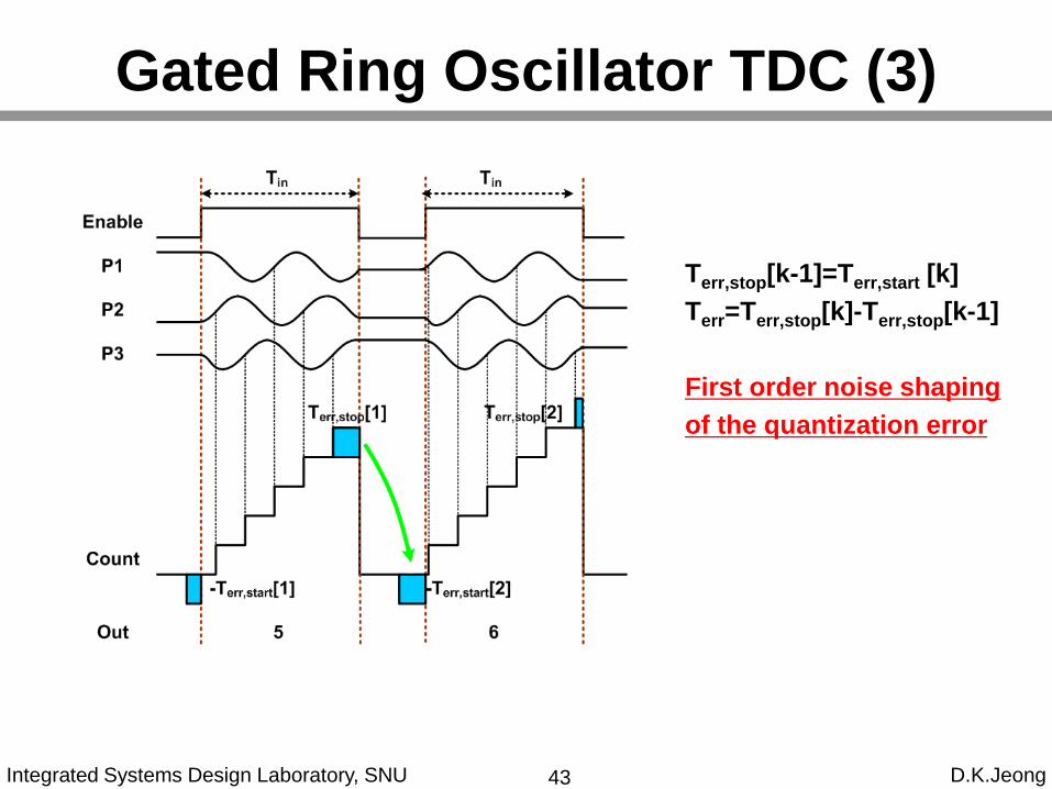
Integrated Systems Design Laboratory, SNU D.K.Jeong
Terr,stop[k-1]=Terr,start [k]
Terr=Terr,stop[k]-Terr,stop[k-1]
First order noise shaping
of the quantization error
43
Gated Ring Oscillator TDC (3)

Integrated Systems Design Laboratory, SNU D.K.Jeong
• Width of the input pulse shrinks in each element
by a fixed amount, until the pulse entirely
disappears.
44
Pulse Shrinking TDC (1)
[17] Karadamoglou,JSSC,2004

Integrated Systems Design Laboratory, SNU D.K.Jeong
• The propagation of the rising edge of the input
pulse is slowed down by the current starving
transistor.
45
Pulse Shrinking TDC (2)

Integrated Systems Design Laboratory, SNU D.K.Jeong
• Using random sampling offset mismatch
46
Stochastic TDC
[18]Kratyuk,TCASI,2009
Integrated Systems Design Laboratory, SNU D.K.Jeong
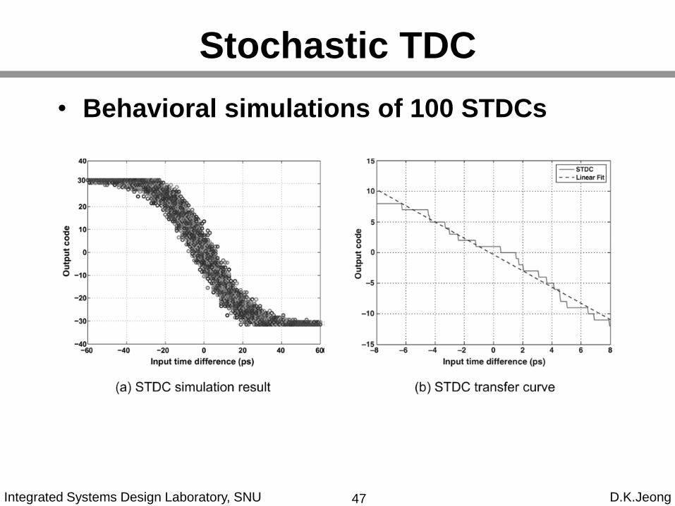
• Behavioral simulations of 100 STDCs
47
Stochastic TDC

Integrated Systems Design Laboratory, SNU D.K.Jeong
• The time interval is first converted into a voltage
and then the voltage is converted into a digital
value by ADC
48
Time-to-Voltage followed by ADC
[19] Maatta, Instrum.&Meas,1998

Integrated Systems Design Laboratory, SNU D.K.Jeong
[1] T. Rahkonen, et al., "Time interval measurements using integrated
tapped CMOS delay lines," in Circuits and Systems, vol.1, pp. 201-205,
Aug. 1989.
[2] R. B. Staszewski, et al., “1.3 V 20 ps time-to-digital converter for
frequency synthesis in 90 nm CMOS,” IEEE Trans. Circuits Syst. II,
Exp. Briefs, vol. 53, no. 3, pp. 220–224, Mar. 2006.
[3] B. N. Nikolic, et al., “Improved sense-amplifier-based flip-flop: design
and measurements,” IEEE J. Solid-State Circuits, vol. 35, no. 6, pp.
876–884, Jun. 2000.
[4] P. Dudek, et al., "A high-resolution CMOS time-to-digital converter
utilizing a vernier delay line," IEEE J. Solid-State Circuits, vol. 35, no. 2,
pp. 240-247, Feb. 2000.
[5] S. Henzler, et al., "A local passive time interpolation concept for
variation-tolerant high-resolution time-to-digital conversion," IEEE J.
Solid-State Circuits, vol. 43, no. 7, pp. 1666-1676, July 2008.
[6] V. Ramakrishnan, et al., “A wide-range, high-resolution, compact,
CMOS time to digital converter,” Proc. VLSI Design (VLSID’06), pp.
197-202, Jan. 2006.
49
Reference(1)

Integrated Systems Design Laboratory, SNU D.K.Jeong
[7] T. Tokairin, et al., "A 2.1-to-2.8GHz all-digital frequency synthesizer
with a time-windowed TDC," in IEEE ISSCC Dig. Tech. Papers, 2010,
pp. 470-471.
[8] J. Lin, B., et al., "A PVT tolerant 0.18MHz to 600MHz self-calibrated
digital PLL in 90nm CMOS process," in IEEE ISSCC Dig. Tech. Papers,
2004, pp. 488-541.
[9] C. Hsiang-Hui, et al., "A fractional spur-free ADPLL with loop-gain
calibration and phase-noise cancellation for GSM/GPRS/EDGE," in
IEEE ISSCC Dig. Tech. Papers, 2008, pp. 200-201.
[10]Jianjun Yu, et al., "A 12-Bit vernier ring time-to-digital converter in
0.13um CMOS technology," IEEE J. Solid-State Circuits, vol. 45, no. 4,
pp. 830-842, Apr. 2010.
[11] H. Chorng-Sii, et al., "A high-precision time-to-digital converter using a
two-level conversion scheme," IEEE Trans. Nucl. Sci., vol. 51, no. 4, pp.
1349-1352, Aug. 2004.
50
Reference(2)

Integrated Systems Design Laboratory, SNU D.K.Jeong
[12] C. Poki, et al., "A PVT insensitive vernier-based time-to-digital
converter with extended input range and high accuracy," IEEE Trans.
Nucl. Sci., vol. 54, no. 2, pp. 294-302, Apr. 2007.
[13] L. Minjae and A. A. Abidi, "A 9 b, 1.25 ps resolution coarse-fine time-
to-digital converter in 90 nm CMOS that amplifies a time residue," IEEE
J. Solid-State Circuits, vol. 43, no. 4, pp. 769-777, Apr. 2008.
[14] L. Seon-Kyoo, et al., "A 1GHz ADPLL with a 1.25ps minimum-
resolution sub-exponent TDC in 0.18um CMOS," in IEEE ISSCC Dig.
Tech. Papers, 2010, pp. 482-483.
[15] I. Nissinen, et al., "A CMOS time-to-digital converter based on a ring
oscillator for a laser radar," in Proc. IEEE ESSCIRC, 2003, pp. 469-472.
[16] M. Z. Straayer and M. H. Perrott, "A multi-path gated ring oscillator
TDC with first-order noise shaping,” IEEE J. Solid-State Circuits, vol. 44,
no. 4, pp. 1089-1098, Apr. 2009.
51
Reference(3)

Integrated Systems Design Laboratory, SNU D.K.Jeong
[17] K. Karadamoglou, et al., "An 11-bit high-resolution and adjustable-
range CMOS time-to-digital converter for space science instruments,"
IEEE J. Solid-State Circuits, vol. 39, no. 1, pp. 214-222, Jan. 2004.
[18] V. Kratyuk, et al., "A digital PLL with a stochastic time-to-digital
converter," IEEE Trans. Circuits and Syst. I, Reg. Papers, vol. 56, no. 8,
pp. 1612-1621, Aug. 2009.
[19] K. Maatta and J. Kostamovaara, “A high-precision time-to-digital
converter for pulsed time-of-flight laser radar applications,” IEEE Trans.
Instrum. Meas., vol. 47, no. 2, pp. 521–536, Apr. 1998.
[20] M. Straayer, “Noise shaping techniques for analog and time to digital
converters using voltage controlled oscillators,” Ph.D. dissertation, MIT,
Cambridge, MA, 2008.
[21] J. Kalisz, “Review of methods for time interval measurements with
picosecond resolution,” Metrologia, vol. 41, no. 1, pp. 17–32, Feb. 2004.
52
Reference(4)

3.4. All-Digital Frequency Synthesizer
Deog-Kyoon Jeong
Integrated Systems Design Laboratory
Seoul National University

Integrated Systems Design Laboratory, SNU D.K.Jeong
• Introduction
• Recently Published Frequency Synthesizers
Outline
2
Integrated Systems Design Laboratory, SNU D.K.Jeong
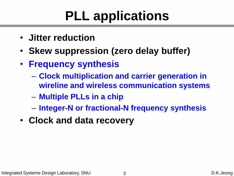
• Jitter reduction
• Skew suppression (zero delay buffer)
• Frequency synthesis
– Clock multiplication and carrier generation in
wireline and wireless communication systems
– Multiple PLLs in a chip
– Integer-N or fractional-N frequency synthesis
• Clock and data recovery
PLL applications
3

Integrated Systems Design Laboratory, SNU D.K.Jeong
TDC DLFError
cancellerΔΣ DCO
÷ M
÷ N/N+1
ΔΣ
• ΔΣ-modulator (ΔΣ) is used to increase the
effective resolution of the DCO
• Fractional spur can be reduced by using
cancellation techniques
ADPLL Fractional-N FS Architecture
[1] C.-M. Hsu JSSC 2008
[2] R. B. Staszewski JSSC 2005
4

Integrated Systems Design Laboratory, SNU D.K.Jeong
DCO Resolution Enhancement Using ΔΣ-Modulator
• We can’t reduce DCO resolution which is determined by
physical characteristics.
• However we can improve effective resolution of DCO by
averaging a modulated signals.
• ΔΣ-dithering means to change frequency with high modulation
frequency.
• Dithering prevents a jitter being accumulated. There only
short-term jitter. (In other word, high frequency noise
component)
Ideal
No dithering
With dithering
5

Integrated Systems Design Laboratory, SNU D.K.Jeong
High Resolution DCO Using ΔΣ-Modulator
• Effective frequency resolution is improved by high-
speed ΔΣ-dithering
• Higher update rate of DCO is important
– Phase error accumulates for dithering cycles
– Peak-to-peak jitter is inversely proportional to update
frequency
RefOut
fupdate = fRef
< Case 1 > < Case 2 >
TDC DLF DCO
÷ M
÷ N
fupdate = fOut/M fRef
TDC DLF ΔΣ DCOOut
÷ N
Ref
6

Integrated Systems Design Laboratory, SNU D.K.Jeong
• Peak-to-peak jitter reduction
Low Jitter DCO Using ΔΣ-Modulator
Lock point
Δte,pp ≈ N x KD
Tdiv,m Tdiv,m+1
Td,k Td,k+1
Tref Tref
Ref
Div
Out
Δte,m
Lock point
Δte,pp ≈ M x KD
Td,k = KD x DCOin,k
KD : DCO resolution
< Case 1 > < Case 2 >
Td,k+N-1
M = fOut/fΔΣ
RefOut
fupdate = fRef
< Case 1 >
TDC DLF DCO
÷ N
< Case 2 >
÷ M
fupdate = fOut/M fRef
TDC DLF ΔΣ DCOOut
÷ N
Ref
7

Integrated Systems Design Laboratory, SNU D.K.Jeong
• Design issue
– Synchronization between lower and higher frequency
clock domain
– Fast ΔΣ-dithering speed for low jitter generation
– Noise shaping due to ΔΣ
• High frequency noise increases
• Performance bottleneck in some RF applications
Low Jitter DCO Using ΔΣ-Modulator
High frequency regionLow frequency region
÷ M
TDC DLF ΔΣ DCO
÷ N
Synchronization
OutRef
8

Integrated Systems Design Laboratory, SNU D.K.Jeong
Frequency Multiplication
• General fractional-N operation
– Divider dithering using ΔΣ
• Phase-domain operation
– Accumulate frequency
control word (FCW)
RefOut
TDC DLF DCO
÷ N/N+1
ΔΣ
ΣN.F
Ref Σ
DLF DCOOut
1
+
−
9

Integrated Systems Design Laboratory, SNU D.K.Jeong
• Phase-domain operation
– Long term average: fRef × N = fOut × 1
– Reference and output clock domains are not
synchronous
– Spurious tones occur
Integer Frequency Multiplication
ΣN
LF DCO
1Σ
+Out
Ref
+
−
[3] R. B. Staszewski TCASII 2005
10
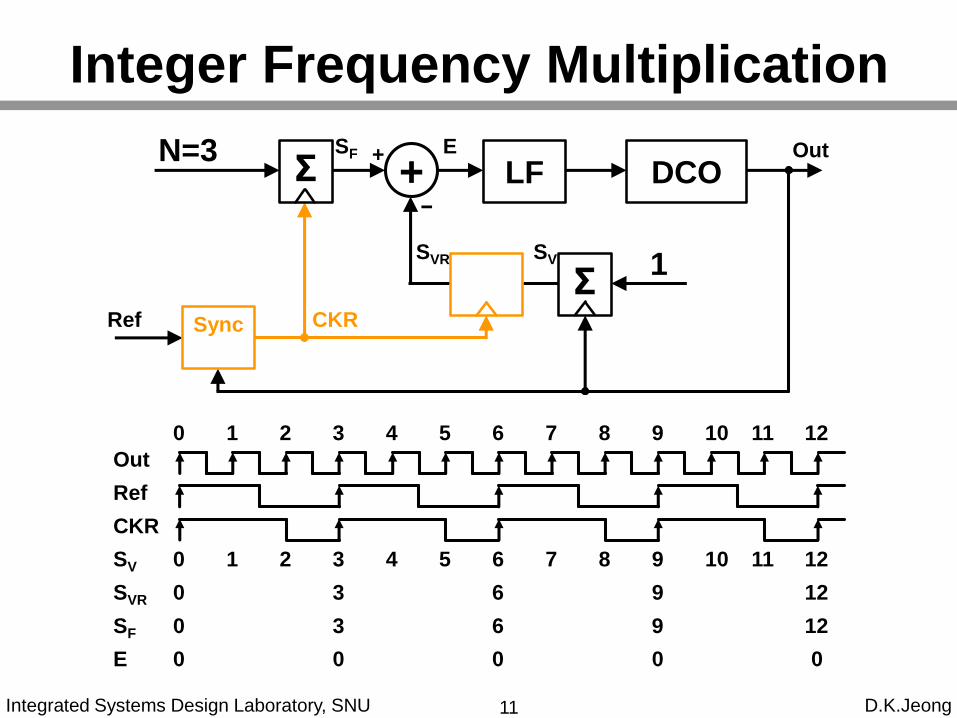
Integrated Systems Design Laboratory, SNU D.K.Jeong
Out
Ref
CKR
SF
SV
SVR
E
0 1 2 3 4 5 6 7 8 9 10 11 12
0 1 2 3 4 5 6 7 8 9 10 11 12
0 3 9 12
0
0 0
6
3 9 126
00 0
Integer Frequency Multiplication
ΣN=3
LF DCO
1Σ
+Out
Ref CKR
SF
SVR SV
E
Sync
+
−
11

Integrated Systems Design Laboratory, SNU D.K.Jeong
Out
Ref
CKR
SF
SV
SVR
E
0 1 2 3 4 5 6 7 8 9 10 11 12
0 1 2 3 4 5 6 7 8 9 10 11 12
2.25 4.5 11.25
0 3 5 7 9 12
0 6.75 9
-0.75 -0.5 -0.750 -0.25 0
Fractional Error
ΣN=2.25
LF DCO
1Σ
+Out
Ref CKR
SF
SVR SV
E
Sync
+
−
12

Integrated Systems Design Laboratory, SNU D.K.Jeong
Out
Ref
ε = 0.75 ε = 0.5 ε = 0.25 ε = 0.75ε = 0
Fractional Error Correction
[3] R. B. Staszewski TCASII 2005
TDCNormalization factor
−ε
ΣN=2.25
LF DCO
1Σ
+Out
Ref CKR
SF
SVR SV
E
Sync
+
−
13
Inconsistency
may occur

Integrated Systems Design Laboratory, SNU D.K.Jeong
• Introduction
• Recently Published ADPLLs
Outline
14

Integrated Systems Design Laboratory, SNU D.K.Jeong
ADPLL Example – 1 (1)
• Multipath gated ring oscillator TDC (GRO-TDC)
• Digital fractional noise cancellation
• Achieve low noise and wide bandwidth
[1] C.-M. Hsu JSSC 2008
15

Integrated Systems Design Laboratory, SNU D.K.Jeong
ADPLL Example – 1 (2)
Multipath GRO-TDC
• Deal with the quantization noise
directly in the digital domain
• Scale factor is easily computed
Digital noise cancellation
[1] C.-M. Hsu JSSC 2008
GRO-TDC
Multipath implementation
16

Integrated Systems Design Laboratory, SNU D.K.Jeong
ADPLL Example – 1 (3)
Passive DAC
• 5-bit resistor ladder & 5-bit
switch-capacitor array
• Minimize active circuitry and no
transistor bias current
• Achieve monotonic DAC output
with first-order filtering
[1] C.-M. Hsu JSSC 2008
Step 1: unit capacitor charged
Step 2: charge redistributed and filtered
17

Integrated Systems Design Laboratory, SNU D.K.Jeong
ADPLL Example – 2 (1)
• Fractional ADPLL without feedback divider([9] R. B. Staszewski TCASII 2005)
• Simplifies synthesizer core
• Requires more accurate TDC calibration to ensure
the ratio between Fout and Fref
[4] E. Temporiti JSSC 2009
18

Integrated Systems Design Laboratory, SNU D.K.Jeong
ADPLL Example – 2 (2)
• Fractional counter should meet N·Tdel=M·Tdco/2
M and N are relatively prime
• In this implementation, 21·Tdel=5·Tdco/2
[4] E. Temporiti JSSC 2009
19

Integrated Systems Design Laboratory, SNU D.K.Jeong
ADPLL Example – 2 (3)
• Fractional counter calibration
– Monitor the number of group of 5 identical bits
[4] E. Temporiti JSSC 2009
20

Integrated Systems Design Laboratory, SNU D.K.Jeong
ADPLL Example – 2 (4)
• Fractional counter mismatch correction
– Reference clock rate is doubled
– Generate pseudo random jitter injected ‘dirty edge’ only for
calibration and correction
(‘dirty edges’ are not used by the main loop)
– Monitor the histogram of fractional counter
[4] E. Temporiti JSSC 2009
21

Integrated Systems Design Laboratory, SNU D.K.Jeong
ADPLL Example – 3 (1)
• Fractional-N PLL with phase-interpolation divider
• TDC using dynamic element matching (DEM)
• Digital fractional noise cancellation (as [7])
• Phase interpolator mismatch cancellation
[5] M. Zanuso ISSCC 2010
22

Integrated Systems Design Laboratory, SNU D.K.Jeong
ADPLL Example – 3 (2)
• Division factor: Ndiv + (Npi + Nsd/216)/16
• All digital bang-bang servo loop forces multi-phases
to be equally spaced
[5] M. Zanuso ISSCC 2010
23

Integrated Systems Design Laboratory, SNU D.K.Jeong
ADPLL Example – 3 (3)
TDC using DEMPhase interpolator
mismatch cancellation
[5] M. Zanuso ISSCC 2010
24

Integrated Systems Design Laboratory, SNU D.K.Jeong
[1] C.-M. Hsu, et al., “A low-noise wide-BW 3.6-GHz digital ΔΣ fractional-N
frequency synthesizer with a noise-shaping time-to-digital converter
and quantization noise cancellation,” IEEE J. Solid-State Circuits, vol.
43, no. 12, pp. 2776-2786, Dec. 2008.
[2] R. B. Staszewski, et al., “A digitally controlled oscillator in a 90 nm
digital CMOS process for mobile phones,” IEEE J. Solid-State Circuits,
vol. 40, no. 11, pp. 2203-2211, Nov. 2005.
[3] R. B. Staszewski, et al., “Phase-domain all-digital phase-locked loop,”
IEEE Trans. Circuits and Syst. II: Express Briefs, vol. 52. no 3, pp. 159-
163, Mar. 2005.
[4] E. Temporiti, et al., “A 3 GHz fractional all-digital PLL with a 1.8 MHz
bandwidth implementing spur reduction techniques,” IEEE J. Solid-
State Circuits, vol. 44, no. 3, pp. 824-834, Mar. 2009.
[5] M. Zanuso, et al., “A 3MHz-BW 3.6GHz digital fractional-N PLL with
sub-gate-delay TDC, phase-interpolation divider, and digital mismatch
cancellation,” in IEEE ISSCC Dig. Tech. Papers, 2010, pp. 476-477
References (2)
25

ISDL Integrated Systems
Design Lab.
Noise Analysis of
All-Digital Pixel Clock Generator

ISDL
ISDL Integrated Systems
Design Lab.
Outline
ADPLL Block Diagram and Noise Sources
Output Noise
Calculation of Power Spectral Density
Verilog Simulation
Phase Noise and Jitter
RMS Jitter Calculation from Phase Noise
Verilog simulation
Simulation Guide
2

ISDL
ISDL Integrated Systems
Design Lab.
TDCDigital Loop
FilterΔΣ1 DCO DIVIDER
REF
1/N
ΔΣ2 DIVIDER
OUTFCW
Fractional-N
Φn,REF Φn,TDCq Φn,ΔΣ1 Φn,DCO + Φn,DCOq
Φn,ΔΣ2
ADPLL Block Diagram and Noise Sources
3
1
2
REF
TDC
T
t 2
REFf
j f
DCOK
jf
5 1 23
4
6
1 1( )
2 2
DCOREF REF
TDC
KT fA f
t j f jf N
( )( )
1 ( )
A fG f
A f
Open Loop Transfer function Closed Loop Transfer function

ISDL
ISDL Integrated Systems
Design Lab.
Power spectral density of output noise
Output Noise
4
, , , 1 , 2 , ,( ) ( ) ( ) ( ) ( ) ( ) ( )OUT OUT TDCq OUT DCOq OUT OUT OUT REF OUT DCOS f S f S f S f S f S f S f
2 22
2
, 2
2 1( ) 2sin ( )
12
n
OUT
REF REF
fS f G f
f f
22
2
,
2 1( ) ( )
12
TDCOUT TDCq
REF REF
tS f N G f
T f
22
2,
, 1
1 1( ) 2sin 1 ( )
12
n
DCO eff
OUT
f fS f G f
f f f
1 2 3 4 5
1
2
3
4
53
2
21/ ,
,
,1
2( ) 1 1 ( )
2
f REFREFOUT REF
sig VCXO
ffFkTS f N G f
P Q f f
3
2
21/ ,
,
,2
2( ) 1 1 1 ( )
2
f DCODCOOUT DCO
sig DCO
ffFkTS f G f
P Q f f
22
2,
,
1 1( ) sinc 1 ( )
12
DCO eff
OUT DCOq
f fS f G f
f f f
6
6
FDIVIDER
DCO dither
Q, DCO
Q, TDC
REF
DCO

ISDL
ISDL Integrated Systems
Design Lab.
-300.00
-250.00
-200.00
-150.00
-100.00
-50.00
0.00
1.E+00 1.E+01 1.E+02 1.E+03 1.E+04 1.E+05 1.E+06 1.E+07 1.E+08
Sout,TDC
Sout,q
Sout,ΣΔ1
Sout,ΣΔ2
Sout,REF
Sout,DCO
Sout,TOTAL
Plot of Power spectral density of output noise
Output Noise
5
fBW
1
4
3
5
6
, , , 1 , 2 , ,( ) ( ) ( ) ( ) ( ) ( ) ( )OUT OUT TDCq OUT DCOq OUT OUT OUT REF OUT DCOS f S f S f S f S f S f S f
1 2 3 4 5 6
2
Sφout,total
In this case, DCO quantization noise is dominant !!

ISDL
ISDL Integrated Systems
Design Lab.
Phase Noise and Jitter
6
C
PERf
tJ
2
)(
( )
2 10
0
1 1( ) 2 10
2 2
L f
RMS
C C
J t dff f
10
)(
2
2
210)(
4)(
4)(
fL
n
ft fSA
dtetnA
fS
))2
)((2sin())(2sin()(
C
CCf
ttfAttfAtC
RMS Jitter calculation from phase noise
0
10
)(
0 20
2 102)(4
2)(2)( dfdffSA
dffSt
fL
n
)(2
)( tA
tn )(4
)()(2
2 fSA
dtetnfS ft
n

ISDL
ISDL Integrated Systems
Design Lab.
Phase Noise and Jitter
Verilog simulation (calculation and simulation result comparison)
7
SimulationIntegral of RMS jitter, 3.7717ps
Relative RMS jitter with frequency
1 – Jitter from TDC quantization
noise
2 – Jitter from divider DSM noise
3 – Jitter from DCO DSM noise
RMS jitter
Calculation : 3.7717ps
Simulation : 3.6343ps
3
1
2
RMS Jitter of calculation and that
of verilog simulation are almost
same!