Embed Size (px)
Citation preview
TMPM3H Group(2)
Exception
2018-07-31 1 / 99 Rev. 2.0
© 2017-2018 Toshiba Electronic Devices & Storage Corporation
2018-07
32-Bit RISC Microcontroller
TMPM3H Group(2)
Reference Manual Exception
(EXCEPT-M3H(2))
Revision 2.0
TMPM3H Group(2)
Exception
2018-07-31 2 / 99 Rev. 2.0
Contents Preface ................................................................................................................................................................. 5
Related document ..................................................................................................................................................... 5
Conventions ............................................................................................................................................................ 6
Terms and Abbreviations .......................................................................................................................................... 8
1. Outlines ......................................................................................................................................................... 9
1.1. Exception Types ................................................................................................................................................ 9
1.2. Exception Handling Flowchart ......................................................................................................................... 10 1.2.1. Exception Request and Detection .............................................................................................................................. 11 1.2.2. Exception Handling and Branch to Interrupt Service Routine (Pre-emption) .............................................................. 13 1.2.3. Executing an ISR ........................................................................................................................................................ 14 1.2.4. Exception Exit ............................................................................................................................................................. 15
2. Reset Exception .......................................................................................................................................... 16
3. SysTick ........................................................................................................................................................ 17
4. Interrupts ..................................................................................................................................................... 17
4.1. Non-Maskable Interrupt (NMI) ......................................................................................................................... 17
4.2. Maskable Interrupt ........................................................................................................................................... 17
4.3. Interrupt Request ............................................................................................................................................. 18 4.3.1. Interrupt Route............................................................................................................................................................ 18 4.3.2. Interrupt Request Generation ..................................................................................................................................... 21 4.3.3. Monitor of the Interrupt Request ................................................................................................................................. 21 4.3.4. Transmission of Interrupt Request .............................................................................................................................. 21 4.3.5. Precautions When Using External Interrupt Pins ........................................................................................................ 21
4.4. List of Interrupt Sources ................................................................................................................................... 22 4.4.1. About joint interruption ................................................................................................................................................ 29
4.5. interrupt detection level .................................................................................................................................... 32 4.5.1. Precautions When Releasing the Low Power Consumption Mode ............................................................................. 32
4.6. Interrupt Handling ............................................................................................................................................ 33 4.6.1. Flowchart .................................................................................................................................................................... 33 4.6.2. Preparation ................................................................................................................................................................. 34
4.6.3. Detection (INTIF) ........................................................................................................................................................ 36
4.6.4. Detection (CPU) ......................................................................................................................................................... 36 4.6.5. CPU Processing ......................................................................................................................................................... 36 4.6.6. Interrupt Service Routine (ISR) (Clearing an interrupt Source) .................................................................................. 37
5. Exception/ Interrupt-Related Registers ....................................................................................................... 38
5.1. Register List ..................................................................................................................................................... 38
5.2. Interrupt Control Registers A ........................................................................................................................... 44 5.2.1. [IANIC00] (Non-Maskable Interrupt A Control Register 00) ........................................................................................ 44 5.2.2. [IAIMC00 to 03,16 to 17] (Interrupt A Mode Control Register n) ................................................................................. 44
5.3. Interrupt Control Registers B ........................................................................................................................... 46 5.3.1. [IBNIC00] (Non-Maskable Interrupt B Control Register 00) ........................................................................................ 46

TMPM3H Group(2)
Exception
2018-07-31 3 / 99 Rev. 2.0
5.3.2. [IBIMC000 to 065, 066 to 093, 094] (Interrupt B Mode Control Register n) ................................................................ 46 5.4. Reset Flag Registers ....................................................................................................................................... 48
5.4.1. [RLMRSTFLG0] (Reset Flag Register 0) .................................................................................................................... 48 5.4.2. [RLMRSTFLG1] (Reset Flag Register 1) .................................................................................................................... 49
5.5. Interrupt Monitor Registers .............................................................................................................................. 50 5.5.1. [IMNFLGNMI] (Non-Maskable Interrupt Monitor Flag Register).................................................................................. 50 5.5.2. [IMNFLG1] (Interrupt Monitor Flag Register 1) ........................................................................................................... 50 5.5.3. [IMNFLG3] (Interrupt Monitor Flag Register 3) ........................................................................................................... 51 5.5.4. [IMNFLG4] (Interrupt Monitor Flag Register 4) ........................................................................................................... 53 5.5.5. [IMNFLG5] (Interrupt Monitor Flag Register 5) ........................................................................................................... 55
5.6. NVIC Registers ................................................................................................................................................ 57 5.6.1. SysTick Control and Status Register .......................................................................................................................... 57 5.6.2. SysTick Reload Value Register .................................................................................................................................. 57 5.6.3. SysTick Current Value Register .................................................................................................................................. 57 5.6.4. SysTick Calibration Value Register ............................................................................................................................ 58 5.6.5. Interrupt Control Registers ......................................................................................................................................... 59
5.6.5.1. Interrupt Set-Enable Register ........................................................................................................................................ 59 5.6.5.2. Interrupt Clear-Enable Register ..................................................................................................................................... 65 5.6.5.3. Interrupt Set-Pending Register ...................................................................................................................................... 71 5.6.5.4. Interrupt Clear-Pending Register ................................................................................................................................... 77
5.6.6. Interrupt Priority Register ............................................................................................................................................ 83 5.6.7. Vector Table Offset Register ...................................................................................................................................... 84 5.6.8. Application Interrupt and Reset Control Register ....................................................................................................... 85 5.6.9. System Handler Priority Register ................................................................................................................................ 86 5.6.10. System Handler Control and State Register ............................................................................................................. 87
6. List of Interrupt Sources for Each Product .................................................................................................. 88
6.1. TMPM3HQ,TMPM3HP,TMPM3HN,TMPM3HM,TMPM3HL ............................................................................ 88
7. Revision History .......................................................................................................................................... 98
RESTRICTIONS ON PRODUCT USE ............................................................................................................... 99

TMPM3H Group(2)
Exception
2018-07-31 4 / 99 Rev. 2.0
List of Figures Figure 4.1 Interruption transfer route Diagram ........................................................................................ 19
List of Tables Table 1.1 Exception Types and Priority ................................................................................................... 11 Table 1.2 Priority grouping setting ........................................................................................................... 12 Table 4.1 Explanation of each interruption transfer route ........................................................................ 20 Table 4.2 List of Interrupt Sources (Non-Maskable Interrupt) ................................................................. 22 Table 4.3 List of Interrupt Sources (Interrupt Control Register A) ........................................................... 22 Table 4.4 List of Interrupt Sources (Interrupt Control Register B) (1/6) ................................................ 23 Table 4.5 List of Interrupt Sources (Interrupt Control Register B) (2/6) ................................................ 24 Table 4.6 List of Interrupt Sources (Interrupt Control Register B) (3/6) ................................................ 25 Table 4.7 List of Interrupt Sources (Interrupt Control Register B) (4/6) ................................................ 26 Table 4.8 List of Interrupt Sources (Interrupt Control Register B) (5/6) ................................................ 27 Table 4.9 List of Interrupt Sources (Interrupt Control Register B) (6/6) ................................................ 28 Table 4.10 Joint interruption Connection list (1) ...................................................................................... 29 Table 4.11 Joint interruption Connection list (2) ...................................................................................... 30 Table 4.12 Joint interruption Connection list (3) ...................................................................................... 31 Table 6.1 List of interrupt request (1/6) .................................................................................................... 88 Table 6.2 List of interrupt request (2/6) .................................................................................................... 89 Table 6.3 List of interrupt request (3/6) .................................................................................................... 90 Table 6.4 List of interrupt request (4/6) .................................................................................................... 91 Table 6.5 List of interrupt request (5/6) .................................................................................................... 92 Table 6.6 List of interrupt request (6/6) .................................................................................................... 93 Table 6.7 Interrupt Number 158 (1/2) ...................................................................................................... 94 Table 6.8 Interrupt Number 158 (2/2) ...................................................................................................... 95 Table 6.9 Interrupt Number 160 (1/2) ...................................................................................................... 96 Table 6.10 Interrupt Number 160 (2/2) .................................................................................................... 97 Table 7.1 Revision History ....................................................................................................................... 98
TMPM3H Group(2)
Exception
2018-07-31 5 / 99 Rev. 2.0
Preface Related document
Document name
Power Supply and Reset Operation
Oscillation Frequency Detector
Clock Selective Watchdog Timer
Voltage Detection Circuit
Clock Control and Operation Mode
Arm® documentation set for the Arm Cortex®-M3 processor

TMPM3H Group(2)
Exception
2018-07-31 6 / 99 Rev. 2.0
Conventions ● Numeric formats follow the rules as shown below:
Hexadecimal: 0xABC Decimal: 123 or 0d123 – Only when it needs to be explicitly shown that they are decimal numbers. Binary: 0b111 – It is possible to omit the “0b” when the number of bit can be distinctly understood from a sentence.
● “_N” is added to the end of signal names to indicate low active signals. ● It is called “assert” that a signal moves to its active level, “deassert” to its inactive level. ● When two or more signal names are referred, they are described like as [m: n].
Example: S[3: 0] shows four signal names S3, S2, S1 and S0 together. ● The characters surrounded by [ ] defines the register.
Example: [ABCD] ● “n” substitutes suffix number of two or more same kind of registers, fields, and bit names.
Example: [XYZ1], [XYZ2], [XYZ3] [XYZn] ● "x" substitutes suffix number or character of units and channels in the Register List.
In case of unit, “x” means A, B, and C . . . Example: [ADACR0], [ADBCR0], [ADCCR0] [ADxCR0] In case of channel, “x” means 0, 1, and 2 . . . Example: [T32A0RUNA], [T32A1RUNA], [T32A2RUNA] [T32AxRUNA]
● The bit range of a register is written like as [m: n]. Example: Bit[3: 0] expresses the range of bit 3 to 0.
● The configuration value of a register is expressed by either the hexadecimal number or the binary number. Example: [ABCD]<EFG> = 0x01 (hexadecimal), [XYZn]<VW> = 1 (binary)
● Word and Byte represent the following bit length. Byte: 8 bits Half word: 16 bits Word: 32 bits Double word: 64 bits
● Properties of each bit in a register are expressed as follows: R: Read only W: Write only R/W: Read and Write are possible
● Unless otherwise specified, register access supports only word access. ● The register defined as reserved must not be rewritten. Moreover, do not use the read value. ● The value read from the bit having default value of "-" is unknown. ● When a register containing both of writable bits and read-only bits is written, read-only bits should be
written with their default value, In the cases that default is “-“, follow the definition of each register. ● Reserved bits of the Write-only register should be written with their default value. In the cases that default is
“-“, follow the definition of each register. ● Do not use read-modified-write processing to the register of a definition which is different by writing and
read out.
TMPM3H Group(2)
Exception
2018-07-31 7 / 99 Rev. 2.0
The Flash memory uses the Super Flash® technology under license from Silicon Storage Technology, Inc. Super Flash® is registered trademark of Silicon Storage Technology, Inc. All other company names, product names, and service names mentioned herein may be trademarks of their respective companies.
*********************************************************************************************************************** Arm, Cortex and Thumb are registered trademarks of Arm Limited (or its subsidiaries) in the US and/or elsewhere. All rights reserved. ***********************************************************************************************************************
TMPM3H Group(2)
Exception
2018-07-31 8 / 99 Rev. 2.0
Terms and Abbreviations Some of abbreviations used in this document are as follows:
ADC Analog to Digital Converter A-ENC Advanced Encoder input Circuit A-PMD Advanced Programmable Motor Control Circuit DAC Digital to Analog Converter DMAC Direct Memory Access Controller DNF Digital Noise Filter IA Interrupt control register A IB Interrupt control register B IMCxx Interrupt Mode Control xx IMNFLGNMI Interrupt Monitor Flag NMI IMNFLGx Interrupt Monitor Flag x INT Interrupt INTIF Interrupt Interface Logic ISR Interrupt Service Routine I2C Inter-Integrated Circuit I2CS I2C wake-up circuit from Stand-by mode LVD Voltage Detection Circuit NICxx Non-Maskable Interrupt Control xx NVIC Nested Vectored Interrupt Controller OFD Oscillation Frequency Detector RLMRSTFLGx RLM Reset Flag x RMC Remote Control Signal preprocessor RTC Real Time Clock SIWDT Clock Selective Watchdog Timer TRGSEL Trigger Selection circuit TRM Trimming Circuit TSPI Toshiba Serial Peripheral Interface T32A 32-bit Timer Event Counter UART Universal Asynchronous Receiver Transmitter
TMPM3H Group(2)
Exception
2018-07-31 9 / 99 Rev. 2.0
Exceptions have close relation to the CPU core. Refer to “Arm documentation set for the Arm® Cortex®-M3 processor” if needed.
1. Outlines
Exceptions require CPU to suspend the currently executing process, and to start another process. There are two types of exceptions: those that are generated when some error condition occurs or when an
instruction to generate an exception is executed; and those that are generated by hardware, such as an interrupt request signal from an external pin or peripheral function.
All exceptions are handled by the Nested Vectored Interrupt Controller (NVIC) in the CPU according to the
respective priority levels. When an exception occurs, the CPU stores the current state to the stack and branches to the corresponding interrupt service routine (ISR). Upon completion of the ISR, the information stored to the stack is automatically restored.
1.1. Exception Types The following types of exceptions exist in the Cortex-M3. For detailed descriptions on each exception, refer to “Arm documentation set for the Arm Cortex-M3
processor”.
● Reset ● Non-Maskable Interrupt(NMI) ● Hard Fault ● Memory Management ● Bus Fault ● Usage Fault ● SVCall (Supervisor Call) ● Debug Monitor ● PendSV ● SysTick ● External Interrupt

TMPM3H Group(2)
Exception
2018-07-31 10 / 99 Rev. 2.0
1.2. Exception Handling Flowchart The following shows how an exception/interrupt is handled. In the following descriptions exception handling by
hardware and that by software are explained. Each step is described later in this reference manual.
Process
Description
See
Detection by INTIF/CPU
The INTIF/CPU detects the exception request.
Section 1.2.1
Handling by CPU
The CPU handles the exception request.
Section 1.2.2
Branch to ISR
The CPU branches to the corresponding interrupt service routine (ISR).
Section 1.2.2
Execution of ISR
Necessary processing is executed
Section 1.2.3
Return from exception
The CPU branches to another ISR or returns to the previous program. Section 1.2.4

TMPM3H Group(2)
Exception
2018-07-31 11 / 99 Rev. 2.0
1.2.1. Exception Request and Detection
(1) Exception Occurrence Exception sources include instruction execution by the CPU, memory accesses, and interrupt requests
from external interrupt pins or peripheral functions. An exception by the instruction execution occurs when the CPU executes an instruction that causes an
exception or when an error condition occurs during instruction execution. An exception also occurs by an instruction fetch from the Execute Never (XN) region or an access
violation to the Fault region. The request of the exception by the external interruption terminal or the peripheral function occurs by
each functional factor. Regarding to interruption which connected via INTIF, the setup of the Interrupt Control Register is needed. For details, refer to the chapter, “4 Interrupts”.
(2) Exception Detection
If multiple exceptions occur simultaneously, the CPU takes the exception with the highest priority. The priority of exceptions are below. “Configurable” means that you can assign a priority level to that
exception. Memory Management, Bus Fault and Usage Fault exceptions can be enabled or disabled. If a disabled exception occurs, it is handled as Hard Fault.
Table 1.1 Exception Types and Priority
Exception Type Priority Description Offset
Reset -3(highest) Reset pin, SIWDT, POR, OFD, LVD, STOP2 releasing, SYSRESETREQ, LOCKUP signal 0x00
Non-Maskable Interrupt -2 SIWDT, LVD 0x08
Hard Fault -1 Fault that cannot activate because a higher-priority fault is being handled or it is disabled 0x0C
Memory Management Configurable Exception from the Memory Protection Unit (MPU)
Instruction fetch from the Execute Never (XN) region 0x10
Bus Fault Configurable Access violation to the Hard Fault region of the memory map 0x14
Usage Fault Configurable Undefined instruction execution or other faults related to instruction execution 0x18
Reserved - 0x1C to 0x28
SVCall Configurable System service call with SVC instruction 0x2C
Debug Monitor Configurable Debug monitor when the CPU is not faulting 0x30
Reserved - 0x34
PendSV Configurable Pending system service request 0x38
SysTick Configurable Notification from system timer 0x3C
External Interrupt Configurable External interrupt pin or peripheral function (Note) 0x40
Note: External interrupts have different sources and numbers in each product. For details, see “4.4 List of Interrupt Sources”.
TMPM3H Group(2)
Exception
2018-07-31 12 / 99 Rev. 2.0
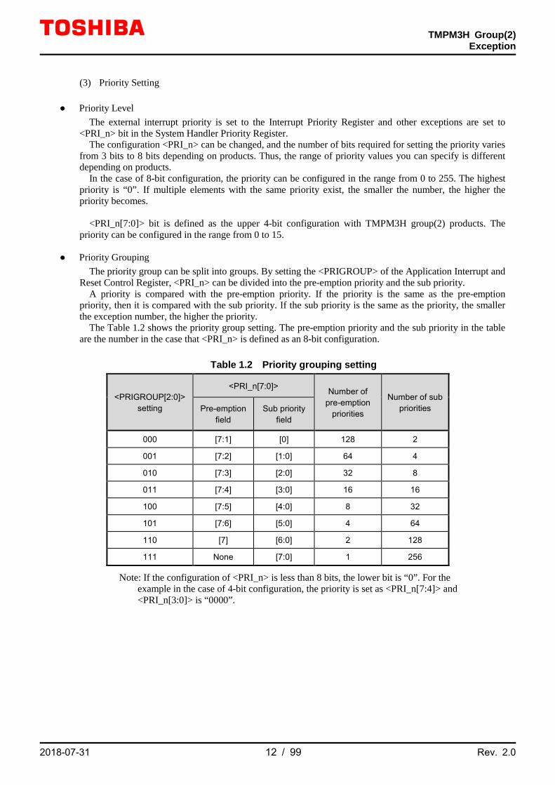
(3) Priority Setting
● Priority Level
The external interrupt priority is set to the Interrupt Priority Register and other exceptions are set to <PRI_n> bit in the System Handler Priority Register.
The configuration <PRI_n> can be changed, and the number of bits required for setting the priority varies from 3 bits to 8 bits depending on products. Thus, the range of priority values you can specify is different depending on products.
In the case of 8-bit configuration, the priority can be configured in the range from 0 to 255. The highest priority is “0”. If multiple elements with the same priority exist, the smaller the number, the higher the priority becomes.
<PRI_n[7:0]> bit is defined as the upper 4-bit configuration with TMPM3H group(2) products. The
priority can be configured in the range from 0 to 15.
● Priority Grouping The priority group can be split into groups. By setting the <PRIGROUP> of the Application Interrupt and
Reset Control Register, <PRI_n> can be divided into the pre-emption priority and the sub priority. A priority is compared with the pre-emption priority. If the priority is the same as the pre-emption
priority, then it is compared with the sub priority. If the sub priority is the same as the priority, the smaller the exception number, the higher the priority.
The Table 1.2 shows the priority group setting. The pre-emption priority and the sub priority in the table are the number in the case that <PRI_n> is defined as an 8-bit configuration.
Table 1.2 Priority grouping setting
<PRIGROUP[2:0]> setting
<PRI_n[7:0]> Number of pre-emption
priorities
Number of sub priorities Pre-emption
field Sub priority
field
000 [7:1] [0] 128 2
001 [7:2] [1:0] 64 4
010 [7:3] [2:0] 32 8
011 [7:4] [3:0] 16 16
100 [7:5] [4:0] 8 32
101 [7:6] [5:0] 4 64
110 [7] [6:0] 2 128
111 None [7:0] 1 256
Note: If the configuration of <PRI_n> is less than 8 bits, the lower bit is “0”. For the example in the case of 4-bit configuration, the priority is set as <PRI_n[7:4]> and <PRI_n[3:0]> is “0000”.
TMPM3H Group(2)
Exception
2018-07-31 13 / 99 Rev. 2.0
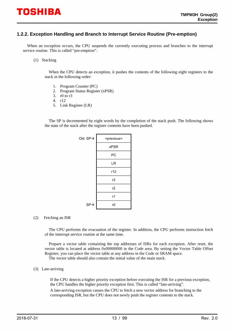
1.2.2. Exception Handling and Branch to Interrupt Service Routine (Pre-emption)
When an exception occurs, the CPU suspends the currently executing process and branches to the interrupt service routine. This is called “pre-emption”.
(1) Stacking
When the CPU detects an exception, it pushes the contents of the following eight registers to the
stack in the following order:
1. Program Counter (PC) 2. Program Status Register (xPSR) 3. r0 to r3 4. r12 5. Link Register (LR)
The SP is decremented by eight words by the completion of the stack push. The following shows the state of the stack after the register contents have been pushed.
Old SP <previous>
xPSR
PC
LR
r12
r3
r2
r1
SP r0
(2) Fetching an ISR
The CPU performs the evacuation of the register. In addition, the CPU performs instruction fetch
of the interrupt service routine at the same time. Prepare a vector table containing the top addresses of ISRs for each exception. After reset, the
vector table is located at address 0x00000000 in the Code area. By setting the Vector Table Offset Register, you can place the vector table at any address in the Code or SRAM space.
The vector table should also contain the initial value of the main stack.
(3) Late-arriving
If the CPU detects a higher priority exception before executing the ISR for a previous exception, the CPU handles the higher priority exception first. This is called “late-arriving”. A late-arriving exception causes the CPU to fetch a new vector address for branching to the corresponding ISR, but the CPU does not newly push the register contents to the stack.
TMPM3H Group(2)
Exception
2018-07-31 14 / 99 Rev. 2.0
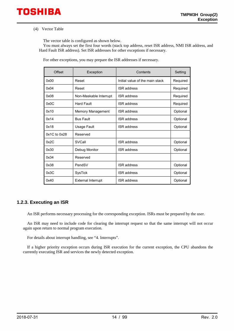
(4) Vector Table The vector table is configured as shown below. You must always set the first four words (stack top address, reset ISR address, NMI ISR address, and
Hard Fault ISR address). Set ISR addresses for other exceptions if necessary.
For other exceptions, you may prepare the ISR addresses if necessary.
Offset Exception Contents Setting
0x00 Reset Initial value of the main stack Required
0x04 Reset ISR address Required
0x08 Non-Maskable Interrupt ISR address Required
0x0C Hard Fault ISR address Required
0x10 Memory Management ISR address Optional
0x14 Bus Fault ISR address Optional
0x18 Usage Fault ISR address Optional
0x1C to 0x28 Reserved
0x2C SVCall ISR address Optional
0x30 Debug Monitor ISR address Optional
0x34 Reserved
0x38 PendSV ISR address Optional
0x3C SysTick ISR address Optional
0x40 External Interrupt ISR address Optional
1.2.3. Executing an ISR
An ISR performs necessary processing for the corresponding exception. ISRs must be prepared by the user. An ISR may need to include code for clearing the interrupt request so that the same interrupt will not occur
again upon return to normal program execution. For details about interrupt handling, see “4. Interrupts”. If a higher priority exception occurs during ISR execution for the current exception, the CPU abandons the
currently executing ISR and services the newly detected exception.
TMPM3H Group(2)
Exception
2018-07-31 15 / 99 Rev. 2.0
1.2.4. Exception Exit
(1) Execution after Returning from ISR
When returning from an ISR, the CPU takes one of the following actions: ▪ Tail-chaining
If a pending exception exists and there are no stacked exceptions or the pending exception has higher priority than all stacked exceptions, the CPU returns to the ISR of the pending exception.
In this case, the CPU skips the pop of eight registers and push of eight registers when exiting one ISR and entering another. This is called “tail-chaining”.
▪ Returning to the last stacked ISR If there are no pending exceptions or if the highest priority stacked exception is of higher priority
than the highest priority pending exception, the CPU returns to the last stacked ISR.
▪ Returning to the previous program If there are no pending or stacked exceptions, the CPU returns to the previous program.
(2) Exception Exit Sequence
When returning from an ISR, the CPU performs the following operations:
▪ Pop eight registers
Pop eight registers (PC, xPSR, r0 to r3, r12, and LR) from the stack and adjust the SP.
▪ Lord current active interrupt number Loads the current active interrupt number from the stacked xPSR. The CPU uses this to track
which interrupt to return to.
▪ Select SP If returning to an exception (Handler Mode), SP is SP_main. If returning to Thread Mode, SP can
be SP_main or SP_process.

TMPM3H Group(2)
Exception
2018-07-31 16 / 99 Rev. 2.0
2. Reset Exception Reset exceptions are generated from the following seven sources. Use the [RLMRSTFLGn] of the Reset Flag Register to identify the source of a reset.
▪ Reset exception by external reset pin A reset exception occurs when an external reset pin changes from “Low" to “High”.
▪ Reset exception by POR
A reset exception occurs by POR. For details, refer to “Power Supply and Reset Operation” of reference manual.
▪ Reset exception by OFD
A reset exception occurs by OFD. For details, refer to “Oscillation Frequency Detector” of reference manual.
▪ Reset exception by SIWDT
The SIWDT has a reset generating feature. For details, refer to “Clock Selective Watchdog Timer” of reference manual.
▪ Reset exception by LVD
The LVD has a reset generating feature. For details, refer to “Voltage Detection Circuit” of reference manual.
▪ Reset exception by STOP2 mode release
A reset exception occurs when releasing STOP2 mode. For details, refer to “Clock Control and Operation Mode” reference manual.
▪ Reset exception by <SYSRESETREQ>
A reset can be generated by setting the <SYSRESETREQ> bit in the NVIC's Application Interrupt and Reset Control Register.
▪ Reset exception by LOCKUP signal A reset can be generated by the LOCKUP signal which can be output from the CPU when the
un-recoverable interrupt occurs. For details on the LOCKUP signal, please refer to “Arm documentation set for the Arm Cortex-M3 processor”.

TMPM3H Group(2)
Exception
2018-07-31 17 / 99 Rev. 2.0
3. SysTick SysTick provides interrupt features using the CPU's system timer. When you set a value in the SysTick Reload Value Register and enable the SysTick features in the SysTick
Control and Status Register, the counter loads with the value set in the Reload Value Register and begins counting down. When the counter reaches “0”, a SysTick exception occurs. You may be pending exceptions and use a flag to know when the timer reaches “0”.
4. Interrupts This section explains the route from which a factor and an interrupt request are transmitted, and a required
setup.
4.1. Non-Maskable Interrupt (NMI) Non-Maskable interrupts are generated from the following two sources.
▪ Non-Maskable interrupt by SIWDT The SIWDT has a Non-Maskable interrupt generating feature.
▪ Non-Maskable interrupt by LVD
The LVD has a Non-Maskable interrupt generating feature.
4.2. Maskable Interrupt Please refer to Interrupt Control Register A/ Interrupt Control Register B of the "4.4. List of Interrupt Sources"
for the factors of the maskable interrupts.
TMPM3H Group(2)
Exception
2018-07-31 18 / 99 Rev. 2.0
4.3. Interrupt Request The CPU is notified of interrupt requests by the interrupt signal from each interrupt source. It sets priority on
interrupts and handles an interrupt request with the highest priority.
4.3.1. Interrupt Route The interrupt is available for the cancellation from a low power consumption mode, and a route varies
according to a factor. Figure 4.1 shows the interruption transfer route Diagram and Table 4.1 shows the explanation of each
interruption transfer route.
● The interrupt that is releasable from IDLE, STOP1, STOP2 mode Interruption which can be canceled of IDLE, STOP1, and the STOP2 mode is controlled by the
Interrupt Control Register A in INTIF via INTIF, and is notified to CPU. (Route A, B, C)
● The interrupt that is releasable from IDLE, STOP1 mode Interruption which can be canceled of IDLE and the STOP1 mode is controlled by the Interrupt
Control Register B in INTIF via INTIF, and is notified to CPU. (Route D, E, F)
● The interrupt that is releasable from IDLE mode Although some factors of interruption which can be canceled of IDLE mode are controlled by the
Interrupt Control Register B via INTIF (Route G), other factors are notified to CPU directly (Route H) not passing through INTIF.
When the interrupt factor that went by way of an interrupt regardless of low power consumption mode
cancellation is used, setting of Interrupt Control Register A or B is necessary. Please refer to the chapter of "The release source of a Low Power Consumption mode" of a reference manual
"Clock Control and Operation Mode" for the details of a low power consumption mode release factor.

TMPM3H Group(2)
Exception
2018-07-31 19 / 99 Rev. 2.0
Figure 4.1 Interruption transfer route Diagram
External Interrupt
Pin
Peripheral Function
INTIF
Interruption detection level selection logic
Interrupt detection
logic
1
0
CPU
Peripheral Function
Port
Route A
Interrupt Control Register A
[IANIC00]<INTNFLG><INTNCLR>
Interrupt detection
logic
[IAIMCxx]<INTPFLG><INTPCLR><INTNFLG><INTNCLR>
[IAIMCxx]<INTEN>
[IAIMCxx]<INTMODE[2:0]>
Route B
Peripheral Function
Interrupt detection
logic
Route D
[IBNIC00]<INTPFLG><INTPCLR>
Interrupt detection
logic
[IBIMCxxx]<INTPFLG><INTPCLR>
Interruption detection level selection logic
10
Interrupt detection
logic
[IBIMCxxx]<INTPFLG><INTPCLR><INTNFLG><INTNCLR>
[IBIMCxxx]<INTEN>
[IBIMCxxx]<INTMODE[2:0]>
Peripheral Function
Route F
Interrupt Control Register B
1
0
Interrupt detection
logic
[IBIMCxxx]<INTPFLG><INTPCLR>
[IBIMCxxx]<INTEN>
Peripheral Function
Route G
Peripheral Function
Route H
Route C
Route E
IDLESTOP1STOP2release sources
IDLESTOP1release sources
IDLErelease sources
NVIC Register/ Interrupt mask
Register
1
0
Interrupt detection
logic
[IAIMCxx]<INTPFLG><INTPCLR><INTNFLG><INTNCLR>
[IAIMCxx]<INTEN>
Interrupt Monitor Registers [IMNFLGNMI] [IMNFLG1,3,4,5]
TMPM3H Group(2)
Exception
2018-07-31 20 / 99 Rev. 2.0
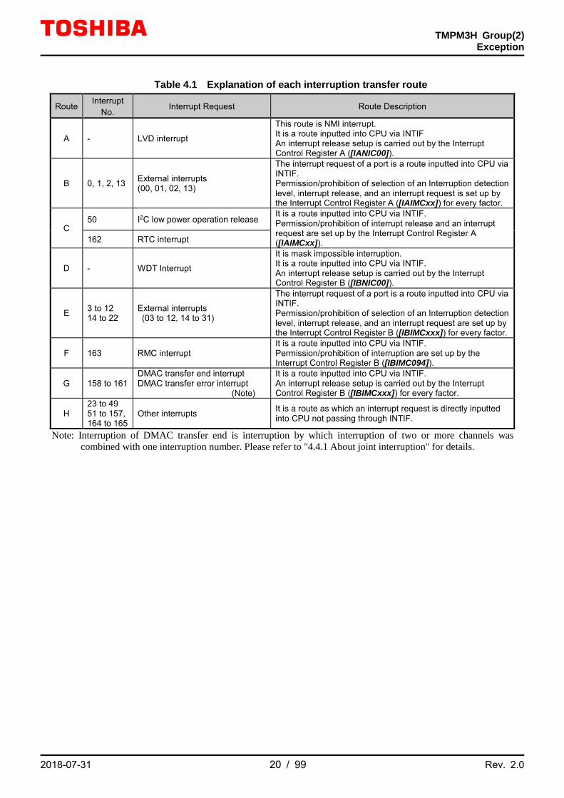
Table 4.1 Explanation of each interruption transfer route
Route Interrupt
No. Interrupt Request Route Description
A - LVD interrupt
This route is NMI interrupt. It is a route inputted into CPU via INTIF An interrupt release setup is carried out by the Interrupt Control Register A ([IANIC00]).
B 0, 1, 2, 13 External interrupts (00, 01, 02, 13)
The interrupt request of a port is a route inputted into CPU via INTIF. Permission/prohibition of selection of an Interruption detection level, interrupt release, and an interrupt request is set up by the Interrupt Control Register A ([IAIMCxx]) for every factor.
C 50 I2C low power operation release
It is a route inputted into CPU via INTIF. Permission/prohibition of interrupt release and an interrupt request are set up by the Interrupt Control Register A ([IAIMCxx]). 162 RTC interrupt
D - WDT Interrupt
It is mask impossible interruption. It is a route inputted into CPU via INTIF. An interrupt release setup is carried out by the Interrupt Control Register B ([IBNIC00]).
E 3 to 12 14 to 22
External interrupts (03 to 12, 14 to 31)
The interrupt request of a port is a route inputted into CPU via INTIF. Permission/prohibition of selection of an Interruption detection level, interrupt release, and an interrupt request are set up by the Interrupt Control Register B ([IBIMCxxx]) for every factor.
F 163 RMC interrupt It is a route inputted into CPU via INTIF. Permission/prohibition of interruption are set up by the Interrupt Control Register B ([IBIMC094]).
G 158 to 161 DMAC transfer end interrupt DMAC transfer error interrupt (Note)
It is a route inputted into CPU via INTIF. An interrupt release setup is carried out by the Interrupt Control Register B ([IBIMCxxx]) for every factor.
H 23 to 49 51 to 157, 164 to 165
Other interrupts It is a route as which an interrupt request is directly inputted into CPU not passing through INTIF.
Note: Interruption of DMAC transfer end is interruption by which interruption of two or more channels was combined with one interruption number. Please refer to "4.4.1 About joint interruption" for details.

TMPM3H Group(2)
Exception
2018-07-31 21 / 99 Rev. 2.0
4.3.2. Interrupt Request Generation An interrupt request is generated from an external interrupt pin or peripheral function which are assigned as
interrupt request sources, or by setting the relevant bit of NVIC's Interrupt Set-Pending Register for interrupt request source.
● Interrupt from external interrupt pin
Set the port control register so that the external pin can perform as an interrupt function pin.
● Interrupt from peripheral function Set the peripheral function to make it possible to output interrupt requests. See the chapter of each peripheral function for details.
● By setting Interrupt Set-Pending Register (forced pending) An interrupt request can be forced to be generated by setting the relevant bit of the Interrupt
Set-Pending Register of NVIC.
CPU will recognize the "High" level of the interrupt request as an interrupt.
4.3.3. Monitor of the Interrupt Request INTIF has the interruption monitor flags. It can know that the interrupt request has occurred by monitoring the
flag. If one request source is representing several interrupt requests, Interrupt Monitor Register can be used to identify the actual interrupt request source. For detail, please refer to "4.4. List of Interrupt Sources".
4.3.4. Transmission of Interrupt Request An interrupt request which is not passing through the Interrupt Control Register will be directly input to the
CPU. The interrupts connected to the CPU through INTIF, which are used as interrupt request sources for releasing the low power consumption mode, will need proper setting of the Interrupt Control Register in INTIF. An "High" level interrupt signal will be sent to the CPU, when the interrupt is used to release the low power consumption mode.
Please setup an interruption detection level and interruption enable/disable by INTIF. By the way, please be cautious about external interrupt pin as in the next section.
4.3.5. Precautions When Using External Interrupt Pins When you use external interrupt, please care about the following points so that an unexpected interrupt does not
occur. If input is disabled ([PxIE]<PxmIE>=0), inputs from external interrupt pins are "Low". When the
<INTMODE> bit of Interrupt Control Register A ([IAIMCxx]) is "Low", then input signals from the external interrupt pins are sent to the CPU as is. Since the CPU recognizes "Low" input as an interrupt, interrupts occur if corresponding interrupts are enabled by the CPU. The interrupt pins should be "High" and the inputs should be enabled. Then the interrupts should be enabled by the CPU.
TMPM3H Group(2)
Exception
2018-07-31 22 / 99 Rev. 2.0
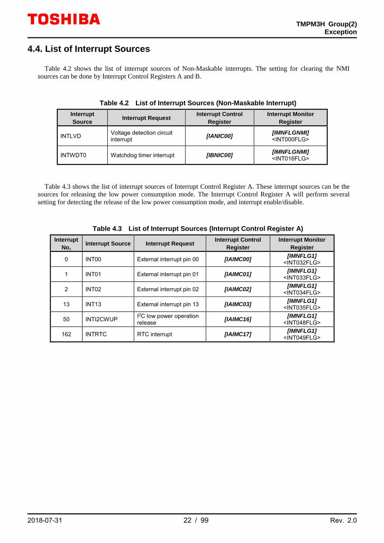
4.4. List of Interrupt Sources Table 4.2 shows the list of interrupt sources of Non-Maskable interrupts. The setting for clearing the NMI
sources can be done by Interrupt Control Registers A and B.
Table 4.2 List of Interrupt Sources (Non-Maskable Interrupt) Interrupt Source Interrupt Request Interrupt Control
Register Interrupt Monitor
Register
INTLVD Voltage detection circuit interrupt [IANIC00] [IMNFLGNMI]
<INT000FLG>
INTWDT0 Watchdog timer interrupt [IBNIC00] [IMNFLGNMI] <INT016FLG>
Table 4.3 shows the list of interrupt sources of Interrupt Control Register A. These interrupt sources can be the
sources for releasing the low power consumption mode. The Interrupt Control Register A will perform several setting for detecting the release of the low power consumption mode, and interrupt enable/disable.
Table 4.3 List of Interrupt Sources (Interrupt Control Register A) Interrupt
No, Interrupt Source Interrupt Request Interrupt Control Register
Interrupt Monitor Register
0 INT00 External interrupt pin 00 [IAIMC00] [IMNFLG1] <INT032FLG>
1 INT01 External interrupt pin 01 [IAIMC01] [IMNFLG1] <INT033FLG>
2 INT02 External interrupt pin 02 [IAIMC02] [IMNFLG1] <INT034FLG>
13 INT13 External interrupt pin 13 [IAIMC03] [IMNFLG1] <INT035FLG>
50 INTI2CWUP I2C low power operation release [IAIMC16] [IMNFLG1]
<INT048FLG>
162 INTRTC RTC interrupt [IAIMC17] [IMNFLG1] <INT049FLG>

TMPM3H Group(2)
Exception
2018-07-31 23 / 99 Rev. 2.0
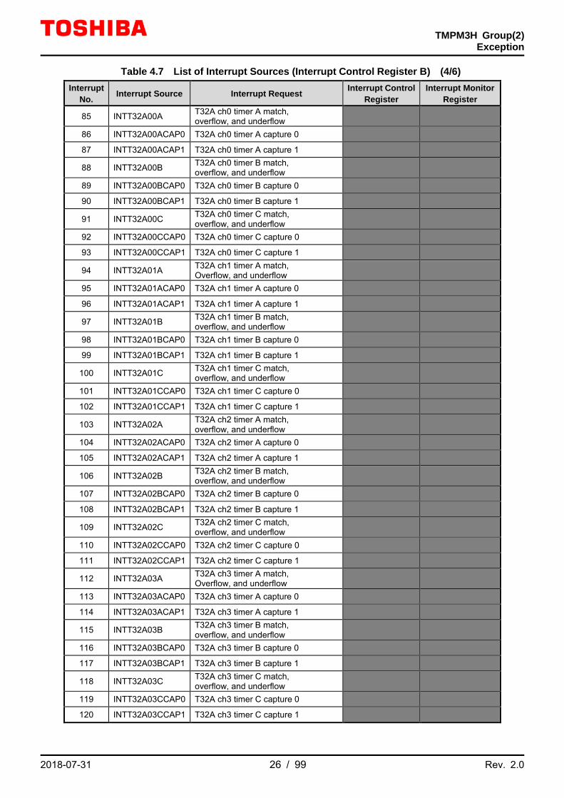
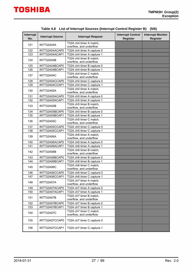
The factor list of the Interrupt Control Registers B is shown in Table 4.4 to 4.7. A part of interruption sets up
interruption permission / prohibition by the Interrupt Control Register B.
Table 4.4 List of Interrupt Sources (Interrupt Control Register B) (1/6) Interrupt
No. Interrupt Source Interrupt Request Interrupt Control
Register Interrupt Monitor
Register
3 INT03 External interrupt pin 03 [IBIMC066] [IMNFLG5] <INT162FLG>
4 INT04 External interrupt pin 04 [IBIMC067] [IMNFLG5] <INT163FLG>
5 INT05 External interrupt pin 05 [IBIMC068] [IMNFLG5] <INT164FLG>
6 INT06 External interrupt pin 06 [IBIMC069] [IMNFLG5] <INT165FLG>
7 INT07 External interrupt pin 07 [IBIMC070] [IMNFLG5] <INT166FLG>
8 INT08 External interrupt pin 08 [IBIMC071] [IMNFLG5] <INT167FLG>
9 INT09 External interrupt pin 09 [IBIMC072] [IMNFLG5] <INT168FLG>
10 INT10 External interrupt pin 10 [IBIMC073] [IMNFLG5] <INT169FLG>
11 INT11 External interrupt pin 11 [IBIMC074] [IMNFLG5] <INT170FLG>
12 INT12 External interrupt pin 12 [IBIMC075] [IMNFLG5] <INT171FLG>
14 INT14 External interrupt pin 14 [IBIMC076] [IMNFLG5] <INT172FLG>
15 INT15 External interrupt pin 15 [IBIMC077] [IMNFLG5] <INT173FLG>
16 INT16 External interrupt pin 16 [IBIMC078] [IMNFLG5] <INT174FLG>
17 INT17_18 External interrupt pin 17 [IBIMC079] [IMNFLG5]
<INT175FLG>
External interrupt pin 18 [IBIMC080] [IMNFLG5] <INT176FLG>
18 INT19_22
External interrupt pin 19 [IBIMC081] [IMNFLG5] <INT177FLG>
External interrupt pin 20 [IBIMC082] [IMNFLG5] <INT178FLG>
External interrupt pin 21 [IBIMC083] [IMNFLG5] <INT179FLG>
External interrupt pin 22 [IBIMC084] [IMNFLG5] <INT180FLG>
19 INT23_26
External interrupt pin 23 [IBIMC085] [IMNFLG5] <INT181FLG>
External interrupt pin 24 [IBIMC086] [IMNFLG5] <INT182FLG>
External interrupt pin 25 [IBIMC087] [IMNFLG5] <INT183FLG>
External interrupt pin 26 [IBIMC088] [IMNFLG5] <INT184FLG>
20 INT27_28 External interrupt pin 27 [IBIMC089] [IMNFLG5]
<INT185FLG>
External interrupt pin 28 [IBIMC090] [IMNFLG5] <INT186FLG>
21 INT29 External interrupt pin 29 [IBIMC091] [IMNFLG5] <INT187FLG>
22 INT30_31 External interrupt pin 30 [IBIMC092] [IMNFLG5]
<INT188FLG>
External interrupt pin 31 [IBIMC093] [IMNFLG5] <INT189FLG>

TMPM3H Group(2)
Exception
2018-07-31 24 / 99 Rev. 2.0
Table 4.5 List of Interrupt Sources (Interrupt Control Register B) (2/6)
Interrupt No.
Interrupt Source Interrupt Request Interrupt Control
Register Interrupt Monitor
Register 23 INTEMG0 A-PMD ch0 EMG interrupt
24 INTOVV0 A-PMD ch0 OVV interrupt
25 INTPMD0 A-PMD ch0 PWM interrupt
26 INTENC00 Encoder ch0 interrupt 0
27 INTENC01 Encoder ch0 interrupt 1
28 INTADAPDA ADC PMD trigger program conversion complete A
29 INTADAPDB ADC PMD trigger program conversion complete B
30 INTADACP0 ADC monitor function 0 interrupt
31 INTADACP1 ADC monitor function 1 interrupt
32 INTADATRG ADC general trigger program conversion complete
33 INTADASGL ADC single program conversion complete
34 INTADACNT ADC continuous program conversion complete
35 INTT0RX TSPI ch0 reception
36 INTT0TX TSPI ch0 transmit
37 INTT0ERR TSPI ch0 error
38 INTT1RX TSPI ch1 reception
39 INTT1TX TSPI ch1 transmit
40 INTT1ERR TSPI ch1 error
41 INTT2RX TSPI ch2 reception
42 INTT2TX TSPI ch2 transmit
43 INTT2ERR TSPI ch2 error
44 INTT3RX TSPI ch3 reception
45 INTT3TX TSPI ch3 transmit
46 INTT3ERR TSPI ch3 error
47 INTT4RX TSPI ch4 reception
48 INTT4TX TSPI ch4 transmit
49 INTT4ERR TSPI ch4 error

TMPM3H Group(2)
Exception
2018-07-31 25 / 99 Rev. 2.0
Table 4.6 List of Interrupt Sources (Interrupt Control Register B) (3/6) Interrupt
No. Interrupt Source Interrupt Request Interrupt Control Register
Interrupt Monitor Register
51 INTI2C0 I2C ch0 communication end
52 INTI2C0AL I2C ch0 arbitration lost
53 INTI2C0BF I2C ch0 bus free
54 INTI2C0NA I2C ch0 No ACK
55 INTI2C1 I2C ch1 communication end
56 INTI2C1AL I2C ch1 arbitration lost
57 INTI2C1BF I2C ch1 bus free
58 INTI2C1NA I2C ch1 No ACK
59 INTI2C2 I2C ch2 communication end
60 INTI2C2AL I2C ch2 arbitration lost
61 INTI2C2BF I2C ch2 bus free
62 INTI2C2NA I2C ch2 No ACK
63 INTI2C3 I2C ch3 communication end
64 INTI2C3AL I2C ch3 arbitration lost
65 INTI2C3BF I2C ch3 bus free
66 INTI2C3NA I2C ch3 No ACK
67 INTUART0RX UART ch0 reception
68 INTUART0TX UART ch0 transmit
69 INTUART0ERR UART ch0 error
70 INTUART1RX UART ch1 reception
71 INTUART1TX UART ch1 transmit
72 INTUART1ERR UART ch1 error
73 INTUART2RX UART ch2 reception
74 INTUART2TX UART ch2 transmit
75 INTUART2ERR UART ch2 error
76 INTUART3RX UART ch3 reception
77 INTUART3TX UART ch3 transmit
78 INTUART3ERR UART ch3 error
79 INTUART4RX UART ch4 reception
80 INTUART4TX UART ch4 transmit
81 INTUART4ERR UART ch4 error
82 INTUART5RX UART ch5 reception
83 INTUART5TX UART ch5 transmit
84 INTUART5ERR UART ch5 error
TMPM3H Group(2)
Exception
2018-07-31 26 / 99 Rev. 2.0
Table 4.7 List of Interrupt Sources (Interrupt Control Register B) (4/6) Interrupt
No. Interrupt Source Interrupt Request Interrupt Control Register
Interrupt Monitor Register
85 INTT32A00A T32A ch0 timer A match, overflow, and underflow
86 INTT32A00ACAP0 T32A ch0 timer A capture 0
87 INTT32A00ACAP1 T32A ch0 timer A capture 1
88 INTT32A00B T32A ch0 timer B match, overflow, and underflow
89 INTT32A00BCAP0 T32A ch0 timer B capture 0
90 INTT32A00BCAP1 T32A ch0 timer B capture 1
91 INTT32A00C T32A ch0 timer C match, overflow, and underflow
92 INTT32A00CCAP0 T32A ch0 timer C capture 0
93 INTT32A00CCAP1 T32A ch0 timer C capture 1
94 INTT32A01A T32A ch1 timer A match, Overflow, and underflow
95 INTT32A01ACAP0 T32A ch1 timer A capture 0
96 INTT32A01ACAP1 T32A ch1 timer A capture 1
97 INTT32A01B T32A ch1 timer B match, overflow, and underflow
98 INTT32A01BCAP0 T32A ch1 timer B capture 0
99 INTT32A01BCAP1 T32A ch1 timer B capture 1
100 INTT32A01C T32A ch1 timer C match, overflow, and underflow
101 INTT32A01CCAP0 T32A ch1 timer C capture 0
102 INTT32A01CCAP1 T32A ch1 timer C capture 1
103 INTT32A02A T32A ch2 timer A match, overflow, and underflow
104 INTT32A02ACAP0 T32A ch2 timer A capture 0
105 INTT32A02ACAP1 T32A ch2 timer A capture 1
106 INTT32A02B T32A ch2 timer B match, overflow, and underflow
107 INTT32A02BCAP0 T32A ch2 timer B capture 0
108 INTT32A02BCAP1 T32A ch2 timer B capture 1
109 INTT32A02C T32A ch2 timer C match, overflow, and underflow
110 INTT32A02CCAP0 T32A ch2 timer C capture 0
111 INTT32A02CCAP1 T32A ch2 timer C capture 1
112 INTT32A03A T32A ch3 timer A match, Overflow, and underflow
113 INTT32A03ACAP0 T32A ch3 timer A capture 0
114 INTT32A03ACAP1 T32A ch3 timer A capture 1
115 INTT32A03B T32A ch3 timer B match, overflow, and underflow
116 INTT32A03BCAP0 T32A ch3 timer B capture 0
117 INTT32A03BCAP1 T32A ch3 timer B capture 1
118 INTT32A03C T32A ch3 timer C match, overflow, and underflow
119 INTT32A03CCAP0 T32A ch3 timer C capture 0
120 INTT32A03CCAP1 T32A ch3 timer C capture 1
TMPM3H Group(2)
Exception
2018-07-31 27 / 99 Rev. 2.0
Table 4.8 List of Interrupt Sources (Interrupt Control Register B) (5/6) Interrupt
No. Interrupt Source Interrupt Request Interrupt Control Register
Interrupt Monitor Register
121 INTT32A04A T32A ch4 timer A match, overflow, and underflow
122 INTT32A04ACAP0 T32A ch4 timer A capture 0 123 INTT32A04ACAP1 T32A ch4 timer A capture 1
124 INTT32A04B T32A ch4 timer B match, overflow, and underflow
125 INTT32A04BCAP0 T32A ch4 timer B capture 0 126 INTT32A04BCAP1 T32A ch4 timer B capture 1
127 INTT32A04C T32A ch4 timer C match, overflow, and underflow
128 INTT32A04CCAP0 T32A ch4 timer C capture 0 129 INTT32A04CCAP1 T32A ch4 timer C capture 1
130 INTT32A05A T32A ch5 timer A match, overflow, and underflow
131 INTT32A05ACAP0 T32A ch5 timer A capture 0 132 INTT32A05ACAP1 T32A ch5 timer A capture 1
133 INTT32A05B T32A ch5 timer B match, overflow, and underflow
134 INTT32A05BCAP0 T32A ch5 timer B capture 0 135 INTT32A05BCAP1 T32A ch5 timer B capture 1
136 INTT32A05C T32A ch5 timer C match, overflow, and underflow
137 INTT32A05CCAP0 T32A ch5 timer C capture 0 138 INTT32A05CCAP1 T32A ch5 timer C capture 1
139 INTT32A06A T32A ch6 timer A match, overflow, and underflow
140 INTT32A06ACAP0 T32A ch6 timer A capture 0 141 INTT32A06ACAP1 T32A ch6 timer A capture 1
142 INTT32A06B T32A ch6 timer B match, overflow, and underflow
143 INTT32A06BCAP0 T32A ch6 timer B capture 0 144 INTT32A06BCAP1 T32A ch6 timer B capture 1
145 INTT32A06C T32A ch6 timer C match, overflow, and underflow
146 INTT32A06CCAP0 T32A ch6 timer C capture 0 147 INTT32A06CCAP1 T32A ch6 timer C capture 1
148 INTT32A07A T32A ch7 timer A match, overflow, and underflow
149 INTT32A07ACAP0 T32A ch7 timer A capture 0 150 INTT32A07ACAP1 T32A ch7 timer A capture 1
151 INTT32A07B T32A ch7 timer B match, overflow, and underflow
152 INTT32A07BCAP0 T32A ch7 timer B capture 0 153 INTT32A07BCAP1 T32A ch7 timer B capture 1
154 INTT32A07C T32A ch7 timer C match, overflow, and underflow
155 INTT32A07CCAP0 T32A ch7 timer C capture 0
156 INTT32A07CCAP1 T32A ch7 timer C capture 1

TMPM3H Group(2)
Exception
2018-07-31 28 / 99 Rev. 2.0
Table 4.9 List of Interrupt Sources (Interrupt Control Register B) (6/6)
Interrupt No. Interrupt Source Interrupt Request
Interrupt Control Register
Interrupt Monitor Register
157 INTPARI RAM parity interrupt
158 INTDMAATC DMAC Unit A transfer end (ch0 to 31)
[IBIMC000] to
[IBIMC031] (Note)
[IMNFLG3] <INT96FLG>
to <INT127FLG>
(Note)
159 INTDMAAERR DMAC Unit A transfer error [IBIMC032] [IMNFLG4] <INT128FLG>
160 INTDMABTC DMAC Unit B transfer end (ch0 to 31)
[IBIMC033] to
[IBIMC064] (Note)
[IMNFLG4] <INT129FLG>
to [IMNFLG5]
<INT160FLG> (Note)
161 INTDMABERR DMAC Unit B transfer error [IBIMC065] [IMNFLG5] <INT161FLG>
163 INTRMC0 RMC interrupt [IBIMC094] [IMNFLG5] <INT190FLG>
164 INTFLCRDY Code FLASH Ready interrupt
165 INTFLDRDY Data FLASH Ready interrupt
Note: Please refer to "4.4.1. About joint interruption".

TMPM3H Group(2)
Exception
2018-07-31 29 / 99 Rev. 2.0
4.4.1. About joint interruption The details of joint interruption are as follows.
Table 4.10 Joint interruption Connection list (1) Interrupt
No. Interrupt Source Interrupt Request Interrupt Control
Register Interrupt Monitor
Register
17 INT17_18 External interrupt pin 17 [IBIMC079] [IMNFLG5]
<INT175FLG>
External interrupt pin 18 [IBIMC080] [IMNFLG5] <INT176FLG>
18 INT19_22
External interrupt pin 19 [IBIMC081] [IMNFLG5] <INT177FLG>
External interrupt pin 20 [IBIMC082] [IMNFLG5] <INT178FLG>
External interrupt pin 21 [IBIMC083] [IMNFLG5] <INT179FLG>
External interrupt pin 22 [IBIMC084] [IMNFLG5] <INT180FLG>
19 INT23_26
External interrupt pin 23 [IBIMC085] [IMNFLG5] <INT181FLG>
External interrupt pin 24 [IBIMC086] [IMNFLG5] <INT182FLG>
External interrupt pin 25 [IBIMC087] [IMNFLG5] <INT183FLG>
External interrupt pin 26 [IBIMC088] [IMNFLG5] <INT184FLG>
20 INT27_28 External interrupt pin 27 [IBIMC089] [IMNFLG5]
<INT185FLG>
External interrupt pin 28 [IBIMC090] [IMNFLG5] <INT186FLG>
22 INT30_31 External interrupt pin 30 [IBIMC092] [IMNFLG5]
<INT188FLG>
External interrupt pin 31 [IBIMC093] [IMNFLG5] <INT189FLG>

TMPM3H Group(2)
Exception
2018-07-31 30 / 99 Rev. 2.0
Table 4.11 Joint interruption Connection list (2)
Interrupt No. Interrupt Source Interrupt Control
Register Interrupt Monitor Register
158 DMAC (Unit A)
transfer end (INTDMAATC)
ch0 [IBIMC000] [IMNFLG3]<INT96FLG>
ch1 [IBIMC001] [IMNFLG3]<INT97FLG>
ch2 [IBIMC002] [IMNFLG3]<INT98FLG>
ch3 [IBIMC003] [IMNFLG3]<INT99FLG>
ch4 [IBIMC004] [IMNFLG3]<INT100FLG>
ch5 [IBIMC005] [IMNFLG3]<INT101FLG>
ch6 [IBIMC006] [IMNFLG3]<INT102FLG>
ch7 [IBIMC007] [IMNFLG3]<INT103FLG>
ch8 [IBIMC008] [IMNFLG3]<INT104FLG>
ch9 [IBIMC009] [IMNFLG3]<INT105FLG>
ch10 [IBIMC010] [IMNFLG3]<INT106FLG>
ch11 [IBIMC011] [IMNFLG3]<INT107FLG>
ch12 [IBIMC012] [IMNFLG3]<INT108FLG>
ch13 [IBIMC013] [IMNFLG3]<INT109FLG>
ch14 [IBIMC014] [IMNFLG3]<INT110FLG>
ch15 [IBIMC015] [IMNFLG3]<INT111FLG>
ch16 [IBIMC016] [IMNFLG3]<INT112FLG>
ch17 [IBIMC017] [IMNFLG3]<INT113FLG>
ch18 [IBIMC018] [IMNFLG3]<INT114FLG>
ch19 [IBIMC019] [IMNFLG3]<INT115FLG>
ch20 [IBIMC020] [IMNFLG3]<INT116FLG>
ch21 [IBIMC021] [IMNFLG3]<INT117FLG>
ch22 [IBIMC022] [IMNFLG3]<INT118FLG>
ch23 [IBIMC023] [IMNFLG3]<INT119FLG>
ch24 [IBIMC024] [IMNFLG3]<INT120FLG>
ch25 [IBIMC025] [IMNFLG3]<INT121FLG>
ch26 [IBIMC026] [IMNFLG3]<INT122FLG>
ch27 [IBIMC027] [IMNFLG3]<INT123FLG>
ch28 [IBIMC028] [IMNFLG3]<INT124FLG>
ch29 [IBIMC029] [IMNFLG3]<INT125FLG>
ch30 [IBIMC030] [IMNFLG3]<INT126FLG>
ch31 [IBIMC031] [IMNFLG3]<INT127FLG>

TMPM3H Group(2)
Exception
2018-07-31 31 / 99 Rev. 2.0
Table 4.12 Joint interruption Connection list (3)
Interrupt No. Interrupt Source Interrupt Control
Register Interrupt Monitor Register
160 DMAC (Unit B)
transfer end (INTDMABTC)
ch0 [IBIMC033] [IMNFLG4]<INT129FLG>
ch1 [IBIMC034] [IMNFLG4]<INT130FLG>
ch2 [IBIMC035] [IMNFLG4]<INT131FLG>
ch3 [IBIMC036] [IMNFLG4]<INT132FLG>
ch4 [IBIMC037] [IMNFLG4]<INT133FLG>
ch5 [IBIMC038] [IMNFLG4]<INT134FLG>
ch6 [IBIMC039] [IMNFLG4]<INT135FLG>
ch7 [IBIMC040] [IMNFLG4]<INT136FLG>
ch8 [IBIMC041] [IMNFLG4]<INT137FLG>
ch9 [IBIMC042] [IMNFLG4]<INT138FLG>
ch10 [IBIMC043] [IMNFLG4]<INT139FLG>
ch11 [IBIMC044] [IMNFLG4]<INT140FLG>
ch12 [IBIMC045] [IMNFLG4]<INT141FLG>
ch13 [IBIMC046] [IMNFLG4]<INT142FLG>
ch14 [IBIMC047] [IMNFLG4]<INT143FLG>
ch15 [IBIMC048] [IMNFLG4]<INT144FLG>
ch16 [IBIMC049] [IMNFLG4]<INT145FLG>
ch17 [IBIMC050] [IMNFLG4]<INT146FLG>
ch18 [IBIMC051] [IMNFLG4]<INT147FLG>
ch19 [IBIMC052] [IMNFLG4]<INT148FLG>
ch20 [IBIMC053] [IMNFLG4]<INT149FLG>
ch21 [IBIMC054] [IMNFLG4]<INT150FLG>
ch22 [IBIMC055] [IMNFLG4]<INT151FLG>
ch23 [IBIMC056] [IMNFLG4]<INT152FLG>
ch24 [IBIMC057] [IMNFLG4]<INT153FLG>
ch25 [IBIMC058] [IMNFLG4]<INT154FLG>
ch26 [IBIMC059] [IMNFLG4]<INT155FLG>
ch27 [IBIMC060] [IMNFLG4]<INT156FLG>
ch28 [IBIMC061] [IMNFLG4]<INT157FLG>
ch29 [IBIMC062] [IMNFLG4]<INT158FLG>
ch30 [IBIMC063] [IMNFLG4]<INT159FLG>
ch31 [IBIMC064] [IMNFLG5]<INT160FLG>

TMPM3H Group(2)
Exception
2018-07-31 32 / 99 Rev. 2.0
4.5. interrupt detection level
When using interrupt via INTIF, interrupt detection level ("Low" level / "High" level / Rising edge / Falling edge) can be selected by interrupt control register A or B. The detected interrupt is output to the CPU with a "High" level signal.
The interrupt signals which are directly transmitted from the various peripheral functions to the CPU, a "High" pulse is output to the CPU as an interrupt request.
The CPU detects the interrupt signal "High" to be an interrupt factor.
4.5.1. Precautions When Releasing the Low Power Consumption Mode The following setting should be done when releasing STOP1/2 mode.
▪ The setup of the Interrupt Control Register. ([IAIMCxx], [IBIMCxxx]) - Interruption detection level - Interruption detection enable/disable
▪ The setup of the NVIC interruption enabling set register. (at the time of the STOP1 mode)
- enable/disable setup In order to return to NORMAL mode from STOP1 mode, resume suspended instruction by jumping into
interrupt after high speed clock oscillation. The operation which returns to NORMAL mode from the STOP2 mode turns on the power supply to the power supply interception domain, and is restart from the reset sequence.
TMPM3H Group(2)
Exception
2018-07-31 33 / 99 Rev. 2.0
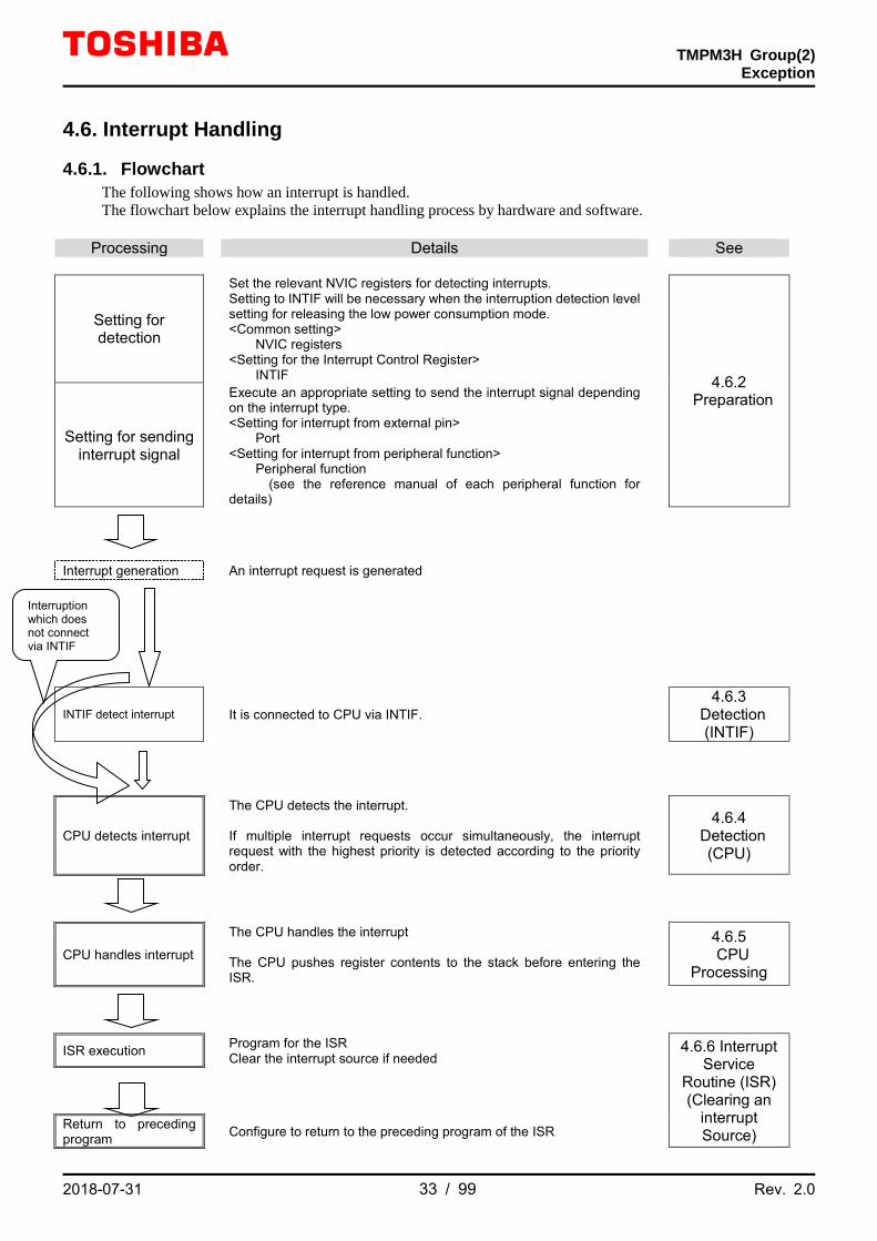
4.6. Interrupt Handling
4.6.1. Flowchart The following shows how an interrupt is handled. The flowchart below explains the interrupt handling process by hardware and software.
Processing Details See
Setting for detection
Set the relevant NVIC registers for detecting interrupts. Setting to INTIF will be necessary when the interruption detection level setting for releasing the low power consumption mode. <Common setting>
NVIC registers <Setting for the Interrupt Control Register>
INTIF
4.6.2 Preparation
Setting for sending interrupt signal
Execute an appropriate setting to send the interrupt signal depending on the interrupt type. <Setting for interrupt from external pin>
Port <Setting for interrupt from peripheral function>
Peripheral function (see the reference manual of each peripheral function for
details)
Interrupt generation An interrupt request is generated
INTIF detect interrupt
It is connected to CPU via INTIF. 4.6.3
Detection (INTIF)
CPU detects interrupt
The CPU detects the interrupt. If multiple interrupt requests occur simultaneously, the interrupt request with the highest priority is detected according to the priority order.
4.6.4
Detection (CPU)
CPU handles interrupt
The CPU handles the interrupt The CPU pushes register contents to the stack before entering the ISR.
4.6.5 CPU
Processing
ISR execution Program for the ISR
Clear the interrupt source if needed 4.6.6 Interrupt
Service Routine (ISR) (Clearing an
interrupt Source)
Return to preceding program
Configure to return to the preceding program of the ISR
Interruption which does not connect via INTIF
TMPM3H Group(2)
Exception
2018-07-31 34 / 99 Rev. 2.0
4.6.2. Preparation When preparing for an interrupt, you need to pay attention to the order of configuration to avoid any unexpected
interrupt on the way. Initiating an interrupt or changing its configuration must be implemented in the following order basically. First,
disable the interrupt by the CPU. Then, configure from the farthest route from the CPU. Finally, enable the interrupt by the CPU.
To configure the INTIF, you must follow the order indicated here not to cause any unexpected interrupt. First, configure the precondition. Secondly, clear the data related to the interrupt in the INTIF and then enable the interrupt.
The following sections are listed in the order of interrupt handling and describe how to configure them.
1. Disabling interrupt by CPU 2. CPU registers setting 3. Preconfiguration (1) (Interrupt from external pin) 4. Preconfiguration (2) (Interrupt from peripheral function) 5. Preconfiguration (3) (Interrupt Set-Pending Register) 6. Configuring the INTIF 7. Enabling interrupt by CPU
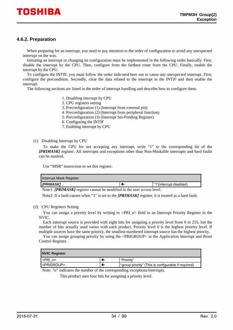
(1) Disabling Interrupt by CPU To make the CPU for not accepting any interrupt, write “1” to the corresponding bit of the
[PRIMASK] register. All interrupts and exceptions other than Non-Maskable interrupts and hard faults can be masked.
Use “MSR” instruction to set this register.
Interrupt Mask Register
[PRIMASK] “1”(interrupt disabled) Note1: [PRIMASK] register cannot be modified in the user access level. Note2: If a fault causes when “1” is set to the [PRIMASK] register, it is treated as a hard fault.
(2) CPU Registers Setting
You can assign a priority level by writing to <PRI_n> field in an Interrupt Priority Register in the NVIC.
Each interrupt source is provided with eight bits for assigning a priority level from 0 to 255, but the number of bits actually used varies with each product. Priority level 0 is the highest priority level. If multiple sources have the same priority, the smallest-numbered interrupt source has the highest priority.
You can assign grouping priority by using the <PRIGROUP> in the Application Interrupt and Reset Control Register.
NVIC Register
<PRI_n> “Priority” <PRIGROUP> “group priority” (This is configurable if required) Note: “n” indicates the number of the corresponding exceptions/interrupts.
This product uses four bits for assigning a priority level.
TMPM3H Group(2)
Exception
2018-07-31 35 / 99 Rev. 2.0
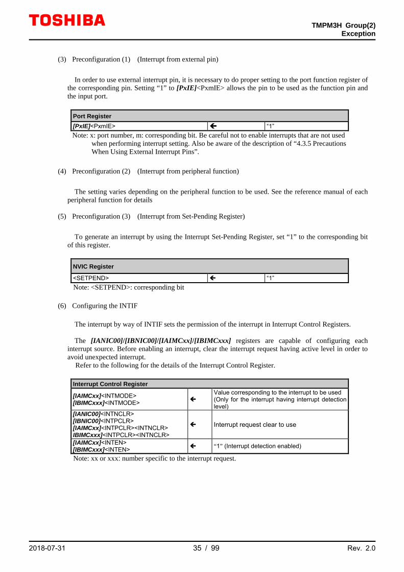
(3) Preconfiguration (1) (Interrupt from external pin)
In order to use external interrupt pin, it is necessary to do proper setting to the port function register of
the corresponding pin. Setting “1” to [PxIE]<PxmIE> allows the pin to be used as the function pin and the input port.
Port Register [PxIE]<PxmIE> “1” Note: x: port number, m: corresponding bit. Be careful not to enable interrupts that are not used
when performing interrupt setting. Also be aware of the description of “4.3.5 Precautions When Using External Interrupt Pins”.
(4) Preconfiguration (2) (Interrupt from peripheral function)
The setting varies depending on the peripheral function to be used. See the reference manual of each
peripheral function for details
(5) Preconfiguration (3) (Interrupt from Set-Pending Register) To generate an interrupt by using the Interrupt Set-Pending Register, set “1” to the corresponding bit
of this register.
NVIC Register
<SETPEND> “1” Note: <SETPEND>: corresponding bit
(6) Configuring the INTIF
The interrupt by way of INTIF sets the permission of the interrupt in Interrupt Control Registers. The [IANIC00]/[IBNIC00]/[IAIMCxx]/[IBIMCxxx] registers are capable of configuring each
interrupt source. Before enabling an interrupt, clear the interrupt request having active level in order to avoid unexpected interrupt.
Refer to the following for the details of the Interrupt Control Register.
Interrupt Control Register
[IAIMCxx]<INTMODE> [IBIMCxxx]<INTMODE>
Value corresponding to the interrupt to be used (Only for the interrupt having interrupt detection level)
[IANIC00]<INTNCLR> [IBNIC00]<INTPCLR> [IAIMCxx]<INTPCLR><INTNCLR> IBIMCxxx]<INTPCLR><INTNCLR>
Interrupt request clear to use
[IAIMCxx]<INTEN> [IBIMCxxx]<INTEN> “1” (Interrupt detection enabled)
Note: xx or xxx: number specific to the interrupt request.

TMPM3H Group(2)
Exception
2018-07-31 36 / 99 Rev. 2.0
(7) Enabling Interrupt by CPU
Enable the interrupt by the CPU as shown below. Clear the suspended interrupt in the Interrupt Clear-Pending Register. Enable the intended interrupt
with the Interrupt Set-Enable Register. Each bit of the register is assigned to a single interrupt source. Writing “1” to the corresponding bit of the Interrupt Clear-Pending Register clears the suspended
interrupt. Writing “1” to the corresponding bit of the Interrupt Set-Enable Register enables the intended interrupt.
To generate interrupts in the Interrupt Set-Pending Register setting, factors to trigger interrupts are lost if pending interrupts are cleared. Thus, this operation is not necessary.
At the end, [PRIMASK] register is zero cleared.
NVIC Register <CLRPEND> “1” <SETENA> “1”
Interrupt Mask Register [PRIMASK] “0”
Note1: <CLRPEND>,<SETENA>: corresponding bit Note2: [PRIMASK] Register cannot be modified by the user access level.
4.6.3. Detection (INTIF)
When the INTIF detects an interrupt request, it sends the interrupt signal in “High” level to the CPU. INTIF has the functions of the interruption detection level selection logic, the functions of detection logic, and the function of the interrupt enable/disable. Each function of INTIF is set up the Interrupt Control Register A or B. It keeps sending the interrupt signal in “High” level to the CPU until the Detection flag is cleared in the Interrupt Control Register. If the ISR is exited without clearing the Detection flag, the same interrupt will be detected again when normal operation is resumed. Thus, be sure to clear each Detection flag in the ISR. At the same time, the corresponding interrupt monitor register is also cleared.
4.6.4. Detection (CPU) The CPU detects an interrupt request with the highest priority.
4.6.5. CPU Processing On detecting an interrupt, the CPU pushes the contents of xPSR, PC, LR, r12, and r3-r0 to the stack then enter
the ISR.
TMPM3H Group(2)
Exception
2018-07-31 37 / 99 Rev. 2.0
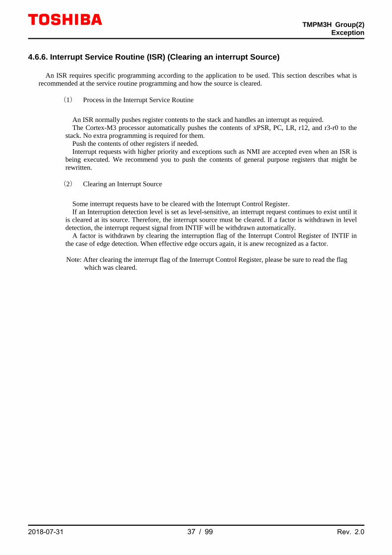
4.6.6. Interrupt Service Routine (ISR) (Clearing an interrupt Source) An ISR requires specific programming according to the application to be used. This section describes what is
recommended at the service routine programming and how the source is cleared.
(1) Process in the Interrupt Service Routine An ISR normally pushes register contents to the stack and handles an interrupt as required. The Cortex-M3 processor automatically pushes the contents of xPSR, PC, LR, r12, and r3-r0 to the
stack. No extra programming is required for them. Push the contents of other registers if needed. Interrupt requests with higher priority and exceptions such as NMI are accepted even when an ISR is
being executed. We recommend you to push the contents of general purpose registers that might be rewritten.
(2) Clearing an Interrupt Source
Some interrupt requests have to be cleared with the Interrupt Control Register. If an Interruption detection level is set as level-sensitive, an interrupt request continues to exist until it
is cleared at its source. Therefore, the interrupt source must be cleared. If a factor is withdrawn in level detection, the interrupt request signal from INTIF will be withdrawn automatically.
A factor is withdrawn by clearing the interruption flag of the Interrupt Control Register of INTIF in the case of edge detection. When effective edge occurs again, it is anew recognized as a factor.
Note: After clearing the interrupt flag of the Interrupt Control Register, please be sure to read the flag
which was cleared.
TMPM3H Group(2)
Exception
2018-07-31 38 / 99 Rev. 2.0
5. Exception/ Interrupt-Related Registers
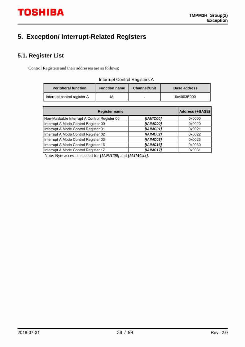
5.1. Register List Control Registers and their addresses are as follows;
Interrupt Control Registers A
Peripheral function Function name Channel/Unit Base address
Interrupt control register A IA - 0x4003E000
Register name Address (+BASE)
Non-Maskable Interrupt A Control Register 00 [IANIC00] 0x0000 Interrupt A Mode Control Register 00 [IAIMC00] 0x0020 Interrupt A Mode Control Register 01 [IAIMC01] 0x0021 Interrupt A Mode Control Register 02 [IAIMC02] 0x0022 Interrupt A Mode Control Register 03 [IAIMC03] 0x0023 Interrupt A Mode Control Register 16 [IAIMC16] 0x0030 Interrupt A Mode Control Register 17 [IAIMC17] 0x0031 Note: Byte access is needed for [IANIC00] and [IAIMCxx].

TMPM3H Group(2)
Exception
2018-07-31 39 / 99 Rev. 2.0
Interrupt Control Registers B
Peripheral function Function name Channel/Unit Base address
Interrupt control register B IB - 0x400F4E00
Register name Address (+BASE)
Non-Maskable Interrupt B Control Register 00 [IBNIC00] 0x0010
Interrupt B Mode Control Register 000 [IBIMC000] 0x0060
Interrupt B Mode Control Register 001 [IBIMC001] 0x0061
Interrupt B Mode Control Register 002 [IBIMC002] 0x0062
Interrupt B Mode Control Register 003 [IBIMC003] 0x0063
Interrupt B Mode Control Register 004 [IBIMC004] 0x0064
Interrupt B Mode Control Register 005 [IBIMC005] 0x0065
Interrupt B Mode Control Register 006 [IBIMC006] 0x0066
Interrupt B Mode Control Register 007 [IBIMC007] 0x0067
Interrupt B Mode Control Register 008 [IBIMC008] 0x0068
Interrupt B Mode Control Register 009 [IBIMC009] 0x0069
Interrupt B Mode Control Register 010 [IBIMC010] 0x006A
Interrupt B Mode Control Register 011 [IBIMC011] 0x006B
Interrupt B Mode Control Register 012 [IBIMC012] 0x006C
Interrupt B Mode Control Register 013 [IBIMC013] 0x006D
Interrupt B Mode Control Register 014 [IBIMC014] 0x006E
Interrupt B Mode Control Register 015 [IBIMC015] 0x006F
Interrupt B Mode Control Register 016 [IBIMC016] 0x0070
Interrupt B Mode Control Register 017 [IBIMC017] 0x0071
Interrupt B Mode Control Register 018 [IBIMC018] 0x0072
Interrupt B Mode Control Register 019 [IBIMC019] 0x0073
Interrupt B Mode Control Register 020 [IBIMC020] 0x0074
Interrupt B Mode Control Register 021 [IBIMC021] 0x0075
Interrupt B Mode Control Register 022 [IBIMC022] 0x0076
Interrupt B Mode Control Register 023 [IBIMC023] 0x0077
Interrupt B Mode Control Register 024 [IBIMC024] 0x0078
Interrupt B Mode Control Register 025 [IBIMC025] 0x0079
Interrupt B Mode Control Register 026 [IBIMC026] 0x007A
Interrupt B Mode Control Register 027 [IBIMC027] 0x007B
Interrupt B Mode Control Register 028 [IBIMC028] 0x007C
Interrupt B Mode Control Register 029 [IBIMC029] 0x007D
Interrupt B Mode Control Register 030 [IBIMC030] 0x007E
Interrupt B Mode Control Register 031 [IBIMC031] 0x007F
Interrupt B Mode Control Register 032 [IBIMC032] 0x0080
Interrupt B Mode Control Register 033 [IBIMC033] 0x0081
Interrupt B Mode Control Register 034 [IBIMC034] 0x0082
Interrupt B Mode Control Register 035 [IBIMC035] 0x0083
Interrupt B Mode Control Register 036 [IBIMC036] 0x0084
TMPM3H Group(2)
Exception
2018-07-31 40 / 99 Rev. 2.0
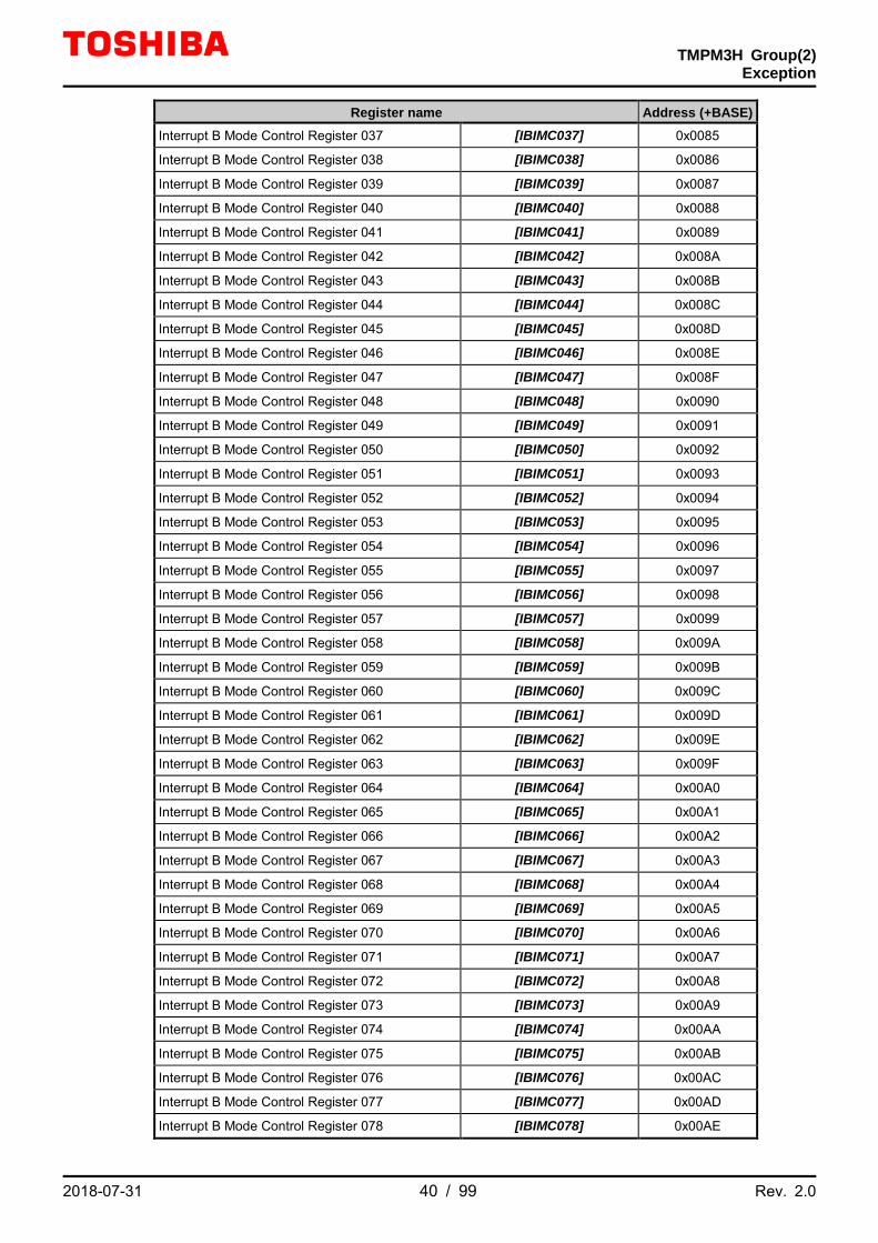
Register name Address (+BASE) Interrupt B Mode Control Register 037 [IBIMC037] 0x0085
Interrupt B Mode Control Register 038 [IBIMC038] 0x0086
Interrupt B Mode Control Register 039 [IBIMC039] 0x0087
Interrupt B Mode Control Register 040 [IBIMC040] 0x0088
Interrupt B Mode Control Register 041 [IBIMC041] 0x0089
Interrupt B Mode Control Register 042 [IBIMC042] 0x008A
Interrupt B Mode Control Register 043 [IBIMC043] 0x008B
Interrupt B Mode Control Register 044 [IBIMC044] 0x008C
Interrupt B Mode Control Register 045 [IBIMC045] 0x008D
Interrupt B Mode Control Register 046 [IBIMC046] 0x008E
Interrupt B Mode Control Register 047 [IBIMC047] 0x008F
Interrupt B Mode Control Register 048 [IBIMC048] 0x0090
Interrupt B Mode Control Register 049 [IBIMC049] 0x0091
Interrupt B Mode Control Register 050 [IBIMC050] 0x0092
Interrupt B Mode Control Register 051 [IBIMC051] 0x0093
Interrupt B Mode Control Register 052 [IBIMC052] 0x0094
Interrupt B Mode Control Register 053 [IBIMC053] 0x0095
Interrupt B Mode Control Register 054 [IBIMC054] 0x0096
Interrupt B Mode Control Register 055 [IBIMC055] 0x0097
Interrupt B Mode Control Register 056 [IBIMC056] 0x0098
Interrupt B Mode Control Register 057 [IBIMC057] 0x0099
Interrupt B Mode Control Register 058 [IBIMC058] 0x009A
Interrupt B Mode Control Register 059 [IBIMC059] 0x009B
Interrupt B Mode Control Register 060 [IBIMC060] 0x009C
Interrupt B Mode Control Register 061 [IBIMC061] 0x009D
Interrupt B Mode Control Register 062 [IBIMC062] 0x009E
Interrupt B Mode Control Register 063 [IBIMC063] 0x009F
Interrupt B Mode Control Register 064 [IBIMC064] 0x00A0
Interrupt B Mode Control Register 065 [IBIMC065] 0x00A1
Interrupt B Mode Control Register 066 [IBIMC066] 0x00A2
Interrupt B Mode Control Register 067 [IBIMC067] 0x00A3
Interrupt B Mode Control Register 068 [IBIMC068] 0x00A4
Interrupt B Mode Control Register 069 [IBIMC069] 0x00A5
Interrupt B Mode Control Register 070 [IBIMC070] 0x00A6
Interrupt B Mode Control Register 071 [IBIMC071] 0x00A7
Interrupt B Mode Control Register 072 [IBIMC072] 0x00A8
Interrupt B Mode Control Register 073 [IBIMC073] 0x00A9
Interrupt B Mode Control Register 074 [IBIMC074] 0x00AA
Interrupt B Mode Control Register 075 [IBIMC075] 0x00AB
Interrupt B Mode Control Register 076 [IBIMC076] 0x00AC
Interrupt B Mode Control Register 077 [IBIMC077] 0x00AD
Interrupt B Mode Control Register 078 [IBIMC078] 0x00AE
TMPM3H Group(2)
Exception
2018-07-31 41 / 99 Rev. 2.0
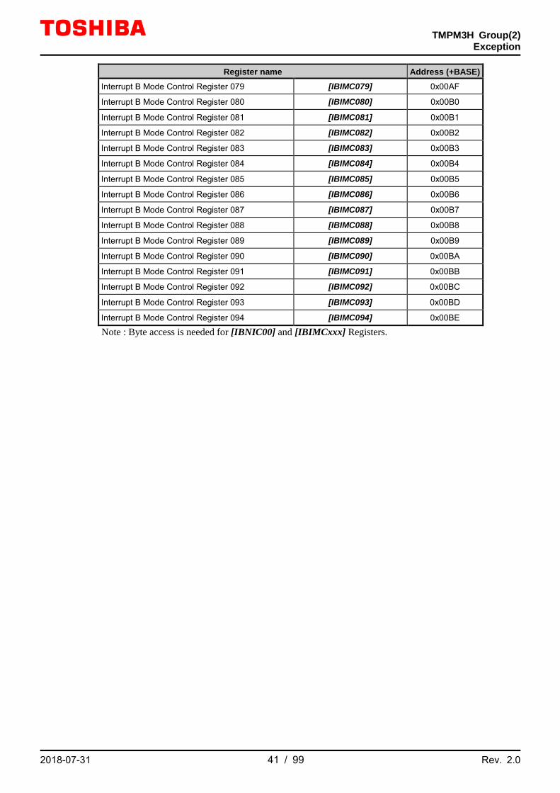
Register name Address (+BASE) Interrupt B Mode Control Register 079 [IBIMC079] 0x00AF
Interrupt B Mode Control Register 080 [IBIMC080] 0x00B0
Interrupt B Mode Control Register 081 [IBIMC081] 0x00B1
Interrupt B Mode Control Register 082 [IBIMC082] 0x00B2
Interrupt B Mode Control Register 083 [IBIMC083] 0x00B3
Interrupt B Mode Control Register 084 [IBIMC084] 0x00B4
Interrupt B Mode Control Register 085 [IBIMC085] 0x00B5
Interrupt B Mode Control Register 086 [IBIMC086] 0x00B6
Interrupt B Mode Control Register 087 [IBIMC087] 0x00B7
Interrupt B Mode Control Register 088 [IBIMC088] 0x00B8
Interrupt B Mode Control Register 089 [IBIMC089] 0x00B9
Interrupt B Mode Control Register 090 [IBIMC090] 0x00BA
Interrupt B Mode Control Register 091 [IBIMC091] 0x00BB
Interrupt B Mode Control Register 092 [IBIMC092] 0x00BC
Interrupt B Mode Control Register 093 [IBIMC093] 0x00BD
Interrupt B Mode Control Register 094 [IBIMC094] 0x00BE
Note : Byte access is needed for [IBNIC00] and [IBIMCxxx] Registers.

TMPM3H Group(2)
Exception
2018-07-31 42 / 99 Rev. 2.0
Reset Flag Registers
Peripheral function Function name Channel/Unit Base address
Low speed oscillation/power control/reset RLM - 0x4003E400
Register name Address (+BASE)
Reset Flag Register 0 [RLMRSTFLG0] 0x0002 Reset Flag Register 1 [RLMRSTFLG1] 0x0003
Note: Byte access is needed for Reset Flag Register.
Interrupt Monitor Registers
Peripheral function Function name Channel/Unit Base address
Interrupt Monitor IMN - 0x400F4F00
Register name Address (+BASE))
Non-Maskable Interrupt Monitor Flag Register [IMNFLGNMI] 0x0000 Interrupt Monitor Flag Register 1 [IMNFLG1] 0x0004 Interrupt Monitor Flag Register 3 [IMNFLG3] 0x000C Interrupt Monitor Flag Register 4 [IMNFLG4] 0x0010 Interrupt Monitor Flag Register 5 [IMNFLG5] 0x0014

TMPM3H Group(2)
Exception
2018-07-31 43 / 99 Rev. 2.0
NVIC Registers
Peripheral function Channel/Unit Base address
NVIC Register - 0xE000E000
Register name Address(Base +)
SysTick Control and Status Register 0x0010 SysTick Reload Value Register 0x0014 SysTick Current Value Register 0x0018 SysTick Calibration Value Register 0x001C Interrupt Set-Enable Register0 0x0100 Interrupt Set-Enable Register1 0x0104 Interrupt Set-Enable Register2 0x0108 Interrupt Set-Enable Register3 0x010C Interrupt Set-Enable Register4 0x0110 Interrupt Set-Enable Register5 0x0114 Interrupt Clear-Enable Register0 0x0180 Interrupt Clear-Enable Register1 0x0184 Interrupt Clear-Enable Register2 0x0188 Interrupt Clear-Enable Register3 0x018C Interrupt Clear-Enable Register4 0x0190 Interrupt Clear-Enable Register5 0x0194 Interrupt Set-Pending Register0 0x0200 Interrupt Set-Pending Register1 0x0204 Interrupt Set-Pending Register2 0x0208 Interrupt Set-Pending Register3 0x020C Interrupt Set-Pending Register4 0x0210 Interrupt Set-Pending Register5 0x0214 Interrupt Clear-Pending Register0 0x0280 Interrupt Clear-Pending Register1 0x0284 Interrupt Clear-Pending Register2 0x0288 Interrupt Clear-Pending Register3 0x028C Interrupt Clear-Pending Register4 0x0290 Interrupt Clear-Pending Register5 0x0294 Interrupt Priority Register 0x0400 to 0x04A5 Vector Table Offset Register 0x0D08 Application Interrupt and Reset Control Register 0x0D0C System Handler Priority Register 0x0D18, 0x0D1C, 0x0D20 System Handler Control and State Register 0x0D24

TMPM3H Group(2)
Exception
2018-07-31 44 / 99 Rev. 2.0
5.2. Interrupt Control Registers A
5.2.1. [IANIC00] (Non-Maskable Interrupt A Control Register 00)
Bit Bit Symbol After reset Type Function
7 INTNCLR 0 W
Detection flag clear control 0: - 1: Clear Read as “0”
6 - 0 R Read as “0”
5 INTNFLG 0 R Detection flag 0: Not detected 1: Detected
4:0 - 00101 R Read as “00101”
5.2.2. [IAIMC00 to 03,16 to 17] (Interrupt A Mode Control Register n) (1) [IAIMC00 to 03] Registers
Bit Bit Symbol After Reset Type Function
7 INTNCLR 0 W
Falling edge detection flag clear control 0: - 1: Clear Read as “0”
6 INTPCLR 0 W
Rising edge detection flag clear control 0: - 1: Clear Read as “0”
5 INTNFLG 0 R Falling edge detection flag 0: Not detected 1: Detected
4 INTPFLG 0 R Rising edge detection flag 0: Not detected 1: Detected
3:1 INTMODE[2:0] 000 R/W
Interruption detection level selection 000: Low level 001: High level 010: Falling edge 011: Rising edge 100: Both edge 101: Reserved 110: Reserved 111: Reserved
0 INTEN 0 R/W Interrupt control 0: Interrupt detection disabled 1: Interrupt detection enabled

TMPM3H Group(2)
Exception
2018-07-31 45 / 99 Rev. 2.0
(2) [IAIMC16] Register
Bit Bit Symbol After Reset Type Function
7 - 0 R Read as “0”
6 INTPCLR 0 W
Detection flag clear control 0: - 1: Clear Read as “0”
5 - 0 R Read as “0”
4 INTPFLG 0 R Detection flag 0: Not detected 1: Detected
3:1 - 011 R Read as “011”
0 INTEN 0 R/W Interrupt control 0: Interrupt detection disabled 1: Interrupt detection enabled
(3) [IAIMC17] Register
Bit Bit Symbol After Reset Type Function
7 INTNCLR 0 W
Detection flag clear control 0: - 1: Clear Read as “0”
6 - 0 R Read as “0”
5 INTNFLG 0 R Detection flag 0: Not detected 1: Detected
4:1 - 0010 R Read as “0010”
0 INTEN 0 R/W Interrupt control 0: Interrupt detection disabled 1: Interrupt detection enabled

TMPM3H Group(2)
Exception
2018-07-31 46 / 99 Rev. 2.0
5.3. Interrupt Control Registers B
5.3.1. [IBNIC00] (Non-Maskable Interrupt B Control Register 00)
Bit Bit Symbol After Reset Type Function
7 - 0 R Read as “0”
6 INTPCLR 0 W
Detection flag clear control 0: - 1: Clear Read as “0”
5 - 0 R Read as “0”
4 INTPFLG 0 R Detection flag 0: Not detected 1: Detected
3:0 - 0111 R Read as “0111”
5.3.2. [IBIMC000 to 065, 066 to 093, 094] (Interrupt B Mode Control Register n) (1) [IBIMC000 to 065] Registers
Bit Bit Symbol After Reset Type Function
7 - 0 R Read as “0”
6 INTPCLR 0 W
Detection flag clear control 0: - 1: Clear Read as “0”
5 - 0 R Read as “0”
4 INTPFLG 0 R Detection flag 0: Not detected 1: Detected
3:0 - 0111 R Read as”0111”
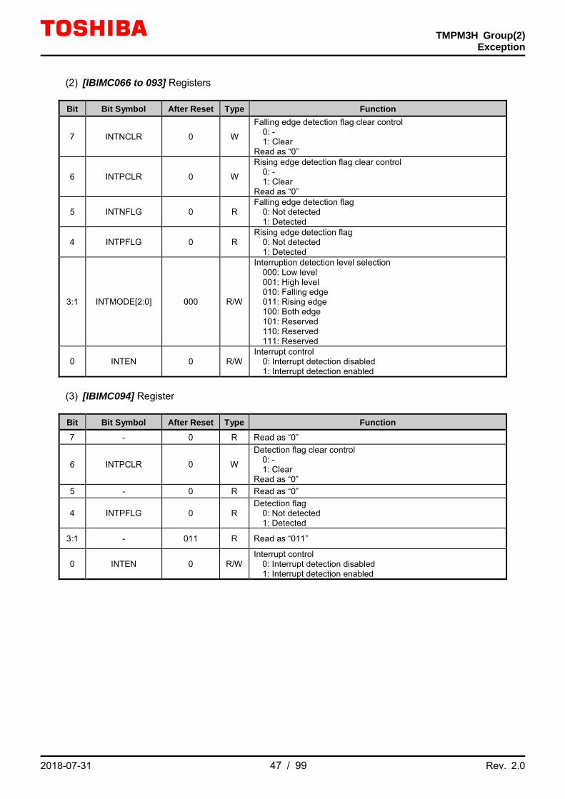
TMPM3H Group(2)
Exception
2018-07-31 47 / 99 Rev. 2.0
(2) [IBIMC066 to 093] Registers
Bit Bit Symbol After Reset Type Function
7 INTNCLR 0 W
Falling edge detection flag clear control 0: - 1: Clear Read as “0”
6 INTPCLR 0 W
Rising edge detection flag clear control 0: - 1: Clear Read as “0”
5 INTNFLG 0 R Falling edge detection flag 0: Not detected 1: Detected
4 INTPFLG 0 R Rising edge detection flag 0: Not detected 1: Detected
3:1 INTMODE[2:0] 000 R/W
Interruption detection level selection 000: Low level 001: High level 010: Falling edge 011: Rising edge 100: Both edge 101: Reserved 110: Reserved 111: Reserved
0 INTEN 0 R/W Interrupt control 0: Interrupt detection disabled 1: Interrupt detection enabled
(3) [IBIMC094] Register
Bit Bit Symbol After Reset Type Function
7 - 0 R Read as “0”
6 INTPCLR 0 W
Detection flag clear control 0: - 1: Clear Read as “0”
5 - 0 R Read as “0”
4 INTPFLG 0 R Detection flag 0: Not detected 1: Detected
3:1 - 011 R Read as “011”
0 INTEN 0 R/W Interrupt control 0: Interrupt detection disabled 1: Interrupt detection enabled
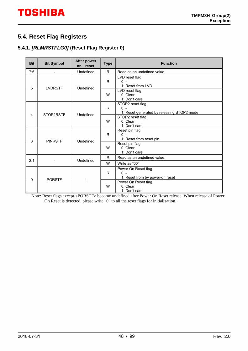
TMPM3H Group(2)
Exception
2018-07-31 48 / 99 Rev. 2.0
5.4. Reset Flag Registers
5.4.1. [RLMRSTFLG0] (Reset Flag Register 0)
Bit Bit Symbol After power on reset Type Function
7:6 - Undefined R Read as an undefined value.
5 LVDRSTF Undefined
R LVD reset flag 0: - 1: Reset from LVD
W LVD reset flag 0: Clear 1: Don’t care
4 STOP2RSTF Undefined
R STOP2 reset flag 0: - 1: Reset generated by releasing STOP2 mode
W STOP2 reset flag 0: Clear 1: Don’t care
3 PINRSTF Undefined
R Reset pin flag 0: - 1: Reset from reset pin
W Reset pin flag 0: Clear 1: Don’t care
2:1 - Undefined R Read as an undefined value. W Write as “00”
0 PORSTF 1
R Power On Reset flag 0: - 1: Reset from by power-on reset
W Power On Reset flag 0: Clear 1: Don’t care
Note: Reset flags except <PORSTF> become undefined after Power On Reset release. When release of Power On Reset is detected, please write "0" to all the reset flags for initialization.
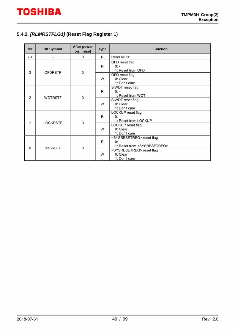
TMPM3H Group(2)
Exception
2018-07-31 49 / 99 Rev. 2.0
5.4.2. [RLMRSTFLG1] (Reset Flag Register 1)
Bit Bit Symbol After power on reset Type Function
7:4 - 0 R Read as “0”
3 OFDRSTF 0
R OFD reset flag 0: - 1: Reset from OFD
W OFD reset flag 0: Clear 1: Don’t care
2 WDTRSTF 0
R SIWDT reset flag 0: - 1: Reset from WDT
W SIWDT reset flag 0: Clear 1: Don’t care
1 LOCKRSTF 0
R LOCKUP reset flag 0: - 1: Reset from LOCKUP
W LOCKUP reset flag 0: Clear 1: Don’t care
0 SYSRSTF 0
R <SYSRESETREQ> reset flag 0: - 1: Reset from <SYSRESETREQ>
W <SYSRESETREQ> reset flag 0: Clear 1: Don’t care
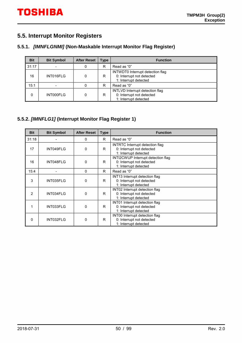
TMPM3H Group(2)
Exception
2018-07-31 50 / 99 Rev. 2.0
5.5. Interrupt Monitor Registers
5.5.1. [IMNFLGNMI] (Non-Maskable Interrupt Monitor Flag Register)
Bit Bit Symbol After Reset Type Function
31:17 - 0 R Read as “0”
16 INT016FLG 0 R INTWDT0 Interrupt detection flag 0: Interrupt not detected 1: Interrupt detected
15:1 - 0 R Read as “0”
0 INT000FLG 0 R INTLVD Interrupt detection flag 0: Interrupt not detected 1: Interrupt detected
5.5.2. [IMNFLG1] (Interrupt Monitor Flag Register 1)
Bit Bit Symbol After Reset Type Function
31:18 - 0 R Read as “0”
17 INT049FLG 0 R INTRTC Interrupt detection flag 0: Interrupt not detected 1: Interrupt detected
16 INT048FLG 0 R INTI2CWUP Interrupt detection flag 0: Interrupt not detected 1: Interrupt detected
15:4 - 0 R Read as “0”
3 INT035FLG 0 R INT13 Interrupt detection flag 0: Interrupt not detected 1: Interrupt detected
2 INT034FLG 0 R INT02 Interrupt detection flag 0: Interrupt not detected 1: Interrupt detected
1 INT033FLG 0 R INT01 Interrupt detection flag 0: Interrupt not detected 1: Interrupt detected
0 INT032FLG 0 R INT00 Interrupt detection flag 0: Interrupt not detected 1: Interrupt detected

TMPM3H Group(2)
Exception
2018-07-31 51 / 99 Rev. 2.0
5.5.3. [IMNFLG3] (Interrupt Monitor Flag Register 3)
Bit Bit Symbol After Reset Type Function
31 INT127FLG 0 R INTDMAATC(ch31) Interrupt detection flag 0: Interrupt not detected 1: Interrupt detected
30 INT126FLG 0 R INTDMAATC(ch30) Interrupt detection flag 0: Interrupt not detected 1: Interrupt detected
29 INT125FLG 0 R INTDMAATC(ch29) Interrupt detection flag 0: Interrupt not detected 1: Interrupt detected
28 INT124FLG 0 R INTDMAATC(ch28) Interrupt detection flag 0: Interrupt not detected 1: Interrupt detected
27 INT123FLG 0 R INTDMAATC(ch27) Interrupt detection flag 0: Interrupt not detected 1: Interrupt detected
26 INT122FLG 0 R INTDMAATC(ch26) Interrupt detection flag 0: Interrupt not detected 1: Interrupt detected
25 INT121FLG 0 R INTDMAATC(ch25) Interrupt detection flag 0: Interrupt not detected 1: Interrupt detected
24 INT120FLG 0 R INTDMAATC(ch24) Interrupt detection flag 0: Interrupt not detected 1: Interrupt detected
23 INT119FLG 0 R INTDMAATC(ch23) Interrupt detection flag 0: Interrupt not detected 1: Interrupt detected
22 INT118FLG 0 R INTDMAATC(ch22) Interrupt detection flag 0: Interrupt not detected 1: Interrupt detected
21 INT117FLG 0 R INTDMAATC(ch21) Interrupt detection flag 0: Interrupt not detected 1: Interrupt detected
20 INT116FLG 0 R INTDMAATC(ch20) Interrupt detection flag 0: Interrupt not detected 1: Interrupt detected
19 INT115FLG 0 R INTDMAATC(ch19) Interrupt detection flag 0: Interrupt not detected 1: Interrupt detected
18 INT114FLG 0 R INTDMAATC(ch18) Interrupt detection flag 0: Interrupt not detected 1: Interrupt detected
17 INT113FLG 0 R INTDMAATC(ch17) Interrupt detection flag 0: Interrupt not detected 1: Interrupt detected
16 INT112FLG 0 R INTDMAATC(ch16) Interrupt detection flag 0: Interrupt not detected 1: Interrupt detected
15 INT111FLG 0 R INTDMAATC(ch15) Interrupt detection flag 0: Interrupt not detected 1: Interrupt detected
14 INT110FLG 0 R INTDMAATC(ch14) Interrupt detection flag 0: Interrupt not detected 1: Interrupt detected
13 INT109FLG 0 R INTDMAATC(ch13) Interrupt detection flag 0: Interrupt not detected 1: Interrupt detected
12 INT108FLG 0 R INTDMAATC(ch12) Interrupt detection flag 0: Interrupt not detected 1: Interrupt detected
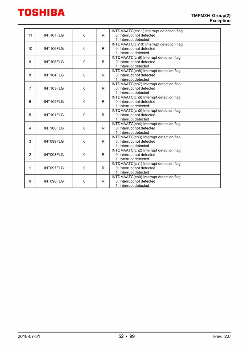
TMPM3H Group(2)
Exception
2018-07-31 52 / 99 Rev. 2.0
11 INT107FLG 0 R INTDMAATC(ch11) Interrupt detection flag 0: Interrupt not detected 1: Interrupt detected
10 INT106FLG 0 R INTDMAATC(ch10) Interrupt detection flag 0: Interrupt not detected 1: Interrupt detected
9 INT105FLG 0 R INTDMAATC(ch9) Interrupt detection flag 0: Interrupt not detected 1: Interrupt detected
8 INT104FLG 0 R INTDMAATC(ch8) Interrupt detection flag 0: Interrupt not detected 1: Interrupt detected
7 INT103FLG 0 R INTDMAATC(ch7) Interrupt detection flag 0: Interrupt not detected 1: Interrupt detected
6 INT102FLG 0 R INTDMAATC(ch6) Interrupt detection flag 0: Interrupt not detected 1: Interrupt detected
5 INT101FLG 0 R INTDMAATC(ch5) Interrupt detection flag 0: Interrupt not detected 1: Interrupt detected
4 INT100FLG 0 R INTDMAATC(ch4) Interrupt detection flag 0: Interrupt not detected 1: Interrupt detected
3 INT099FLG 0 R INTDMAATC(ch3) Interrupt detection flag 0: Interrupt not detected 1: Interrupt detected
2 INT098FLG 0 R INTDMAATC(ch2) Interrupt detection flag 0: Interrupt not detected 1: Interrupt detected
1 INT097FLG 0 R INTDMAATC(ch1) Interrupt detection flag 0: Interrupt not detected 1: Interrupt detected
0 INT096FLG 0 R INTDMAATC(ch0) Interrupt detection flag 0: Interrupt not detected 1: Interrupt detected

TMPM3H Group(2)
Exception
2018-07-31 53 / 99 Rev. 2.0
5.5.4. [IMNFLG4] (Interrupt Monitor Flag Register 4)
Bit Bit Symbol After Reset Type Function
31 INT159FLG 0 R INTDMABTC(ch30) Interrupt detection flag 0: Interrupt not detected 1: Interrupt detected
30 INT158FLG 0 R INTDMABTC(ch29) Interrupt detection flag 0: Interrupt not detected 1: Interrupt detected
29 INT157FLG 0 R INTDMABTC(ch28) Interrupt detection flag 0: Interrupt not detected 1: Interrupt detected
28 INT156FLG 0 R INTDMABTC(ch27) Interrupt detection flag 0: Interrupt not detected 1: Interrupt detected
27 INT155FLG 0 R INTDMABTC(ch26) Interrupt detection flag 0: Interrupt not detected 1: Interrupt detected
26 INT154FLG 0 R INTDMABTC(ch25) Interrupt detection flag 0: Interrupt not detected 1: Interrupt detected
25 INT153FLG 0 R INTDMABTC(ch24) Interrupt detection flag 0: Interrupt not detected 1: Interrupt detected
24 INT152FLG 0 R INTDMABTC(ch23) Interrupt detection flag 0: Interrupt not detected 1: Interrupt detected
23 INT151FLG 0 R INTDMABTC(ch22) Interrupt detection flag 0: Interrupt not detected 1: Interrupt detected
22 INT150FLG 0 R INTDMABTC(ch21) Interrupt detection flag 0: Interrupt not detected 1: Interrupt detected
21 INT149FLG 0 R INTDMABTC(ch20) Interrupt detection flag 0: Interrupt not detected 1: Interrupt detected
20 INT148FLG 0 R INTDMABTC(ch19) Interrupt detection flag 0: Interrupt not detected 1: Interrupt detected
19 INT147FLG 0 R INTDMABTC(ch18) Interrupt detection flag 0: Interrupt not detected 1: Interrupt detected
18 INT146FLG 0 R INTDMABTC(ch17) Interrupt detection flag 0: Interrupt not detected 1: Interrupt detected
17 INT145FLG 0 R INTDMABTC(ch16) Interrupt detection flag 0: Interrupt not detected 1: Interrupt detected
16 INT144FLG 0 R INTDMABTC(ch15) Interrupt detection flag 0: Interrupt not detected 1: Interrupt detected
15 INT143FLG 0 R INTDMABTC(ch14) Interrupt detection flag 0: Interrupt not detected 1: Interrupt detected
14 INT142FLG 0 R INTDMABTC(ch13) Interrupt detection flag 0: Interrupt not detected 1: Interrupt detected
13 INT141FLG 0 R INTDMABTC(ch12) Interrupt detection flag 0: Interrupt not detected 1: Interrupt detected
12 INT140FLG 0 R INTDMABTC(ch11) Interrupt detection flag 0: Interrupt not detected 1: Interrupt detected

TMPM3H Group(2)
Exception
2018-07-31 54 / 99 Rev. 2.0
11 INT139FLG 0 R INTDMABTC(ch10) Interrupt detection flag 0: Interrupt not detected 1: Interrupt detected
10 INT138FLG 0 R INTDMABTC(ch9) Interrupt detection flag 0: Interrupt not detected 1: Interrupt detected
9 INT137FLG 0 R INTDMABTC(ch8) Interrupt detection flag 0: Interrupt not detected 1: Interrupt detected
8 INT136FLG 0 R INTDMABTC(ch7) Interrupt detection flag 0: Interrupt not detected 1: Interrupt detected
7 INT135FLG 0 R INTDMABTC(ch6) Interrupt detection flag 0: Interrupt not detected 1: Interrupt detected
6 INT134FLG 0 R INTDMABTC(ch5) Interrupt detection flag 0: Interrupt not detected 1: Interrupt detected
5 INT133FLG 0 R INTDMABTC(ch4) Interrupt detection flag 0: Interrupt not detected 1: Interrupt detected
4 INT132FLG 0 R INTDMABTC(ch3) Interrupt detection flag 0: Interrupt not detected 1: Interrupt detected
3 INT131FLG 0 R INTDMABTC(ch2) Interrupt detection flag 0: Interrupt not detected 1: Interrupt detected
2 INT130FLG 0 R INTDMABTC(ch1) Interrupt detection flag 0: Interrupt not detected 1: Interrupt detected
1 INT129FLG 0 R INTDMABTC(ch0) Interrupt detection flag 0: Interrupt not detected 1: Interrupt detected
0 INT128FLG 0 R INTDMAAERR Interrupt detection flag 0: Interrupt not detected 1: Interrupt detected

TMPM3H Group(2)
Exception
2018-07-31 55 / 99 Rev. 2.0
5.5.5. [IMNFLG5] (Interrupt Monitor Flag Register 5)
Bit Bit Symbol After Reset Type Function
31 - 0 R Read as “0”
30 INT190FLG 0 R INTRMC0 Interrupt detection flag 0: Interrupt not detected 1: Interrupt detected
29 INT189FLG 0 R INT31 Interrupt detection flag 0: Interrupt not detected 1: Interrupt detected
28 INT188FLG 0 R INT30 Interrupt detection flag 0: Interrupt not detected 1: Interrupt detected
27 INT187FLG 0 R INT29 Interrupt detection flag 0: Interrupt not detected 1: Interrupt detected
26 INT186FLG 0 R INT28 Interrupt detection flag 0: Interrupt not detected 1: Interrupt detected
25 INT185FLG 0 R INT27 Interrupt detection flag 0: Interrupt not detected 1: Interrupt detected
24 INT184FLG 0 R INT26 Interrupt detection flag 0: Interrupt not detected 1: Interrupt detected
23 INT183FLG 0 R INT25 Interrupt detection flag 0: Interrupt not detected 1: Interrupt detected
22 INT182FLG 0 R INT24 Interrupt detection flag 0: Interrupt not detected 1: Interrupt detected
21 INT181FLG 0 R INT23 Interrupt detection flag 0: Interrupt not detected 1: Interrupt detected
20 INT180FLG 0 R INT22 Interrupt detection flag 0: Interrupt not detected 1: Interrupt detected
19 INT179FLG 0 R INT21 Interrupt detection flag 0: Interrupt not detected 1: Interrupt detected
18 INT178FLG 0 R INT20 Interrupt detection flag 0: Interrupt not detected 1: Interrupt detected
17 INT177FLG 0 R INT19 Interrupt detection flag 0: Interrupt not detected 1: Interrupt detected
16 INT176FLG 0 R INT18 Interrupt detection flag 0: Interrupt not detected 1: Interrupt detected
15 INT175FLG 0 R INT17 Interrupt detection flag 0: Interrupt not detected 1: Interrupt detected
14 INT174FLG 0 R INT16 Interrupt detection flag 0: Interrupt not detected 1: Interrupt detected
13 INT173FLG 0 R INT15 Interrupt detection flag 0: Interrupt not detected 1: Interrupt detected
12 INT172FLG 0 R INT14 Interrupt detection flag 0: Interrupt not detected 1: Interrupt detected
11 INT171FLG 0 R INT12 Interrupt detection flag 0: Interrupt not detected 1: Interrupt detected
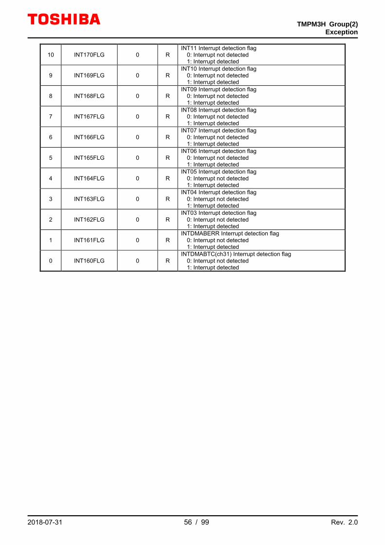
TMPM3H Group(2)
Exception
2018-07-31 56 / 99 Rev. 2.0
10 INT170FLG 0 R INT11 Interrupt detection flag 0: Interrupt not detected 1: Interrupt detected
9 INT169FLG 0 R INT10 Interrupt detection flag 0: Interrupt not detected 1: Interrupt detected
8 INT168FLG 0 R INT09 Interrupt detection flag 0: Interrupt not detected 1: Interrupt detected
7 INT167FLG 0 R INT08 Interrupt detection flag 0: Interrupt not detected 1: Interrupt detected
6 INT166FLG 0 R INT07 Interrupt detection flag 0: Interrupt not detected 1: Interrupt detected
5 INT165FLG 0 R INT06 Interrupt detection flag 0: Interrupt not detected 1: Interrupt detected
4 INT164FLG 0 R INT05 Interrupt detection flag 0: Interrupt not detected 1: Interrupt detected
3 INT163FLG 0 R INT04 Interrupt detection flag 0: Interrupt not detected 1: Interrupt detected
2 INT162FLG 0 R INT03 Interrupt detection flag 0: Interrupt not detected 1: Interrupt detected
1 INT161FLG 0 R INTDMABERR Interrupt detection flag 0: Interrupt not detected 1: Interrupt detected
0 INT160FLG 0 R INTDMABTC(ch31) Interrupt detection flag 0: Interrupt not detected 1: Interrupt detected
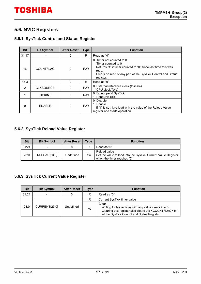
TMPM3H Group(2)
Exception
2018-07-31 57 / 99 Rev. 2.0
5.6. NVIC Registers
5.6.1. SysTick Control and Status Register
5.6.2. SysTick Reload Value Register
5.6.3. SysTick Current Value Register
Bit Bit Symbol After Reset Type Function
31:17 - 0 R Read as “0”
16 COUNTFLAG 0 R/W
0: Timer not counted to 0 1: Timer counted to 0 Returns “1” if timer counted to “0” since last time this was
read. Clears on read of any part of the SysTick Control and Status register.
15:3 - 0 R Read as “0”
2 CLKSOURCE 0 R/W 0: External reference clock (fosc/64) 1: CPU clock(fsys)
1 TICKINT 0 R/W 0: Do not pend SysTick 1: Pend SysTick
0 ENABLE 0 R/W
0: Disable 1: Enable If “1” is set, it re-load with the value of the Reload Value register and starts operation.
Bit Bit Symbol After Reset Type Function
31:24 - 0 R Read as “0”
23:0 RELOAD[23:0] Undefined R/W Reload value Set the value to load into the SysTick Current Value Register when the timer reaches “0”.
Bit Bit Symbol After Reset Type Function
31:24 - 0 R Read as “0”
23:0 CURRENT[23:0] Undefined
R Current SysTick timer value
W
Clear Writing to this register with any value clears it to 0. Clearing this register also clears the <COUNTFLAG> bit
of the SysTick Control and Status Register.

TMPM3H Group(2)
Exception
2018-07-31 58 / 99 Rev. 2.0
5.6.4. SysTick Calibration Value Register
Note: This product does not prepare the calibration value.
Bit Bit Symbol After Reset Type Function
31 NOREF 0 R 0: Reference clock provided 1: No reference clock
30 SKEW 1 R 0: Calibration value is 10ms. 1: Calibration value is not 10ms.
29:24 - 0 R Read as “0”
23:0 TENMS 0x000000 R Calibration value (Note)
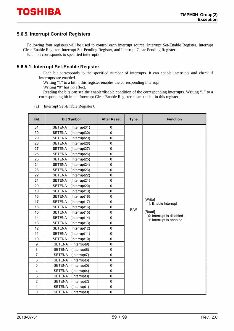
TMPM3H Group(2)
Exception
2018-07-31 59 / 99 Rev. 2.0
5.6.5. Interrupt Control Registers Following four registers will be used to control each interrupt source; Interrupt Set-Enable Register, Interrupt
Clear-Enable Register, Interrupt Set-Pending Register, and Interrupt Clear-Pending Register. Each bit corresponds to specified interruption.
5.6.5.1. Interrupt Set-Enable Register Each bit corresponds to the specified number of interrupts. It can enable interrupts and check if
interrupts are enabled. Writing “1” to a bit in this register enables the corresponding interrupt. Writing “0” has no effect. Reading the bits can see the enable/disable condition of the corresponding interrupts. Writing “1” to a
corresponding bit in the Interrupt Clear-Enable Register clears the bit in this register.
(a) Interrupt Set-Enable Register 0
Bit Bit Symbol After Reset Type Function
31 SETENA (Interrupt31) 0
R/W
[Write] 1: Enable interrupt [Read] 0: Interrupt is disabled 1: Interrupt is enabled
30 SETENA (Interrupt30) 0 29 SETENA (Interrupt29) 0 28 SETENA (Interrupt28) 0 27 SETENA (Interrupt27) 0 26 SETENA (Interrupt26) 0 25 SETENA (Interrupt25) 0 24 SETENA (Interrupt24) 0 23 SETENA (Interrupt23) 0 22 SETENA (Interrupt22) 0 21 SETENA (Interrupt21) 0 20 SETENA (Interrupt20) 0 19 SETENA (Interrupt19) 0 18 SETENA (Interrupt18) 0 17 SETENA (Interrupt17) 0 16 SETENA (Interrupt16) 0 15 SETENA (Interrupt15) 0 14 SETENA (Interrupt14) 0 13 SETENA (Interrupt13) 0 12 SETENA (Interrupt12) 0 11 SETENA (Interrupt11) 0 10 SETENA (Interrupt10) 0 9 SETENA (Interrupt9) 0 8 SETENA (Interrupt8) 0 7 SETENA (Interrupt7) 0 6 SETENA (Interrupt6) 0 5 SETENA (Interrupt5) 0 4 SETENA (Interrupt4) 0 3 SETENA (Interrupt3) 0 2 SETENA (Interrupt2) 0 1 SETENA (Interrupt1) 0 0 SETENA (Interrupt0) 0

TMPM3H Group(2)
Exception
2018-07-31 60 / 99 Rev. 2.0
(b) Interrupt Set-Enable Register 1
Bit Bit Symbol After Reset Type Function
31 SETENA (Interrupt63) 0
R/W
[Write] 1: Enable interrupt [Read] 0: Interrupt is disabled 1: Interrupt is enabled
30 SETENA (Interrupt62) 0 29 SETENA (Interrupt61) 0 28 SETENA (Interrupt60) 0 27 SETENA (Interrupt59) 0 26 SETENA (Interrupt58) 0 25 SETENA (Interrupt57) 0 24 SETENA (Interrupt56) 0 23 SETENA (Interrupt55) 0 22 SETENA (Interrupt54) 0 21 SETENA (Interrupt53) 0 20 SETENA (Interrupt52) 0 19 SETENA (Interrupt51) 0 18 SETENA (Interrupt50) 0 17 SETENA (Interrupt49) 0 16 SETENA (Interrupt48) 0 15 SETENA (Interrupt47) 0 14 SETENA (Interrupt46) 0 13 SETENA (Interrupt45) 0 12 SETENA (Interrupt44) 0 11 SETENA (Interrupt43) 0 10 SETENA (Interrupt42) 0 9 SETENA (Interrupt41) 0 8 SETENA (Interrupt40) 0 7 SETENA (Interrupt39) 0 6 SETENA (Interrupt38) 0 5 SETENA (Interrupt37) 0 4 SETENA (Interrupt36) 0 3 SETENA (Interrupt35) 0 2 SETENA (Interrupt34) 0 1 SETENA (Interrupt33) 0 0 SETENA (Interrupt32) 0
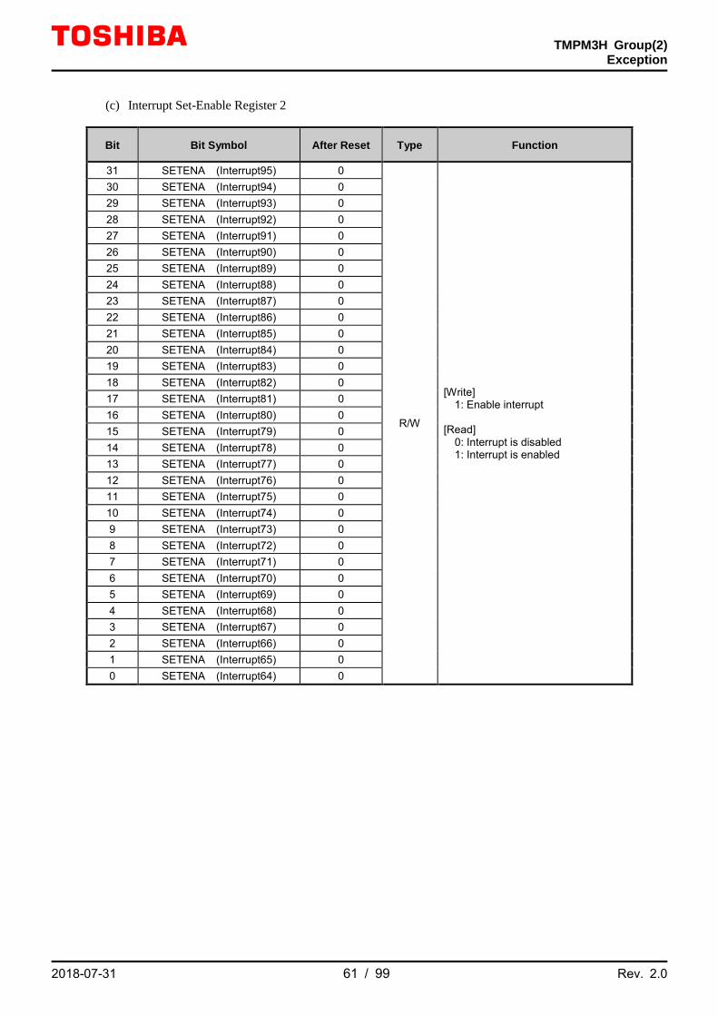
TMPM3H Group(2)
Exception
2018-07-31 61 / 99 Rev. 2.0
(c) Interrupt Set-Enable Register 2
Bit Bit Symbol After Reset Type Function
31 SETENA (Interrupt95) 0
R/W
[Write] 1: Enable interrupt [Read] 0: Interrupt is disabled 1: Interrupt is enabled
30 SETENA (Interrupt94) 0 29 SETENA (Interrupt93) 0 28 SETENA (Interrupt92) 0 27 SETENA (Interrupt91) 0 26 SETENA (Interrupt90) 0 25 SETENA (Interrupt89) 0 24 SETENA (Interrupt88) 0 23 SETENA (Interrupt87) 0 22 SETENA (Interrupt86) 0 21 SETENA (Interrupt85) 0 20 SETENA (Interrupt84) 0 19 SETENA (Interrupt83) 0 18 SETENA (Interrupt82) 0 17 SETENA (Interrupt81) 0 16 SETENA (Interrupt80) 0 15 SETENA (Interrupt79) 0 14 SETENA (Interrupt78) 0 13 SETENA (Interrupt77) 0 12 SETENA (Interrupt76) 0 11 SETENA (Interrupt75) 0 10 SETENA (Interrupt74) 0 9 SETENA (Interrupt73) 0 8 SETENA (Interrupt72) 0 7 SETENA (Interrupt71) 0 6 SETENA (Interrupt70) 0 5 SETENA (Interrupt69) 0 4 SETENA (Interrupt68) 0 3 SETENA (Interrupt67) 0 2 SETENA (Interrupt66) 0 1 SETENA (Interrupt65) 0 0 SETENA (Interrupt64) 0

TMPM3H Group(2)
Exception
2018-07-31 62 / 99 Rev. 2.0
(d) Interrupt Set-Enable Register 3
Bit Bit Symbol After Reset Type Function
31 SETENA (Interrupt127) 0
R/W
[Write] 1: Enable interrupt [Read] 0: Interrupt is disabled 1: Interrupt is enabled
30 SETENA (Interrupt126) 0 29 SETENA (Interrupt125) 0 28 SETENA (Interrupt124) 0 27 SETENA (Interrupt123) 0 26 SETENA (Interrupt122) 0 25 SETENA (Interrupt121) 0 24 SETENA (Interrupt120) 0 23 SETENA (Interrupt119) 0 22 SETENA (Interrupt118) 0 21 SETENA (Interrupt117) 0 20 SETENA (Interrupt116) 0 19 SETENA (Interrupt115) 0 18 SETENA (Interrupt114) 0 17 SETENA (Interrupt113) 0 16 SETENA (Interrupt112) 0 15 SETENA (Interrupt111) 0 14 SETENA (Interrupt110) 0 13 SETENA (Interrupt109) 0 12 SETENA (Interrupt108) 0 11 SETENA (Interrupt107) 0 10 SETENA (Interrupt106) 0 9 SETENA (Interrupt105) 0 8 SETENA (Interrupt104) 0 7 SETENA (Interrupt103) 0 6 SETENA (Interrupt102) 0 5 SETENA (Interrupt101) 0 4 SETENA (Interrupt100) 0 3 SETENA (Interrupt99) 0 2 SETENA (Interrupt98) 0 1 SETENA (Interrupt97) 0 0 SETENA (Interrupt96) 0

TMPM3H Group(2)
Exception
2018-07-31 63 / 99 Rev. 2.0
(e) Interrupt Set-Enable Register 4
Bit Bit Symbol After Reset Type Function
31 SETENA (Interrupt159) 0
R/W
[Write] 1: Enable interrupt [Read] 0: Interrupt is disabled 1: Interrupt is enabled
30 SETENA (Interrupt158) 0 29 SETENA (Interrupt157) 0 28 SETENA (Interrupt156) 0 27 SETENA (Interrupt155) 0 26 SETENA (Interrupt154) 0 25 SETENA (Interrupt153) 0 24 SETENA (Interrupt152) 0 23 SETENA (Interrupt151) 0 22 SETENA (Interrupt150) 0 21 SETENA (Interrupt149) 0 20 SETENA (Interrupt148) 0 19 SETENA (Interrupt147) 0 18 SETENA (Interrupt146) 0 17 SETENA (Interrupt145) 0 16 SETENA (Interrupt144) 0 15 SETENA (Interrupt143) 0 14 SETENA (Interrupt142) 0 13 SETENA (Interrupt141) 0 12 SETENA (Interrupt140) 0 11 SETENA (Interrupt139) 0 10 SETENA (Interrupt138) 0 9 SETENA (Interrupt137) 0 8 SETENA (Interrupt136) 0 7 SETENA (Interrupt135) 0 6 SETENA (Interrupt134) 0 5 SETENA (Interrupt133) 0 4 SETENA (Interrupt132) 0 3 SETENA (Interrupt131) 0 2 SETENA (Interrupt130) 0 1 SETENA (Interrupt129) 0 0 SETENA (Interrupt128) 0

TMPM3H Group(2)
Exception
2018-07-31 64 / 99 Rev. 2.0
(f) Interrupt Set-Enable Register 5
Bit Bit Symbol After Reset Type Function
31:8 - 0 R Read as “0” 7 - 0
R/W Write as “0” 6 - 0 5 SETENA (Interrupt165) 0
R/W
[Write] 1: Enable interrupt [Read] 0: Interrupt is disabled 1: Interrupt is enabled
4 SETENA (Interrupt164) 0 3 SETENA (Interrupt163) 0 2 SETENA (Interrupt162) 0 1 SETENA (Interrupt161) 0 0 SETENA (Interrupt160) 0
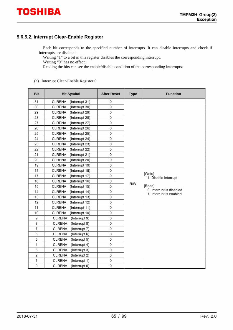
TMPM3H Group(2)
Exception
2018-07-31 65 / 99 Rev. 2.0
5.6.5.2. Interrupt Clear-Enable Register
Each bit corresponds to the specified number of interrupts. It can disable interrupts and check if interrupts are disabled.
Writing “1” to a bit in this register disables the corresponding interrupt. Writing “0” has no effect. Reading the bits can see the enable/disable condition of the corresponding interrupts.
(a) Interrupt Clear-Enable Register 0
Bit Bit Symbol After Reset Type Function
31 CLRENA (Interrupt 31) 0
R/W
[Write] 1: Disable Interrupt [Read] 0: Interrupt is disabled 1: Interrupt is enabled
30 CLRENA (Interrupt 30) 0 29 CLRENA (Interrupt 29) 0 28 CLRENA (Interrupt 28) 0 27 CLRENA (Interrupt 27) 0 26 CLRENA (Interrupt 26) 0 25 CLRENA (Interrupt 25) 0 24 CLRENA (Interrupt 24) 0 23 CLRENA (Interrupt 23) 0 22 CLRENA (Interrupt 22) 0 21 CLRENA (Interrupt 21) 0 20 CLRENA (Interrupt 20) 0 19 CLRENA (Interrupt 19) 0 18 CLRENA (Interrupt 18) 0 17 CLRENA (Interrupt 17) 0 16 CLRENA (Interrupt 16) 0 15 CLRENA (Interrupt 15) 0 14 CLRENA (Interrupt 14) 0 13 CLRENA (Interrupt 13) 0 12 CLRENA (Interrupt 12) 0 11 CLRENA (Interrupt 11) 0 10 CLRENA (Interrupt 10) 0 9 CLRENA (Interrupt 9) 0 8 CLRENA (Interrupt 8) 0 7 CLRENA (Interrupt 7) 0 6 CLRENA (Interrupt 6) 0 5 CLRENA (Interrupt 5) 0 4 CLRENA (Interrupt 4) 0 3 CLRENA (Interrupt 3) 0 2 CLRENA (Interrupt 2) 0 1 CLRENA (Interrupt 1) 0 0 CLRENA (Interrupt 0) 0

TMPM3H Group(2)
Exception
2018-07-31 66 / 99 Rev. 2.0
(b) Interrupt Clear-Enable Register 1
Bit Bit Symbol After Reset Type Function
31 CLRENA (Interrupt 63) 0
R/W
[Write] 1: Disable Interrupt [Read] 0: Interrupt is disabled 1: Interrupt is enabled
30 CLRENA (Interrupt 62) 0 29 CLRENA (Interrupt 61) 0 28 CLRENA (Interrupt 60) 0 27 CLRENA (Interrupt 59) 0 26 CLRENA (Interrupt 58) 0 25 CLRENA (Interrupt 57) 0 24 CLRENA (Interrupt 56) 0 23 CLRENA (Interrupt 55) 0 22 CLRENA (Interrupt 54) 0 21 CLRENA (Interrupt 53) 0 20 CLRENA (Interrupt 52) 0 19 CLRENA (Interrupt 51) 0 18 CLRENA (Interrupt 50) 0 17 CLRENA (Interrupt 49) 0 16 CLRENA (Interrupt 48) 0 15 CLRENA (Interrupt 47) 0 14 CLRENA (Interrupt 46) 0 13 CLRENA (Interrupt 45) 0 12 CLRENA (Interrupt 44) 0 11 CLRENA (Interrupt 43) 0 10 CLRENA (Interrupt 42) 0 9 CLRENA (Interrupt 41) 0 8 CLRENA (Interrupt 40) 0 7 CLRENA (Interrupt 39) 0 6 CLRENA (Interrupt 38) 0 5 CLRENA (Interrupt 37) 0 4 CLRENA (Interrupt 36) 0 3 CLRENA (Interrupt 35) 0 2 CLRENA (Interrupt 34) 0 1 CLRENA (Interrupt 33) 0 0 CLRENA (Interrupt 32) 0
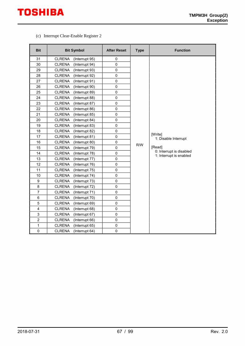
TMPM3H Group(2)
Exception
2018-07-31 67 / 99 Rev. 2.0
(c) Interrupt Clear-Enable Register 2
Bit Bit Symbol After Reset Type Function
31 CLRENA (Interrupt 95) 0
R/W
[Write] 1: Disable Interrupt [Read] 0: Interrupt is disabled 1: Interrupt is enabled
30 CLRENA (Interrupt 94) 0 29 CLRENA (Interrupt 93) 0 28 CLRENA (Interrupt 92) 0 27 CLRENA (Interrupt 91) 0 26 CLRENA (Interrupt 90) 0 25 CLRENA (Interrupt 89) 0 24 CLRENA (Interrupt 88) 0 23 CLRENA (Interrupt 87) 0 22 CLRENA (Interrupt 86) 0 21 CLRENA (Interrupt 85) 0 20 CLRENA (Interrupt 84) 0 19 CLRENA (Interrupt 83) 0 18 CLRENA (Interrupt 82) 0 17 CLRENA (Interrupt 81) 0 16 CLRENA (Interrupt 80) 0 15 CLRENA (Interrupt 79) 0 14 CLRENA (Interrupt 78) 0 13 CLRENA (Interrupt 77) 0 12 CLRENA (Interrupt 76) 0 11 CLRENA (Interrupt 75) 0 10 CLRENA (Interrupt 74) 0 9 CLRENA (Interrupt 73) 0 8 CLRENA (Interrupt 72) 0 7 CLRENA (Interrupt 71) 0 6 CLRENA (Interrupt 70) 0 5 CLRENA (Interrupt 69) 0 4 CLRENA (Interrupt 68) 0 3 CLRENA (Interrupt 67) 0 2 CLRENA (Interrupt 66) 0 1 CLRENA (Interrupt 65) 0 0 CLRENA (Interrupt 64) 0

TMPM3H Group(2)
Exception
2018-07-31 68 / 99 Rev. 2.0
(d) Interrupt Clear-Enable Register 3
Bit Bit Symbol After Reset Type Function
31 CLRENA (Interrupt 127) 0
R/W
[Write] 1: Disable Interrupt [Read] 0: Interrupt is disabled 1: Interrupt is enabled
30 CLRENA (Interrupt 126) 0 29 CLRENA (Interrupt 125) 0 28 CLRENA (Interrupt 124) 0 27 CLRENA (Interrupt 123) 0 26 CLRENA (Interrupt 122) 0 25 CLRENA (Interrupt 121) 0 24 CLRENA (Interrupt 120) 0 23 CLRENA (Interrupt 119) 0 22 CLRENA (Interrupt 118) 0 21 CLRENA (Interrupt 117) 0 20 CLRENA (Interrupt 116) 0 19 CLRENA (Interrupt 115) 0 18 CLRENA (Interrupt 114) 0 17 CLRENA (Interrupt 113) 0 16 CLRENA (Interrupt 112) 0 15 CLRENA (Interrupt 111) 0 14 CLRENA (Interrupt 110) 0 13 CLRENA (Interrupt 109) 0 12 CLRENA (Interrupt 108) 0 11 CLRENA (Interrupt 107) 0 10 CLRENA (Interrupt 106) 0 9 CLRENA (Interrupt 105) 0 8 CLRENA (Interrupt 104) 0 7 CLRENA (Interrupt 103) 0 6 CLRENA (Interrupt 102) 0 5 CLRENA (Interrupt 101) 0 4 CLRENA (Interrupt 100) 0 3 CLRENA (Interrupt 99) 0 2 CLRENA (Interrupt 98) 0 1 CLRENA (Interrupt 97) 0 0 CLRENA (Interrupt 96) 0

TMPM3H Group(2)
Exception
2018-07-31 69 / 99 Rev. 2.0
(e) Interrupt Clear-Enable Register 4
Bit Bit Symbol After Reset Type Function
31 CLRENA (Interrupt 159) 0
R/W
[Write] 1: Disable Interrupt [Read] 0: Interrupt is disabled 1: Interrupt is enabled
30 CLRENA (Interrupt 158) 0 29 CLRENA (Interrupt 157) 0 28 CLRENA (Interrupt 156) 0 27 CLRENA (Interrupt 155) 0 26 CLRENA (Interrupt 154) 0 25 CLRENA (Interrupt 153) 0 24 CLRENA (Interrupt 152) 0 23 CLRENA (Interrupt 151) 0 22 CLRENA (Interrupt 150) 0 21 CLRENA (Interrupt 149) 0 20 CLRENA (Interrupt 148) 0 19 CLRENA (Interrupt 147) 0 18 CLRENA (Interrupt 146) 0 17 CLRENA (Interrupt 145) 0 16 CLRENA (Interrupt 144) 0 15 CLRENA (Interrupt 143) 0 14 CLRENA (Interrupt 142) 0 13 CLRENA (Interrupt 141) 0 12 CLRENA (Interrupt 140) 0 11 CLRENA (Interrupt 139) 0 10 CLRENA (Interrupt 138) 0 9 CLRENA (Interrupt 137) 0 8 CLRENA (Interrupt 136) 0 7 CLRENA (Interrupt 135) 0 6 CLRENA (Interrupt 134) 0 5 CLRENA (Interrupt 133) 0 4 CLRENA (Interrupt 132) 0 3 CLRENA (Interrupt 131) 0 2 CLRENA (Interrupt 130) 0 1 CLRENA (Interrupt 129) 0 0 CLRENA (Interrupt 128) 0
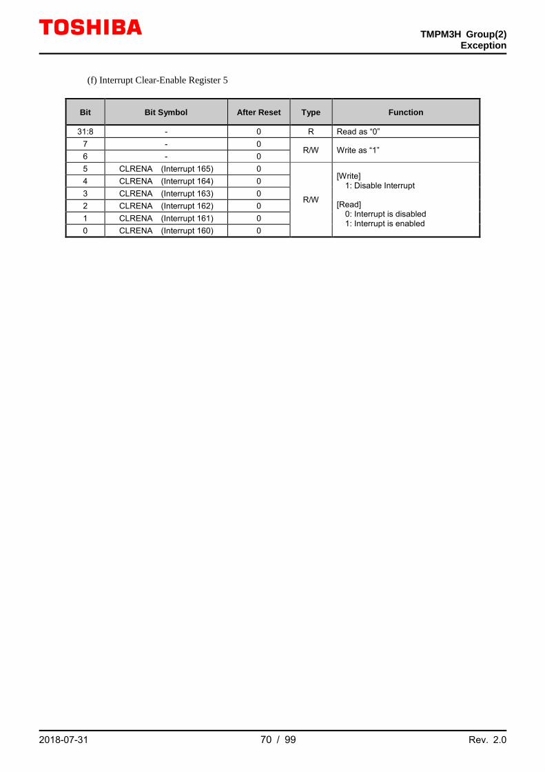
TMPM3H Group(2)
Exception
2018-07-31 70 / 99 Rev. 2.0
(f) Interrupt Clear-Enable Register 5
Bit Bit Symbol After Reset Type Function
31:8 - 0 R Read as “0” 7 - 0
R/W Write as “1” 6 - 0 5 CLRENA (Interrupt 165) 0
R/W
[Write] 1: Disable Interrupt [Read] 0: Interrupt is disabled 1: Interrupt is enabled
4 CLRENA (Interrupt 164) 0 3 CLRENA (Interrupt 163) 0 2 CLRENA (Interrupt 162) 0 1 CLRENA (Interrupt 161) 0 0 CLRENA (Interrupt 160) 0
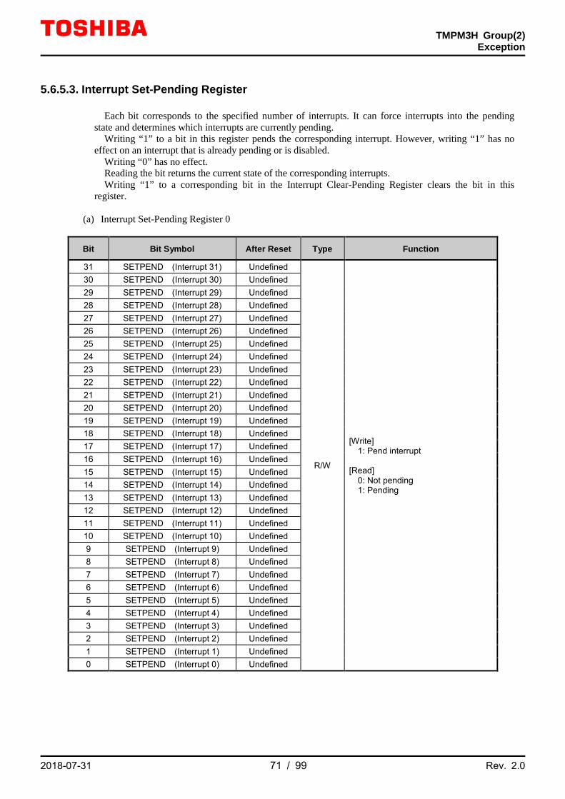
TMPM3H Group(2)
Exception
2018-07-31 71 / 99 Rev. 2.0
5.6.5.3. Interrupt Set-Pending Register
Each bit corresponds to the specified number of interrupts. It can force interrupts into the pending state and determines which interrupts are currently pending.
Writing “1” to a bit in this register pends the corresponding interrupt. However, writing “1” has no effect on an interrupt that is already pending or is disabled.
Writing “0” has no effect. Reading the bit returns the current state of the corresponding interrupts. Writing “1” to a corresponding bit in the Interrupt Clear-Pending Register clears the bit in this
register.
(a) Interrupt Set-Pending Register 0
Bit Bit Symbol After Reset Type Function
31 SETPEND (Interrupt 31) Undefined
R/W
[Write] 1: Pend interrupt [Read] 0: Not pending 1: Pending
30 SETPEND (Interrupt 30) Undefined 29 SETPEND (Interrupt 29) Undefined 28 SETPEND (Interrupt 28) Undefined 27 SETPEND (Interrupt 27) Undefined 26 SETPEND (Interrupt 26) Undefined 25 SETPEND (Interrupt 25) Undefined 24 SETPEND (Interrupt 24) Undefined 23 SETPEND (Interrupt 23) Undefined 22 SETPEND (Interrupt 22) Undefined 21 SETPEND (Interrupt 21) Undefined 20 SETPEND (Interrupt 20) Undefined 19 SETPEND (Interrupt 19) Undefined 18 SETPEND (Interrupt 18) Undefined 17 SETPEND (Interrupt 17) Undefined 16 SETPEND (Interrupt 16) Undefined 15 SETPEND (Interrupt 15) Undefined 14 SETPEND (Interrupt 14) Undefined 13 SETPEND (Interrupt 13) Undefined 12 SETPEND (Interrupt 12) Undefined 11 SETPEND (Interrupt 11) Undefined 10 SETPEND (Interrupt 10) Undefined 9 SETPEND (Interrupt 9) Undefined 8 SETPEND (Interrupt 8) Undefined 7 SETPEND (Interrupt 7) Undefined 6 SETPEND (Interrupt 6) Undefined 5 SETPEND (Interrupt 5) Undefined 4 SETPEND (Interrupt 4) Undefined 3 SETPEND (Interrupt 3) Undefined 2 SETPEND (Interrupt 2) Undefined 1 SETPEND (Interrupt 1) Undefined 0 SETPEND (Interrupt 0) Undefined

TMPM3H Group(2)
Exception
2018-07-31 72 / 99 Rev. 2.0
(b) Interrupt Set-Pending Register 1
Bit Bit Symbol After Reset Type Function
31 SETPEND (Interrupt 63) Undefined
R/W
[Write] 1: Pend interrupt [Read] 0: Not pending 1: Pending
30 SETPEND (Interrupt 62) Undefined 29 SETPEND (Interrupt 61) Undefined 28 SETPEND (Interrupt 60) Undefined 27 SETPEND (Interrupt 59) Undefined 26 SETPEND (Interrupt 58) Undefined 25 SETPEND (Interrupt 57) Undefined 24 SETPEND (Interrupt 56) Undefined 23 SETPEND (Interrupt 55) Undefined 22 SETPEND (Interrupt 54) Undefined 21 SETPEND (Interrupt 53) Undefined 20 SETPEND (Interrupt 52) Undefined 19 SETPEND (Interrupt 51) Undefined 18 SETPEND (Interrupt 50) Undefined 17 SETPEND (Interrupt 49) Undefined 16 SETPEND (Interrupt 48) Undefined 15 SETPEND (Interrupt 47) Undefined 14 SETPEND (Interrupt 46) Undefined 13 SETPEND (Interrupt 45) Undefined 12 SETPEND (Interrupt 44) Undefined 11 SETPEND (Interrupt 43) Undefined 10 SETPEND (Interrupt 42) Undefined 9 SETPEND (Interrupt 41) Undefined 8 SETPEND (Interrupt 40) Undefined 7 SETPEND (Interrupt 39) Undefined 6 SETPEND (Interrupt 38) Undefined 5 SETPEND (Interrupt 37) Undefined 4 SETPEND (Interrupt 36) Undefined 3 SETPEND (Interrupt 35) Undefined 2 SETPEND (Interrupt 34) Undefined 1 SETPEND (Interrupt 33) Undefined 0 SETPEND (Interrupt 32) Undefined

TMPM3H Group(2)
Exception
2018-07-31 73 / 99 Rev. 2.0
(c) Interrupt Set-Pending Register 2
Bit Bit Symbol After Reset Type Function
31 SETPEND (Interrupt 95) Undefined
R/W
[Write] 1: Pend interrupt [Read] 0: Not pending 1: Pending
30 SETPEND (Interrupt 94) Undefined 29 SETPEND (Interrupt 93) Undefined 28 SETPEND (Interrupt 92) Undefined 27 SETPEND (Interrupt 91) Undefined 26 SETPEND (Interrupt 90) Undefined 25 SETPEND (Interrupt 89) Undefined 24 SETPEND (Interrupt 88) Undefined 23 SETPEND (Interrupt 87) Undefined 22 SETPEND (Interrupt 86) Undefined 21 SETPEND (Interrupt 85) Undefined 20 SETPEND (Interrupt 84) Undefined 19 SETPEND (Interrupt 83) Undefined 18 SETPEND (Interrupt 82) Undefined 17 SETPEND (Interrupt 81) Undefined 16 SETPEND (Interrupt 80) Undefined 15 SETPEND (Interrupt 79) Undefined 14 SETPEND (Interrupt 78) Undefined 13 SETPEND (Interrupt 77) Undefined 12 SETPEND (Interrupt 76) Undefined 11 SETPEND (Interrupt 75) Undefined 10 SETPEND (Interrupt 74) Undefined 9 SETPEND (Interrupt 73) Undefined 8 SETPEND (Interrupt 72) Undefined 7 SETPEND (Interrupt 71) Undefined 6 SETPEND (Interrupt 70) Undefined 5 SETPEND (Interrupt 69) Undefined 4 SETPEND (Interrupt 68) Undefined 3 SETPEND (Interrupt 67) Undefined 2 SETPEND (Interrupt 66) Undefined 1 SETPEND (Interrupt 65) Undefined 0 SETPEND (Interrupt 64) Undefined

TMPM3H Group(2)
Exception
2018-07-31 74 / 99 Rev. 2.0
(d) Interrupt Set-Pending Register 3
Bit Bit Symbol After Reset Type Function
31 SETPEND (Interrupt 127) Undefined
R/W
[Write] 1: Pend interrupt [Read] 0: Not pending 1: Pending
30 SETPEND (Interrupt 126) Undefined 29 SETPEND (Interrupt 125) Undefined 28 SETPEND (Interrupt 124) Undefined 27 SETPEND (Interrupt 123) Undefined 26 SETPEND (Interrupt 122) Undefined 25 SETPEND (Interrupt 121) Undefined 24 SETPEND (Interrupt 120) Undefined 23 SETPEND (Interrupt 119) Undefined 22 SETPEND (Interrupt 118) Undefined 21 SETPEND (Interrupt 117) Undefined 20 SETPEND (Interrupt 116) Undefined 19 SETPEND (Interrupt 115) Undefined 18 SETPEND (Interrupt 114) Undefined 17 SETPEND (Interrupt 113) Undefined 16 SETPEND (Interrupt 112) Undefined 15 SETPEND (Interrupt 111) Undefined 14 SETPEND (Interrupt 110) Undefined 13 SETPEND (Interrupt 109) Undefined 12 SETPEND (Interrupt 108) Undefined 11 SETPEND (Interrupt 107) Undefined 10 SETPEND (Interrupt 106) Undefined 9 SETPEND (Interrupt 105) Undefined 8 SETPEND (Interrupt 104) Undefined 7 SETPEND (Interrupt 103) Undefined 6 SETPEND (Interrupt 102) Undefined 5 SETPEND (Interrupt 101) Undefined 4 SETPEND (Interrupt 100) Undefined 3 SETPEND (Interrupt 99) Undefined 2 SETPEND (Interrupt 98) Undefined 1 SETPEND (Interrupt 97) Undefined 0 SETPEND (Interrupt 96) Undefined

TMPM3H Group(2)
Exception
2018-07-31 75 / 99 Rev. 2.0
(e) Interrupt Set-Pending Register 4
Bit Bit Symbol After Reset Type Function
31 SETPEND (Interrupt 159) Undefined
R/W
[Write] 1: Pend interrupt [Read] 0: Not pending 1: Pending
30 SETPEND (Interrupt 158) Undefined 29 SETPEND (Interrupt 157) Undefined 28 SETPEND (Interrupt 156) Undefined 27 SETPEND (Interrupt 155) Undefined 26 SETPEND (Interrupt 154) Undefined 25 SETPEND (Interrupt 153) Undefined 24 SETPEND (Interrupt 152) Undefined 23 SETPEND (Interrupt 151) Undefined 22 SETPEND (Interrupt 150) Undefined 21 SETPEND (Interrupt 149) Undefined 20 SETPEND (Interrupt 148) Undefined 19 SETPEND (Interrupt 147) Undefined 18 SETPEND (Interrupt 146) Undefined 17 SETPEND (Interrupt 145) Undefined 16 SETPEND (Interrupt 144) Undefined 15 SETPEND (Interrupt 143) Undefined 14 SETPEND (Interrupt 142) Undefined 13 SETPEND (Interrupt 141) Undefined 12 SETPEND (Interrupt 140) Undefined 11 SETPEND (Interrupt 139) Undefined 10 SETPEND (Interrupt 138) Undefined 9 SETPEND (Interrupt 137) Undefined 8 SETPEND (Interrupt 136) Undefined 7 SETPEND (Interrupt 135) Undefined 6 SETPEND (Interrupt 134) Undefined 5 SETPEND (Interrupt 133) Undefined 4 SETPEND (Interrupt 132) Undefined 3 SETPEND (Interrupt 131) Undefined 2 SETPEND (Interrupt 130) Undefined 1 SETPEND (Interrupt 129) Undefined 0 SETPEND (Interrupt 128) Undefined
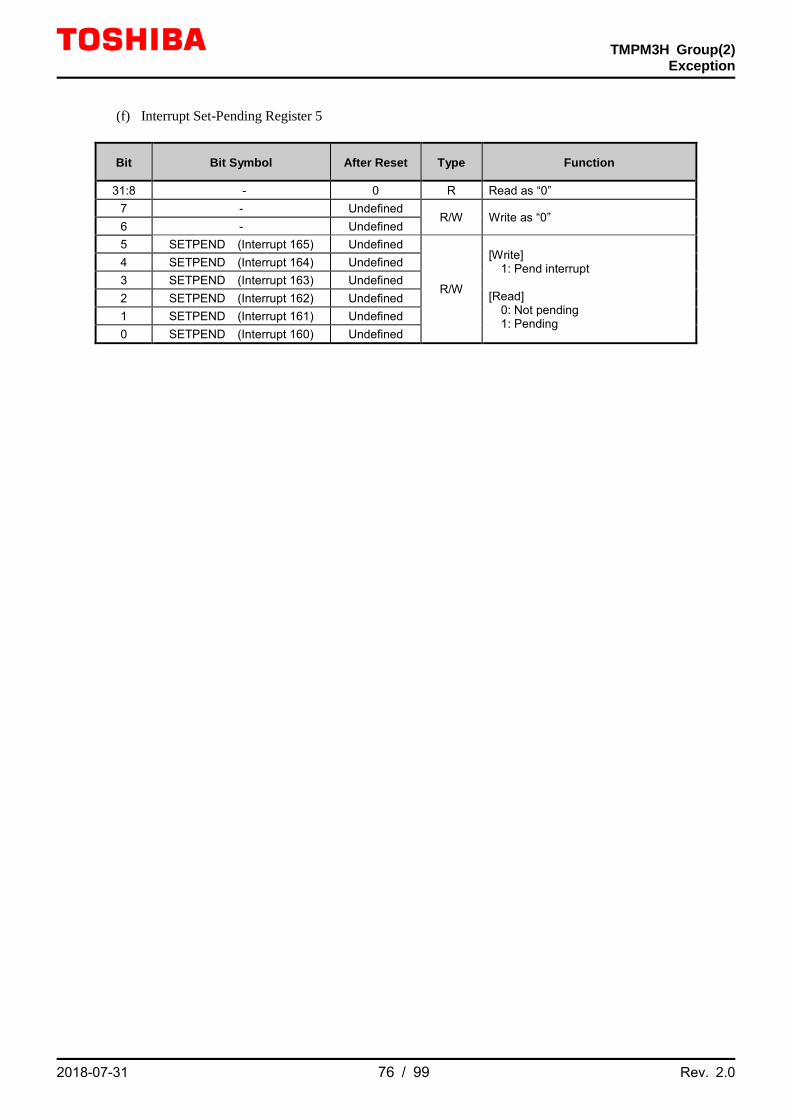
TMPM3H Group(2)
Exception
2018-07-31 76 / 99 Rev. 2.0
(f) Interrupt Set-Pending Register 5
Bit Bit Symbol After Reset Type Function
31:8 - 0 R Read as “0” 7 - Undefined
R/W Write as “0” 6 - Undefined 5 SETPEND (Interrupt 165) Undefined
R/W
[Write] 1: Pend interrupt [Read] 0: Not pending 1: Pending
4 SETPEND (Interrupt 164) Undefined 3 SETPEND (Interrupt 163) Undefined 2 SETPEND (Interrupt 162) Undefined 1 SETPEND (Interrupt 161) Undefined 0 SETPEND (Interrupt 160) Undefined
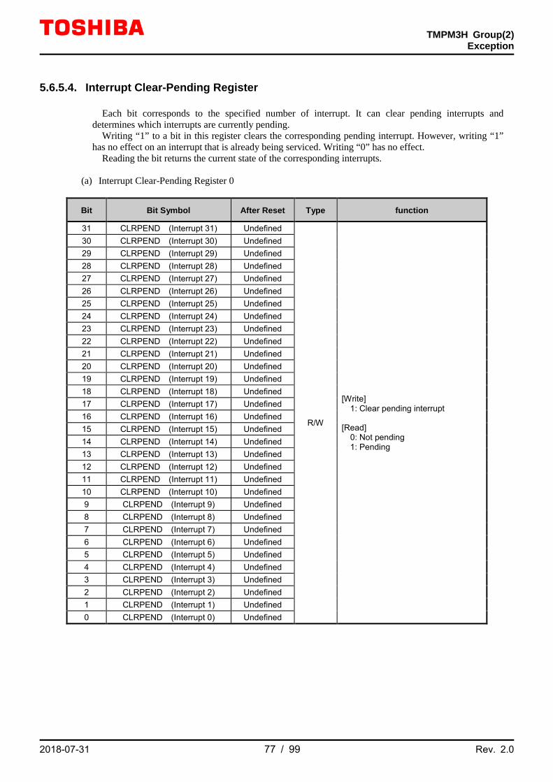
TMPM3H Group(2)
Exception
2018-07-31 77 / 99 Rev. 2.0
5.6.5.4. Interrupt Clear-Pending Register
Each bit corresponds to the specified number of interrupt. It can clear pending interrupts and determines which interrupts are currently pending.
Writing “1” to a bit in this register clears the corresponding pending interrupt. However, writing “1” has no effect on an interrupt that is already being serviced. Writing “0” has no effect.
Reading the bit returns the current state of the corresponding interrupts.
(a) Interrupt Clear-Pending Register 0
Bit Bit Symbol After Reset Type function
31 CLRPEND (Interrupt 31) Undefined
R/W
[Write] 1: Clear pending interrupt [Read] 0: Not pending 1: Pending
30 CLRPEND (Interrupt 30) Undefined 29 CLRPEND (Interrupt 29) Undefined 28 CLRPEND (Interrupt 28) Undefined 27 CLRPEND (Interrupt 27) Undefined 26 CLRPEND (Interrupt 26) Undefined 25 CLRPEND (Interrupt 25) Undefined 24 CLRPEND (Interrupt 24) Undefined 23 CLRPEND (Interrupt 23) Undefined 22 CLRPEND (Interrupt 22) Undefined 21 CLRPEND (Interrupt 21) Undefined 20 CLRPEND (Interrupt 20) Undefined 19 CLRPEND (Interrupt 19) Undefined 18 CLRPEND (Interrupt 18) Undefined 17 CLRPEND (Interrupt 17) Undefined 16 CLRPEND (Interrupt 16) Undefined 15 CLRPEND (Interrupt 15) Undefined 14 CLRPEND (Interrupt 14) Undefined 13 CLRPEND (Interrupt 13) Undefined 12 CLRPEND (Interrupt 12) Undefined 11 CLRPEND (Interrupt 11) Undefined 10 CLRPEND (Interrupt 10) Undefined 9 CLRPEND (Interrupt 9) Undefined 8 CLRPEND (Interrupt 8) Undefined 7 CLRPEND (Interrupt 7) Undefined 6 CLRPEND (Interrupt 6) Undefined 5 CLRPEND (Interrupt 5) Undefined 4 CLRPEND (Interrupt 4) Undefined 3 CLRPEND (Interrupt 3) Undefined 2 CLRPEND (Interrupt 2) Undefined 1 CLRPEND (Interrupt 1) Undefined 0 CLRPEND (Interrupt 0) Undefined

TMPM3H Group(2)
Exception
2018-07-31 78 / 99 Rev. 2.0
(b) Interrupt Clear-Pending Register 1
Bit Bit Symbol After Reset Type Function
31 CLRPEND (Interrupt 63) Undefined
R/W
[Write] 1: Clear pending interrupt [Read] 0: Not pending 1: Pending
30 CLRPEND (Interrupt 62) Undefined 29 CLRPEND (Interrupt 61) Undefined 28 CLRPEND (Interrupt 60) Undefined 27 CLRPEND (Interrupt 59) Undefined 26 CLRPEND (Interrupt 58) Undefined 25 CLRPEND (Interrupt 57) Undefined 24 CLRPEND (Interrupt 56) Undefined 23 CLRPEND (Interrupt 55) Undefined 22 CLRPEND (Interrupt 54) Undefined 21 CLRPEND (Interrupt 53) Undefined 20 CLRPEND (Interrupt 52) Undefined 19 CLRPEND (Interrupt 51) Undefined 18 CLRPEND (Interrupt 50) Undefined 17 CLRPEND (Interrupt 49) Undefined 16 CLRPEND (Interrupt 48) Undefined 15 CLRPEND (Interrupt 47) Undefined 14 CLRPEND (Interrupt 46) Undefined 13 CLRPEND (Interrupt 45) Undefined 12 CLRPEND (Interrupt 44) Undefined 11 CLRPEND (Interrupt 43) Undefined 10 CLRPEND (Interrupt 42) Undefined 9 CLRPEND (Interrupt 41) Undefined 8 CLRPEND (Interrupt 40) Undefined 7 CLRPEND (Interrupt 39) Undefined 6 CLRPEND (Interrupt 38) Undefined 5 CLRPEND (Interrupt 37) Undefined 4 CLRPEND (Interrupt 36) Undefined 3 CLRPEND (Interrupt 35) Undefined 2 CLRPEND (Interrupt 34) Undefined 1 CLRPEND (Interrupt 33) Undefined 0 CLRPEND (Interrupt 32) Undefined

TMPM3H Group(2)
Exception
2018-07-31 79 / 99 Rev. 2.0
(c) Interrupt Clear-Pending Register 2
Bit Bit Symbol After Reset Type Function
31 CLRPEND (Interrupt 95) Undefined
R/W
[Write] 1: Clear pending interrupt [Read] 0: Not pending 1: Pending
30 CLRPEND (Interrupt 94) Undefined 29 CLRPEND (Interrupt 93) Undefined 28 CLRPEND (Interrupt 92) Undefined 27 CLRPEND (Interrupt 91) Undefined 26 CLRPEND (Interrupt 90) Undefined 25 CLRPEND (Interrupt 89) Undefined 24 CLRPEND (Interrupt 88) Undefined 23 CLRPEND (Interrupt 87) Undefined 22 CLRPEND (Interrupt 86) Undefined 21 CLRPEND (Interrupt 85) Undefined 20 CLRPEND (Interrupt 84) Undefined 19 CLRPEND (Interrupt 83) Undefined 18 CLRPEND (Interrupt 82) Undefined 17 CLRPEND (Interrupt 81) Undefined 16 CLRPEND (Interrupt 80) Undefined 15 CLRPEND (Interrupt 79) Undefined 14 CLRPEND (Interrupt 78) Undefined 13 CLRPEND (Interrupt 77) Undefined 12 CLRPEND (Interrupt 76) Undefined 11 CLRPEND (Interrupt 75) Undefined 10 CLRPEND (Interrupt 74) Undefined 9 CLRPEND (Interrupt 73) Undefined 8 CLRPEND (Interrupt 72) Undefined 7 CLRPEND (Interrupt 71) Undefined 6 CLRPEND (Interrupt 70) Undefined 5 CLRPEND (Interrupt 69) Undefined 4 CLRPEND (Interrupt 68) Undefined 3 CLRPEND (Interrupt 67) Undefined 2 CLRPEND (Interrupt 66) Undefined 1 CLRPEND (Interrupt 65) Undefined 0 CLRPEND (Interrupt 64) Undefined

TMPM3H Group(2)
Exception
2018-07-31 80 / 99 Rev. 2.0
(d) Interrupt Clear-Pending Register 3
Bit Bit Symbol After Reset Type Function
31 CLRPEND (Interrupt 127) Undefined
R/W
[Write] 1: Clear pending interrupt [Read] 0: Not pending 1: Pending
30 CLRPEND (Interrupt 126) Undefined 29 CLRPEND (Interrupt 125) Undefined 28 CLRPEND (Interrupt 124) Undefined 27 CLRPEND (Interrupt 123) Undefined 26 CLRPEND (Interrupt 122) Undefined 25 CLRPEND (Interrupt 121) Undefined 24 CLRPEND (Interrupt 120) Undefined 23 CLRPEND (Interrupt 119) Undefined 22 CLRPEND (Interrupt 118) Undefined 21 CLRPEND (Interrupt 117) Undefined 20 CLRPEND (Interrupt 116) Undefined 19 CLRPEND (Interrupt 115) Undefined 18 CLRPEND (Interrupt 114) Undefined 17 CLRPEND (Interrupt 113) Undefined 16 CLRPEND (Interrupt 112) Undefined 15 CLRPEND (Interrupt 111) Undefined 14 CLRPEND (Interrupt 110) Undefined 13 CLRPEND (Interrupt 109) Undefined 12 CLRPEND (Interrupt 108) Undefined 11 CLRPEND (Interrupt 107) Undefined 10 CLRPEND (Interrupt 106) Undefined 9 CLRPEND (Interrupt 105) Undefined 8 CLRPEND (Interrupt 104) Undefined 7 CLRPEND (Interrupt 103) Undefined 6 CLRPEND (Interrupt 102) Undefined 5 CLRPEND (Interrupt 101) Undefined 4 CLRPEND (Interrupt 100) Undefined 3 CLRPEND (Interrupt 99) Undefined 2 CLRPEND (Interrupt 98) Undefined 1 CLRPEND (Interrupt 97) Undefined 0 CLRPEND (Interrupt 96) Undefined
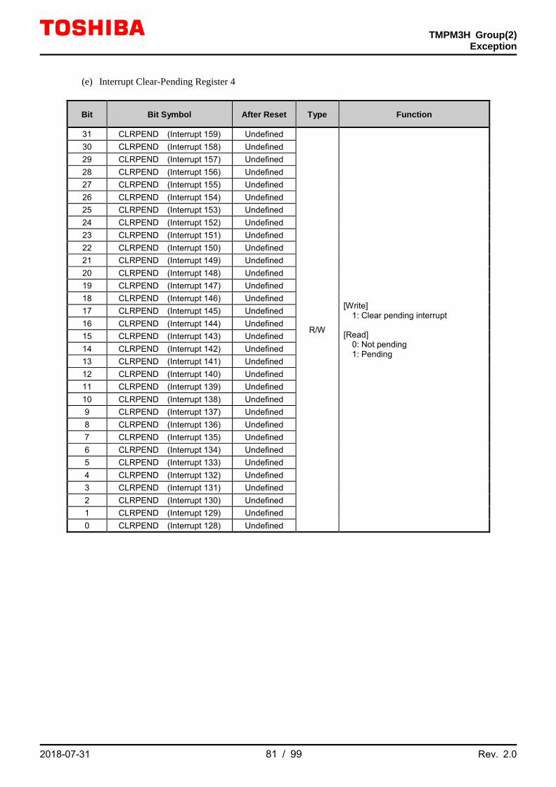
TMPM3H Group(2)
Exception
2018-07-31 81 / 99 Rev. 2.0
(e) Interrupt Clear-Pending Register 4
Bit Bit Symbol After Reset Type Function
31 CLRPEND (Interrupt 159) Undefined
R/W
[Write] 1: Clear pending interrupt [Read] 0: Not pending 1: Pending
30 CLRPEND (Interrupt 158) Undefined 29 CLRPEND (Interrupt 157) Undefined 28 CLRPEND (Interrupt 156) Undefined 27 CLRPEND (Interrupt 155) Undefined 26 CLRPEND (Interrupt 154) Undefined 25 CLRPEND (Interrupt 153) Undefined 24 CLRPEND (Interrupt 152) Undefined 23 CLRPEND (Interrupt 151) Undefined 22 CLRPEND (Interrupt 150) Undefined 21 CLRPEND (Interrupt 149) Undefined 20 CLRPEND (Interrupt 148) Undefined 19 CLRPEND (Interrupt 147) Undefined 18 CLRPEND (Interrupt 146) Undefined 17 CLRPEND (Interrupt 145) Undefined 16 CLRPEND (Interrupt 144) Undefined 15 CLRPEND (Interrupt 143) Undefined 14 CLRPEND (Interrupt 142) Undefined 13 CLRPEND (Interrupt 141) Undefined 12 CLRPEND (Interrupt 140) Undefined 11 CLRPEND (Interrupt 139) Undefined 10 CLRPEND (Interrupt 138) Undefined 9 CLRPEND (Interrupt 137) Undefined 8 CLRPEND (Interrupt 136) Undefined 7 CLRPEND (Interrupt 135) Undefined 6 CLRPEND (Interrupt 134) Undefined 5 CLRPEND (Interrupt 133) Undefined 4 CLRPEND (Interrupt 132) Undefined 3 CLRPEND (Interrupt 131) Undefined 2 CLRPEND (Interrupt 130) Undefined 1 CLRPEND (Interrupt 129) Undefined 0 CLRPEND (Interrupt 128) Undefined
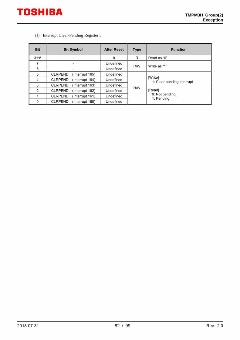
TMPM3H Group(2)
Exception
2018-07-31 82 / 99 Rev. 2.0
(f) Interrupt Clear-Pending Register 5
Bit Bit Symbol After Reset Type Function
31:8 - 0 R Read as “0” 7 - Undefined
R/W Write as “1” 6 - Undefined 5 CLRPEND (Interrupt 165) Undefined
R/W
[Write] 1: Clear pending interrupt [Read] 0: Not pending 1: Pending
4 CLRPEND (Interrupt 164) Undefined 3 CLRPEND (Interrupt 163) Undefined 2 CLRPEND (Interrupt 162) Undefined 1 CLRPEND (Interrupt 161) Undefined 0 CLRPEND (Interrupt 160) Undefined
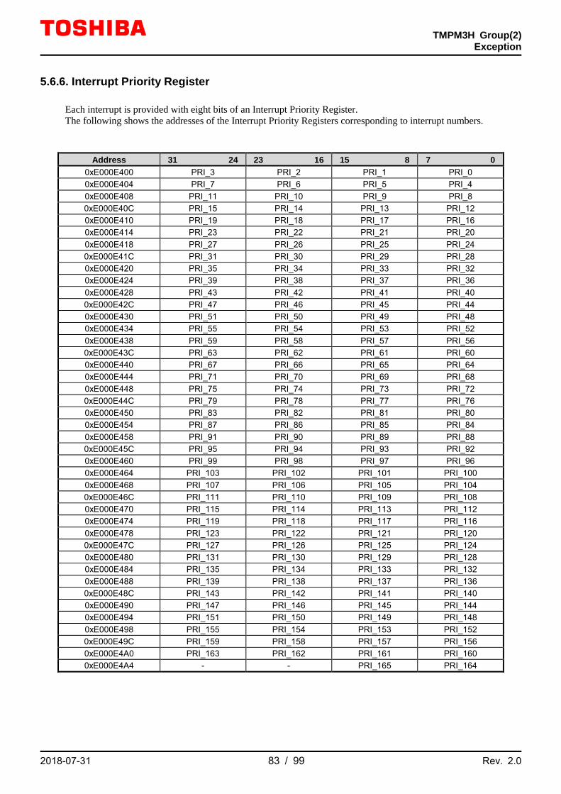
TMPM3H Group(2)
Exception
2018-07-31 83 / 99 Rev. 2.0
5.6.6. Interrupt Priority Register Each interrupt is provided with eight bits of an Interrupt Priority Register. The following shows the addresses of the Interrupt Priority Registers corresponding to interrupt numbers.
Address 31 24 23 16 15 8 7 0 0xE000E400 PRI_3 PRI_2 PRI_1 PRI_0 0xE000E404 PRI_7 PRI_6 PRI_5 PRI_4 0xE000E408 PRI_11 PRI_10 PRI_9 PRI_8 0xE000E40C PRI_15 PRI_14 PRI_13 PRI_12 0xE000E410 PRI_19 PRI_18 PRI_17 PRI_16 0xE000E414 PRI_23 PRI_22 PRI_21 PRI_20 0xE000E418 PRI_27 PRI_26 PRI_25 PRI_24 0xE000E41C PRI_31 PRI_30 PRI_29 PRI_28 0xE000E420 PRI_35 PRI_34 PRI_33 PRI_32 0xE000E424 PRI_39 PRI_38 PRI_37 PRI_36 0xE000E428 PRI_43 PRI_42 PRI_41 PRI_40 0xE000E42C PRI_47 PRI_46 PRI_45 PRI_44 0xE000E430 PRI_51 PRI_50 PRI_49 PRI_48 0xE000E434 PRI_55 PRI_54 PRI_53 PRI_52 0xE000E438 PRI_59 PRI_58 PRI_57 PRI_56 0xE000E43C PRI_63 PRI_62 PRI_61 PRI_60 0xE000E440 PRI_67 PRI_66 PRI_65 PRI_64 0xE000E444 PRI_71 PRI_70 PRI_69 PRI_68 0xE000E448 PRI_75 PRI_74 PRI_73 PRI_72 0xE000E44C PRI_79 PRI_78 PRI_77 PRI_76 0xE000E450 PRI_83 PRI_82 PRI_81 PRI_80 0xE000E454 PRI_87 PRI_86 PRI_85 PRI_84 0xE000E458 PRI_91 PRI_90 PRI_89 PRI_88 0xE000E45C PRI_95 PRI_94 PRI_93 PRI_92 0xE000E460 PRI_99 PRI_98 PRI_97 PRI_96 0xE000E464 PRI_103 PRI_102 PRI_101 PRI_100 0xE000E468 PRI_107 PRI_106 PRI_105 PRI_104 0xE000E46C PRI_111 PRI_110 PRI_109 PRI_108 0xE000E470 PRI_115 PRI_114 PRI_113 PRI_112 0xE000E474 PRI_119 PRI_118 PRI_117 PRI_116 0xE000E478 PRI_123 PRI_122 PRI_121 PRI_120 0xE000E47C PRI_127 PRI_126 PRI_125 PRI_124 0xE000E480 PRI_131 PRI_130 PRI_129 PRI_128 0xE000E484 PRI_135 PRI_134 PRI_133 PRI_132 0xE000E488 PRI_139 PRI_138 PRI_137 PRI_136 0xE000E48C PRI_143 PRI_142 PRI_141 PRI_140 0xE000E490 PRI_147 PRI_146 PRI_145 PRI_144 0xE000E494 PRI_151 PRI_150 PRI_149 PRI_148 0xE000E498 PRI_155 PRI_154 PRI_153 PRI_152 0xE000E49C PRI_159 PRI_158 PRI_157 PRI_156 0xE000E4A0 PRI_163 PRI_162 PRI_161 PRI_160 0xE000E4A4 - - PRI_165 PRI_164
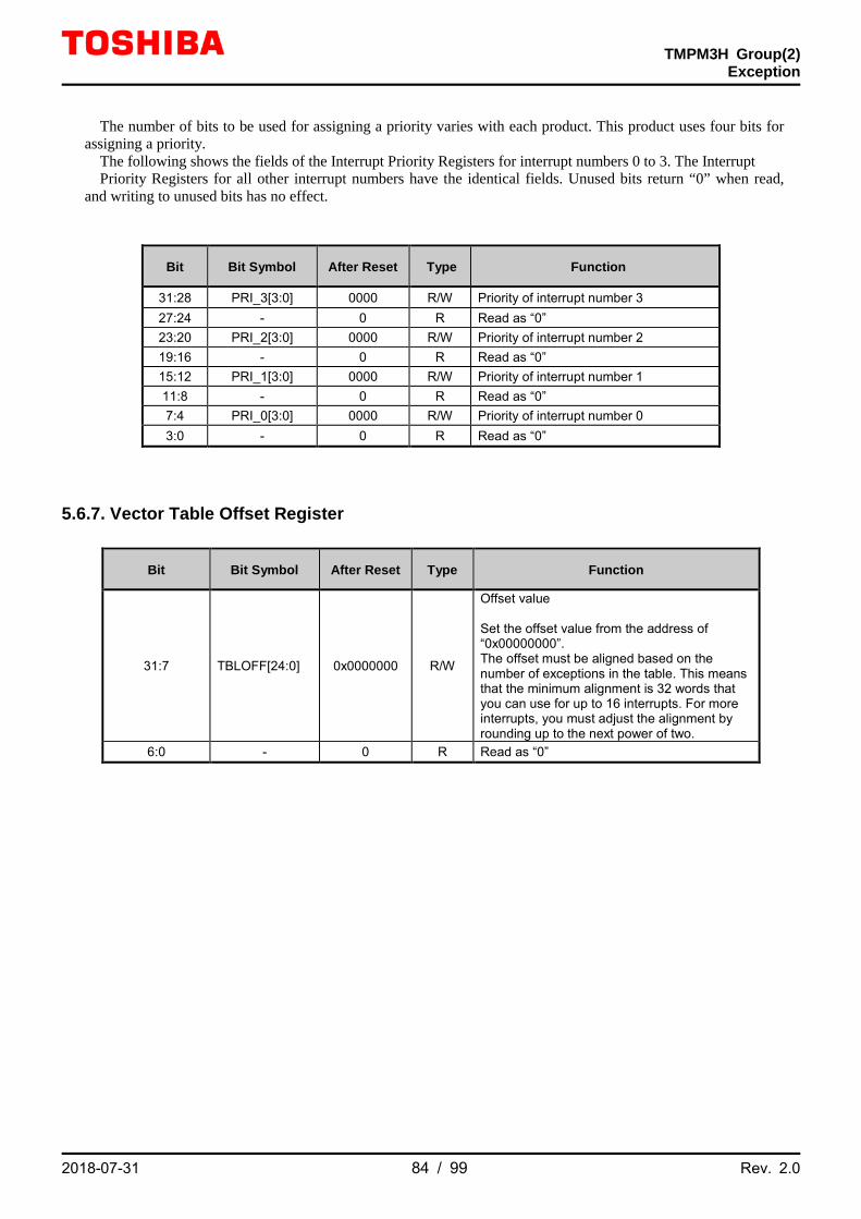
TMPM3H Group(2)
Exception
2018-07-31 84 / 99 Rev. 2.0
The number of bits to be used for assigning a priority varies with each product. This product uses four bits for
assigning a priority. The following shows the fields of the Interrupt Priority Registers for interrupt numbers 0 to 3. The Interrupt Priority Registers for all other interrupt numbers have the identical fields. Unused bits return “0” when read,
and writing to unused bits has no effect.
Bit Bit Symbol After Reset Type Function
31:28 PRI_3[3:0] 0000 R/W Priority of interrupt number 3 27:24 - 0 R Read as “0” 23:20 PRI_2[3:0] 0000 R/W Priority of interrupt number 2 19:16 - 0 R Read as “0” 15:12 PRI_1[3:0] 0000 R/W Priority of interrupt number 1 11:8 - 0 R Read as “0” 7:4 PRI_0[3:0] 0000 R/W Priority of interrupt number 0 3:0 - 0 R Read as “0”
5.6.7. Vector Table Offset Register
Bit Bit Symbol After Reset Type Function
31:7 TBLOFF[24:0] 0x0000000 R/W
Offset value Set the offset value from the address of “0x00000000”. The offset must be aligned based on the number of exceptions in the table. This means that the minimum alignment is 32 words that you can use for up to 16 interrupts. For more interrupts, you must adjust the alignment by rounding up to the next power of two.
6:0 - 0 R Read as “0”
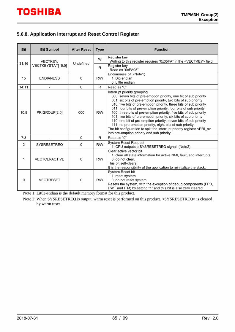
TMPM3H Group(2)
Exception
2018-07-31 85 / 99 Rev. 2.0
5.6.8. Application Interrupt and Reset Control Register
Bit Bit Symbol After Reset Type Function
31:16 VECTKEY/ VECTKEYSTAT[15:0] Undefined
W Register key Writing to this register requires “0x05FA” in the <VECTKEY> field.
R Register key Read as “0xFA05”
15 ENDIANESS 0 R/W Endianness bit: (Note1) 1: Big endian 0: Little endian
14:11 - 0 R Read as “0”
10:8 PRIGROUP[2:0] 000 R/W
Interrupt priority grouping 000: seven bits of pre-emption priority, one bit of sub priority 001: six bits of pre-emption priority, two bits of sub priority 010: five bits of pre-emption priority, three bits of sub priority 011: four bits of pre-emption priority, four bits of sub priority 100: three bits of pre-emption priority, five bits of sub priority 101: two bits of pre-emption priority, six bits of sub priority 110: one bit of pre-emption priority, seven bits of sub priority 111: no pre-emption priority, eight bits of sub priority The bit configuration to split the interrupt priority register <PRI_n> into pre-emption priority and sub priority.
7:3 - 0 R Read as “0”
2 SYSRESETREQ 0 R/W System Reset Request 1: CPU outputs a SYSRESETREQ signal. (Note2)
1 VECTCLRACTIVE 0 R/W
Clear active vector bit 1: clear all state information for active NMI, fault, and interrupts. 0: do not clear. This bit self-clears. It is the responsibility of the application to reinitialize the stack.
0 VECTRESET 0 R/W
System Reset bit 1: reset system. 0: do not reset system. Resets the system, with the exception of debug components (FPB, DWT and ITM) by setting “1” and this bit is also zero cleared
Note 1: Little-endian is the default memory format for this product. Note 2: When SYSRESETREQ is output, warm reset is performed on this product. <SYSRESETREQ> is cleared
by warm reset.

TMPM3H Group(2)
Exception
2018-07-31 86 / 99 Rev. 2.0
5.6.9. System Handler Priority Register Each exception is provided with eight bits of a System Handler Priority Register. The following shows the addresses of the System Handler Priority Registers corresponding to each exception.
Address 31 24 23 16 15 8 7 0
0xE000ED18 PRI_7
PRI_6 (Usage Fault)
PRI_5 (Bus Fault)
PRI_4 (Memory
Management)
0xE000ED1C PRI_11 (SVCall ) PRI_10 PRI_9 PRI_8
0xE000ED20 PRI_15 (SysTick)
PRI_14 (PendSV) PRI_13 PRI_12
(Debug Monitor)
The number of bits to be used for assigning a priority varies with each product. This product uses four bits for
assigning a priority. The following shows the fields of the System Handler Priority Registers for Usage Fault, Bus Fault , and
Memory Management. Unused bits return “0” when read, and writing to unused bits has no effect.
Bit Bit Symbol After Reset Type Function
31:28 PRI_7[3:0] 0000 R/W Reserved 27:24 - 0 R Read as “0” 23:20 PRI_6[3:0] 0000 R/W Priority of Usage Fault 19:16 - 0 R Read as “0” 15:12 PRI_5[3:0] 0000 R/W Priority of Bus Fault 11:8 - 0 R Read as “0” 7:4 PRI_4[3:0] 0000 R/W Priority of Memory Management 3:0 - 0 R Read as “0”

TMPM3H Group(2)
Exception
2018-07-31 87 / 99 Rev. 2.0
5.6.10. System Handler Control and State Register
Bit Bit Symbol After Reset Type Function
31:19 - 0 R Read as “0”
18 USGFAULTENA 0 R/W Usage Fault 0: Disabled 1: Enabled
17 BUSFAULTENA 0 R/W Bus Fault 0: Disabled 1: Enabled
16 MEMFAULTENA 0 R/W Memory Management 0: Disabled 1: Enabled
15 SVCALLPENDED 0 R/W SVCall 0: Not pended 1: Pended
14 BUSFAULTPENDED 0 R/W Bus Fault 0: Not pended 1: Pended
13 MEMFAULTPENDED 0 R/W Memory Management 0: Not pended 1: Pended
12 USGFAULTPENDED 0 R/W Usage fault 0: Not pended 1: Pended
11 SYSTICKACT 0 R/W SysTick 0: Inactive 1: Active
10 PENDSVACT 0 R/W PendSV 0: Inactive 1: Active
9 - 0 R Read as “0”
8 MONITORACT 0 R/W Debug Monitor 0: Inactive 1: Active
7 SVCALLACT 0 R/W SVCall 0: Inactive 1: Active
6:4 - 0 R Read as “0”
3 USGFAULTACT 0 R/W Usage Fault 0: Inactive 1: Active
2 - 0 R Read as “0”
1 BUSFAULTACT 0 R/W Bus Fault 0: Inactive 1: Active
0 MEMFAULTACT 0 R/W Memory Management 0: Inactive 1: Active
Note: You must clear or set the active bits with extreme caution because clearing and setting these bits does not repair stack contents.
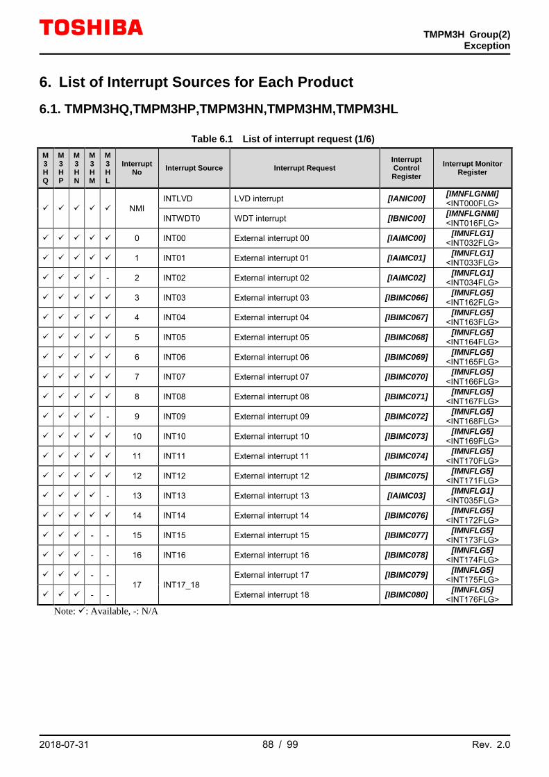
TMPM3H Group(2)
Exception
2018-07-31 88 / 99 Rev. 2.0
6. List of Interrupt Sources for Each Product
6.1. TMPM3HQ,TMPM3HP,TMPM3HN,TMPM3HM,TMPM3HL
Table 6.1 List of interrupt request (1/6) M 3 H Q
M 3 H P
M 3 H N
M 3 H M
M3HL
Interrupt No Interrupt Source Interrupt Request
Interrupt Control Register
Interrupt Monitor Register
NMI INTLVD LVD interrupt [IANIC00] [IMNFLGNMI]
<INT000FLG>
INTWDT0 WDT interrupt [IBNIC00] [IMNFLGNMI] <INT016FLG>
0 INT00 External interrupt 00 [IAIMC00] [IMNFLG1] <INT032FLG>
1 INT01 External interrupt 01 [IAIMC01] [IMNFLG1] <INT033FLG>
- 2 INT02 External interrupt 02 [IAIMC02] [IMNFLG1] <INT034FLG>
3 INT03 External interrupt 03 [IBIMC066] [IMNFLG5] <INT162FLG>
4 INT04 External interrupt 04 [IBIMC067] [IMNFLG5] <INT163FLG>
5 INT05 External interrupt 05 [IBIMC068] [IMNFLG5] <INT164FLG>
6 INT06 External interrupt 06 [IBIMC069] [IMNFLG5] <INT165FLG>
7 INT07 External interrupt 07 [IBIMC070] [IMNFLG5] <INT166FLG>
8 INT08 External interrupt 08 [IBIMC071] [IMNFLG5] <INT167FLG>
- 9 INT09 External interrupt 09 [IBIMC072] [IMNFLG5] <INT168FLG>
10 INT10 External interrupt 10 [IBIMC073] [IMNFLG5] <INT169FLG>
11 INT11 External interrupt 11 [IBIMC074] [IMNFLG5] <INT170FLG>
12 INT12 External interrupt 12 [IBIMC075] [IMNFLG5] <INT171FLG>
- 13 INT13 External interrupt 13 [IAIMC03] [IMNFLG1] <INT035FLG>
14 INT14 External interrupt 14 [IBIMC076] [IMNFLG5] <INT172FLG>
- - 15 INT15 External interrupt 15 [IBIMC077] [IMNFLG5] <INT173FLG>
- - 16 INT16 External interrupt 16 [IBIMC078] [IMNFLG5] <INT174FLG>
- - 17 INT17_18
External interrupt 17 [IBIMC079] [IMNFLG5] <INT175FLG>
- - External interrupt 18 [IBIMC080] [IMNFLG5] <INT176FLG>
Note: : Available, -: N/A

TMPM3H Group(2)
Exception
2018-07-31 89 / 99 Rev. 2.0
Table 6.2 List of interrupt request (2/6)
M 3 H Q
M 3 H P
M 3 H N
M 3 H M
M 3 H L
Interrupt No Interrupt Source Interrupt Request
Interrupt Control Register
Interrupt Monitor Register
- - -
18 INT19_22
External interrupt 19 [IBIMC081] [IMNFLG5] <INT177FLG>
- - - External interrupt 20 [IBIMC082] [IMNFLG5] <INT178FLG>
- - - External interrupt 21 [IBIMC083] [IMNFLG5] <INT179FLG>
- - - External interrupt 22 [IBIMC084] [IMNFLG5] <INT180FLG>
- - -
19 INT23_26
External interrupt 23 [IBIMC085] [IMNFLG5] <INT181FLG>
- - - External interrupt 24 [IBIMC086] [IMNFLG5] <INT182FLG>
- - - External interrupt 25 [IBIMC087] [IMNFLG5] <INT183FLG>
- - - External interrupt 26 [IBIMC088] [IMNFLG5] <INT184FLG>
- - - 20 INT27_28
External interrupt 27 [IBIMC089] [IMNFLG5] <INT185FLG>
- - - External interrupt 28 [IBIMC090] [IMNFLG5] <INT186FLG>
- - - - 21 INT29 External interrupt 29 [IBIMC091] [IMNFLG5] <INT187FLG>
- - - - 22 INT30_31
External interrupt 30 [IBIMC092] [IMNFLG5] <INT188FLG>
- - - - External interrupt 31 [IBIMC093] [IMNFLG5] <INT189FLG>
23 INTEMG0 A-PMD ch0 EMG interrupt 24 INTOVV0 A-PMD ch0 OVV interrupt 25 INTPMD0 A-PMD ch0 PWM interrupt 26 INTENC00 Encoder ch0 interrupt 0 27 INTENC01 Encoder ch0 interrupt 1
28 INTADAPDA ADC PMD trigger program conversion complete A
29 INTADAPDB ADC PMD trigger program conversion complete B
30 INTADACP0 ADC monitor function 0 interrupt 31 INTADACP1 ADC monitor function 1 interrupt
32 INTADATRG ADC general trigger program conversion complete
33 INTADASGL ADC single program conversion complete
34 INTADACNT ADC continuous program conversion complete
35 INTT0RX TSPI ch0 reception 36 INTT0TX TSPI ch0 transmit 37 INTT0ERR TSPI ch0 error - 38 INTT1RX TSPI ch1 reception - 39 INTT1TX TSPI ch1 transmit - 40 INTT1ERR TSPI ch1 error
Note: : Available, -: N/A

TMPM3H Group(2)
Exception
2018-07-31 90 / 99 Rev. 2.0
Table 6.3 List of interrupt request (3/6)
M 3 H Q
M 3 H P
M 3 H N
M 3 H M
M 3 H L
Interrupt No Interrupt Source Interrupt Request
Interrupt Control Register
Interrupt Monitor Register
- 41 INTT2RX TSPI ch2 reception - 42 INTT2TX TSPI ch2 transmit - 43 INTT2ERR TSPI ch2 error - 44 INTT3RX TSPI ch3 reception - 45 INTT3TX TSPI ch3 transmit - 46 INTT3ERR TSPI ch3 error - - - 47 INTT4RX TSPI ch4 reception - - - 48 INTT4TX TSPI ch4 transmit - - - 49 INTT4ERR TSPI ch4 error
50 INTI2CWUP I2C low power operation release [IAIMC16] [IMNFLG1] <INT048FLG>
51 INTI2C0 I2C ch0 communication end 52 INTI2C0AL I2C ch0 arbitration lost 53 INTI2C0BF I2C ch0 bus free 54 INTI2C0NA I2C ch0 No ACK - 55 INTI2C1 I2C ch1 communication end - 56 INTI2C1AL I2C ch1 arbitration lost - 57 INTI2C1BF I2C ch1 bus free - 58 INTI2C1NA I2C ch1 No ACK 59 INTI2C2 I2C ch2 communication end 60 INTI2C2AL I2C ch2 arbitration lost 61 INTI2C2BF I2C ch2 bus free 62 INTI2C2NA I2C ch2 No ACK - - - 63 INTI2C3 I2C ch3 communication end - - - 64 INTI2C3AL I2C ch3 arbitration lost - - - 65 INTI2C3BF I2C ch3 bus free - - - 66 INTI2C3NA I2C ch3 No ACK 67 INTUART0RX UART ch0 reception 68 INTUART0TX UART ch0 transmit 69 INTUART0ERR UART ch0 error 70 INTUART1RX UART ch1 reception 71 INTUART1TX UART ch1 transmit 72 INTUART1ERR UART ch1 error 73 INTUART2RX UART ch2 reception 74 INTUART2TX UART ch2 transmit 75 INTUART2ERR UART ch2 error 76 INTUART3RX UART ch3 reception 77 INTUART3TX UART ch3 transmit 78 INTUART3ERR UART ch3 error
Note: : Available, -: N/A

TMPM3H Group(2)
Exception
2018-07-31 91 / 99 Rev. 2.0
Table 6.4 List of interrupt request (4/6)
M 3 H Q
M 3 H P
M 3 H N
M 3 H M
M 3 H L
Interrupt No
Interrupt Source Interrupt Request Interrupt Control Register
Interrupt Monitor Register
79 INTUART4RX UART ch4 reception 80 INTUART4TX UART ch4 transmit 81 INTUART4ERR UART ch4 error 82 INTUART5RX UART ch5 reception
83 INTUART5TX UART ch5 transmit 84 INTUART5ERR UART ch5 error
85 INTT32A00A T32A ch0 timer A match, overflow, and underflow
86 INTT32A00ACAP0 T32A ch0 timer A capture 0 87 INTT32A00ACAP1 T32A ch0 timer A capture 1
88 INTT32A00B T32A ch0 timer B match, overflow, and underflow
89 INTT32A00BCAP0 T32A ch0 timer B capture 0 90 INTT32A00BCAP1 T32A ch0 timer B capture 1
91 INTT32A00C T32A ch0 timer C match, overflow, and underflow
92 INTT32A00CCAP0 T32A ch0 timer C capture 0 93 INTT32A00CCAP1 T32A ch0 timer C capture 1
94 INTT32A01A T32A ch1 timer A match, Overflow, and underflow
95 INTT32A01ACAP0 T32A ch1 timer A capture 0 96 INTT32A01ACAP1 T32A ch1 timer A capture 1
97 INTT32A01B T32A ch1 timer B match, overflow, and underflow
98 INTT32A01BCAP0 T32A ch1 timer B capture 0 99 INTT32A01BCAP1 T32A ch1 timer B capture 1
100 INTT32A01C T32A ch1 timer C match, overflow, and underflow
101 INTT32A01CCAP0 T32A ch1 timer C capture 0 102 INTT32A01CCAP1 T32A ch1 timer C capture 1
103 INTT32A02A T32A ch2 timer A match, overflow, and underflow
104 INTT32A02ACAP0 T32A ch2 timer A capture 0 105 INTT32A02ACAP1 T32A ch2 timer A capture 1
106 INTT32A02B T32A ch2 timer B match, overflow, and underflow
107 INTT32A02BCAP0 T32A ch2 timer B capture 0 108 INTT32A02BCAP1 T32A ch2 timer B capture 1
109 INTT32A02C T32A ch2 timer C match, overflow, and underflow
110 INTT32A02CCAP0 T32A ch2 timer C capture 0 111 INTT32A02CCAP1 T32A ch2 timer C capture 1 Note: : Available, -: N/A

TMPM3H Group(2)
Exception
2018-07-31 92 / 99 Rev. 2.0
Table 6.5 List of interrupt request (5/6)
M 3 H Q
M 3 H P
M 3 H N
M 3 H M
M 3 H L
Interrupt No
Interrupt Source Interrupt Request Interrupt Control Register
Interrupt Monitor Register
112 INTT32A03A T32A ch3 timer A match, Overflow, and underflow
113 INTT32A03ACAP0 T32A ch3 timer A capture 0 114 INTT32A03ACAP1 T32A ch3 timer A capture 1
115 INTT32A03B T32A ch3 timer B match, overflow, and underflow
116 INTT32A03BCAP0 T32A ch3 timer B capture 0 117 INTT32A03BCAP1 T32A ch3 timer B capture 1
118 INTT32A03C T32A ch3 timer C match, overflow, and underflow
119 INTT32A03CCAP0 T32A ch3 timer C capture 0 120 INTT32A03CCAP1 T32A ch3 timer C capture 1
121 INTT32A04A T32A ch4 timer A match, overflow, and underflow
122 INTT32A04ACAP0 T32A ch4 timer A capture 0 123 INTT32A04ACAP1 T32A ch4 timer A capture 1
124 INTT32A04B T32A ch4 timer B match, overflow, and underflow
125 INTT32A04BCAP0 T32A ch4 timer B capture 0 126 INTT32A04BCAP1 T32A ch4 timer B capture 1
127 INTT32A04C T32A ch4 timer C match, overflow, and underflow
128 INTT32A04CCAP0 T32A ch4 timer C capture 0 129 INTT32A04CCAP1 T32A ch4 timer C capture 1
130 INTT32A05A T32A ch5 timer A match, overflow, and underflow
131 INTT32A05ACAP0 T32A ch5 timer A capture 0 132 INTT32A05ACAP1 T32A ch5 timer A capture 1
133 INTT32A05B T32A ch5 timer B match, overflow, and underflow
134 INTT32A05BCAP0 T32A ch5 timer B capture 0 135 INTT32A05BCAP1 T32A ch5 timer B capture 1
136 INTT32A05C T32A ch5 timer C match, overflow, and underflow
137 INTT32A05CCAP0 T32A ch5 timer C capture 0 138 INTT32A05CCAP1 T32A ch5 timer C capture 1 Note: : Available, -: N/A
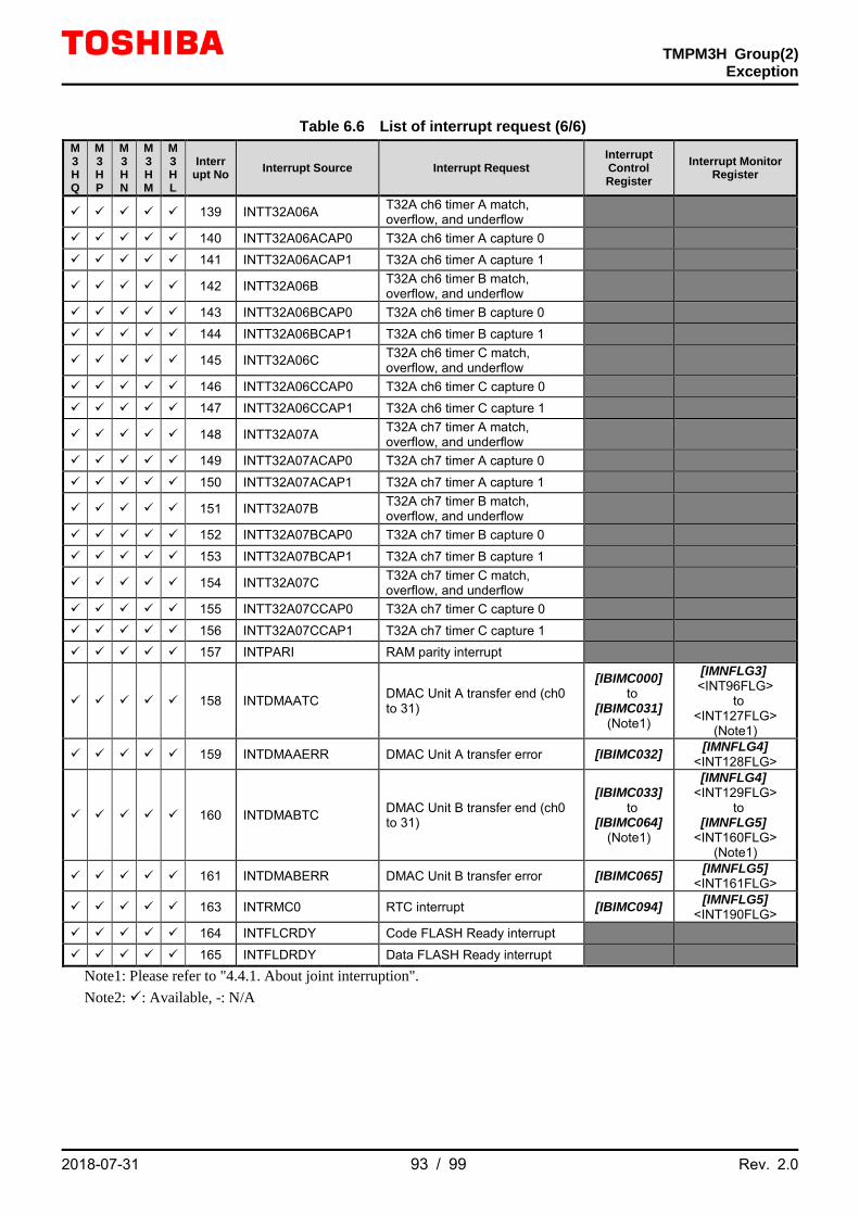
TMPM3H Group(2)
Exception
2018-07-31 93 / 99 Rev. 2.0
Table 6.6 List of interrupt request (6/6)
M 3 H Q
M 3 H P
M 3 H N
M 3 H M
M 3 H L
Interrupt No Interrupt Source Interrupt Request
Interrupt Control Register
Interrupt Monitor Register
139 INTT32A06A T32A ch6 timer A match, overflow, and underflow
140 INTT32A06ACAP0 T32A ch6 timer A capture 0 141 INTT32A06ACAP1 T32A ch6 timer A capture 1
142 INTT32A06B T32A ch6 timer B match, overflow, and underflow
143 INTT32A06BCAP0 T32A ch6 timer B capture 0 144 INTT32A06BCAP1 T32A ch6 timer B capture 1
145 INTT32A06C T32A ch6 timer C match, overflow, and underflow
146 INTT32A06CCAP0 T32A ch6 timer C capture 0 147 INTT32A06CCAP1 T32A ch6 timer C capture 1
148 INTT32A07A T32A ch7 timer A match, overflow, and underflow
149 INTT32A07ACAP0 T32A ch7 timer A capture 0 150 INTT32A07ACAP1 T32A ch7 timer A capture 1
151 INTT32A07B T32A ch7 timer B match, overflow, and underflow
152 INTT32A07BCAP0 T32A ch7 timer B capture 0 153 INTT32A07BCAP1 T32A ch7 timer B capture 1
154 INTT32A07C T32A ch7 timer C match, overflow, and underflow
155 INTT32A07CCAP0 T32A ch7 timer C capture 0 156 INTT32A07CCAP1 T32A ch7 timer C capture 1 157 INTPARI RAM parity interrupt
158 INTDMAATC DMAC Unit A transfer end (ch0 to 31)
[IBIMC000] to
[IBIMC031] (Note1)
[IMNFLG3] <INT96FLG>
to <INT127FLG>
(Note1)
159 INTDMAAERR DMAC Unit A transfer error [IBIMC032] [IMNFLG4] <INT128FLG>
160 INTDMABTC DMAC Unit B transfer end (ch0 to 31)
[IBIMC033] to
[IBIMC064] (Note1)
[IMNFLG4] <INT129FLG>
to [IMNFLG5]
<INT160FLG> (Note1)
161 INTDMABERR DMAC Unit B transfer error [IBIMC065] [IMNFLG5] <INT161FLG>
163 INTRMC0 RTC interrupt [IBIMC094] [IMNFLG5] <INT190FLG>
164 INTFLCRDY Code FLASH Ready interrupt 165 INTFLDRDY Data FLASH Ready interrupt
Note1: Please refer to "4.4.1. About joint interruption". Note2: : Available, -: N/A

TMPM3H Group(2)
Exception
2018-07-31 94 / 99 Rev. 2.0
Table 6.7 Interrupt Number 158 (1/2)
M 3 H Q
M 3 H P
M 3 H N
M 3 H M
M 3 H L
Interrupt Source
INTDMAATC (DMAC Unit
A)
Interrupt request Interrupt Control Register
Interrupt Monitor Register
ch0 TSPI ch0 Receive DMA request [IBIMC000] [IMNFLG3]<INT96FLG>
ch1 TSPI ch0 Transmit DMA request [IBIMC001] [IMNFLG3]<INT97FLG>
- ch2 TSPI ch1 Receive DMA request [IBIMC002] [IMNFLG3]<INT98FLG>
- ch3 TSPI ch1 Transmit DMA request [IBIMC003] [IMNFLG3]<INT99FLG>
ch4 I2C ch0 Receiving DMA request [IBIMC004] [IMNFLG3]<INT100FLG>
ch5 I2C ch0 Transmitting DMA request [IBIMC005] [IMNFLG3]<INT101FLG>
ch6 UART ch0 Reception DMA request [IBIMC006] [IMNFLG3]<INT102FLG>
ch7 UART ch0 Transmission DMA request [IBIMC007] [IMNFLG3]<INT103FLG>
ch8 UART ch1 Reception DMA request [IBIMC008] [IMNFLG3]<INT104FLG>
ch9 UART ch1 Transmission DMA request [IBIMC009] [IMNFLG3]<INT105FLG>
ch10 UART ch2 Reception DMA request [IBIMC010] [IMNFLG3]<INT106FLG>
ch11 UART ch2 Transmission DMA request [IBIMC011] [IMNFLG3]<INT107FLG>
ch12 UART ch3 Reception DMA request [IBIMC012] [IMNFLG3]<INT108FLG>
ch13 UART ch3 Transmission DMA request [IBIMC013] [IMNFLG3]<INT109FLG>
ch14 A-PMD ch0 PWM interrupt [IBIMC014] [IMNFLG3]<INT110FLG>
ch15
T32A ch0 DMA request at match A1 register
[IBIMC015] [IMNFLG3]<INT111FLG> T32A ch0 DMA request at match C1 register
T32A ch1 DMA request at match A1 register
T32A ch1 DMA request at match C1 register
ch16
T32A ch2 DMA request at match A1 register
[IBIMC016] [IMNFLG3]<INT112FLG> T32A ch2 DMA request at match C1 register
T32A ch3 DMA request at match A1 register
T32A ch3 DMA request at match C1 register
ch17 T32A ch0 DMA request at match B1 register
[IBIMC017] [IMNFLG3]<INT113FLG> T32A ch1 DMA request at match B1 register
ch18 T32A ch2 DMA request at match B1 register
[IBIMC018] [IMNFLG3]<INT114FLG> T32A ch3 DMA request at match B1 register
ch19
T32A ch0 DMA request at capture A0 register
[IBIMC019] [IMNFLG3]<INT115FLG>
T32A ch0 DMA request at capture A1 register
T32A ch1 DMA request at capture A0 register
T32A ch1 DMA request at capture A1 register
T32A ch0 DMA request at capture C0 register
T32A ch0 DMA request at capture C1 register
T32A ch1 DMA request at capture C0 register
T32A ch1 DMA request at capture C1 register
Note: : Available, -: N/A
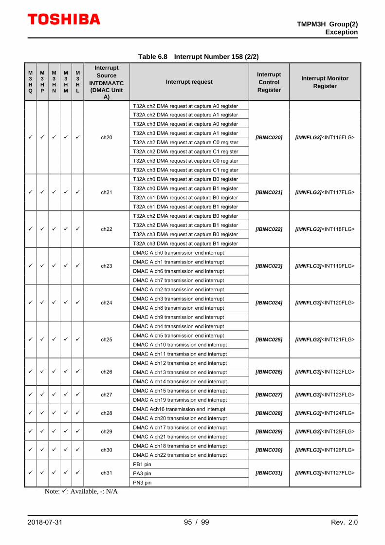
TMPM3H Group(2)
Exception
2018-07-31 95 / 99 Rev. 2.0
Table 6.8 Interrupt Number 158 (2/2)
M 3 H Q
M 3 H P
M 3 H N
M 3 H M
M 3 H L
Interrupt Source
INTDMAATC (DMAC Unit
A)
Interrupt request Interrupt Control Register
Interrupt Monitor Register
ch20
T32A ch2 DMA request at capture A0 register
[IBIMC020] [IMNFLG3]<INT116FLG>
T32A ch2 DMA request at capture A1 register
T32A ch3 DMA request at capture A0 register
T32A ch3 DMA request at capture A1 register
T32A ch2 DMA request at capture C0 register
T32A ch2 DMA request at capture C1 register
T32A ch3 DMA request at capture C0 register
T32A ch3 DMA request at capture C1 register
ch21
T32A ch0 DMA request at capture B0 register
[IBIMC021] [IMNFLG3]<INT117FLG> T32A ch0 DMA request at capture B1 register
T32A ch1 DMA request at capture B0 register
T32A ch1 DMA request at capture B1 register
ch22
T32A ch2 DMA request at capture B0 register
[IBIMC022] [IMNFLG3]<INT118FLG> T32A ch2 DMA request at capture B1 register
T32A ch3 DMA request at capture B0 register
T32A ch3 DMA request at capture B1 register
ch23
DMAC A ch0 transmission end interrupt
[IBIMC023] [IMNFLG3]<INT119FLG> DMAC A ch1 transmission end interrupt
DMAC A ch6 transmission end interrupt
DMAC A ch7 transmission end interrupt
ch24
DMAC A ch2 transmission end interrupt
[IBIMC024] [IMNFLG3]<INT120FLG> DMAC A ch3 transmission end interrupt
DMAC A ch8 transmission end interrupt
DMAC A ch9 transmission end interrupt
ch25
DMAC A ch4 transmission end interrupt
[IBIMC025] [IMNFLG3]<INT121FLG> DMAC A ch5 transmission end interrupt
DMAC A ch10 transmission end interrupt
DMAC A ch11 transmission end interrupt
ch26 DMAC A ch12 transmission end interrupt
[IBIMC026] [IMNFLG3]<INT122FLG> DMAC A ch13 transmission end interrupt
DMAC A ch14 transmission end interrupt
ch27 DMAC A ch15 transmission end interrupt
[IBIMC027] [IMNFLG3]<INT123FLG> DMAC A ch19 transmission end interrupt
ch28 DMAC Ach16 transmission end interrupt
[IBIMC028] [IMNFLG3]<INT124FLG> DMAC A ch20 transmission end interrupt
ch29 DMAC A ch17 transmission end interrupt
[IBIMC029] [IMNFLG3]<INT125FLG> DMAC A ch21 transmission end interrupt
ch30 DMAC A ch18 transmission end interrupt
[IBIMC030] [IMNFLG3]<INT126FLG> DMAC A ch22 transmission end interrupt
ch31 PB1 pin
[IBIMC031] [IMNFLG3]<INT127FLG> PA3 pin
PN3 pin
Note: : Available, -: N/A

TMPM3H Group(2)
Exception
2018-07-31 96 / 99 Rev. 2.0
Table 6.9 Interrupt Number 160 (1/2)
M 3 H Q
M 3 H P
M 3 H N
M3HM
M 3 H L
Interrupt Source
INTDMABTC (DMAC Unit B)
Interrupt request Interrupt Control Register
Interrupt Monitor Register
- ch0
TSPI ch2 Receive DMA request [IBIMC033] [IMNFLG4]<INT129FLG>
- - - I2C ch3 Receiving DMA request
ch1
TSPI ch2 Transmit DMA request [IBIMC034] [IMNFLG4]<INT130FLG>
- - - I2C ch3 Transmitting DMA request
- ch2 TSPI ch3 Receive DMA request [IBIMC035] [IMNFLG4]<INT131FLG>
- ch3 TSPI ch3 Transmit DMA request [IBIMC036] [IMNFLG4]<INT132FLG>
- ch4 TSPI ch4 Receive DMA request [IBIMC037] [IMNFLG4]<INT133FLG>
- ch5 TSPI ch4 Transmit DMA request [IBIMC038] [IMNFLG4]<INT134FLG>
- ch6 I2C ch1 Receiving DMA request [IBIMC039] [IMNFLG4]<INT135FLG>
- ch7 I2C ch1 Transmitting DMA request [IBIMC040] [IMNFLG4]<INT136FLG>
ch8 I2C ch2 Receiving DMA request [IBIMC041] [IMNFLG4]<INT137FLG>
ch9 I2C ch2 Transmitting DMA request [IBIMC042] [IMNFLG4]<INT138FLG>
ch10 UART ch4 Reception DMA request [IBIMC043] [IMNFLG4]<INT139FLG>
ch11 UART ch4 Transmission DMA request [IBIMC044] [IMNFLG4]<INT140FLG>
ch12 UART ch5 Reception DMA request [IBIMC045] [IMNFLG4]<INT141FLG>
ch13 UART ch5 Transmission DMA request [IBIMC046] [IMNFLG4]<INT142FLG>
ch14
ADC Unit A General-purpose trigger DMA request
[IBIMC047] [IMNFLG4]<INT143FLG> ADC Unit A Single conversion DMA request
ADC Unit A Continuous conversion DMA request
ch15
T32A ch4 DMA request at match A1 register
[IBIMC048] [IMNFLG4]<INT144FLG> T32A ch4 DMA request at match C1 register
T32A ch5 DMA request at match A1 register
T32A ch5 DMA request at match C1 register
ch16
T32A ch6 DMA request at match A1 register
[IBIMC049] [IMNFLG4]<INT145FLG> T32A ch6 DMA request at match C1 register
T32A ch7 DMA request at match A1 register
T32A ch7 DMA request at match A1 register
ch17 T32A ch4 DMA request at match B1 register
[IBIMC050] [IMNFLG4]<INT146FLG> T32A ch5 DMA request at match B1 register
ch18 T32A ch6 DMA request at match B1 register
[IBIMC051] [IMNFLG4]<INT147FLG> T32A ch7 DMA request at match B1 register
ch19
T32A ch4 DMA request at capture A0 register
[IBIMC052] [IMNFLG4]<INT148FLG>
T32A ch4 DMA request at capture A1 register
T32A ch5 DMA request at capture A0 register
T32A ch5 DMA request at capture A1 register
T32A ch4 DMA request at capture C0 register
T32A ch4 DMA request at capture C1 register
T32A ch5 DMA request at capture C0 register
T32A ch5 DMA request at capture C1 register
Note: : Available, -: N/A
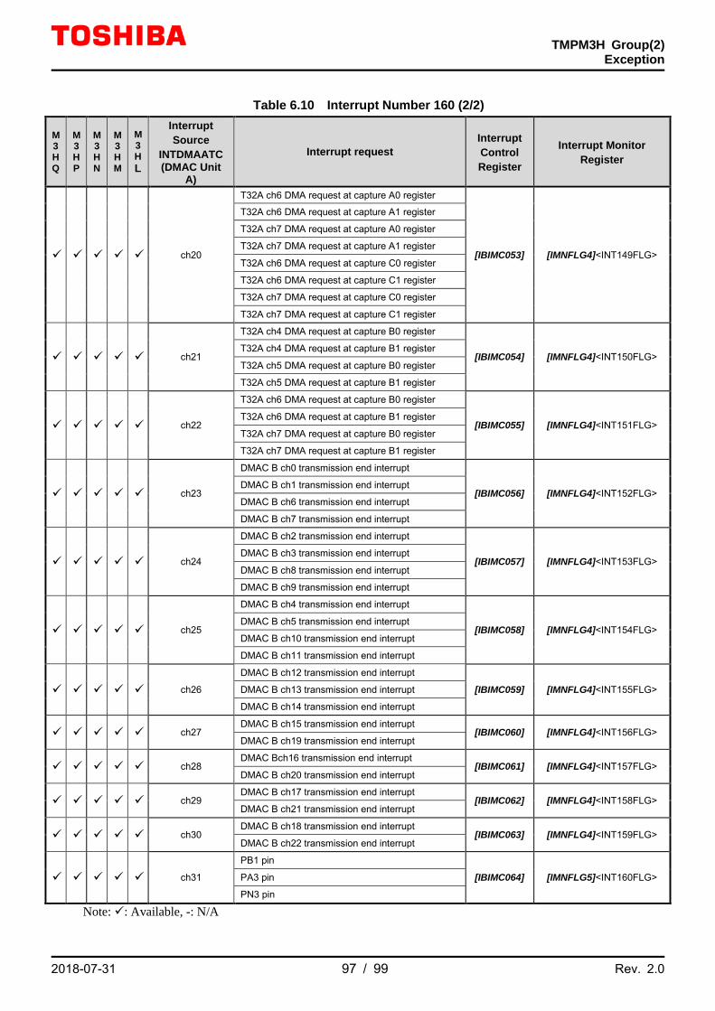
TMPM3H Group(2)
Exception
2018-07-31 97 / 99 Rev. 2.0
Table 6.10 Interrupt Number 160 (2/2)
M 3 H Q
M 3 H P
M 3 H N
M3HM
M 3 H L
Interrupt Source
INTDMAATC (DMAC Unit
A)
Interrupt request Interrupt Control Register
Interrupt Monitor Register
ch20
T32A ch6 DMA request at capture A0 register
[IBIMC053] [IMNFLG4]<INT149FLG>
T32A ch6 DMA request at capture A1 register
T32A ch7 DMA request at capture A0 register
T32A ch7 DMA request at capture A1 register
T32A ch6 DMA request at capture C0 register
T32A ch6 DMA request at capture C1 register
T32A ch7 DMA request at capture C0 register
T32A ch7 DMA request at capture C1 register
ch21
T32A ch4 DMA request at capture B0 register
[IBIMC054] [IMNFLG4]<INT150FLG> T32A ch4 DMA request at capture B1 register
T32A ch5 DMA request at capture B0 register
T32A ch5 DMA request at capture B1 register
ch22
T32A ch6 DMA request at capture B0 register
[IBIMC055] [IMNFLG4]<INT151FLG> T32A ch6 DMA request at capture B1 register
T32A ch7 DMA request at capture B0 register
T32A ch7 DMA request at capture B1 register
ch23
DMAC B ch0 transmission end interrupt
[IBIMC056] [IMNFLG4]<INT152FLG> DMAC B ch1 transmission end interrupt
DMAC B ch6 transmission end interrupt
DMAC B ch7 transmission end interrupt
ch24
DMAC B ch2 transmission end interrupt
[IBIMC057] [IMNFLG4]<INT153FLG> DMAC B ch3 transmission end interrupt
DMAC B ch8 transmission end interrupt
DMAC B ch9 transmission end interrupt
ch25
DMAC B ch4 transmission end interrupt
[IBIMC058] [IMNFLG4]<INT154FLG> DMAC B ch5 transmission end interrupt
DMAC B ch10 transmission end interrupt
DMAC B ch11 transmission end interrupt
ch26
DMAC B ch12 transmission end interrupt
[IBIMC059] [IMNFLG4]<INT155FLG> DMAC B ch13 transmission end interrupt
DMAC B ch14 transmission end interrupt
ch27 DMAC B ch15 transmission end interrupt
[IBIMC060] [IMNFLG4]<INT156FLG> DMAC B ch19 transmission end interrupt
ch28 DMAC Bch16 transmission end interrupt
[IBIMC061] [IMNFLG4]<INT157FLG> DMAC B ch20 transmission end interrupt
ch29 DMAC B ch17 transmission end interrupt
[IBIMC062] [IMNFLG4]<INT158FLG> DMAC B ch21 transmission end interrupt
ch30 DMAC B ch18 transmission end interrupt
[IBIMC063] [IMNFLG4]<INT159FLG> DMAC B ch22 transmission end interrupt
ch31
PB1 pin
[IBIMC064] [IMNFLG5]<INT160FLG> PA3 pin
PN3 pin
Note: : Available, -: N/A
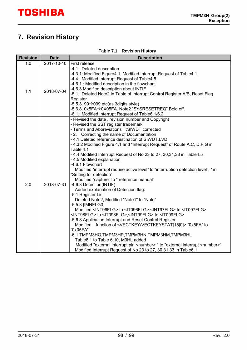
TMPM3H Group(2)
Exception
2018-07-31 98 / 99 Rev. 2.0
7. Revision History
Table 7.1 Revision History Revision Date Description
1.0 2017-10-10 First release
1.1 2018-07-04
-4.1.: Deleted description. -4.3.1: Modified Figure4.1, Modified Interrupt Request of Table4.1. -4.4.: Modified Interrupt Request of Table4.5. -4.6.1.: Modified description in the flowchart. -4.6.3.Modified description about INTIF -5.1.: Deleted Note2 in Table of Interrupt Control Register A/B, Reset Flag Register -5.5.3. 99099 etc(as 3digits style) -5.6.8. 0x5FA0X05FA. Note2 “SYSRESETREQ” Bold off. -6.1.: Modified Interrupt Request of Table6.1/6.2.
2.0 2018-07-31
- Revised the date , revision number and Copyright - Revised the SST register trademark - Terms and Abbreviations :SIWDT corrected - 2. Correcting the name of Documentation - 4.1 Deleted reference destination of SIWDT,LVD - 4.3.2 Modified Figure 4.1 and “Interrupt Request” of Route A,C, D,F,G in Table 4.1 - 4.4 Modified Interrupt Request of No 23 to 27, 30,31,33 in Table4.5 - 4.5 Modified explanation -4.6.1 Flowchart Modified “interrupt require active level” to “interruption detection level”, “ in “Setting for detection”. Modified “capture” to “ reference manual” -4.6.3 Detection(INTIF) Added explanation of Detection flag. -5.1 Register List Deleted Note2, Modified "Note1" to "Note" -5.5.3 [IMNFLG3] Modified <INT96FLG> to <IT096FLG>.<INT97FLG> to <IT097FLG>, <INT98FLG> to <IT098FLG>,<INT99FLG> to <IT099FLG> -5.6.8 Application Interrupt and Reset Control Register Modified function of <VECTKEY/VECTKEYSTAT[15]0]> “0x5FA” to “0x05FA” -6.1 TMPM3HQ,TMPM3HP,TMPM3HN,TMPM3HM,TMPM3HL Table6.1 to Table 6.10, M3HL added
Modified "external interrupt pin <number> " to "external interrupt <number>". Modified Interrupt Request of No 23 to 27, 30,31,33 in Table6.1

TMPM3H Group(2)
Exception
2018-07-31 99 / 99 Rev. 2.0
RESTRICTIONS ON PRODUCT USE Toshiba Corporation and its subsidiaries and affiliates are collectively referred to as “TOSHIBA”. Hardware, software and systems described in this document are collectively referred to as “Product”.
• TOSHIBA reserves the right to make changes to the information in this document and related Product without notice.
• This document and any information herein may not be reproduced without prior written permission from TOSHIBA. Even with TOSHIBA's written permission, reproduction is permissible only if reproduction is without alteration/omission.
• Though TOSHIBA works continually to improve Product's quality and reliability, Product can malfunction or fail. Customers are responsible for complying with safety standards and for providing adequate designs and safeguards for their hardware, software and systems which minimize risk and avoid situations in which a malfunction or failure of Product could cause loss of human life, bodily injury or damage to property, including data loss or corruption. Before customers use the Product, create designs including the Product, or incorporate the Product into their own applications, customers must also refer to and comply with (a) the latest versions of all relevant TOSHIBA information, including without limitation, this document, the specifications, the data sheets and application notes for Product and the precautions and conditions set forth in the "TOSHIBA Semiconductor Reliability Handbook" and (b) the instructions for the application with which the Product will be used with or for. Customers are solely responsible for all aspects of their own product design or applications, including but not limited to (a) determining the appropriateness of the use of this Product in such design or applications; (b) evaluating and determining the applicability of any information contained in this document, or in charts, diagrams, programs, algorithms, sample application circuits, or any other referenced documents; and (c) validating all operating parameters for such designs and applications. TOSHIBA ASSUMES NO LIABILITY FOR CUSTOMERS' PRODUCT DESIGN OR APPLICATIONS.
• PRODUCT IS NEITHER INTENDED NOR WARRANTED FOR USE IN EQUIPMENTS OR SYSTEMS THAT REQUIRE EXTRAORDINARILY HIGH LEVELS OF QUALITY AND/OR RELIABILITY, AND/OR A MALFUNCTION OR FAILURE OF WHICH MAY CAUSE LOSS OF HUMAN LIFE, BODILY INJURY, SERIOUS PROPERTY DAMAGE AND/OR SERIOUS PUBLIC IMPACT ("UNINTENDED USE"). Except for specific applications as expressly stated in this document, Unintended Use includes, without limitation, equipment used in nuclear facilities, equipment used in the aerospace industry, medical equipment, equipment used for automobiles, trains, ships and other transportation, traffic signaling equipment, equipment used to control combustions or explosions, safety devices, elevators and escalators, devices related to electric power, and equipment used in finance-related fields. IF YOU USE PRODUCT FOR UNINTENDED USE, TOSHIBA ASSUMES NO LIABILITY FOR PRODUCT. For details, please contact your TOSHIBA sales representative.
• Do not disassemble, analyze, reverse-engineer, alter, modify, translate or copy Product, whether in whole or in part.
• Product shall not be used for or incorporated into any products or systems whose manufacture, use, or sale is prohibited under any applicable laws or regulations.
• The information contained herein is presented only as guidance for Product use. No responsibility is assumed by TOSHIBA for any infringement of patents or any other intellectual property rights of third parties that may result from the use of Product. No license to any intellectual property right is granted by this document, whether express or implied, by estoppel or otherwise.
• ABSENT A WRITTEN SIGNED AGREEMENT, EXCEPT AS PROVIDED IN THE RELEVANT TERMS AND CONDITIONS OF SALE FOR PRODUCT, AND TO THE MAXIMUM EXTENT ALLOWABLE BY LAW, TOSHIBA (1) ASSUMES NO LIABILITY WHATSOEVER, INCLUDING WITHOUT LIMITATION, INDIRECT, CONSEQUENTIAL, SPECIAL, OR INCIDENTAL DAMAGES OR LOSS, INCLUDING WITHOUT LIMITATION, LOSS OF PROFITS, LOSS OF OPPORTUNITIES, BUSINESS INTERRUPTION AND LOSS OF DATA, AND (2) DISCLAIMS ANY AND ALL EXPRESS OR IMPLIED WARRANTIES AND CONDITIONS RELATED TO SALE, USE OF PRODUCT, OR INFORMATION, INCLUDING WARRANTIES OR CONDITIONS OF MERCHANTABILITY, FITNESS FOR A PARTICULAR PURPOSE, ACCURACY OF INFORMATION, OR NONINFRINGEMENT.
• Do not use or otherwise make available Product or related software or technology for any military purposes, including without limitation, for the design, development, use, stockpiling or manufacturing of nuclear, chemical, or biological weapons or missile technology products (mass destruction weapons). Product and related software and technology may be controlled under the applicable export laws and regulations including, without limitation, the Japanese Foreign Exchange and Foreign Trade Law and the U.S. Export Administration Regulations. Export and re-export of Product or related software or technology are strictly prohibited except in compliance with all applicable export laws and regulations.
• Please contact your TOSHIBA sales representative for details as to environmental matters such as the RoHS compatibility of Product. Please use Product in compliance with all applicable laws and regulations that regulate the inclusion or use of controlled substances, including without limitation, the EU RoHS Directive. TOSHIBA ASSUMES NO LIABILITY FOR DAMAGES OR LOSSES OCCURRING AS A RESULT OF NONCOMPLIANCE WITH APPLICABLE LAWS AND REGULATIONS.