Embed Size (px)
Citation preview

Based with permission on lectures by John Getty Laboratory Electronics II (PHSX262) Spring 2011 Lecture 9 Page 1
Today3/22/11 Lecture 9Analog Digital Conversion
• Sampled Data Acquisition Systems• Discrete Sampling and Nyquist• Digital to Analog Conversion• Analog to Digital Conversion
Homework• Study for Exam next week (in class 3/29/11)• Covers everything up through Lecture 8 and Lab 7
Reading• A/D converters (pages 612-641).
Lab• Do DAC pre-lab before lab meeting.
– Graded at start of lab!!!• Sequential logic lab book due 3/25 at 10am.

Based with permission on lectures by John GettyLaboratory Electronics II (PHSX262) Spring 2011 Lecture 9 Page 2
Analog Digital AnalogWhy convert from analog to digital
• Digital transmission and storage of analog signals • Compression, Reliability, Error Correction
• Digital signal processing• Powerful algorithm, adaptable, ease of implementation
Why convert from digital to analog• We live (see, hear, and feel) in an analog world• Replay stored, transmitted, or processed data
• Music, messages, movies• Relay information from computers to humans• Digital control of analog systems• Convert virtual worlds to reality

Based with permission on lectures by John GettyLaboratory Electronics II (PHSX262) Spring 2011 Lecture 9 Page 3
Key Elements of a Sampled Signal Processing System
*ref: Analog Devices; Application Note AN-282
*

Based with permission on lectures by John GettyLaboratory Electronics II (PHSX262) Spring 2011 Lecture 9 Page 4
Key Elements of a Sampled Data System
*ref: Analog Devices; Application Note AN-282
*Interface to sampled system:
• Precision buffer/gain amplifiers preserve the integrity of analog signal. Sometimes auto-scale input
• Anti-alias filter is a LPF, typically with steep roll-off to ensure there are no signal components >fsample/2 .
Converts the analog signal into a digital representation:
• Sample and Hold is analog circuitry that ensures the ADC sees a stable, unchanging signal for the time required to accurately perform the conversion. (allows for under-sampling – advanced topic in A/D)
• A/D can be any of a wide range of devices. More on this later.
A DSP is a microprocessor optimized for manipulating digitized analog signals:
• Perform operations such as digital filtering and FFTs.
• Often is also used for system control.
• Vector processors. Field programmable gate arrays (FPGA).
In many systems the signal is converted back into analog (sometimes after short or long term storage in memory):
• Latch holds the digital data until the D/A can finish the conversion. This also allows the DSP processor to move on to other tasks.
• The D/A reverses the process used on the input side of the system.
• Some systems are made to faithfully reproduce (CD players) or improve (noise cancelling headphones) on the original analog input.
The final part of the process includes additional conditioning in the analog domain.
• Some D/As can produce in-band glitches that must be removed at this stage.
• Analog filtering can be used to compensate for the discrete nature of the D/A, improving overall system fidelity.

Based with permission on lectures by John Getty Laboratory Electronics II (PHSX262) Spring 2011 Lecture 9 Page 5
Discrete Sampling of 10 Hz Signal at 5Hz
-1
-0.8
-0.6
-0.4
-0.2
0
0.2
0.4
0.6
0.8
1
0 50 100 150 200 250 300 350 400
Milliseconds
Sample interval = 200mS
Sample Rate = 5Hz
10Signalf Hz 5Samplef Hz

Based with permission on lectures by John Getty Laboratory Electronics II (PHSX262) Spring 2011 Lecture 9 Page 6
Discrete Sampling of 10Hz signal at 10Hz
-1
-0.8
-0.6
-0.4
-0.2
0
0.2
0.4
0.6
0.8
1
0 50 100 150 200 250 300 350 400
Milliseconds
Sample interval = 100mS
Sample Rate = 10Hz
10Signalf Hz 10Samplef Hz

Based with permission on lectures by John Getty Laboratory Electronics II (PHSX262) Spring 2011 Lecture 9 Page 7
Discrete Sampling at 20Hz
-1
-0.8
-0.6
-0.4
-0.2
0
0.2
0.4
0.6
0.8
1
0 50 100 150 200 250 300 350 400
MillisecondsSample interval = 50mS
Sample Rate = 20Hz
20Samplef Hz10Signalf Hz
Based with permission on lectures by John Getty Laboratory Electronics II (PHSX262) Spring 2011 Lecture 9 Page 8
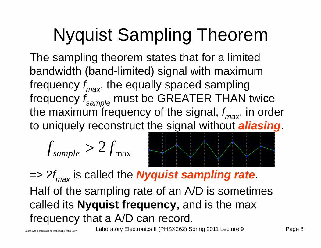
Nyquist Sampling TheoremThe sampling theorem states that for a limited bandwidth (band-limited) signal with maximum frequency fmax, the equally spaced sampling frequency fsample must be GREATER THAN twice the maximum frequency of the signal, fmax, in order to uniquely reconstruct the signal without aliasing.
=> 2fmax is called the Nyquist sampling rate. Half of the sampling rate of an A/D is sometimes called its Nyquist frequency, and is the max frequency that a A/D can record.
max2samplef f

Based with permission on lectures by John Getty Laboratory Electronics II (PHSX262) Spring 2011 Lecture 9 Page 9
Discrete Sampling at fs=2fmax
-1
-0.8
-0.6
-0.4
-0.2
0
0.2
0.4
0.6
0.8
1
0 50 100 150 200 250 300 350 400
Milliseconds
Sample interval = 50mS
Sample Rate = 20Hz10Ff Hz 20Sf Hz
max2sf ffs=2fmax is not sufficient,
Nyquist sampling requires

Based with permission on lectures by John Getty Laboratory Electronics II (PHSX262) Spring 2011 Lecture 9 Page 10
Aliasing
Sample_Rate_2.XLS
-1
-0.5
0
0.5
1
0 0.2 0.4 0.6 0.8 1SecondsOriginal Signal
22Sigf HzSample Freq.
20Sampf Hz
Sample Period
50SampT mS

Based with permission on lectures by John Getty Laboratory Electronics II (PHSX262) Spring 2011 Lecture 9 Page 11
Aliasing in the Frequency Domain
and L HF FSA ASf fff ff
The frequency of aliased signals is the difference between and sum of the sampling frequency fS and signal being sampled, fF . These aliased signals repeat around each integer multiple of the sampling frequency.
Sf
HzNyquist Frequency
LAf HAf8S
Fff
4S
Fff
2S
Fff
1.5F
Sf f
If you low pass filtered at fs , the you know only f<fs are real.

Based with permission on lectures by John GettyLaboratory Electronics II (PHSX262) Spring 2011 Lecture 9 Page 12
Digital to Analog Converter (DAC) TerminologyNumber of Bits:
A DAC with n bits provides 2n discrete output steps or counts. For example an 8 bit DAC has 256 possible output values.
Output Range:Difference between the maximum and minimum output values.
Resolution:Also known as the “step size”, represents the minimum change in output voltage. Typically equal to output range / (2n-1)
Dynamic Range:Output Range divided by Resolution or Noise Voltage.Would be (2n-1) if the noise was less than step size of DAC.

Based with permission on lectures by John GettyLaboratory Electronics II (PHSX262) Spring 2011 Lecture 9 Page 13
The 10 bits produce a total of 210 = 1024 steps.
The range is +12Vdc -(-12Vdc) = +24Vdc.
Therefore the resolution is 24Vdc/1023 = 0.02346V.
In-Class Exercise
Assume a 10 bit DAC is set up to output a voltage from -12Vdc to +12Vdc. Determine the resolution.
23.5mV/step!

Based with permission on lectures by John GettyLaboratory Electronics II (PHSX262) Spring 2011 Lecture 9 Page 14
One Approach to DAC:R-2R Ladder Circuit
1kohm 1kohm 1kohm
2kohm 2kohm 2kohm 2kohm
5V
Key = D Key = C Key = B Key = A
2kohm
Vout
1 2 3 452 2 2 2outA B C DV V
Vref
What is Vmax?Vmax=Vref*15/16=4.69V Vmin=0

Based with permission on lectures by John Getty Laboratory Electronics II (PHSX262) Spring 2011 Lecture 9 Page 15
10kohm 20kohm 40kohm 80kohm
1V
Key = D Key = C Key = B Key = A
Vout1
2
3
50kohm
4 3 2 1102 2 2 2A B C D V
2nd Approach to DAC: Scaled Summing Junction DAC
50 50 50 50180 40 20 10out
A k B k C k D kV Vk k k k
What is Range?Vmax=0, Vmin=-10V*15/16=-4.69V
Range=4.69V
This approach is the one we will implement in lab.

Based with permission on lectures by John GettyLaboratory Electronics II (PHSX262) Spring 2011 Lecture 9 Page 16
Analog to Digital Converter (ADC) TerminologyNumber of Bits:
An ADC with n bits divides the input range into 2n
discrete steps. For example, an 8 bit ADC can produce a total of 256 different output codes.
Full Scale Input RangeDifference between the minimum and maximum input voltage that can be measured.
Resolution:Quantization, also known as the “step size”, is the change in input voltage represented by each count at the output. Often referred to as LSB (least significant bit)
Dynamic Range:Input Range divided by resolution or noise. Typically equals 2n-1, if noise is less than LSB.

Based with permission on lectures by John GettyLaboratory Electronics II (PHSX262) Spring 2011 Lecture 9 Page 17
ADC Accuracy• QUANTIZATION ERROR Inherent accuracy (±1/2LSB, least significant bit)
• INTEGRAL NON-LINEARITY (INL) is a measure of the deviation of each individual code from a line drawn from zero scale or negative full scale (1⁄2 LSB below the first code transition) through positive full scale (1⁄2 LSB above the last code transition). The deviation of any given code from this straight line is measured from the center of that code value.
• DIFFERENTIAL NON-LINEARITY (DNL) is the measure of the maximum deviation from the ideal step size of 1 LSB. DNL is commonly measured at the rated clock frequency with a ramp input.
• MISSING CODES are output codes that are skipped or never appear at the ADC outputs. These codes cannot be reached by any input value.
• OFFSET ERROR is the difference between the ideal and actual LSB transition point.
• FULL SCALE ERROR is how far the last code transition is from the ideal 1.5 LSB below positive V_ref (V_ref is 2n times step size)
• GAIN ERROR is number of LSB “gained” from conversion from lowest to highest output. It is a measure of the deviation of the ADC from linear (gain = 1) conversion.
See figure 9.44 in H&H page 615

Based with permission on lectures by John GettyLaboratory Electronics II (PHSX262) Spring 2011 Lecture 9 Page 18
Ideal ADC: Quantization Error
-Quantization error is the inherent deviation of the output from a straight line.
-Note last transition is 1.5 LSB from Vref (used to measure full scale error)
Quantization Error
0
1
2
3
4
5
6
7
8
000 001 010 011 100 101 110 111
0.5 LSB
1.5 LSB
FULL SCALE ERRORQUANTIZATION
ERROR
Based with permission on lectures by John GettyLaboratory Electronics II (PHSX262) Spring 2011 Lecture 9 Page 19
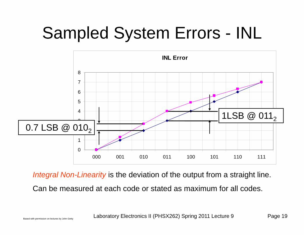
Sampled System Errors - INL
Integral Non-Linearity is the deviation of the output from a straight line.
Can be measured at each code or stated as maximum for all codes.
INL Error
0
1
2
3
4
5
6
7
8
000 001 010 011 100 101 110 111
1LSB @ 01120.7 LSB @ 0102

Based with permission on lectures by John GettyLaboratory Electronics II (PHSX262) Spring 2011 Lecture 9 Page 20
Sampled System Errors - DNL
Differential Non-Linearity is the maximum difference between the expected stepsize (1 LSB) and that steps actually produced by the DAC.
DNL Error
0
1
2
3
4
5
6
7
8
000 001 010 011 100 101 110 111
DNL=
1.0 LSB @ 0112
0 LSB @ 1002
(step is correct, but INL of 1002is 1.0LSB)

Based with permission on lectures by John GettyLaboratory Electronics II (PHSX262) Spring 2011 Lecture 9 Page 21
Sampled System Errors - Offset
Offset Error is measured at 0002.
Offset Error
0
1
2
3
4
5
6
7
8
9
000 001 010 011 100 101 110 111
1 LSB @ 0002
Based with permission on lectures by John GettyLaboratory Electronics II (PHSX262) Spring 2011 Lecture 9 Page 22
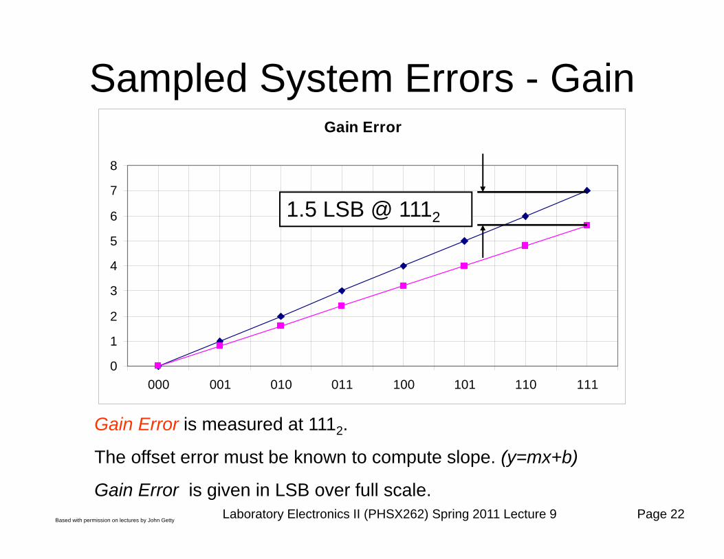
Sampled System Errors - Gain
Gain Error is measured at 1112.
The offset error must be known to compute slope. (y=mx+b)
Gain Error is given in LSB over full scale.
Gain Error
0
1
2
3
4
5
6
7
8
000 001 010 011 100 101 110 111
1.5 LSB @ 1112
Based with permission on lectures by John GettyLaboratory Electronics II (PHSX262) Spring 2011 Lecture 9 Page 23
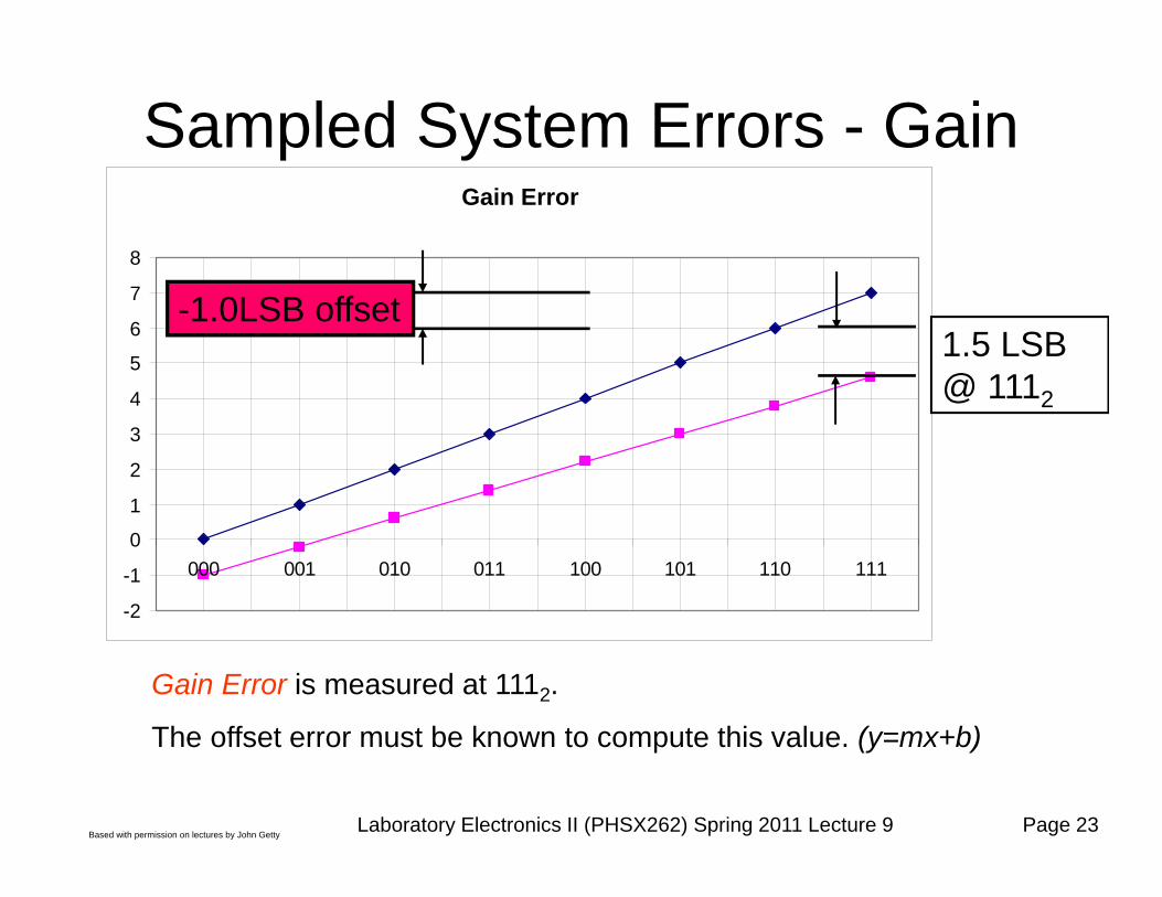
Sampled System Errors - Gain
Gain Error is measured at 1112.
The offset error must be known to compute this value. (y=mx+b)
Gain Error
-2
-1
0
1
2
3
4
5
6
7
8
000 001 010 011 100 101 110 111
1.5 LSB @ 1112
-1.0LSB offset

Based with permission on lectures by John GettyLaboratory Electronics II (PHSX262) Spring 2011 Lecture 9 Page 24
References1. Paul Horowitz and Winfield Hill (1989). “The Art of Electronics,” 2nd Ed., Cambridge2. Analog Devices, “Fundamentals of Sampled Data Systems”, accessed MAR 2008
http://www.analog.com/en/cat/0,2878,760,00.html3. “Efunda, Engineering Fundamentals” web site; accessed MAR 2008
http://www.efunda.com/designstandards/sensors/methods/DSP_nyquist.cfm4. National Semiconductor: accessed MAR 2008
http://www.national.com/appinfo/adc/files/definition_of_terms.pdf
![#] +e A ) - 日本弁護士連合会│Japan Federation of … ý Â Â Ë Â Â Ä Â Â Â Å 1 ý Â Â Ë Â Â Ä Â Â Â Å 5U ÊKS 1 ý Â Â Ë Â Â Ä Â Â Â Å1 ý Â](https://img.pdfslide.net/doc/110x75/5ce9840888c993c0208d8cce/-e-a-japan-federation-of-y-a-a-e-a-a-ae.jpg)


![Allen-Holberg - Cmos Analog Circuit Design 2ed Homework Solutions[1]](https://img.pdfslide.net/doc/110x75/553fe4244a7959a0098b4910/allen-holberg-cmos-analog-circuit-design-2ed-homework-solutions1.jpg)