Embed Size (px)
Citation preview
i i‘ "3 “O ‘ ' ‘ 2In this chapter, design and analysis of a wideband antenna using the fabricated
cylindrical dielectric resonator (DR) are discussed, with the support of simulated and
measured results. Starting with the fundamental broadside operation of a cylindrical
dielectric resonator antenna (DRA), a step-by-step development of the proposed
wideband antenna, using a low radiation Q-factor design is presented. Computer aided
high frequency structure simulator, Ansoft HFSSTM [1] is used for modeling and
simulating the antenna. Antenna characteristics such as the return loss, impedance,
radiation pattern, gain and radiation efficiency are measured with the help of HP 8510C
vector network analyser.
4.1 BROADSIDE MODE OPERATION OF A CYLINDRICAL DRA
The antenna study is starred with the cylindrical DR, DR-1 of dielectric
constant, std = 20.8, unloaded quality factor, Qt. I 6558 at 3.94 GI-I2, diameter, 2a
= 24 mm or 0.24 X0 and thickness, d = 7.3 mm or 0.073 X0, X0 being the free space
wave length corresponding to the fundamental mode frequency, f I 3.03 GI—Iz of
the DRA.
The antenna structure used for broadside radiation operation [2, 3] of a
cylindrical DR is shown in Figure 1. A 50 Q microstrip line, having a width = 3.3
mm and length I 50 mm fabricated on a 1.6 mm thick microwave substrate of
dielectric constant $1.5 =- 4 and size 115 mm x 115 mm, feeds the DRA. This
structure will operate on the fundamental broadside mode which is I-lEM11s (also99
456;" 1.18 \-§‘“ ‘ ‘,\'.-— t g ,l '2 5'1 ‘ii i.t,w*\‘* 33 QCI—I.AP1‘ER 4 EXPERIMEN ANALY “ 2pg W g _ g g g /f/‘S ‘ "C_c‘.\‘\"

">-—1:1__“-4-ljfiil~~~——T—__‘mlI-1.l1$-Iii %%%%%%%%%%%%% or ................... .t-W,.,._W-_a--
known as TMIIO [4]) for a cylindrical DR. This mode is very attractive in terms of
its lowest-Q factor compared to other modes of a cylindrical DR [5]. Impedance
matching between the feed and the DR can be easily achieved by adjusting the DR
position relative to the microstrip.
Cylindrical DR (std) l\4i¢r0StfipliI1@
d_$‘ /W K4Q1 II’ I I Z' .' 1,’' 20 -’5,- D, a 3 of 3 T 7 Q Ti?/‘ Y
Substrate (em)(with bottom ground plane)
Figure 1: Broadside radiation operation of the cylindrical DR
4.2 RESULTS
Measured and simulated return loss (|S11 |) of the DRA as a function of
frequency is shown in Figure 2, for an offset distance of 1 = 6 mm that
corresponds to the maximum impedance matching. The DRA resonates at 3.03
GHZ with a --10 dB bandwidth ranging from 2.92 to 3.144 GI-Iz or 7.38 °/o. This
high bandwidth is the result of the low radiation Q~factor of the excited mode.
The input impedance measured is 49—'j 4 Q. at 3.03 GHZ. Simulated resonance
occurs at 3.09 GHZ with a bandwidth of 4.28 %. The mismatch between the
measured and simulated results is attributed to the ideal modeling of antenna100

Clm_p!er 4
elements in I~Il"‘SS'““, whore the diclcc.t1"ics and conductors arc IISSLIITICLI to be
pcifcct.
In the literature [6], accurate closed form formulae for the frequencies of
the 1'c.\‘t>11:1n[ modes of :1 cylindrical] DR arc available. For the l"l'I"',1\I;|,~; mode, the
rcs<mz1nt f1'cqi.1c11cy is givcn by. - Z6.3240 u u1,1 = e——-—i<1.27+0.“@—+n.<>2i—] (4.1)' 27T('l,/<‘;‘[_d + 2L 3 20' \ Zd ]
whcrc c is the \'cl<__>ciq-' of light in Free space. The formula yields :1 frcqueiicy of
3.("'l5 CH2 which is in agrcL‘1n(%1"1t\\*ith the measured \-'z1luc.
O .=,, -.... _ . t-i 4 04 '\\ ______...---"""'_'__'i\ //\
s(dReturn Los B)E2_ .. .-I
__ ‘\\
-20- =Uit —— Measured i
—--—— Simu|ated(HFSS) U-30 : 1—~ -"" ‘:- ‘T "'"fi2.0 2.5 3.0 3.5 4.0Frequency (GHz)
l'igurc 2: 1\Icz1surcd rctum loss of the cyLindric:-11 DRA
101

E.\'pw'z'ment_u/ A in:/_\is'i.s‘
1\le:1su1'e.d fur-Ftcld radiation patterns in the m-'0 principal planes, natnely
X7, and YZ-planes of the antenna, at .’>.()3 Gllz are sh0\\-'11 in Figure 3. Patterns
are broadside, similrmr to that of a l1<'>ri2<..mtal magnetic dipole, with borcsighr cross
pc)l21risati011 levels of -22.61 dB and -16.34 dB in the XX and )'X- planes
respecti\'eh'. .\ls<> the horesight Fr<>11t-t<>-hack lobe rzltios are ~Z1.18 dB and -25
dB in the XX and YX-planes respectively and 21 gain of 5.71 dBi is 1ne;1su1'ed at the
1'es0nm1t f'reqt1e11c_\" of 3.03 GHZ.
90e .-1--_120 t \ 60\/ \\/’ -10 - \\// ""\ ‘150/ I \>:>"'“'\ \ soI .- / 9 - -..»’ I ; '. .° :- I\ . Iup 0.. C
//'I. X'./I./ '.Ii‘;-%.
-I>~ ullCD Q
'\
*L__..'\\ \, \0' \€_F____../'
'i_ Z //I" l } ) \.2 E . S. \ \ ;K-._ I ‘T’ \ §\0\_ 1 %@180t "' - ~":‘ T .. [LO
4'//5I9
*1.
. %.
/ "1-’?J\l- _.,
\
A ,' \_, “-"» /H / 330/
i -———-— YZ co-polarP; — — — YZ cross-polar |Q ———— —- XZ co-polar
no...--...~¢ CrosS-pO|a|'.. .__._. _2.7_O._ -__._t..
Pigtlre 3: Measured radiation pattern of the cylindrical DR.--\
In the f<>1lu\\'ing section, the broadside design shown above is tr21nsF<_>r1ncd
into 21 wideband, conical beam design.
102
_.~.- - _—.—_ _~_~_—>>_——_-: - - - - - -- -_=_»_»_—_— - -_ ,7 ~ —_ ;— — '- -; _ -.- . v -:.—._—.—.:_-.:;.
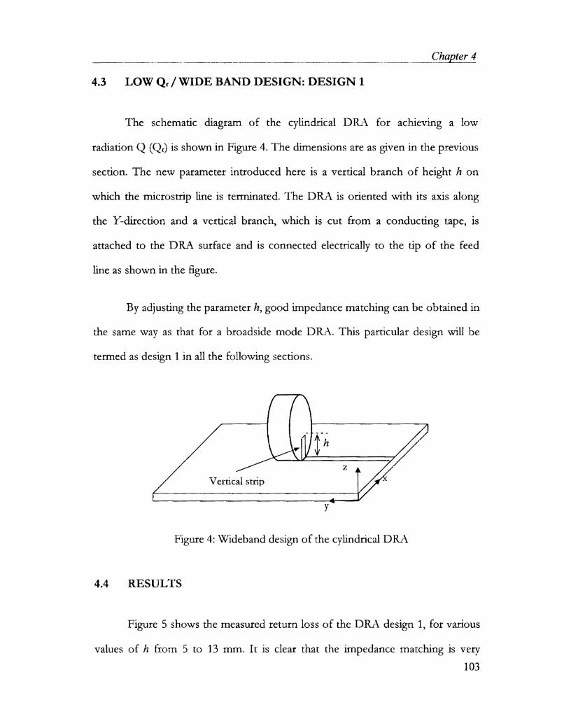
4.3 LOW Q, / WIDE BAND DESIGN: DESIGN 1
The schematic diagram of the cylindrical DRA for achieving a low
radiation Q is shown in Figure 4. The dimensions are as given in the previous
section. The new parameter introduced here is a vertical branch of height h on
which the microstrip line is terminated. The DRA is oriented with its axis along
the Y-direction and a vertical branch, which is cut from a conducting tape, is
attached to the DRA surface and is connected electrically to the tip of the feed
line as shown in the figure.
By adjusting the parameter h, good impedance matching can be obtained in
the same way as that for a broadside mode DRA. This particular design will be
termed as design 1 in all the following sections.
it2Vertical strip *S e s 4Y
Figure 4: Wideband design of the cylindrical DRA
4.4 RESULTS
Figure 5 shows the measured return loss of the DRA design 1, for various
values of h from 5 to 13 mm. It is clear that the impedance matching is very103

§1a2,et€m£a£qL4§9!y$i§....---,t . . . .. -..----v.---»--.¢--..-.-~.-».--.-.-.-A“-.~..--».
sensitive to the parameter h. For h = 9 mm, a maximum impedance bandwidth of
1120 MHZ or 35.94 % from 2.556 to 3.676 GHZ is observed. Bandwidth in
percentage is calculated with respect to the centre frequency of the -10 dB band,
which is 3.116 GHZ. A minimum return loss of -42 dB is obtained at 3.2 GI—Iz.
The wideband effect of design 1 is verified by simulation and the results
are shown in Figure 6. Simulated resonant frequency is 3.23 GI-I2 and bandwidth
is 1150 MHZ or 36.45 °/o (2.58 to 3.73 GI-lz) which are in good conformity with
the measured values.
0 a 7 =1
.-_._.\ ----- "“"'_}.‘:"'*"‘"'“':~‘r"'3-’-'-?\0%‘. ‘Ill /- -,,._9<y\‘.-7*‘ S %"--0 0" ’_ 0" 0*.>, ¥ ,:""'-' \.z°\r/'-J'\_.._/"%.a--‘“"-' '0' \.o /_. 1»"10 ' .0 \ .‘ ? P ’“"" ‘*7‘Q 7'“ \I */' ~__._ ’-* §_|l "ii
B
4% il 0I 01i
-20 -1
oss dReturn L
l
-30i —-—'—'— h=5mm
_40 n — "*'* —" 7 mm U——---~— 9 mm H———— —— ll mm 1.......... .. 13 mm ;\-50 + M I —~~e ~~1 | e fl2.0 2.5 3.0 3.5 4.0Frequency(GHz)
Figure 5: Measured return loss of the DRA for various strip heights (h)
104

.... IJ - ..... %%%%%%%% 2 iiiiiii flflflflflfl __.me ........... hezreril
Return Loss (dB)
Figure 6: Measured and simulated return loss of DRA, for h = 9 mm
mpedance (Q)
-1 1 — * | — -- r" ~ 1 I
0_ .\.\ é/1_ J10 % \\ //
\\‘\-20? \ /\-30 ~.~ \Z \A I
-40 J ——"i Measured I—- --- — HFSS V\
-50 1" ed * 1 — er 7‘ — *| |2.0 2.5 3.0 3.5 4.0Frequency (GHz)
200 e [150 _ -———-— real(Z) Measured........... IQ rea|(Z) I
\ _- -_ ---- -— imag(Z) Measured100 - :.' ....._.._.. in-|ag(X) HFSS’ \\/}'\
O 3l;.. _‘_-a'\.
\ O
\\\:.\: \..:-/»=' :
\.
..---<~='.:w___,_,.--" ,./. »¢‘ \ . %"%..1.o-""d’\\ /<./ \' 4/ \/T‘5O '1 \\_/>_ 12.0 2.5 3.0 3.5 4.0
Frequency (GHz)
Figure 7: Measured and simulated input impedance of DRA
for h = 9 mm

EX erimgiztql AnalMeasured and simulated input impedances of the DRA shown in Figure 7,
justify good and steady matching over the band. The radiation patterns of the
DRA are measured at 3.2 GHZ and are shown in Figure 8.
XZ-plane901 20 ' 60'\ i Q I’
150 M \ , so/
, ._ ~. ‘\210 \\ W/\ // 330' \ 7-0..-_. — __ __-‘. »_.—-1-— Co»poIar' ——— Cross-polar '240-“ 300
270
YZ-planeso120 ' so
, \/ ,150 so. \ ,
.-hi
Q
!§ - . n I210 V \*‘\\ / _/ t 330_ : '1. -\ 3 ,-
\
-—-—— Co-polar——— Cross-polar '24 ‘ 300
210
Figure 8: Measured 2-D radiation patterns of the DRA at 3._2 GI-I2,
for h I 9 mm
106

.As evident from the patterns, the XZ-plane pattern is symmetric and
conical in nature with a null of -24.71 dB occurring at the boresight or zenith (6
= 90°) and the maximum radiation at £9 = 145°. The cross-polarisation is -12.42
dB in the direction of maximum radiation and -4.92 dB in the boresight. This
high cross-polarisation in the boresight is due to the vertical strip, that may radiate
as a monopole antenna in the siinilar way as for a probe coupled DRA. On the
other hand, the YZ-plane pattern shows an asymmetry with a boresight null of
--10.12 dB and the maximum radiation at 150°. The asymmetry is due to the
effect of the coaxial cable and the connector, attached to the feed end of the
DRA. The cross-polar level is around -10 dB in the boresight as well as in the
peak radiation directions.
Stability of the radiation pattern over the impedance band is further
studied by comparing the patterns at different frequencies in the band. The co
polar patterns for three different frequencies viz. 2.6, 3.2 and 3.6 GHZ in the band
are shown in Figure 9. Cross-polar patterns are simply excluded for better
differentiation of the individual plots. It is clear that the symmetry and conical
nature of the XZ-plane patterns are preserved in the matching band, but the
pattern distortion in the YZ-plane becomes worse as moved from the lower end
to the higher end of the band. This is because, the disturbance caused by the cable
and the connector on the radiation increases with the frequency.
Simulated 3-D gain patterns are shown in Figure 10, which clearly show
the pattern distortion or squint in the band. Measured gain is 2.98 dBi at the
107

Exp?rim¢!2!@lrA ' " ' " ' mg‘resonant frequency of 3.2 GHZ, while the peak value in the band is 4.34 dBi
measured at 3.48 GI-lz.
XZ-plane90120 60‘u.
1". ‘.'.' -. '......,‘0o>.I= Q-..Ry i .. -HE / M5 "- 0- I0'. 5 . O- \ 0150 _ \ :20 F “ ’ 30
/ 1 - _\ \ _ _ _ '\ . : . ;\ . , . .\ .180 » t ~@ . L. aaaaaa 0
210’ ‘ _ at 330, -——— 2.6GHz
* — —-— 3.2 GHz ‘~Qoaoccuuoo
'\I _.P;':~"-_'0
\
\ \\270
YZ-plane90120 ' so
_ .'O..O
—L
U1@
Q
‘. ..‘..:.
I.// '
d i.’\ I CI ~'/' \_
OJQ
. .\. 5 -, 1 I/ '\ E 5 .~. . 2 . 0- -- -. 5 .- - I
\_ O; I ,
N_Lc>
Q
‘I
\I. _
I“.
\ \
coco0
I
-——— 2.6 GHz— — — - 3.2 GHz24L) ICOQUOOCOO 3J5(3+{z 3c“)
v
270
Figure 9: Measured 2-D radiation patterns of the DRA at
different frequencies in the band, for Y1 = 9 mm
108

Chapter 4
dI(a1 l“lTOt8 I ).5. 2060;->003
2 . GGOOQ->000
-1 . BOQDQ-0-BBQ
—H». 8066:-0-O00
-7’. BQGQQ-0-BB8
-1. 0260:-0-001
Figure 10: Simulated 3-D gain patterns of the DRA
As obvious from Figure 5, the wideband performance depends only on the
parameter h. Also a change in the center frequency of the operating band requires
a change in the DR properties. Thus design 1, though simple and easy to
implement, lacks in some free and flexible means for tuning the operating band
over a considerable range.
Incorporation of metallic sections on the feed as tuning stubs has been
shown to be a potential means for tuning the impedance matching [7] of DRAs.
In the present context, instead of fabricating additional metallic elements on the
feed, a new approach is used to modify the design 1, wherein the vertical feed
position is displaced backward from the strip end in order to add a microstrip stub
of length L to the design. As will be shown, the combination of the feed height h
109

Ex @rimq21ialtAtr2qly§ti§ts ______________ ,~___m.s___._.,_,_t,__ ________________________________________________________ ind,
and stub length L effectively helps to tune the impedance matching as well as the
operating band.
4.5 MODIFIED DESIGN WITH A HORIZONTAL STUB: DESIGN 2
The design shown in Figure 4 is modified by displacing the DRA and the
vertical feed on the microstrip, thereby introducing a horizontal stub of length L
in the design as shown in Figure 11.
/ ’ 1’, ZI L I_ t t We to ;
Y
Figure 11: Modified wideband DRA design
4.6 RESULTS
Plots of the measured return loss of the DRA for various strip heights (h)
and stub lengths (L) for a width same as that of the microstrip are shown in
Figures 12 (a), (c), (e) and As the figures show, for a given h, an optimum
value of L gives the maximum -10 dB bandwidth. As h is increased, the band is
shifted to a lower frequency range for a given L value. The bandwidth variations
with h and L are depicted in Figures 12 (b), (d), (f), and The parameter L thus
110
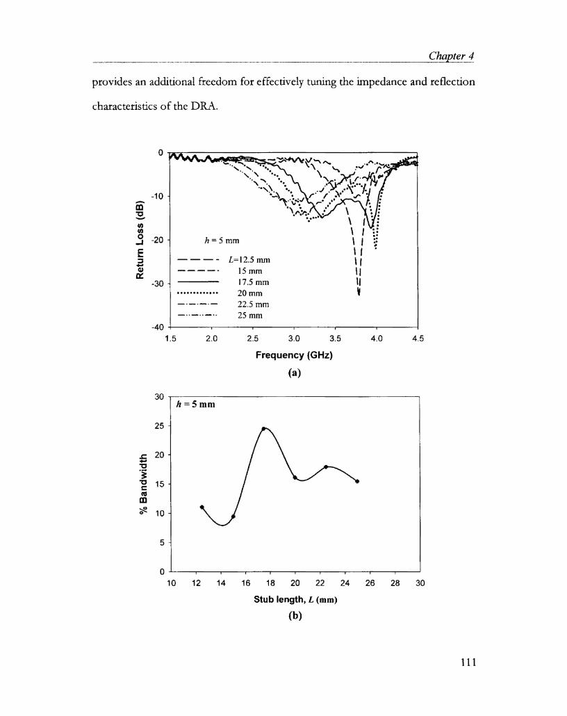
provides an additional freedom for effectively tuning the impedance and reflecnon
characteristics of the DRA.
Return Loss (dB)% Bandw dth
0
1141111514
.50» % "'-"‘..‘3~‘4'\/¥\I\-\,,_
/:./I /'
./' /' _
-10 I ~\,‘__<’_;_, r’__/'\fin. QI.\
-201 h=5mm
-30 1
——_IIZOOOQOOOOIOOIQ
1-3|-vim-iinnjauujov
L=l2.5 mm15 mml7.5 mm20 mm22.5 mm25 mm
.__. \\ R 4 /,\ H.‘ \ - "' *7"-gfi-§:.'fI'/-fl’.
Q‘ 53' \ €
.. u.A0.V~
all’2I --II-""11-__“MIII
-\%%1 Q OOOQ."...
-40 -L _.__.'.
1.5 2.0Frequency (GHz)
(m
I I‘ I W" I I I2.5 3.0 3.5 4.0 4.5
30 "V
25
2(I'*
15
101
5".
= 5 mm
0 “-2 I I f"'?’“iI I I* —I' ' I I1O 12 14 16 18 20 22 24 26 28 30
Stub length, L (mm)
W)

5'.§29Q€L”§Z".w?”e?Ql.A!?€{Zl%§§S e -“ V109 mm W.W.._
Return Loss (dB)% Bandw dth
-10
0
-20 _
-30 -+
-40 l
is0/9..
/.'-'.///1
.-1" /.~',//
0'...;"/£5" 2/ /- /
<"' (’ '2 /______...> .___, fa,
xx\
14'
I
0"‘: “:00”
h=7mm 0‘-1--— L=l5 mm
lT5mm20mm
---- -- 22.5 mm............ 25 mm
27.5 mm-50 1 e I“ ' "-1 ‘~ | e— |1.5 2.0
40
30
20
1 O
0 ‘T F "e f I * I‘ 1 e‘ I "'1 J14 16 1s 20 22 24 26 2a so
' /\.-\.\,. ./J-‘Ix\ \ ,_.':“ rd--’ _,.::\/". 0 -1’\ //‘ \
\
2.5 3.0 3.5Frequency (GHz)
(c)
4.0 4 5
_|-‘
“TlI
I
h=7mm
Stub length, L (mm)
(<1)

_- _ { - , _ Ch“ fer 4
Return Loss (dB)% Bandw'dth
0
-20
' .0 ,/:1‘WQ?\‘\ /'“ix '. 040- \\~Q?¢..»-~*<’”'
h=9mm
60- __"__
~40 q ~15 Z0
401
§xx»!
a&n:. ./f'/->( /
\\ \<._.L\ ./~ 3,. X\/ \ -.'-' />4.:///\\\ I’
j¢I'.p-v""""\q_* \n &i
L=225lnn125mm215mm30mm325mm35mm 1 I"25 30
Frequency (GHz)
(e)
30
20
I
\
10 J
OJ
h=9mm
20 24 ”'””'I" ' ,7! I 7"‘28 32 36 40Stub length, L (mm)
(T)

§1m¢rim@r1z{qlAnalyrs1'§ _ »-.¢v-»»--w-----—~—-—--~----w-~»--~_~n----- ------------- -- ..-~ w..-v-2-w.~-~-v.---.-.... ......_....,~--.»-\-.-~
0 A — 2 ~ 2--O Q I.‘-3.“;0.1%-is 1-. ..// all‘.
'§-/'/1/
..\ {\<\_\L\\
\\ ~~ _,..,-10 - \___'»hY~.»-20 - '_
Return Loss (dB)
_____, .--""<"“x
. -313"1
”\»
-30 - h = 11 mm-————- L=25 mm
_40_ ——— 27.5mm ¥-——— 30 mm---- -— 32.5 mm AI Q n - ¢ - o n u u | o00-50 '1’ I 1 _t,_ ,_1.4 1.6 1.8 2.0 2.2 2.4 2.6 2.8 3.0
Frequency (GHz)
(2)
30 —~ »h=l1 mm
25
20
% Bandw'dth
15-3
10*
5
O r (1 2|“ 2- I “er F 2'-*% ‘| "20 22 24 26 28 30 32 34 36 38 4O
Stub length, L (mm)
(h)
Figure 12 (a) - (h): Variation in return loss and bandwidth of the DRAwith h and L
114

.- — ——_——_ —_¢_—__—_—__-;—_~.—-w.-----;;;—_:_==--~»_»__-_=_=_—_~_-<—.-.».-- — — — ~ '—m_i—i—__—__-,1-__?;¢—_~-~ — — ~ ~ '—~__—;_—¢__—___—_1_-—~‘--~ — —— —— — '—_~___—_——_—:—_—__—— - ~ ~ 11' - — — ~ ~ ~— _—_—_¢;_— _——_——>.|-,---~-——-- - ;;_ —__ ——_——_—;_;_'__'~,_~~.--....- — —_— — —_—__— _—— ___ ___'_ha2.£§>"4
Summary of the reflection characteristics of the wideband DRA obtained
from Figure 12 is given below.
Table 1: Reflection characteristics of the DRA for optimum h and L
Strip Stub * —10dB Mid-band Bandwidth %height length = Frequency ifrequency MH Bandwidth
. 5 17.5 1 3.15 -4.03. L. i 3.59
(mm) i<L, mm), rang¢ <GHz> <@Hz> 1 ‘ Z’ . - ‘880 1 24.51
7 25 1 2.43 - 3.47J ._ . Li _ 2.95 I . - 11040 5 35.25. W . H1 9 27.5 2.01 - 2.85 2.43 840 1 34.572 11 30 I 1.89 — 2.43 2.16
, . ‘ . F540 25
From the measured results of Table 1, optimum values of h and L can be
expressed empirically as
7» 7»h av ° and L 1: 1° (4.2)3\/Q \/Qwhere X0 is the free space wavelength at the mid band frequency and std the
dielectric constant of the DRA. Here, the designs with h = 7 mm, L I 25 (design
2a) and h = 9 mm, L = 27.5 mm (design 2b) are chosen for further analysis since
these provide the broadest bandwidths in excess of 30 °/o. The other two designs
(h = 5 mm, L = 17.5 and h = 11 mm, L I 30) will be treated later. Figure 13
compares the measured and simulated return loss and input impedance of the
DRA for design 2a.115

E¥B€Ki"?§'1f¢{lA."ab’$llS I
Return Loss (dB)
.5
mpedance (Q
O
i
i
-L-5
-10i
-15 _
-20 '1‘!\.
-25 _
-30 1
_ -.~.._.:.______. —e__—:-_—;=;~ ~" -?>:—=:;—.-;:::;i ' --- ~ -- ---- ---.-.~-.-------.--~ ---- -w-~~»»»w»--1-—--9-»-»»»~w~mnn-—-----—~»»-~»~»--um- --------- ------u------ ----------- v----------\ / I// .\ /\ /\ /\ /
————- Measured-——— HFSS =I ' I I“ ' “if " I1.5 2.0 2.5 3.0 3.5 4.0 4.5
200 ~
Frequency (GHz)(3)
150 ~‘
I
100 q
50*
\
‘ I-so0 '.%.,__:.=f‘=g’=:_* ),ouP
-100 1. *—|
-—-——— real(Z) Measured ....... ..... .. rea|(Z) HFSS———— -——— 'mag(Z) Measured—---—----~ imag(Z) HFSS
. . . o I O QO. . .O. .... Q Q /I. 9 0. 1/‘JVT1 °. / J‘.0 Q o.00 0' ‘fin /ii‘ 00,,go ,[ \ % norM , \ ''\ 3:»-9% .
’ I I _‘ " I2.0 2.5 3.0 3.5 4.0Frequency(GHz)
(b)
Figure 13: Measured and simulated (21) return loss input impedance
of the DRA, for design 2a (h = 7 mm and L = 25 mm)
116

Simulated —1OdB bandwidth is from 2.4 to 3.41 GHZ (1010 MHZ) or 34.77
% at the centre frequency of 2.905 GHZ, which are in good agreement with the
measured results shown in Table 1 that gives a 2.43 to 3.47 GI-Iz or 35.25 % band.
XZ-planeso120 60
33Q _>I3 O1Q C/ \_\ W \| " i i -'|' \ -4 . . 4'» -6'» 8 8' 1 \ -+,.; _“_.\)/.\\J d3 __ 8O O
' ,;gg I-"g; -§\\1so . \ . -40):” 1 . l g 0
210 ' ' 330_ —-—— Co-polar
—-— Cross-polar '
270
YZ planeso120 so
1 _1Q.=_. - -I 2 \150 _ ‘ /""7, _20 *\ so
---; Co-polar. —-—-- Cross-polar240 300
270
Figure 14: Measured radiation patterns at 3.01 GHZ, for design 2a
117

EnwimentqiAI1¢1ly_@.*‘iL...._r_._.._--_---............._....-_..__.-_.-._........._......_______.. ................ ......_.-..._..._....
Two dimensional radiation patterns measured at 3.01 GHZ that
corresponds to the minimum measured return loss in Figure 13 (a) are shown in
Figure 14.
As observed from the radiation patterns, the conical nature is maintained
in both XZ and YZ-planes than that of the design discussed in the previous
section (design 1). The boresight nulls are of -36.67 dB and —24.56 dB in the XZ
and YZ-planes respectively. Cross-polar levels are of -6.31 dB and -12.73 dB at
the boresight respectively for the XZ and YZ-plane patterns. Peak radiation
occurs at 130° and 150° respectively in the XZ and YZ-planes, with the
corresponding cross-polarisations of -14.12 dB and -11.84 dB. Gain
measurements yielded 4.65 dBi at the resonant frequency of 3.01 GHZ and the
maximum gain in the band is 5.58 dBi at 3.4 GI—Iz.
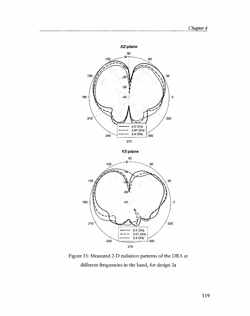
Figure 15 shows the measured co-polar patterns at the lower, mid and
upper ends of the matching band respectively at 2.5, 3.01 and 3.4 GI-I2. It is clear
that the symmetry and conical nature of the XZ-plane pattern is stable in the
matching band similar to the previous design. However, the YZ~plane pattern is
less distorted with the increase in frequency unlike that in design 1. This is further
confirmed by the 3-D radiation patterns of Figure 16.
I18
_ _ ___ . - _ — — — —_—; 1'. ; .—;~.—>>:.~.—.;-_—.-_~_ .-. -.
XZ-plane90
WC MP1" 4
1 20 60iJ. \\ O.9... 0..H’I’:/"
0..\\0.x
.0
1| ZIP8 ..I0...... ’
150 / _ _ ../:' i '. ~, IJ: ’ 1I: ;3g..!'_ __
-1WO
..¢000O
5 I
;, 4::::::i:\ \
{J \___ \ ..§ .-.\/-\ \-' \
\\
\-’- '
. ‘JglI
1\".\
l\)_LO
I I‘I, IIO
UO
4'"
\,.__QI
O0OJO
11
--— 2.5GHz——- 3.01GHz
240 _3'4 6"’ 300
270
YZ-plane90
120
.;1'-3:, [\.-.10-.-L» ..
60
09¢‘/ \ " -.¢.".*’.'-7?/ ~ -V \150 / ' ‘- l -2 I \. 30all _. I . \\ _/O \ -_ .. \..
\\ :7- - \\ .»' <. J, . ‘ D ./' ..QIQ Q. , I. _ H... -I_ , ll'OQ.O '-- ———- 2.5GHz
-——- 3.01GHz' -------- 3.4GHz
240
270
Figure 15: Measured 2-D radiati
differen
1-L0:O
ro_LO . 1.1.?!-f-'&°''0...)-' // .
P / ail.
- _‘.‘_?<-1;
OOO
'7'77.1\|-W"
(.0(.0O
f O
300
on patterns of the DRA at
t frequencies in the band, F dor esign Z21
_\ 30I. \
._\

Experimental Analysis
clO(O81 n1’ota‘l ).5. ae0B¢-Bea
1 2 . OQQQO-0-QQG
-1. Q@@¢O4'@QO'
—\-Iv. B0830-FQOBQl
-7. B8838-PBBB
-1 . @@BBQ+BB'1
PM
Figure 16: Simulated 3-D gain patterns of the DRA, for design 2a
For design 2b, the agreement between measured and simulated results is
shown in Figure 17. Simulated bandwidth is 817 MHZ or 32.42 °/o from 2.11 to
2.927 GHZ at the mid-band frequency of 2.52 GHZ, while that measured is 840
MHZ or 34.57 °/o from 2.01 to 2.85 GHZ.
120

—_mm%“%»
Return Loss(dB)
27
mpedance Q
.,.--....iiiiiiiii-15W /
‘ /-10 \\ /I-20 — \\ I -i Measured
1 ‘ — 1 “"2 I M‘ I * I ‘ ‘ _ I
0 “‘\2“ ...-\ /‘, \-5 ‘ \/~-—--J-'/2 \
, — — — HFSS \25 -1 | *'"| | —‘ | ‘ ‘ | —*-11.2 1.6 2.0 2.4 2.8 3 2 3 6
F requency(GHz)
(3)
200 W
\150 -2 i reaI(Z) Measured; . . . . - . » - ¢ . .IO |'ea|(Z) \———— -— imag(Z) Measured
100 7 —--—----- imag(Z) HFSS
50 - ........ .._. .......... ..: ........0".1O. »"'T2" ../' '\‘ ... ,.-=v'*"" r0- / _/ z\~R --5.-"7"".-I. \
\*4
\.‘
I )//J/' \"7"_“. 7-"?/ .-/-50 Y//_./'
|
1.8 2.0 2.2 2.4 2.6 2.8Frequency(GHz)
(b)
Figure 17: Measuxed and simulated (a) return loss (b) input impedance of
the DRA, for design .2b (h I 9 mm and L = 27.5 mm)
121

!s21§p¢rim@~wl <%!:wly~Yi~L.._ ~.--»- --»-we----~o-w--v-~-----------~-~w- --~v---»-.w--\-~»-~ --‘H.-..-- ...-...... ,.,,., ,., ..,.,.~.,.,.,....,,..._..,,,,...,,.-....,.,...-- - — ;..~:—---_—--_——_—
XZ-plane90120 : 60
/' \150 I ___ :20...?______ 30
i\__"
- '. 1'~ Ix-''. 1 \
-3»
... Q
\:~<_\\r
.- 5., \'-_ \180 3 -40 { W 0
I _ §,\.__ La,\ /I \ /'-' : _ / _ ,210 " * \" Va I V 330I5
——i-- Co-polar V240 ——-— Cross~poIar 00
120\
\
270
905 60‘/ "5‘ = 30
_s@C)
\
139' 'x\
\ I\ .Na:*- _/210 \' -V ‘s30'\
———— Co-polar--—— Cross-polar240 it _ 0
270
Figure 18: Measured radiation patterns at 2.43 GHZ, for
design 2b

_.- - %%%%%%%%%%%%%%%%%%%%%%%%%%%%%%%%%%%
Radiation patterns measured at 2.43 GI-lz, the centre frequency of theband
are shown in Figure 18. XZ and YZ plane patterns are more symmetrical and
conical shaped than those of the previous designs (design 1 and design 2a). The
nulls are at —-40 dB and -19.56 dB in the boresight for XZ and YZ-planes
respectively. Cross-polar levels are of -26.5 dB and -14-.93 dB respectively at the
boresight for XZ and YZ-plane patterns. Peak radiation occurs at 130° and 150°
respectively in the XZ and YZ-planes, with the respective cross-polarisations of
-14.73 dB and -21.47 dB. Measured mid-band gain is 4.39 dBi and the maximum
measured value in the band is 5.57 dBi at 2.36 GHz.
From the 2~D patterns measured for different frequencies, at 2.15, 2.43
and 2.8 GHZ shown in Figure 19, it is clear that the design 2b produces good
conical radiation patterns over the matching band. Simulated 3-D radiation
patterns shown in Figure 20 also confirm the pattern stability over the band.
Measured far-field transmission coefficients S21 in the direction of
maximum radiation of the DRAs so far studied are compared in Figure 21. It is
clear that peak |Sg1|corresponding to design 1 is lower than that of any other
designs in their respective bands, hence results in the lowest gain of all. The peak
gain of the broadside DRA is comparable to that of design 2. Table 2 compares
the various aspects of the wideband designs so far described.
Radiation patterns at other two combinations of h and L, i.e. h = 5 mm, L
= 17.5 and h = 11 mm, L = 30, shown in Table 1, were also measured. The
patterns measured at the centre frequencies of the corresponding bands i.e. 3.59
123

Exgerirrenfaléltqb/¢:i§rttor - tGHZ and 2.16 GHZ respectively, are shown in Figure 22. As observed, the conica
nature of the patterns is much deteriorated at the higher frequency (3.59 GHZ
Also these designs provide maximum gains around 4 dBi.
150 _2o ____ _
XZ-plane90120 60
\30*1." .| .' \'. ' 4'. \-30;
._(. ._ . || - .1 .180 .Wm. mW“40@@m
\.\. '-\
150
up-S
G)O
gpS:J:24g“‘
210
6 “;..:::
240
\
If
"'~?-=:
i 330
———-2.15GHzQ Q ¢ Q - -¢- '-—-- 2.8GHz | 300
\,__
YZ-plane90120 so11$‘ I _
I/ff. ..... ,_ _S,<m '.. _ _. I... \ ....o.::::..... .0 f-P ,- §\'.‘‘Q ‘Qt-I \-,. _I - _\‘.E " \ \0
;,'_. ,
\ '- _- ._o_..;.,,...._.3v,_3I.sz, . _..‘_.-.'.___..9'-f'\.-'1
-. I
.'..'.“. A
- ""'==.-:::'O)00O 0
_I ”.:.- 0 .1*-av" .0 .
\4w:\g‘ / ;v\/' '_ I -Q . Q-. , - . .\ . .- -t-a1 -.
—-— 2.15 GHZ' ---- -- 2.43GHz
240 .---. 2_3 GHZ 300
Figure 19: Measured 2-D radiation patterns of the DRA
at different frequencies in the band, for design 2b
1

Chapter 4
dB(Ga1nTota1)5. BBBBe+-BOO
2. OBOOO-PO09
‘ -1. $038+?
-H». B0388-I-Bi
-7. OQOBO4-BOB
-1. OBBDO4-B31
Figure 20: Simulated 3-D gain patterns of the DRA for design 2b
-25 0 1?,../ .\“»£€ J’: o'..§\ 000-30 _ I: /O .: 0...‘; ‘.0 1 . Q 0 Q Q00" \.. / .- ’ \
-35 _ ......°./l'..° ’,___// ' .\\
(dB)
\.
_:.
____4Ola§ ‘j X K i0 I I ‘x!-45 - /"\Vi\ /-I -i Broadside DRA
_ _ \- ........... .. Design 150 ---- —- Design 2a: —'-—--—-- Design 2b'55 1 I | | I I I1.5 2.0 2.5 3.0 3.5 4.0
21
\
\
j£7—“T'"/’f:.f:'I‘. j§ ‘J‘Q1?I “X
Frequency (GHz)
Figure 21: Comparison of the far-field | S31 | of the DRAs
125
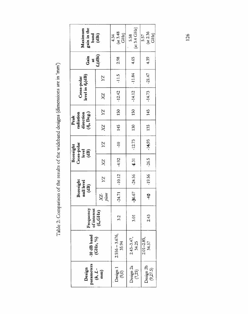
QJNUWW N“ noawwamos Om Em"Swag Om fig gggsg mgwmmm @8955 mg 5 “BBQUzi: MU9HN80HOHm lg aw U25 & m__O_fi___ODO< awvOm _a2flmHQ: h I AQmN_ A_\_vV Apvom Ii! _BBVNV_wo§mmr_OBU?wo_2__O<O_E5woammmg5:: _2a_“U09:BEMEO:&__w&O__3; UnaXN_ MAN XN KNkg“ MW MN %N XN %NO__omm|_vo_&___ zaiaca_O<O_ E suawv 95 ma: E =8UpuaQM“; W E5“figUfimwms H N28 I gayApe 3% jWM_N:_ |_o_B H is ‘B5 ac ZLmgL; gmQ: pgOINV_ gs £8 4‘U853 Np N$|Pk3_ weQQS §_€ lag Igfi:0 Go V IKPN|:_MKpaamwAg 9% OINVWW“;K Ggmvi N_O_|N_mw_ (cams Q0 fig _ N3‘R6 |B_g ‘MGM _:__£fia T5 IZHW‘ShhPgAg MUGOENV VEQ

---~...----o.-..---~--\»~w ---n_;;;;.'_<—_—.—_w-..---o-' ~ —— ~ -_=.._. ~>.- -— _ ——_—_-_v----~--'-—— — —
XZ-plane _ 9°120 ' so1"’_.-103 ~ .'
150 /L" * _2o -3';| "\- ‘ W180 “mu ; mmmlm ‘\407U '
M ‘if. l/ ' " "
L‘. .
(.0oQ
-'- -” \‘v;; '2 5 3210 _ \' "/' 330240 ‘ 300
—_::;‘i—»_-_-_-_-~\-~-— - ~ — --—-—- —
270 Coipglar'——— Cro Iar!.\cz1Qkuqe 90 L .______-mi¥tB2mnJ120 ’ e so
150 W /"_;'.-‘f-\ ‘ so
180 { -1 '/ HH1_4O'L‘ Mflu. 7;HH%. 0
\\ K./' I“; \ '" /'\ _. '- ' i210 V = . \i _’/ 330
LOC)
/5
240 ' 300270
00
Figure 22: M
90 XZ-plane120 ’ so1 _\150 / ‘ *fll ._ H \
--40
. I ,_ ,I'\ I I I .?{ ,_r~'210 ‘ / i aao4
65O
._ __ ; 1 u./—"-* O / "- ?\\1 I »»- '. W 1. L lxg 2( *3 *..=~;.- -.,-/ 5 »\__,_ \ _ Q X I /_ \~§;__,¢P 78O O
90 YZ-plane120 5 60.:10 -~ '
150 “A I : \ //!_*\.\ so" /">229 | ._1 ’ '.- 1/I ‘.3-O //180 N", J210 _. ‘ 330
240 300270
U9
a) — mm, L == 17.5 at 3.59 GI-Izeasurcd-radiation patterns for ( h '" 5
(b) h =11n:1m,L= 30 at 2.16 GHz
127
-------- -—---w- — ~ '~-_-_-,¢-5-_-.::_::~; .--_-\.- ,4-.\
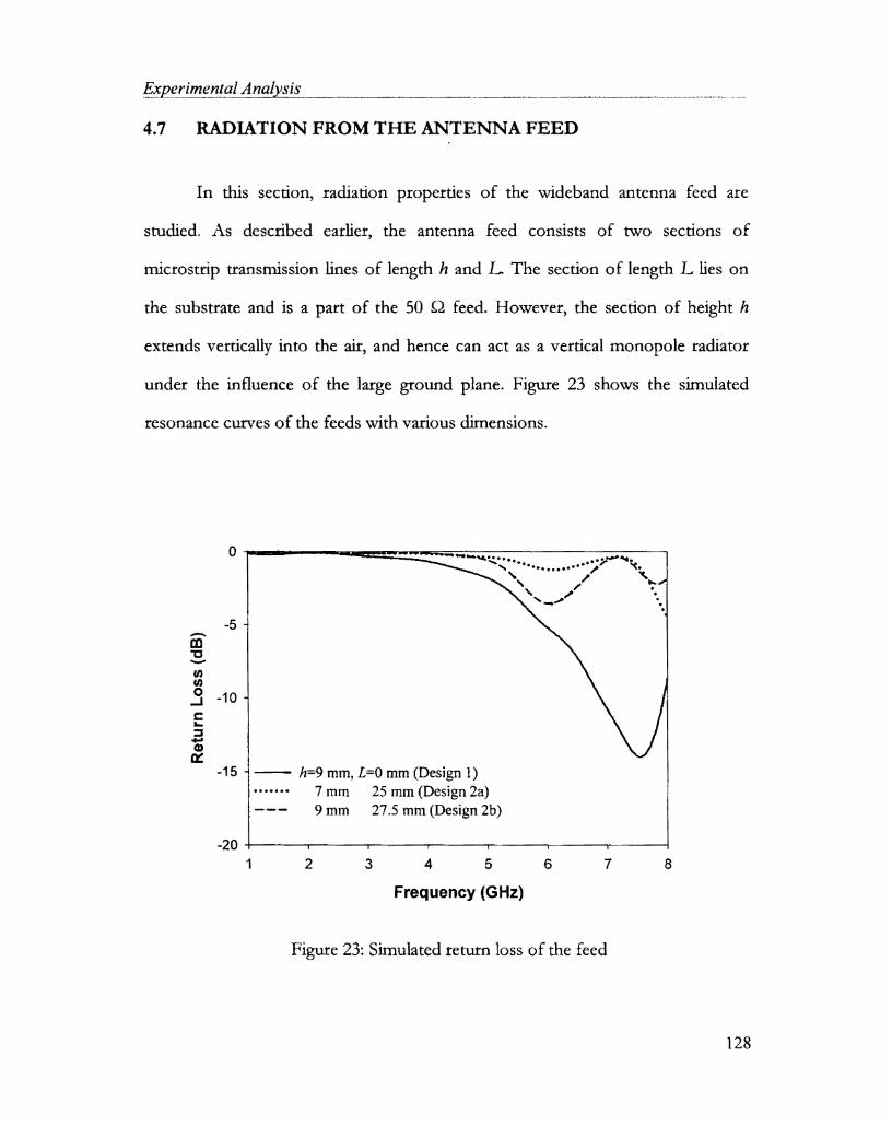
4.7 RADIATION FROM THE ANTENNA FEED
In this section, radiation properties of the wideband antenna feed are
studied. As described earlier, the antenna feed consists of two sections of
microstrip transmission lines of length h and L The section of length L Lies on
the substrate and is a part of the 50 £2 feed. However, the section of height h
extends vertically into the air, and hence can act as a vertical monopole radiator
under the influence of the large ground plane. Figure 23 shows the simulated
resonance curves of the feeds with various dimensions.
0 ....~_; 2 1“ . . . ' O Q .Q",'.~Q§\ O 0 0 0 . . . I ' ' . 0 Oob)’ x‘\ / vs ii\\ / '7’?I \ ‘.0
(dBReturn Loss
-10 _
-15 —- h=9 mm, L=0 mm (Design 1)---- -- 7 mm 25 mm (Design 2a)f —-— 9 mm 27.5 mm (Design 2b)
-20 -| ** | t F" - r —— l—‘ ~ I -— r |1 2 3 4 5 6 7 8Frequency (G Hz)
Figure 23: Simulated return loss of the feed
128

Chapter 4
As can be observed from the figure, a -14 dB deep resonance exists at
7.55 GHZ for the feed of design 1 (h = 9 mm, L = O mm). This value is
approximately equal to the resonant frequency of a k/ 4 monopole of length h I 9
mm. Simulated 3-D radiation pattern at 7.55 GHZ is given in Figure 24.
dD(a1 nTota1 )5 . 0@a0¢+aQ0
2. Beiem-BBO
7-1. aoaeQ+aoa
‘--». aoee=+-zoo
-:r.aeea-.-=+-sea
-1 . DB8-0-ml
Figure 24: Simulated radiation pattern of the feed at 7.55 GHZ
As observed from the above figure, the radiation pattern is not of a well
defined shape, so that it can hardly be used for any application purpose. This
monopole radiation can influence the radiation performance of the DRA if the
operating band includes the monopole’ band also, which could happen when using
DRs with low value of dielectric constant This is because, firstly, a higher
value of h will be needed for better impedance matching of a low std DR, and
hence the monopole resonance will occur at a frequency lower than that in the
present case (h = 9 mm). Secondly, the DR will operate at a higher frequency
because of the low 5,. Consequence is an effective resonating band, merged by the
individual bands of the DR and the monopole at the lower and the higher ends
129
l.’-‘Z2<.z2.@.:' ¢vIal.<1z1.q£1/§i§..--.. —— ._.,-- W“.-~-»---.... _,_ 4 4-»~ — -W 7 .~—'——~ ~~' _~. 774--V 1. -..__,. ...- ,.-..~ - ...,lm _ _ ..... -.._. ..___...._._ .,.-_..-._________ - ...____._.-.-_:--- _..-.-__._;,;.-.;.'.<;_:77-77.. -..--... .
respectively, with the radiation pattern distorted towards the higher end of the
band.
4.8 WIDEBAN D DESIGN USING OTHER DRs —- RESULTS
Validity of the wideband design (Design 2) is verified using other DRs also
having parameters as follows:
(1) DR-2: erd = 20.8, diameter 2a = 27.3 mm or 0.24 /lo and thickness d = 8.4 mm
or 0.074 10, /10 being the free space wave length corresponding to the measured
broadside mode frequency, f = 2.65 GHZ of the DRA.
(2) DR-3: std I 88.68, diameter 2a = 24 mm or 0.166 /is and thickness d = 7.8 mm
or 0.054 /lo, /in corresponds to the measured broadside mode frequency, f = 2.04
GHZ of the DRA.
The antennas using the above DRs (1) and (2) will be referred respectively
as DRA-1 and DRA-2 in the following discussion. HFSSTM simulation is used to
optimise the design parameters to yield maximum matching bandwidth and the
simulated return loss plots are presented in Figures 25 and 26 respectively for
DRA-2 and DRA-3. Tuning of the impedance characteristics is appealing from
Figures 25(a) and 26(a). For DRA-2, selection of h = 10 mm and L = 31 mm
gives a bandwidth from 1.9 to 2.65 GHZ or 33 °/0. Measured return loss is
compared with the simulated one in Figure 25(b). A matching band from 1.849 to
2.549 GHZ or 32 % is obtained for the measurement. This band covers some
important wireless communication bands like PCS (1.85 to 1.99 GHZ), UMTS (1.9
130

. .............. - -.Qf_1a2f er 4to 2.2 GHZ), \X/iBro (2.3 to 2.39 GHZ) and WLAN (ISM: 2.4 to 2.484 GHZ)
[Table 2, Chapter 1]. The above figure also shows two merged resonances, at 1.9
GI-lz and 2.41 GI-Iz constituting the matching band.
For DRA-3, a maximum simulated bandwidth of 11.15 % is achieved for h
= 5 mm and L = 30 mm, while the measured band is from 1.835 to 2.125 GHz or
14.65 °/o. This band covers the PCS and some part of the IMTS and UMTS bands.
Corresponding plots are shown in Figure 26.
Measured conical radiation patterns for DRA-2 and DRA-3 are shown in
Figure 27 and 28 respectively. Note that the radiation patterns at the two
resonances, at 1.9 GHZ and 2.41 GHz for DRA-2 are shown in Figure 27,
revealing that both resonances have the same radiation characteristics. Measured
gain is 3.74 dBi at 1.9 GHz and 3.95 dBi at 2.41 GI-lz. Also the maximum
measured gain in the band is 4.71 dBi, at 2.3 GHZ. For DRA-3, the radiation
patterns at 1.945 GI-Iz, which is the frequency giving minimum reflection and also
is the mid-band frequency, are plotted in Figure 28. Gain measurement yielded a
maximum gain of 3.88 dBi at 1.945 GHZ, for DRA-3.
131

€2§2§[email protected]@l.1%£i§.--------_%_=__-_—:—~_- —— — —~—— —-Afr’:--_-_-_—— —— — ————-—— —~ —-——----=.—_—_-.7.-_»_'* -.-.~..-.».~.-».-.w.-1.----..|-..,-.....--.,-»¢~
\ I \. '0 5'.‘ ‘I 'I ‘ 2 I ‘~. ~'\ / \ \ I .' I .— \//fl_\\_¢ I.---.'\_,,/. ..'°-, '3 1-". 1
Return Loss (dB)
2
.\_
/"
.|_n‘-20 _ I? Q.I 11 —-————- h=4 mm, L=l3 mm g ,_30 _ ........... .. 6 mm 2] mm r—--—--—-- 8 mm 27 mm @—---—~-' 10 mm 31 mm‘,-—-—- 12mm 34mm 1
-40 6 f_* r *1 ‘ -1 " -'1 6*: 6 1 " l * I0.4 0.8 1.2 1.6 2.0 2.4 2.8 3.2 3.6 4.0
A L’ "\_ __,...\
Frequency (GHz)(8)0 ______ - ,CV \\ /12-5 _ \ .. X /-10 \ ____ /154 1 J k
Return Loss (dB)
-20 _-25 ii I , I_30 * * -———— Measured—-——- HFSS
-35 '— t" * 1 — 1 ‘ l_*' 1 6‘ *1 |1.4 1.6 1.8 2.0 2.2 24 26 28 30Frequency (GHz)
(b)
Figure 25: (a) Simulated return loss of DRA-2 for various h and L
(b) Measured and simulated return loss for h = 10 mm and L = 31 mm
132
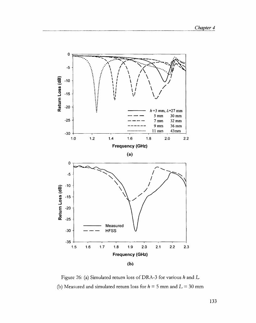
_____________________ .................. ..__..............._.... ..... -._.__...............- Q1“ F" ff
Return Loss (dB)Return Loss (dB)
Figure 26: (a) Simulated return loss of DRA-3 for various h and L
(b) Measured and simulated return loss for h = 5 mm and L = 30 mm
5-25 J
-19 _
_15 -14
2o~ =
T7. ii ‘-\ "9-K Y,‘-L.‘ _.“'\ ‘
‘-4L itiii“'&‘
\\l\ /1\! \ /h =3 mm, L=27 mm
mm 30 mm7 mm 32 mm9 mm 36 mm
-30 M jll 7_ T ‘M “|u.N._¢-.:--- l nu-n t__43n-In]
-15 ~
-20 ~
'. . "' "*¢ '“'~<-5 .. \\ I/‘<\ \ /‘\1 ' \\ 1 \ ' X,\ I \ *1 /\ \_/
1.0 1.2 1.4 1.6
O
Frequency (GHz)
(3)
1.8 2.0 2 2
25:Measured
-30 - — --— — HFSS
-35 -‘ewe .e F" . ~ . . .1.5 1.6 1.7
/"\-5‘ \\ I xx\ / \101 \ /\ /\ // 1
1.8 1.9 2.0 2.1 2.2 2 3Frequency (GI-lz)
(b)

ExpecimenwliA~9b*siS__W {{{{{{{{{{{{{{{{{{{{{ ( _,__-- -~ ---Q..--,_—_—.—..'_:::;r—_: ,--~-_--_--._-—_:—..-;__-—.:i:_1—— ~ -'A~ -.--%~;~-7;--V
XZ-planeso120 ; so
,»"5”._'“\ Z "" ,‘ _¢ .. 0 L L. ;/ \ 2150 /Rb _%\ _ so‘ _-.. /' : ";.|.:o§0..$.é .
d,¢r""'-..__ /,v'T~ \§
I. ,_/-\--. ./..II..Q..... I‘ ._\. .... 0.‘ ,-~" ""-_ I' 0 w -\9/ 1 '\"- I‘qlOI'_00u.":. I‘ .'-:. . I‘ , -I ;-(‘*3r '».<9.~' ¢>
2:. ..'u 0\.O.o'......0' I ‘ , b 0....‘-"0'. ‘A II 5.‘ ._ '’ "~/.. \ .\. ’ Q
\ -\__ _c,' "N .'..x'\-_h;¥;aHH g‘:==L:¢f@-1€ - \. - = \~_“______“'Q) .0° .QQ
180 \ . .} | .4\ \\; , ,_ 1 _;R: {it f,-_{“fi.%d‘\\
210 \\ *\\ . - . . .'-“'- . Q. .-"*1, /\\ 1. g _ _ I, ' : Q i - \aj ‘I'D’ ii’240 E 300
270 W-——— 1.9 GHz C0-polar—- — -— 1.9 GHz Cross~polar———— —- 2.41 GHz Co-polar---~-~~--- 2.41 GHz Cross-poiar
YZ-plane
so120 ? 60‘ _Q..§_ __
‘I-,aI¢"—"OI§
4!’ iT;;:\5§i::€t;;h::fG_~.-_ '\ kon x ooogu... fl
)\r M\\ 'f Jjég9 5 ‘ - .- .U’ 0.. /_.,\_. ._ .: 55:0._ - "Ix ’, . \\ //_ .. In" I \_\_ \ -.. C...;\. .’._:..... ‘T\ \
" ‘Sf.
1' "-Q;H&a-0
O0(AlO
150 . _20%,. L If so
-,0!’
. ‘ _ -_180 . _ . ,. . . . . I 0_ , . . g. /\ , _\
\ '.\
00000 — ..
" '_ \ ‘I, l 1 - ‘..\_'._ *' .0' -_¢|...... - '- : X240 aoo
210
Figure 27: Measured radiation patterns for DRA-2

- ...... ,.__...,,,.,.._,,,,..,,..,.,.,.,,,_,,,. ......... ._.-_--.“-—~_=_-:_—_—_—:__—-—»---.~ ~ ~ -_—_-V-_:_-_=~.—_-.-.—.-.%-.-.-+--.--1-' ' " ' "_ _ ~_,_'<-,.p-\¢q,¢---' _ : .—1-_—_-_1_->_-_-\--.---.--.--_“-¢~v~.---w~v-~_-.-...
XZ-plane90120 ’ so
". .' I D \
-A01Q
ii?Q
/"
u:Q
/_-_\* ,_\ ‘ _____‘,\. 0;... fi/ \‘</ / ‘. _\ \ 4- I, ._ .180 Mummm ‘mmW,WmWmH§W,4Q;;§QMHm} .mmmH‘.“. 0
‘\
I \ __ ~\ _ '~' _. -\ , . \. >210 \ ,-K | 330240 300
270
——-% 1.945 GHz_Co-polar— — - - 1.945 GHz Cross-polar
YZ-plane90120 ' f so
,10W;m_,1s0 ' ./ R-ix ‘ so'~ I, 'v.f2 '5 * \\ “
E _ 'E'/180 .m. . HH{?.. §.‘4b§%3f Wm_ “(.. ".mHM. O
--""
' ,':=-.‘.
w Z, I "~§ \/210 ‘~ V ‘ 330L§§ § ’§r, -\_ /
240 5 300270
Figure 28: Measuxcd radiation patterns for DRA-3
Cf?§avI@rfZ
135

_Hm_g® NV" mCBBNQ Om Hg gang HUHOfi@HQ@w Om Ugiw gm UEWQ Eaasmwoa WHO 5 “BBQU: an: W $09 om W Ewv awv _Am“? Mg A _ 58302}_ C L Sbmfiv XN _ % %“‘ ‘I ‘ ‘ ‘ :\‘ E ‘ l“|‘\\‘:‘_|woaamg j w§£r_ 08%| 7_:___ _26_ _ _Vo_~__ _o<n_ _LO aw ga _Aomnv __\__V ‘ ll} _ 1 IHug”§_g°__ _&_g%__Q9 Una03$? _§ j_O<G_ F §_§ may_ M:HRS“ % an { XN HQXN §gagQMNgfixmafiaM55 F HE"UWDQagU§-NANO_w_Na_m_A_W ww _ A % Aab:__glN_w_@ 3 ‘Nari E__N( Lao LgA Go:0I; ‘go V:_ NR: % 'N$© INRTNO '5 _;gaw E0 _I; _8_$ P3\\_ ‘_$3_ Ag NWOTQVUPHWQAmm_&_N£_m_ . _ $3 ‘NO L __m ISO LtE “:8 _2% I N Hgg_&u l‘hL_| w_|| T‘! ‘ I‘ ‘ 1|‘TaVaE %_:_: ‘E gm AmzbaQINV“Er: _ ‘_a

4.9 RADIATION EFFICIENCY
Radiation efficiencies of the DRAs are measured using the Wheeler cap
method (Section 3.10.4, Chapter 3). A cylindrical metallic cap of diameter = 17 cm
and height = 7.5 cm was used as the radiation shield, for the DR_A. Measured
efficiencies in the respective operating bands are given in Table 4.
Table 4: Measured radiation efficiencies of the DRAs so far studied(dimensions are in ‘mm’)
' 1 —* —' ~ < — v ~' t — — 7' ' 1- —' ' — 1‘DRA Broadside Designl i Design 2a I Design 2b I DRA-2 DRA-3_ I l , , , l_ .__ ll _ __ _l _ lI he - 1" R R ~ ~ — — — i ie I ~ — 1 JI l l l
(ad, 24, d, ~ (20.s,24,7.3 (20.s,24,7.s (20.s,24,7.3 I (20.s,24,7.3 (20.s,27.3,s.4 A (ss.(>s,24,7.s ,h L) -,-) I 9,-) 7, 25) 9,275) A, 10,3125) 5,30)l l _ __~ - l o F l ‘ t o o l1l“d‘?“°“ 85.3 96.24 93.07 92.85 I 91.65 , 76.08Efficiency y_ t(°/0) A 1 T t t I A l l
From the above table, it can be made out that the wideband design offers
higher radiation efficiency than the fundamental design of a cylindrical DR. Also it
is deduced that the DR with low er is a better radiator than that with high 2,, since
the energy storage is more in the case of the latter. However, promising size
reduction can not be achieved with a lower er DR, unless special design rules are
followed. Thus, when the use of a DR as an antenna is concerned, the choice of 6,
is as per the requirement of the antenna engineer.
137

_4.10 WIDEBAND DESIGN USING A DIFFERENT SUBSTRATE
In order to confirm the suitability of the wideband design (design 2) with
different substrate for the feed, the DRA is simulated using a 50 mrn x 4.93 mm
microstrip line formed on a 1.6 mm thick RT/Duroid substrate of at = 2.2. The
feed was designed using Eq. 3.21 and 3.22 in Chapter 3. The DR parameters are,
at = 20.8, 2a = 24 mm and d = 7.3 mm, the same as those of DR-1. The -10 dB
impedance bands, almost the same as those obtained on the er = 4 substrate, are
found here also as,
Band 1: 2.43 to 3.45 GHZ, for h = 7 mm, L = 31.5 mm
Band 2: 2.1 to 2.91 GHZ, for h = 9 mm, L = 37 mm as shown in Figure 29.
0 ' “'\ 5 — T\ // “'-5 / \“ \ /-- \ /10 \\ //hf
Return Loss d
—15f \ /1 \/\./'
_20 _
i h=7 mm L=3l.5 mm— — — h=9 mm L=37 mm-25 1 | t—"* — 9» +~ —~—s~. .1.5 2.0 2.5 3.0 3.5 4.0
Frequency (GHz)
Figure 29: Simulated return loss of the wideband DRA excited by a
microstrip feed on an RT/Duroid substrate
138

CONCLUSION
Development of a wideband cylindrical DRA was presented with the help
of measurements using I-IP 8510C vector network analyser and simulations using
Ansoft HFSSTM. A bandwidth in excess of 30 °/o with stable conical radiation
pattern and good gain was obtained for the proper design. High radiation
efficiencies in excess of 90 % were obtained, due to the inherent low loss of the
DR. Effect of various design parameters on the DRA performance was also
studied. The mid-band frequency of the operating band can be tuned by changing
the topological and/ or material properties of the DRA. However, medium
permittivity DRs are preferred for the design, since they provide wider
bandwidths, better gains and higher radiation efficiencies than high permittivity
DRs.
139

€2s2¢rim@n.!ql.A;nalJ.%§§§.. (((((((((((((((((((((( r %%%%%%%%%%%%% ........... ..
REFERENCES
[1] High Frequency Structure Simulator (HFSS), Ansoft Corporation, Pittsburgh,
PA
[2] R. A. Kranenburg and S. A. Long, Microstrip Transmission Line Excitation of
Dielectric Resonator Antennas, Electro. Lett., Vol. 24, pp. 1156-1157, january
1988
[3] K. W. Leung, K. Y. Chow, K. M. Luk and E. K. N. Yung, Low-profile
Circular Disk DR Antenna of Very High Permittivity Excited by a Microstrip
Line, Electro. Lett., Vol. 33,pp. 1004-1005,]une 1997
[4] C. S. De Young and S. A. Long, Wideband Cylindrical and Rectangular
Dielectric Resonator Antennas, IEEE Anten. Wireless Propagat. Lett., Vol. 5,
pp. 426-429, 2006
[5] D. Kajfez, A. W. Glisson and James, Computed Modal Field Distributions
for Isolated Dielectric Resonators, IEEE Trans. Microwave Theory Tech.,
V0132 ,pp. 1609-1616, December 1984
[6] R. K Mongia and P. Bhartia, Dielectric Resonator Antennas—A Review and
General Design Relations for Resonant Frequency and Bandwidth, Inter.
journal of Microwave and Millimeter-Wave Comp. aided Eng., Vol. 4, pp.
230-247,]uly 1994
[7] K. Lan, S. K. Chaudhmy and S. Safavi-Naeini, Design and Analysis of A
Combination Antenna with Rectangular Dielectric Resonator and inverted L
Plate, IEEE Trans. on Antennas Propagat, Vol. 53, pp. 495-501, January 2005
140