Embed Size (px)
Citation preview
www.ti.com
FEATURES
APPLICATIONS
1
2
3
4
5
6
7
8
9
10
11
12
13
14
28
27
26
25
24
23
22
21
20
19
18
17
16
15
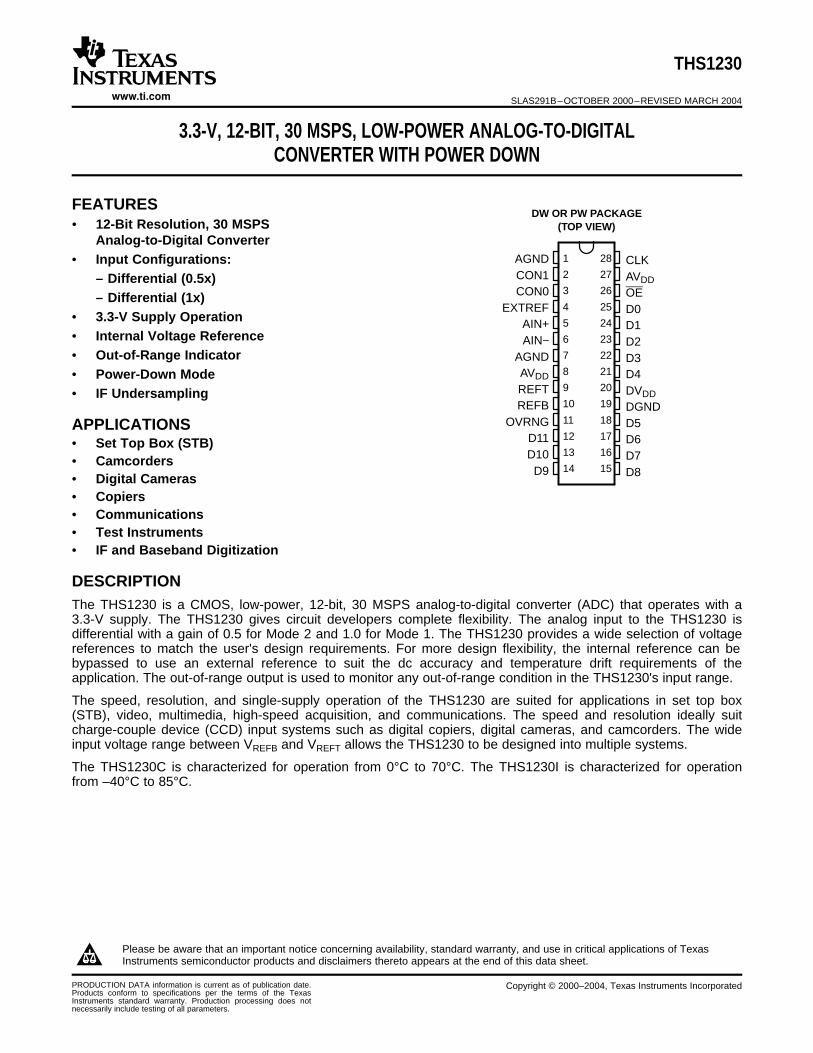
AGNDCON1CON0
EXTREFAIN+AIN−
AGNDAVDD
REFTREFB
OVRNGD11D10
D9
CLKAVDDOED0D1D2D3D4DVDDDGNDD5D6D7D8
DW OR PW PACKAGE(TOP VIEW)
DESCRIPTION
THS1230
SLAS291B–OCTOBER 2000–REVISED MARCH 2004
3.3-V, 12-BIT, 30 MSPS, LOW-POWER ANALOG-TO-DIGITALCONVERTER WITH POWER DOWN
• 12-Bit Resolution, 30 MSPSAnalog-to-Digital Converter
• Input Configurations:– Differential (0.5x)– Differential (1x)
• 3.3-V Supply Operation• Internal Voltage Reference• Out-of-Range Indicator• Power-Down Mode• IF Undersampling
• Set Top Box (STB)• Camcorders• Digital Cameras• Copiers• Communications• Test Instruments• IF and Baseband Digitization
The THS1230 is a CMOS, low-power, 12-bit, 30 MSPS analog-to-digital converter (ADC) that operates with a3.3-V supply. The THS1230 gives circuit developers complete flexibility. The analog input to the THS1230 isdifferential with a gain of 0.5 for Mode 2 and 1.0 for Mode 1. The THS1230 provides a wide selection of voltagereferences to match the user's design requirements. For more design flexibility, the internal reference can bebypassed to use an external reference to suit the dc accuracy and temperature drift requirements of theapplication. The out-of-range output is used to monitor any out-of-range condition in the THS1230's input range.
The speed, resolution, and single-supply operation of the THS1230 are suited for applications in set top box(STB), video, multimedia, high-speed acquisition, and communications. The speed and resolution ideally suitcharge-couple device (CCD) input systems such as digital copiers, digital cameras, and camcorders. The wideinput voltage range between VREFB and VREFT allows the THS1230 to be designed into multiple systems.
The THS1230C is characterized for operation from 0°C to 70°C. The THS1230I is characterized for operationfrom –40°C to 85°C.
Please be aware that an important notice concerning availability, standard warranty, and use in critical applications of TexasInstruments semiconductor products and disclaimers thereto appears at the end of this data sheet.
PRODUCTION DATA information is current as of publication date. Copyright © 2000–2004, Texas Instruments IncorporatedProducts conform to specifications per the terms of the TexasInstruments standard warranty. Production processing does notnecessarily include testing of all parameters.

www.ti.com
FUNCTIONAL BLOCK DIAGRAM
12-Bit ADC D[11:0]Sampleand Hold
CLK
DGNDAGND
OVRNG
CON0
Timing Circuitry
REFT REFB
InternalReference
Circuit
CON1
3-StateOutputBuffers
EXTREF
ConfigurationControlCircuit
DVDD
AIN+
AIN−
AVDD
OE
THS1230
SLAS291B–OCTOBER 2000–REVISED MARCH 2004
This integrated circuit can be damaged by ESD. Texas Instruments recommends that all integratedcircuits be handled with appropriate precautions. Failure to observe proper handling and installationprocedures can cause damage.
ESD damage can range from subtle performance degradation to complete device failure. Precisionintegrated circuits may be more susceptible to damage because very small parametric changes couldcause the device not to meet its published specifications.
ORDERING INFORMATION
PRODUCT PACKAGE- PACKAGE SPECIFIED PACKAGE ORDERING TRANSPORT MEDIA,LEAD DESIGNATOR (1) TEMPERATURE MARKING NUMBER QUANTITY
RANGE
THS1230 TSSOP-28 PW 0°C to 70°C TH1230 THS1230CPW Tube, 50
THS1230 TSSOP-28 PW 0°C to 70°C TH1230 THS1230CPWR Tape and reel, 2000
THS1230 TSSOP-28 PW -40°C to 85°C TJ1230 THS1230IPW Tube, 50
THS1230 TSSOP-28 PW -40°C to 85°C TJ1230 THS1230IPWR Tape and reel, 2000
THS1230 SOP-28 DW 0°C to 70°C TH1230 THS1230CDW Tube, 20
THS1230 SOP-28 DW 0°C to 70°C TH1230 THS1230CDWR Tape and reel, 1000
THS1230 SOP-28 DW -40°C to 85°C TJ1230 THS1230IDW Tube, 20
THS1230 SOP-28 DW -40°C to 85°C TJ1230 THS1230IDWR Tape and reel, 1000
(1) For the most current specifictions and package information refer to our Web site at www.ti.com.
2

www.ti.com
TERMINAL FUNCTIONS
ABSOLUTE MAXIMUM RATINGS (1)
THS1230
SLAS291B–OCTOBER 2000–REVISED MARCH 2004
TERMINALI/O DESCRIPTION
NAME NO.
AGND 1, 7 I Analog ground
AVDD 8, 27 I Analog supply
AIN+ 5 I Positive analog input
AIN- 6 I Negative analog input
CLK 28 I ADC conversion clock
CON1 2 I Configuration input 1
CON0 3 I Configuration input 0
DGND 19 I Digital ground
DVDD 20 I Digital supply
D11 12 O ADC data bit 11
D10 13 O ADC data bit 10
D9 14 O ADC data bit 9
D8 15 O ADC data bit 8
D7 16 O ADC data bit 7
D6 17 O ADC data bit 6
D5 18 O ADC data bit 5
D4 21 O ADC data bit 4
D3 22 O ADC data bit 3
D2 23 O ADC data bit 2
D1 24 O ADC data bit 1
D0 25 O ADC data bit 0
EXTREF 4 I Reference select input (high = external, low = internal)
OVRNG 11 O Out of range indicator (high = out of range)
OE 26 I Output enable (high = disable, low = enable)
REFT 9 I/O Upper ADC reference voltage
REFB 10 I/O Lower ADC reference voltage
over operating free-air temperature range (unless otherwise noted)
UNIT
AVDD to AGND, DVDD to DGND –0.3 V to 4 VSupply voltage range
AGND to DGND –0.3 V to 0.3 V
Reference voltage input range, REFT, REFB to AGND –0.3 to AVDD + 0.3 V
Analog input voltage range, AIN+, AIN- to AGND –0.3 to AVDD + 0.3 V
Clock input voltage range, CLK to AGND –0.3 to AVDD + 0.3 V
Digital input voltage range, digital input to DGND –0.3 to DVDD + 0.3 V
Digital output voltage range, digital output to DGND –0.3 to DVDD + 0.3 V
Operating junction temperature range, TJ –40°C to 150°C
Storage temperature range, TSTG – 65°C to 150°C
Lead temperature 1,6 mm (1/16 in) from case for 10 seconds 300°C
(1) Stresses beyond those listed under "absolute maximum ratings" may cause permanent damage to the device. These are stress ratingsonly, and functional operation of the device at these or any other conditions beyond those indicated under "recommended operatingconditions" is not implied. Exposure to absolute-maximum-rated conditions for extended periods may affect device reliability.
3

www.ti.com
RECOMMENDED OPERATING CONDITIONS
THS1230
SLAS291B–OCTOBER 2000–REVISED MARCH 2004
over operating free-air temperature range, TA (unless otherwise noted)
MIN NOM MAX UNIT
POWER SUPPLY
Supply voltage AVDD 3.0 3.3 3.6 VDVDD
ANALOG AND REFERENCE INPUTS
Reference input voltage VREFT fCLK = 5 MHz to 30 MHz 2.0 2.15 2.5 V
VREFB fCLK = 5 MHz to 30 MHz 1.05 1.15 1.3
Reference voltage differential, VREFT – VREFB fCLK = 5 MHz to 30 MHz 0.95 1.0 1.05 V
Analog input voltage differential, (AIN+) – (AIN–) (1) CON1 = 0, CON0 = 1 –1.0 1.0 V
CON1 = 1, CON0 = 0 –2.0 2.0
Analog input capacitance, Ci 10 pF
Clock input (2) 0 AVDD V
DIGITAL OUTPUTS
Minimum digital output load resistance, RL 100 kΩ
Maximum digital output load capacitance, Ci 0 10 15 pF
DIGITAL INPUTS
High-level input voltage, VIH 2.4 DVDD V
Low-level input voltage, VIL DGND 0.8 V
Clock frequency, fCLK(3) 5 30 MHz
Clock pulse duration, tw(CLKL), tw(CLKH) fCLK = 30 MHz 15 16.7 18.3 ns
Operating free-air temperature, TA TH1230 0 70 °C
TJ1230 –40 85
(1) Based on VREFT – VREFB = 1.0 V, varies proportional to the VREFT – VREFB value. AIN+ and AIN– inputs must always be greater than 0 Vand less than AVDD.
(2) Clock pin is referenced to AGND and powered by AVDD.(3) Clock frequency can be extended to this range without degradation of performance.
4
www.ti.com
ELECTRICAL CHARACTERISTICS
THS1230
SLAS291B–OCTOBER 2000–REVISED MARCH 2004
over recommended operating conditions (AVDD = DVDD = 3.3 V, fs = 30 MHz/50% duty cycle, MODE = 1, 1-V input span,internal reference, Tmin to Tmax) (unless otherwise noted)
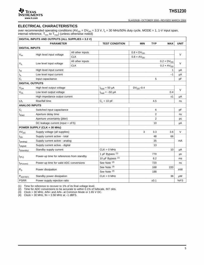
DIGITAL INPUTS AND OUTPUTS (ALL SUPPLIES = 3.3 V)
PARAMETER TEST CONDITION MIN TYP MAX UNIT
DIGITAL INPUTS
All other inputs 0.8 × DVDDVIH High level input voltage VCLK 0.8 × AVDD
All other inputs 0.2 × DVDDVIL Low level input voltage VCLK 0.2 × AVDD
IIH High level input current 1 µA
IIL Low level input current –1 µA
Ci Input capacitance 5 pF
DIGITAL OUTPUTS
VOH High level output voltage Iload = 50 µA DVDD–0.4V
VOL Low level output voltage Iload = –50 µA 0.4
High impedance output current ±1 µA
tr/tf Rise/fall time CL = 10 pF 4.5 ns
ANALOG INPUTS
Ci Switched input capacitance 6 pF
td(ap) Aperture delay time 2 ns
Aperture uncertainty (jitter) 2 ps
DC leakage current (input = ±FS) 10 µA
POWER SUPPLY (CLK = 30 MHz)
XVDD Supply voltage (all supplies) 3 3.3 3.6 V
IDD Supply current active - total 48 66
I(analog) Supply current active - analog 35 mA
I(digital) Supply current active - digital 13
II(standby) Standby supply current CLK = 0 MHz 10 µA
1 µF Bypass (1) 770 µst(PU) Power-up time for references from standby
10 µF Bypass (1) 6.2 ms
t(PUconv) Power-up time for valid ADC conversions See Note (2) 720 ns
See Note (3) 168 220PD Power dissipation mW
See Note (4) 188
PD(STBY) Standby power dissipation CLK = 0 MHz 36 µW
PSRR Power supply rejection ratio ±0.1 %FS
(1) Time for reference to recover to 1% of its final voltage level.(2) Time for ADC conversions to be accurate to within 0.1% of fullscale, INT ckts.(3) Clock = 30 MHz, AIN+ and AIN– at Common Mode or 1.65 V DC.(4) Clock = 30 MHz, fin = 3.58 MHz at –1 dBFS.
5

www.ti.com
ELECTRICAL CHARACTERISTICS (CONTINUED)
1.5 VBANDGAP
REFT
REFB
CT
CB
CTB
THS1230
THS1230
SLAS291B–OCTOBER 2000–REVISED MARCH 2004
over recommended operating conditions (AVDD = DVDD = 3.3 V, fs = 30 MHz/50% duty cycle, MODE = 1, 1-V input span,internal reference, Tmin to Tmax) (unless otherwise noted)
REFT, REFB REFERENCE VOLTAGES (all supplies = 3.3 V)
PARAMETER TEST CONDITION MIN TYP MAX UNIT
INTERNAL REFERENCE (1)
VREFT Upper reference voltage 2.15
VREFB Lower reference voltage 1.15 V
VREF Differential reference voltage, VREFT – VREFB 0.95 1 1.05
Differential reference voltage, VREFT – VREFB accuracy –5% 5%
EXTERNAL REFERENCE
Externally applied VREFT reference voltage range 2 2.5
Externally applied VREFB reference voltage range 1.05 1.3 V
Externally applied (VREFT – VREFB) reference voltage range 0.75 1.05
External mode VREFT to VREFB impedance 9 kΩ
INTERNAL OR EXTERNAL REFERENCE
CT VREFT decoupling capacitor value 0.1
CB VREFB decoupling capacitor value 0.1 µF
CTB Decoupling capacitor VREFT to VREFB 10
(1) The internal reference voltage is not intended for use driving off chip.
Figure 1. Reference Generation
6
www.ti.com
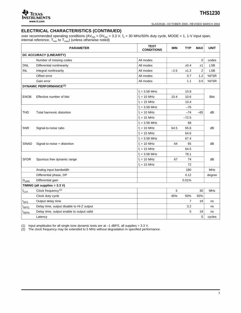
ELECTRICAL CHARACTERISTICS (CONTINUED)
THS1230
SLAS291B–OCTOBER 2000–REVISED MARCH 2004
over recommended operating conditions (AVDD = DVDD = 3.3 V, fs = 30 MHz/50% duty cycle, MODE = 1, 1-V input span,internal reference, Tmin to Tmax) (unless otherwise noted)
TESTPARAMETER MIN TYP MAX UNITCONDITIONS
DC ACCURACY (LINEARITY)
Number of missing codes All modes 0 codes
DNL Differential nonlinearity All modes ±0.4 ±1 LSB
INL Integral nonlinearity All modes –2.5 ±1.2 2 LSB
Offset error All modes 0.7 1.2 %FSR
Gain error All modes 1.1 3.5 %FSR
DYNAMIC PERFORMANCE (1)
fi = 3.58 MHz 10.9
ENOB Effective number of bits fi = 10 MHz 10.4 10.6 Bits
fi = 15 MHz 10.4
fi = 3.58 MHz –76
THD Total harmonic distortion fi = 10 MHz –74 –65 dB
fi = 15 MHz –72.5
fi = 3.58 MHz 68
SNR Signal-to-noise ratio fi = 10 MHz 64.5 65.6 dB
fi = 15 MHz 64.6
fi = 3.58 MHz 67.4
SINAD Signal-to-noise + distortion fi = 10 MHz 64 65 dB
fi = 15 MHz 64.5
fi = 3.58 MHz 78.1
SFDR Spurious free dynamic range fi = 10 MHz 67 74 dB
fi = 15 MHz 72
Analog input bandwidth 180 MHz
Differential phase, DP 0.12 degree
G(diff) Differential gain 0.01%
TIMING (all supplies = 3.3 V)
fCLK Clock frequency (2) 5 30 MHz
Clock duty cycle 45% 50% 55%
td(O) Output delay time 7 19 ns
td(PZ) Delay time, output disable to Hi-Z output 3.2 ns
td(EN) Delay time, output enable to output valid 5 19 ns
Latency 5 cycles
(1) Input amplitudes for all single tone dynamic tests are at –1 dBFS, all supplies = 3.3 V.(2) The clock frequency may be extended to 5 MHz without degradation in specified performance.
7

www.ti.com
PARAMETER MEASUREMENT INFORMATION
TIMING DIAGRAM
Analog
CLK
D[9:0] S1 S2 S3
S1 S2 S3
t d(O)
t PIPELINE
1 2 3 4 5 6 7 8 9 10
OE
D[9:0]
td(PZ)td(EN)
Hi−Z Hi−ZData Data Data
THS1230
SLAS291B–OCTOBER 2000–REVISED MARCH 2004
Figure 2. Analog Input and Data Output Timing
Figure 3. Output Enable Timing
8
www.ti.com
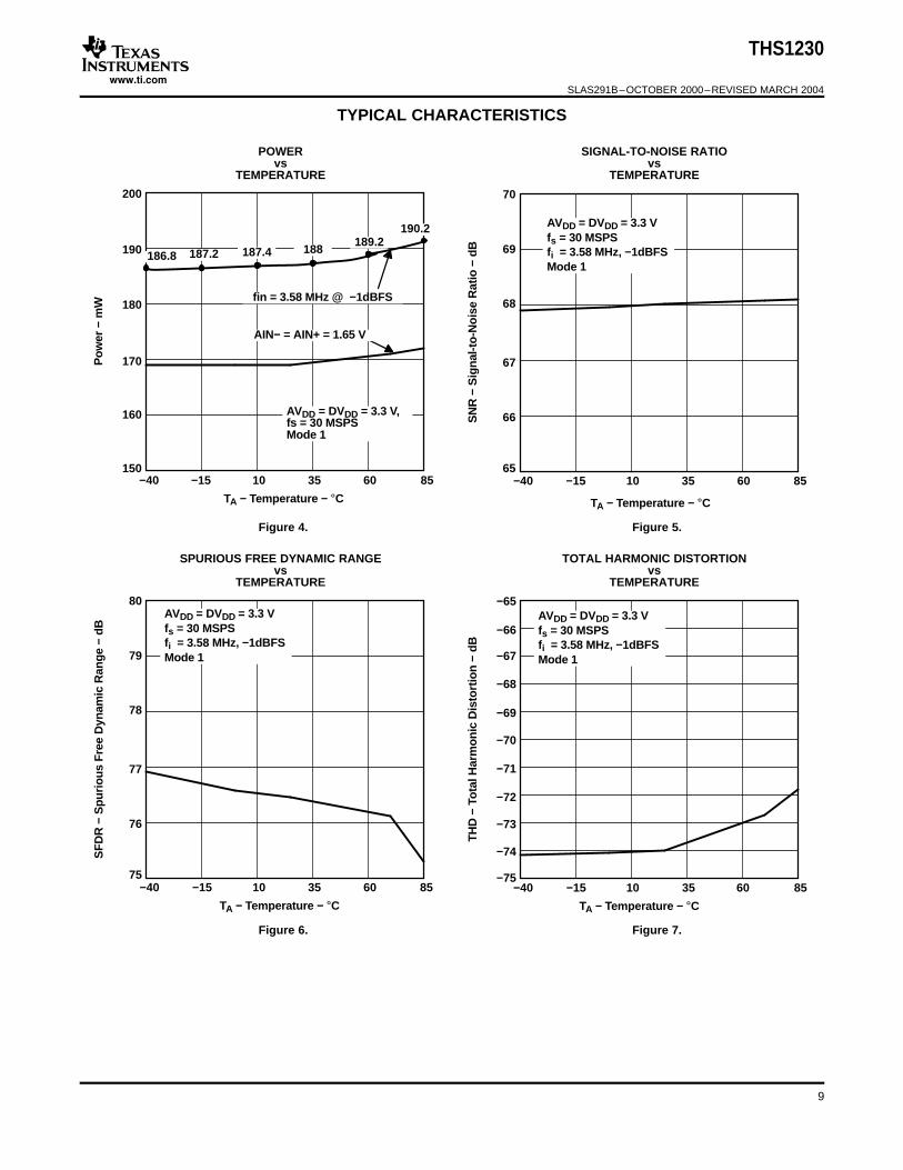
TYPICAL CHARACTERISTICS
170
160
150−40 −15 10 35 60 85
Po
wer
− m
W 180
190
200
TA − Temperature − °C
186.8 187.2 187.4 188189.2
190.2
fin = 3.58 MHz @ −1dBFS
AIN− = AIN+ = 1.65 V
AVDD = DVDD = 3.3 V,fs = 30 MSPSMode 1
67
66
65−40 −15 10 35 60 85
SN
R −
Sig
nal
-to
-No
ise
Rat
io −
dB
68
69
70
AVDD = DVDD = 3.3 Vfs = 30 MSPSfi = 3.58 MHz, −1dBFSMode 1
TA − Temperature − °C
77
76
75−40 −15 10 35 60 85
SF
DR
− S
pu
rio
us
Fre
e D
ynam
ic R
ang
e −
dB
78
79
80
TA − Temperature − °C
AVDD = DVDD = 3.3 Vfs = 30 MSPSfi = 3.58 MHz, −1dBFSMode 1
−68
−69
−70
−71
−40 −15 10 35 60 85
TH
D −
To
tal H
arm
on
ic D
isto
rtio
n −
dB
−67
−66
−65
−74
−75
−73
−72
TA − Temperature − °C
AVDD = DVDD = 3.3 Vfs = 30 MSPSfi = 3.58 MHz, −1dBFSMode 1
THS1230
SLAS291B–OCTOBER 2000–REVISED MARCH 2004
POWER SIGNAL-TO-NOISE RATIOvs vs
TEMPERATURE TEMPERATURE
Figure 4. Figure 5.
SPURIOUS FREE DYNAMIC RANGE TOTAL HARMONIC DISTORTIONvs vs
TEMPERATURE TEMPERATURE
Figure 6. Figure 7.
9
www.ti.com
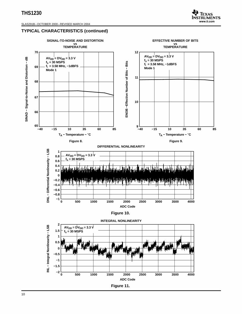
67
66
65−40 −15 10 35 60 85
SIN
AD
− S
ign
al-t
o-N
ois
e an
d D
isto
rtio
n −
dB
68
69
70
TA − Temperature − °C
AVDD = DVDD = 3.3 Vfs = 30 MSPSfi = 3.58 MHz, −1dBFSMode 1
9−40 −15 10 35 60 85
EN
OB
−E
ffec
tive
Nu
mb
er o
f Bits
− B
its
10
11
12
TA − Temperature − °C
AVDD = DVDD = 3.3 Vfs = 30 MSPSfi = 3.58 MHz, −1dBFSMode 1
0.4
0.2
0 500 1000 1500 2000 2500 3000DN
L −
Diff
eren
tial N
on
linea
rity
− L
SB
0.6
0.8
ADC Code
1
3500 4000
−0.4
−0.6
−0.2
0
−0.8−1
AVDD = DVDD = 3.3 Vfs = 30 MSPS
0.5
0
0 500 1000 1500 2000 2500 3000
INL
− In
teg
ral N
on
linea
rity
− L
SB
1
1.5
ADC Code
2
3500 4000
−1.5
−2
−1
−0.5
AVDD = DVDD = 3.3 Vfs = 30 MSPS
THS1230
SLAS291B–OCTOBER 2000–REVISED MARCH 2004
TYPICAL CHARACTERISTICS (continued)
SIGNAL-TO-NOISE AND DISTORTION EFFECTIVE NUMBER OF BITSvs vs
TEMPERATURE TEMPERATURE
Figure 8. Figure 9.
DIFFERENTIAL NONLINEARITY
Figure 10.
INTEGRAL NONLINEARITY
Figure 11.
10
www.ti.com
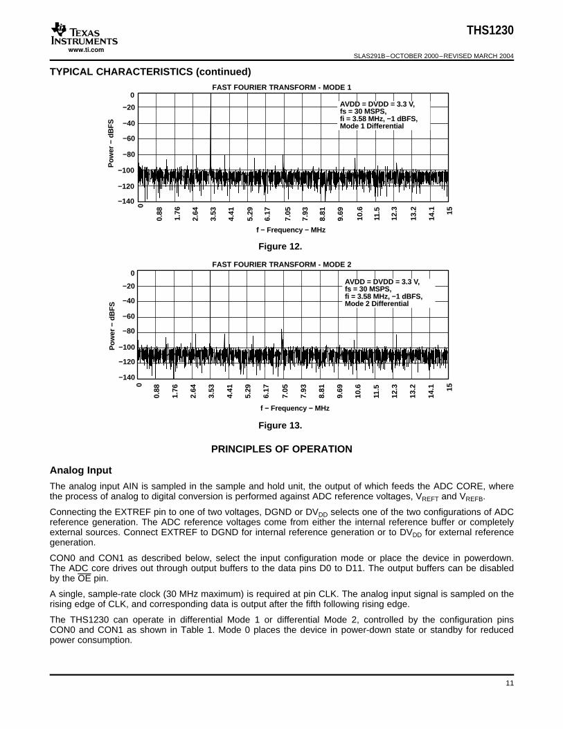
−140
−120
−100
−80
−60
−40
−20
0
0
0.88
1.76
2.64
3.53
4.41
5.29
6.17
7.05
7.93
8.81
9.69
10.6
11.5
12.3
13.2
14.1 15
Po
wer
− d
BF
S
f − Frequency − MHz
AVDD = DVDD = 3.3 V,fs = 30 MSPS,fi = 3.58 MHz, −1 dBFS,Mode 1 Differential
−140
−120
−100
−80
−60
−40
−20
0
0
0.88
1.76
2.64
3.53
4.41
5.29
6.17
7.05
7.93
8.81
9.69
10.6
11.5
12.3
13.2
14.1 15
AVDD = DVDD = 3.3 V,fs = 30 MSPS,fi = 3.58 MHz, −1 dBFS,Mode 2 Differential
Po
wer
− d
BF
S
f − Frequency − MHz
PRINCIPLES OF OPERATION
Analog Input
THS1230
SLAS291B–OCTOBER 2000–REVISED MARCH 2004
TYPICAL CHARACTERISTICS (continued)FAST FOURIER TRANSFORM - MODE 1
Figure 12.
FAST FOURIER TRANSFORM - MODE 2
Figure 13.
The analog input AIN is sampled in the sample and hold unit, the output of which feeds the ADC CORE, wherethe process of analog to digital conversion is performed against ADC reference voltages, VREFT and VREFB.
Connecting the EXTREF pin to one of two voltages, DGND or DVDD selects one of the two configurations of ADCreference generation. The ADC reference voltages come from either the internal reference buffer or completelyexternal sources. Connect EXTREF to DGND for internal reference generation or to DVDD for external referencegeneration.
CON0 and CON1 as described below, select the input configuration mode or place the device in powerdown.The ADC core drives out through output buffers to the data pins D0 to D11. The output buffers can be disabledby the OE pin.
A single, sample-rate clock (30 MHz maximum) is required at pin CLK. The analog input signal is sampled on therising edge of CLK, and corresponding data is output after the fifth following rising edge.
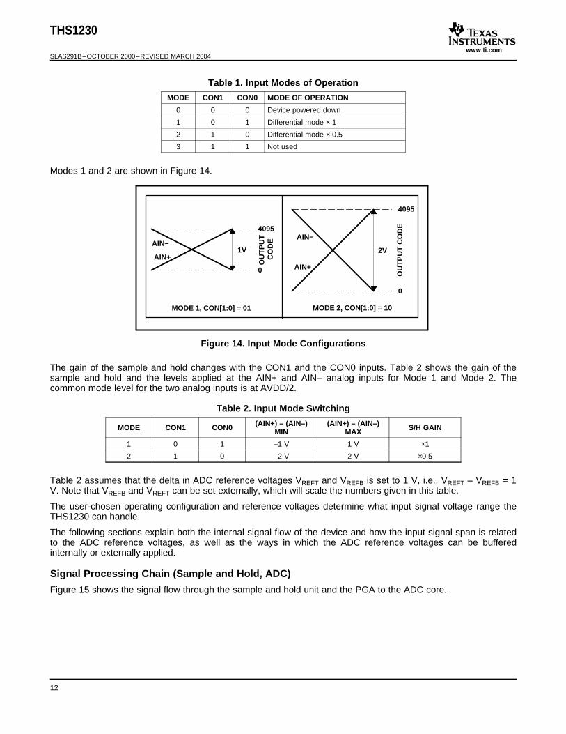
The THS1230 can operate in differential Mode 1 or differential Mode 2, controlled by the configuration pinsCON0 and CON1 as shown in Table 1. Mode 0 places the device in power-down state or standby for reducedpower consumption.
11
www.ti.com
AIN−
0
4095
2V
MODE 2, CON[1:0] = 10
OU
TP
UT
CO
DE
AIN−
0
4095
1V
MODE 1, CON[1:0] = 01
OU
TP
UT
CO
DE
AIN+AIN+
Signal Processing Chain (Sample and Hold, ADC)
THS1230
SLAS291B–OCTOBER 2000–REVISED MARCH 2004
Table 1. Input Modes of Operation
MODE CON1 CON0 MODE OF OPERATION
0 0 0 Device powered down
1 0 1 Differential mode × 1
2 1 0 Differential mode × 0.5
3 1 1 Not used
Modes 1 and 2 are shown in Figure 14.
Figure 14. Input Mode Configurations
The gain of the sample and hold changes with the CON1 and the CON0 inputs. Table 2 shows the gain of thesample and hold and the levels applied at the AIN+ and AIN– analog inputs for Mode 1 and Mode 2. Thecommon mode level for the two analog inputs is at AVDD/2.
Table 2. Input Mode Switching
(AIN+) – (AIN–) (AIN+) – (AIN–)MODE CON1 CON0 S/H GAINMIN MAX
1 0 1 –1 V 1 V ×1
2 1 0 –2 V 2 V ×0.5
Table 2 assumes that the delta in ADC reference voltages VREFT and VREFB is set to 1 V, i.e., VREFT – VREFB = 1V. Note that VREFB and VREFT can be set externally, which will scale the numbers given in this table.
The user-chosen operating configuration and reference voltages determine what input signal voltage range theTHS1230 can handle.
The following sections explain both the internal signal flow of the device and how the input signal span is relatedto the ADC reference voltages, as well as the ways in which the ADC reference voltages can be bufferedinternally or externally applied.
Figure 15 shows the signal flow through the sample and hold unit and the PGA to the ADC core.
12
www.ti.com
SAMPLEAND
HOLDAIN−
AIN+ +1
−1
VP+
VP−
REFT
REFB
ADCCORE
Sample and Hold
Analog-to-Digital Converter
Analog Input
THS1230
RS
VS+ VS−
RS
RSW
RSW
CICI
VCMVCM _
+_+
RS 1
2fCLK CI In(256)–RSW
THS1230
SLAS291B–OCTOBER 2000–REVISED MARCH 2004
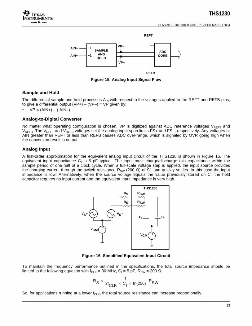
Figure 15. Analog Input Signal Flow
The differential sample and hold processes AIN with respect to the voltages applied to the REFT and REFB pins,to give a differential output (VP+) – (VP–) = VP given by:• VP = (AIN+) – ( AIN–)
No matter what operating configuration is chosen, VP is digitized against ADC reference voltages VREFT andVREFB. The VREFT and VREFB voltages set the analog input span limits FS+ and FS–, respectively. Any voltages atAIN greater than REFT or less than REFB causes ADC over-range, which is signaled by OVR going high whenthe conversion result is output.
A first-order approximation for the equivalent analog input circuit of the THS1230 is shown in Figure 16. Theequivalent input capacitance CI is 5 pF typical. The input must charge/discharge this capacitance within thesample period of one half of a clock cycle. When a full-scale voltage step is applied, the input source providesthe charging current through the switch resistance RSW (200 Ω) of S1 and quickly settles. In this case the inputimpedance is low. Alternatively, when the source voltage equals the value previously stored on CI, the holdcapacitor requires no input current and the equivalent input impedance is very high.
Figure 16. Simplified Equivalent Input Circuit
To maintain the frequency performance outlined in the specifications, the total source impedance should belimited to the following equation with fCLK = 30 MHz, CI = 5 pF, RSW = 200 Ω:
So, for applications running at a lower fCLK, the total source resistance can increase proportionally.
13
www.ti.com
VIN+
VIN−
R1
R2
−
+
R1
R2
−
+
C1
C1
C2
C2
THS1230
AIN+
AIN−
REFT
REFB
AVDD2
THS1230
SLAS291B–OCTOBER 2000–REVISED MARCH 2004
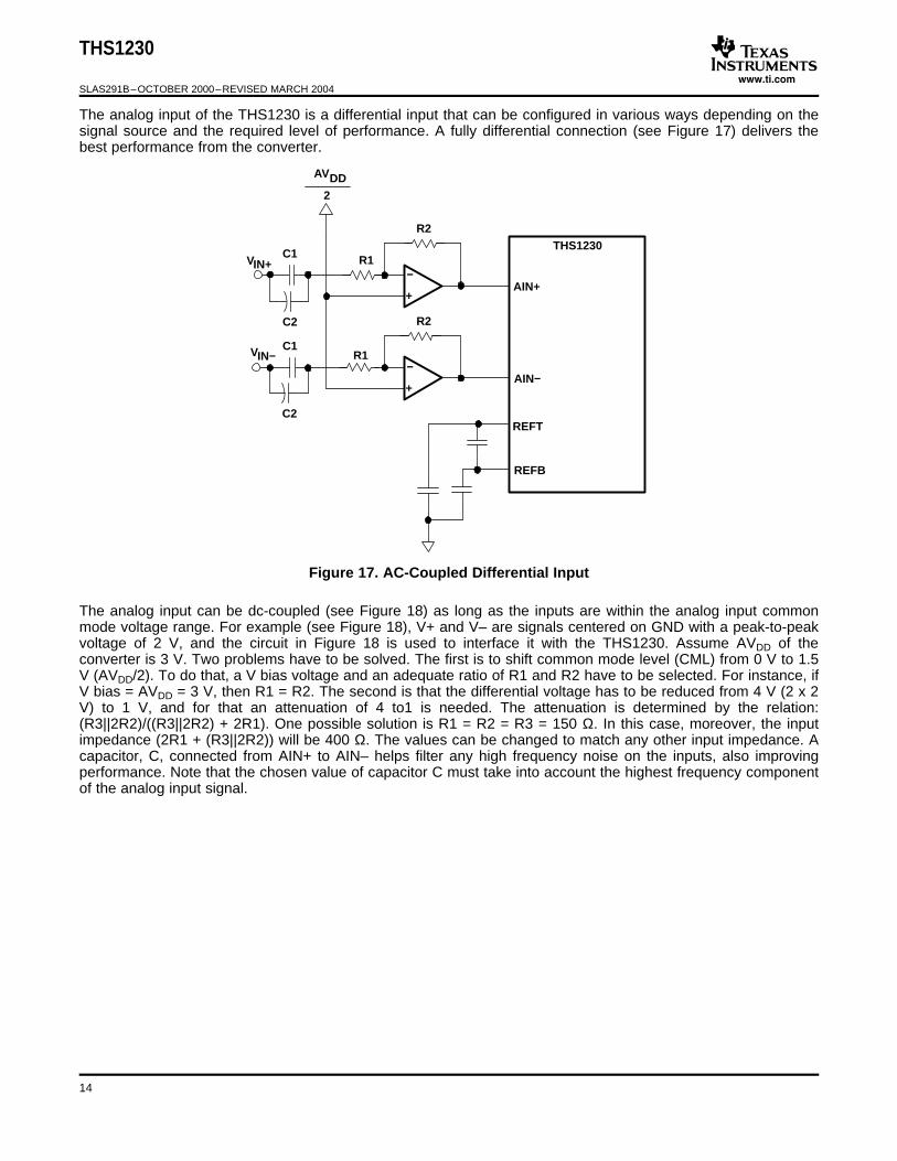
The analog input of the THS1230 is a differential input that can be configured in various ways depending on thesignal source and the required level of performance. A fully differential connection (see Figure 17) delivers thebest performance from the converter.
Figure 17. AC-Coupled Differential Input
The analog input can be dc-coupled (see Figure 18) as long as the inputs are within the analog input commonmode voltage range. For example (see Figure 18), V+ and V– are signals centered on GND with a peak-to-peakvoltage of 2 V, and the circuit in Figure 18 is used to interface it with the THS1230. Assume AVDD of theconverter is 3 V. Two problems have to be solved. The first is to shift common mode level (CML) from 0 V to 1.5V (AVDD/2). To do that, a V bias voltage and an adequate ratio of R1 and R2 have to be selected. For instance, ifV bias = AVDD = 3 V, then R1 = R2. The second is that the differential voltage has to be reduced from 4 V (2 x 2V) to 1 V, and for that an attenuation of 4 to1 is needed. The attenuation is determined by the relation:(R3||2R2)/((R3||2R2) + 2R1). One possible solution is R1 = R2 = R3 = 150 Ω. In this case, moreover, the inputimpedance (2R1 + (R3||2R2)) will be 400 Ω. The values can be changed to match any other input impedance. Acapacitor, C, connected from AIN+ to AIN– helps filter any high frequency noise on the inputs, also improvingperformance. Note that the chosen value of capacitor C must take into account the highest frequency componentof the analog input signal.
14
www.ti.com
VIN+
VIN−
R1
R1
R3
THS1230
AIN+
REFT
REFB
AIN−
R2
R2
VBIAS
VBIAS
V IN
AVDD2
THS1230
AIN+
AIN−
REFT
REFB
Digital Outputs
THS1230
SLAS291B–OCTOBER 2000–REVISED MARCH 2004
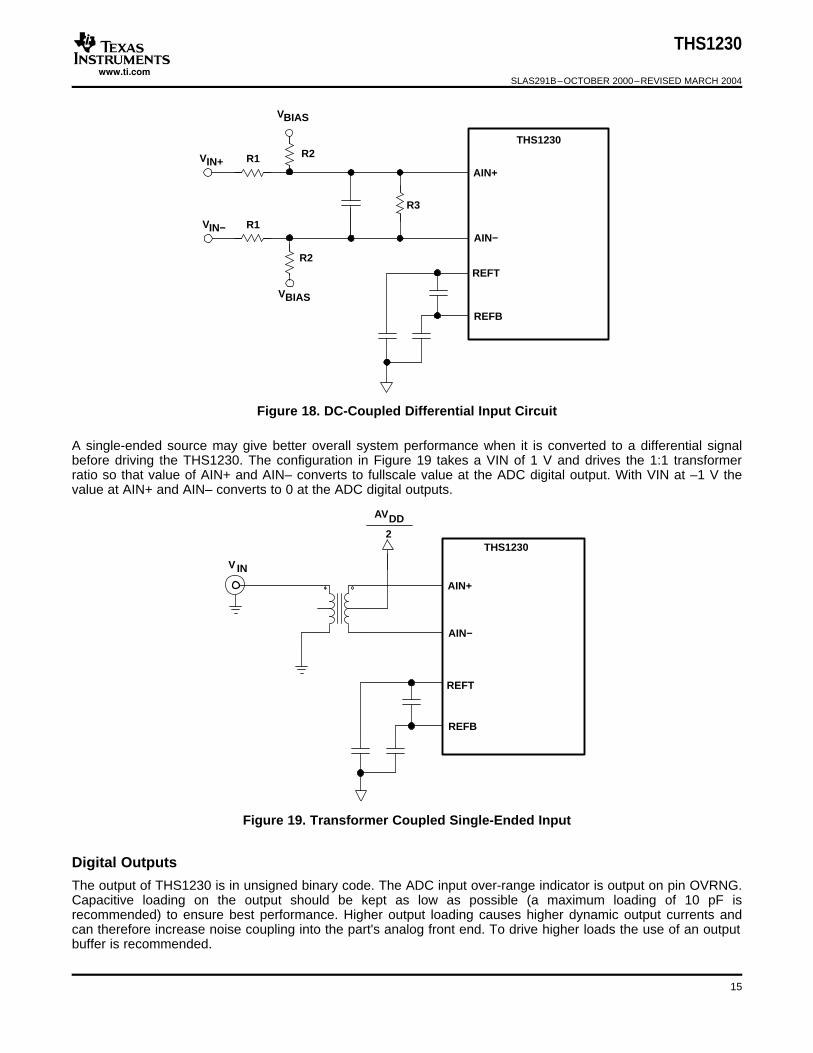
Figure 18. DC-Coupled Differential Input Circuit
A single-ended source may give better overall system performance when it is converted to a differential signalbefore driving the THS1230. The configuration in Figure 19 takes a VIN of 1 V and drives the 1:1 transformerratio so that value of AIN+ and AIN– converts to fullscale value at the ADC digital output. With VIN at –1 V thevalue at AIN+ and AIN– converts to 0 at the ADC digital outputs.
Figure 19. Transformer Coupled Single-Ended Input
The output of THS1230 is in unsigned binary code. The ADC input over-range indicator is output on pin OVRNG.Capacitive loading on the output should be kept as low as possible (a maximum loading of 10 pF isrecommended) to ensure best performance. Higher output loading causes higher dynamic output currents andcan therefore increase noise coupling into the part's analog front end. To drive higher loads the use of an outputbuffer is recommended.
15
www.ti.com
THS1230
DA11
DA0
SN74ALVCH16841
12
1D9
1D0
2D7
2D2
LEOE
1Q9
1Q0
2Q9
2Q2
12
ASICor
DSP
2D1
2D0
2Q1
2Q0
FIFO
D11
D0
1Q15
1Q0 16
DSP
WRTCLK
HF flag INTR
D15
D12
THS1230
DA11
DA0 12
30 MHzClock
CLK
Layout, Decoupling and Grounding Rules
THS1230
SLAS291B–OCTOBER 2000–REVISED MARCH 2004
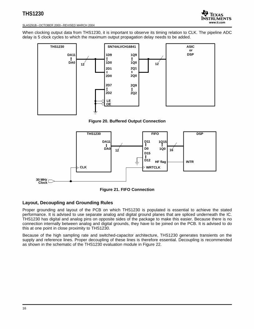
When clocking output data from THS1230, it is important to observe its timing relation to CLK. The pipeline ADCdelay is 5 clock cycles to which the maximum output propagation delay needs to be added.
Figure 20. Buffered Output Connection
Figure 21. FIFO Connection
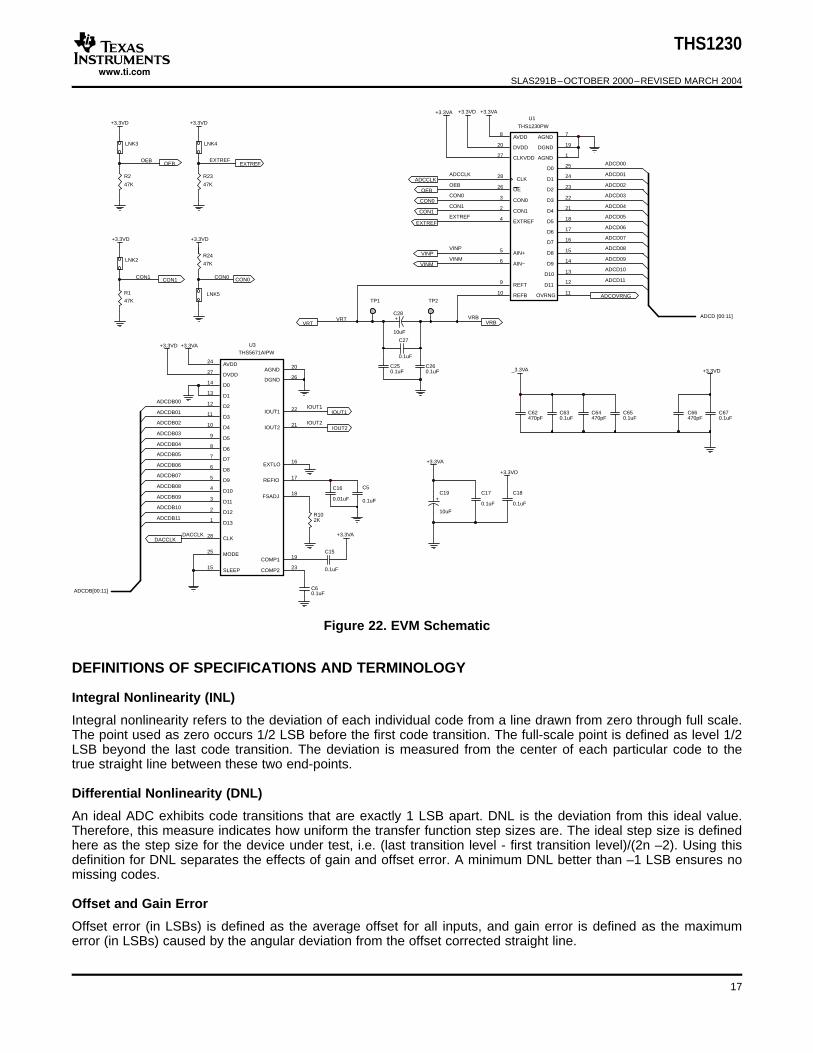
Proper grounding and layout of the PCB on which THS1230 is populated is essential to achieve the statedperformance. It is advised to use separate analog and digital ground planes that are spliced underneath the IC.THS1230 has digital and analog pins on opposite sides of the package to make this easier. Because there is noconnection internally between analog and digital grounds, they have to be joined on the PCB. It is advised to dothis at one point in close proximity to THS1230.
Because of the high sampling rate and switched-capacitor architecture, THS1230 generates transients on thesupply and reference lines. Proper decoupling of these lines is therefore essential. Decoupling is recommendedas shown in the schematic of the THS1230 evaluation module in Figure 22.
16
www.ti.com
AGND 1
CON12
CON03
EXTREF4
AIN+5
AIN−6
AGND 7AVDD8
REFT9
REFB10 OVRNG 11
D11 12
D10 13
D9 14
D8 15
D7 16
D6 17
D5 18
DGND 19DVDD20
D4 21
D3 22
D2 23
D1 24
D0 25
OE26
CLKVDD27
CLK28
U1
THS1230PW
+3.3VA +3.3VD +3.3VA
ADCCLK
OEB
CON0
CON1
EXTREF
VINP
VINM
ADCCLK
OEB
CON0
CON1
EXTREF
VINM
D410
D59
D68
D77
D86
D95
D104
D113
D122
D131
CLK28
MODE25
DVDD27DGND 26AGND 20AVDD24
EXTLO 16
REFIO 17
FSADJ 18
COMP1 19
COMP2 23
IOUT1 22
IOUT2 21
SLEEP15
D311
D212
D113
D014
U3THS5671AIPW
LNK3
LNK2
LNK4
LNK5
R2
47K
R23
47K
R1
47K
R24
47K
+3.3VD +3.3VD
+3.3VD +3.3VD
OEB EXTREF
CON1 CON0 CON0
TP1 TP2
+
C28
10uF
C27
0.1uF
C250.1uF
C260.1uF
VRT VRBVRT VRB
C62470pF
C630.1uF
C64470pF
C650.1uF
C66470pF
C670.1uF
+3.3VD_3.3VA
ADCOVRNG
ADCD00
ADCD01
ADCD02
ADCD03
ADCD04
ADCD05
ADCD06
ADCD07
ADCD08
ADCD09
ADCD10
ADCD11
ADCD [00:11]
+3.3VA+3.3VD
ADCDB00
ADCDB01
ADCDB02
ADCDB03
ADCDB04
ADCDB05
ADCDB06
ADCDB07
ADCDB08
ADCDB09
ADCDB10
ADCDB11
ADCDB[00:11]
DACCLKDACCLK
C60.1uF
C15
0.1uF
+3.3VA
IOUT1
IOUT2
R102K
C16
0.01uF
C5
0.1uF
C19
10uF
C17
0.1uF
C18
0.1uF
+3.3VD
+3.3VA
CON1
OEB EXTREF
IOUT1
IOUT2
+
VINP
DEFINITIONS OF SPECIFICATIONS AND TERMINOLOGY
Integral Nonlinearity (INL)
Differential Nonlinearity (DNL)
Offset and Gain Error
THS1230
SLAS291B–OCTOBER 2000–REVISED MARCH 2004
Figure 22. EVM Schematic
Integral nonlinearity refers to the deviation of each individual code from a line drawn from zero through full scale.The point used as zero occurs 1/2 LSB before the first code transition. The full-scale point is defined as level 1/2LSB beyond the last code transition. The deviation is measured from the center of each particular code to thetrue straight line between these two end-points.
An ideal ADC exhibits code transitions that are exactly 1 LSB apart. DNL is the deviation from this ideal value.Therefore, this measure indicates how uniform the transfer function step sizes are. The ideal step size is definedhere as the step size for the device under test, i.e. (last transition level - first transition level)/(2n –2). Using thisdefinition for DNL separates the effects of gain and offset error. A minimum DNL better than –1 LSB ensures nomissing codes.
Offset error (in LSBs) is defined as the average offset for all inputs, and gain error is defined as the maximumerror (in LSBs) caused by the angular deviation from the offset corrected straight line.
17

www.ti.com
Analog Input Bandwidth
Output Timing
Signal-to-Noise Ratio + Distortion (SINAD)
Effective Number of Bits (ENOB)
Total Harmonic Distortion (THD)
Spurious Free Dynamic Range (SFDR)
THS1230
SLAS291B–OCTOBER 2000–REVISED MARCH 2004
The analog input bandwidth is defined as the maximum frequency of a 1-dBFS input sine wave that can beapplied to the device for which an extra 3-dB attenuation is observed in the reconstructed output signal.
Output timing td(O) is measured from the 50% level of the CLK input falling edge to the 10%/90% level of thedigital output. The digital output load is not higher than 10 pF.
Output hold time th(O) is measured from the 50% level of the CLK input falling edge to the10%/90% level of thedigital output. The digital output load is not less than 2 pF.
Aperture delay td(A) is measured from the 50% level of the CLK input to the actual sampling instant.
The OE signal is asynchronous.
OE timing td(PZ) is measured from the VIH(min) level of OE to the high-impedance state of the output data. Thedigital output load is not higher than 10 pF.
OE timing td(EN) is measured from the VIL(max) level of OE to the instant when the output data reaches VOH(min) orVOL(max) output levels. The digital output load is not higher than 10 pF.
SINAD is the ratio of the rms value of the measured input signal to the rms sum of all other spectral componentsbelow the Nyquist frequency, including harmonics but excluding dc. The value for SINAD is expressed indecibels.
For a sine wave, SINAD can be expressed in terms of the number of bits. Using the following formula,• N = (SINAD – 1.76)/6.02
it is possible to get a measure of performance expressed as N, the effective number of bits. Thus, effectivenumber of bits for a device for sine wave inputs at a given input frequency can be calculated directly from itsmeasured SINAD.
THD is the ratio of the rms sum of the first six harmonic components to the rms value of the measured inputsignal and is expressed as a percentage or in decibels.
SFDR is the difference in dB between the rms amplitude of the input signal and the peak spurious signal.
18

PACKAGING INFORMATION
Orderable Device Status (1) PackageType
PackageDrawing
Pins PackageQty
Eco Plan (2) Lead/Ball Finish MSL Peak Temp (3)
THS1230CDW ACTIVE SOIC DW 28 20 Green (RoHS &no Sb/Br)
CU NIPDAU Level-1-260C-UNLIM
THS1230CDWG4 ACTIVE SOIC DW 28 20 Green (RoHS &no Sb/Br)
CU NIPDAU Level-1-260C-UNLIM
THS1230CDWRG4 ACTIVE SOIC DW 28 TBD Call TI Call TI
THS1230CPW ACTIVE TSSOP PW 28 50 Green (RoHS &no Sb/Br)
CU NIPDAU Level-1-260C-UNLIM
THS1230CPWG4 ACTIVE TSSOP PW 28 50 Green (RoHS &no Sb/Br)
CU NIPDAU Level-1-260C-UNLIM
THS1230CPWRG4 ACTIVE TSSOP PW 28 TBD Call TI Call TI
THS1230IDW ACTIVE SOIC DW 28 20 Green (RoHS &no Sb/Br)
CU NIPDAU Level-1-260C-UNLIM
THS1230IDWG4 ACTIVE SOIC DW 28 20 Green (RoHS &no Sb/Br)
CU NIPDAU Level-1-260C-UNLIM
THS1230IDWRG4 ACTIVE SOIC DW 28 TBD Call TI Call TI
THS1230IPW ACTIVE TSSOP PW 28 50 Green (RoHS &no Sb/Br)
CU NIPDAU Level-1-260C-UNLIM
THS1230IPWG4 ACTIVE TSSOP PW 28 50 Green (RoHS &no Sb/Br)
CU NIPDAU Level-1-260C-UNLIM
THS1230IPWR ACTIVE TSSOP PW 28 2000 Green (RoHS &no Sb/Br)
CU NIPDAU Level-1-260C-UNLIM
THS1230IPWRG4 ACTIVE TSSOP PW 28 2000 Green (RoHS &no Sb/Br)
CU NIPDAU Level-1-260C-UNLIM
(1) The marketing status values are defined as follows:ACTIVE: Product device recommended for new designs.LIFEBUY: TI has announced that the device will be discontinued, and a lifetime-buy period is in effect.NRND: Not recommended for new designs. Device is in production to support existing customers, but TI does not recommend using this part ina new design.PREVIEW: Device has been announced but is not in production. Samples may or may not be available.OBSOLETE: TI has discontinued the production of the device.
(2) Eco Plan - The planned eco-friendly classification: Pb-Free (RoHS), Pb-Free (RoHS Exempt), or Green (RoHS & no Sb/Br) - please checkhttp://www.ti.com/productcontent for the latest availability information and additional product content details.TBD: The Pb-Free/Green conversion plan has not been defined.Pb-Free (RoHS): TI's terms "Lead-Free" or "Pb-Free" mean semiconductor products that are compatible with the current RoHS requirementsfor all 6 substances, including the requirement that lead not exceed 0.1% by weight in homogeneous materials. Where designed to be solderedat high temperatures, TI Pb-Free products are suitable for use in specified lead-free processes.Pb-Free (RoHS Exempt): This component has a RoHS exemption for either 1) lead-based flip-chip solder bumps used between the die andpackage, or 2) lead-based die adhesive used between the die and leadframe. The component is otherwise considered Pb-Free (RoHScompatible) as defined above.Green (RoHS & no Sb/Br): TI defines "Green" to mean Pb-Free (RoHS compatible), and free of Bromine (Br) and Antimony (Sb) based flameretardants (Br or Sb do not exceed 0.1% by weight in homogeneous material)
(3) MSL, Peak Temp. -- The Moisture Sensitivity Level rating according to the JEDEC industry standard classifications, and peak soldertemperature.
Important Information and Disclaimer:The information provided on this page represents TI's knowledge and belief as of the date that it isprovided. TI bases its knowledge and belief on information provided by third parties, and makes no representation or warranty as to theaccuracy of such information. Efforts are underway to better integrate information from third parties. TI has taken and continues to takereasonable steps to provide representative and accurate information but may not have conducted destructive testing or chemical analysis onincoming materials and chemicals. TI and TI suppliers consider certain information to be proprietary, and thus CAS numbers and other limitedinformation may not be available for release.
PACKAGE OPTION ADDENDUM
www.ti.com 19-Jun-2007
Addendum-Page 1
In no event shall TI's liability arising out of such information exceed the total purchase price of the TI part(s) at issue in this document sold by TIto Customer on an annual basis.
PACKAGE OPTION ADDENDUM
www.ti.com 19-Jun-2007
Addendum-Page 2
MECHANICAL DATA
MTSS001C – JANUARY 1995 – REVISED FEBRUARY 1999
POST OFFICE BOX 655303 • DALLAS, TEXAS 75265
PW (R-PDSO-G**) PLASTIC SMALL-OUTLINE PACKAGE14 PINS SHOWN
0,65 M0,10
0,10
0,25
0,500,75
0,15 NOM
Gage Plane
28
9,80
9,60
24
7,90
7,70
2016
6,60
6,40
4040064/F 01/97
0,30
6,606,20
8
0,19
4,304,50
7
0,15
14
A
1
1,20 MAX
14
5,10
4,90
8
3,10
2,90
A MAX
A MIN
DIMPINS **
0,05
4,90
5,10
Seating Plane
0°–8°
NOTES: A. All linear dimensions are in millimeters.B. This drawing is subject to change without notice.C. Body dimensions do not include mold flash or protrusion not to exceed 0,15.D. Falls within JEDEC MO-153

IMPORTANT NOTICE
Texas Instruments Incorporated and its subsidiaries (TI) reserve the right to make corrections, modifications, enhancements,improvements, and other changes to its products and services at any time and to discontinue any product or service without notice.Customers should obtain the latest relevant information before placing orders and should verify that such information is current andcomplete. All products are sold subject to TI’s terms and conditions of sale supplied at the time of order acknowledgment.
TI warrants performance of its hardware products to the specifications applicable at the time of sale in accordance with TI’sstandard warranty. Testing and other quality control techniques are used to the extent TI deems necessary to support thiswarranty. Except where mandated by government requirements, testing of all parameters of each product is not necessarilyperformed.
TI assumes no liability for applications assistance or customer product design. Customers are responsible for their products andapplications using TI components. To minimize the risks associated with customer products and applications, customers shouldprovide adequate design and operating safeguards.
TI does not warrant or represent that any license, either express or implied, is granted under any TI patent right, copyright, maskwork right, or other TI intellectual property right relating to any combination, machine, or process in which TI products or servicesare used. Information published by TI regarding third-party products or services does not constitute a license from TI to use suchproducts or services or a warranty or endorsement thereof. Use of such information may require a license from a third party underthe patents or other intellectual property of the third party, or a license from TI under the patents or other intellectual property of TI.
Reproduction of TI information in TI data books or data sheets is permissible only if reproduction is without alteration and isaccompanied by all associated warranties, conditions, limitations, and notices. Reproduction of this information with alteration is anunfair and deceptive business practice. TI is not responsible or liable for such altered documentation. Information of third partiesmay be subject to additional restrictions.
Resale of TI products or services with statements different from or beyond the parameters stated by TI for that product or servicevoids all express and any implied warranties for the associated TI product or service and is an unfair and deceptive businesspractice. TI is not responsible or liable for any such statements.
TI products are not authorized for use in safety-critical applications (such as life support) where a failure of the TI product wouldreasonably be expected to cause severe personal injury or death, unless officers of the parties have executed an agreementspecifically governing such use. Buyers represent that they have all necessary expertise in the safety and regulatory ramificationsof their applications, and acknowledge and agree that they are solely responsible for all legal, regulatory and safety-relatedrequirements concerning their products and any use of TI products in such safety-critical applications, notwithstanding anyapplications-related information or support that may be provided by TI. Further, Buyers must fully indemnify TI and itsrepresentatives against any damages arising out of the use of TI products in such safety-critical applications.
TI products are neither designed nor intended for use in military/aerospace applications or environments unless the TI products arespecifically designated by TI as military-grade or "enhanced plastic." Only products designated by TI as military-grade meet militaryspecifications. Buyers acknowledge and agree that any such use of TI products which TI has not designated as military-grade issolely at the Buyer's risk, and that they are solely responsible for compliance with all legal and regulatory requirements inconnection with such use.
TI products are neither designed nor intended for use in automotive applications or environments unless the specific TI productsare designated by TI as compliant with ISO/TS 16949 requirements. Buyers acknowledge and agree that, if they use anynon-designated products in automotive applications, TI will not be responsible for any failure to meet such requirements.
Following are URLs where you can obtain information on other Texas Instruments products and application solutions:
Products Applications
Amplifiers amplifier.ti.com Audio www.ti.com/audio
Data Converters dataconverter.ti.com Automotive www.ti.com/automotive
DSP dsp.ti.com Broadband www.ti.com/broadband
Interface interface.ti.com Digital Control www.ti.com/digitalcontrol
Logic logic.ti.com Military www.ti.com/military
Power Mgmt power.ti.com Optical Networking www.ti.com/opticalnetwork
Microcontrollers microcontroller.ti.com Security www.ti.com/security
RFID www.ti-rfid.com Telephony www.ti.com/telephony
Low Power www.ti.com/lpw Video & Imaging www.ti.com/videoWireless
Wireless www.ti.com/wireless
Mailing Address: Texas Instruments, Post Office Box 655303, Dallas, Texas 75265Copyright © 2007, Texas Instruments Incorporated