Embed Size (px)
Citation preview
2021 Microchip Technology Inc. and its subsidiaries DS20006622A-page 1
SY88343BL
Features• Single 3.3V Power Supply• DC to 3.2 Gbps Operation• Low-Noise CML Data Outputs• High Gain LOS• Chatter-Free Open-Collector TTL Loss-of-Signal
(LOS) Output with Internal 4.75 kΩ Pull-Up Resistor
• TTL /EN Input• Programmable LOS Level Set (LOSLVL)• Ideal for Multi-Rate Applications• Available in a 16-Lead VQFN Package
Applications• APON, BPON, EPON, and GPON• Gigabit Ethernet• Fibre Channel• OC-3 and OC-12/24 SONET/SDH• High-Gain Line Driver and Line Receiver
Markets• FTTP• Optical Transceivers• Datacom/Telecom• Low-Gain TIA Interface• Long-Reach FOM
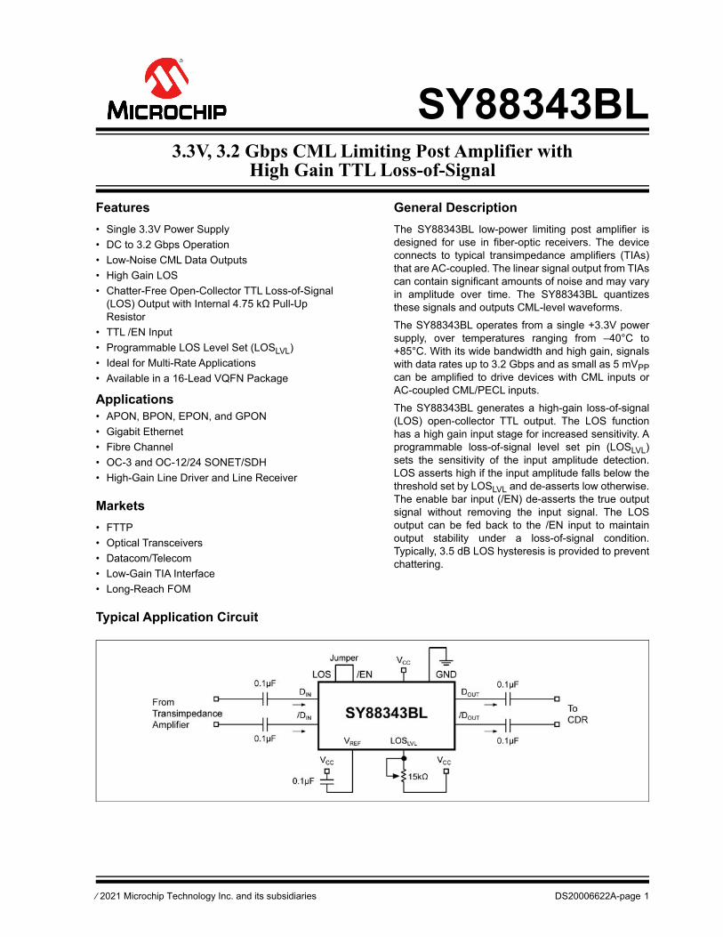
General DescriptionThe SY88343BL low-power limiting post amplifier isdesigned for use in fiber-optic receivers. The deviceconnects to typical transimpedance amplifiers (TIAs)that are AC-coupled. The linear signal output from TIAscan contain significant amounts of noise and may varyin amplitude over time. The SY88343BL quantizesthese signals and outputs CML-level waveforms.The SY88343BL operates from a single +3.3V powersupply, over temperatures ranging from –40°C to+85°C. With its wide bandwidth and high gain, signalswith data rates up to 3.2 Gbps and as small as 5 mVPPcan be amplified to drive devices with CML inputs orAC-coupled CML/PECL inputs.The SY88343BL generates a high-gain loss-of-signal(LOS) open-collector TTL output. The LOS functionhas a high gain input stage for increased sensitivity. Aprogrammable loss-of-signal level set pin (LOSLVL)sets the sensitivity of the input amplitude detection.LOS asserts high if the input amplitude falls below thethreshold set by LOSLVL and de-asserts low otherwise.The enable bar input (/EN) de-asserts the true outputsignal without removing the input signal. The LOSoutput can be fed back to the /EN input to maintainoutput stability under a loss-of-signal condition.Typically, 3.5 dB LOS hysteresis is provided to preventchattering.
Typical Application Circuit
3.3V, 3.2 Gbps CML Limiting Post Amplifier withHigh Gain TTL Loss-of-Signal
SY88343BL
DS20006622A-page 2 2021 Microchip Technology Inc. and its subsidiaries
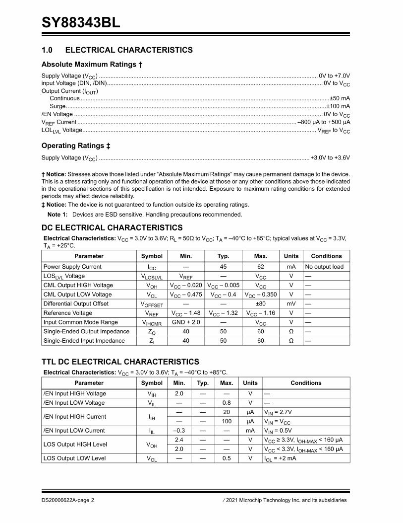
1.0 ELECTRICAL CHARACTERISTICSAbsolute Maximum Ratings †Supply Voltage (VCC) ..................................................................................................................................... 0V to +7.0Vinput Voltage (DIN, /DIN)................................................................................................................................... 0V to VCCOutput Current (IOUT) Continuous .......................................................................................................................................................±50 mA Surge..............................................................................................................................................................±100 mA/EN Voltage ....................................................................................................................................................... 0V to VCCVREF Current ..................................................................................................................................... –800 µA to +500 µALOLLVL Voltage.............................................................................................................................................. VREF to VCC
Operating Ratings ‡Supply Voltage (VCC) ................................................................................................................................ +3.0V to +3.6V
† Notice: Stresses above those listed under “Absolute Maximum Ratings” may cause permanent damage to the device.This is a stress rating only and functional operation of the device at those or any other conditions above those indicatedin the operational sections of this specification is not intended. Exposure to maximum rating conditions for extendedperiods may affect device reliability.‡ Notice: The device is not guaranteed to function outside its operating ratings.
Note 1: Devices are ESD sensitive. Handling precautions recommended.
DC ELECTRICAL CHARACTERISTICSElectrical Characteristics: VCC = 3.0V to 3.6V; RL = 50Ω to VCC; TA = –40°C to +85°C; typical values at VCC = 3.3V, TA = +25°C.
Parameter Symbol Min. Typ. Max. Units ConditionsPower Supply Current ICC — 45 62 mA No output loadLOSLVL Voltage VLOSLVL VREF — VCC V —CML Output HIGH Voltage VOH VCC – 0.020 VCC – 0.005 VCC V —CML Output LOW Voltage VOL VCC – 0.475 VCC – 0.4 VCC – 0.350 V —Differential Output Offset VOFFSET — — ±80 mV —Reference Voltage VREF VCC – 1.48 VCC – 1.32 VCC – 1.16 V —Input Common Mode Range VIHCMR GND + 2.0 — VCC V —Single-Ended Output Impedance ZO 40 50 60 Ω —Single-Ended Input Impedance ZI 40 50 60 Ω —
TTL DC ELECTRICAL CHARACTERISTICSElectrical Characteristics: VCC = 3.0V to 3.6V; TA = –40°C to +85°C.
Parameter Symbol Min. Typ. Max. Units Conditions/EN Input HIGH Voltage VIH 2.0 — — V —/EN Input LOW Voltage VIL — — 0.8 V —
/EN Input HIGH Current IIH— — 20 µA VIN = 2.7V— — 100 µA VIN = VCC
/EN Input LOW Current IIL –0.3 — — mA VIN = 0.5V
LOS Output HIGH Level VOH2.4 — — V VCC ≥ 3.3V, IOH-MAX < 160 μA2.0 — — V VCC < 3.3V, IOH-MAX < 160 μA
LOS Output LOW Level VOL — — 0.5 V IOL = +2 mA
2021 Microchip Technology Inc. and its subsidiaries DS20006622A-page 3
SY88343BL
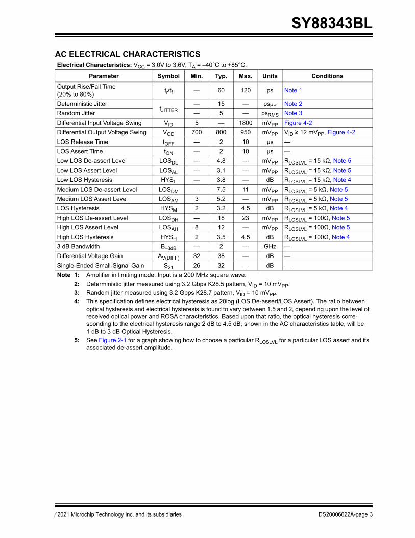
AC ELECTRICAL CHARACTERISTICSElectrical Characteristics: VCC = 3.0V to 3.6V; TA = –40°C to +85°C.
Parameter Symbol Min. Typ. Max. Units ConditionsOutput Rise/Fall Time(20% to 80%) tr/tf — 60 120 ps Note 1
Deterministic JittertJITTER
— 15 — psPP Note 2Random Jitter — 5 — psRMS Note 3Differential Input Voltage Swing VID 5 — 1800 mVPP Figure 4-2Differential Output Voltage Swing VOD 700 800 950 mVPP VID ≥ 12 mVPP, Figure 4-2LOS Release Time tOFF — 2 10 µs —LOS Assert Time tON — 2 10 µs —Low LOS De-assert Level LOSDL — 4.8 — mVPP RLOSLVL = 15 kΩ, Note 5Low LOS Assert Level LOSAL — 3.1 — mVPP RLOSLVL = 15 kΩ, Note 5Low LOS Hysteresis HYSL — 3.8 — dB RLOSLVL = 15 kΩ, Note 4Medium LOS De-assert Level LOSDM — 7.5 11 mVPP RLOSLVL = 5 kΩ, Note 5Medium LOS Assert Level LOSAM 3 5.2 — mVPP RLOSLVL = 5 kΩ, Note 5LOS Hysteresis HYSM 2 3.2 4.5 dB RLOSLVL = 5 kΩ, Note 4High LOS De-assert Level LOSDH — 18 23 mVPP RLOSLVL = 100Ω, Note 5High LOS Assert Level LOSAH 8 12 — mVPP RLOSLVL = 100Ω, Note 5High LOS Hysteresis HYSH 2 3.5 4.5 dB RLOSLVL = 100Ω, Note 43 dB Bandwidth B–3dB — 2 — GHz —Differential Voltage Gain AV(DIFF) 32 38 — dB —Single-Ended Small-Signal Gain S21 26 32 — dB —Note 1: Amplifier in limiting mode. Input is a 200 MHz square wave.
2: Deterministic jitter measured using 3.2 Gbps K28.5 pattern, VID = 10 mVPP.3: Random jitter measured using 3.2 Gbps K28.7 pattern, VID = 10 mVPP.4: This specification defines electrical hysteresis as 20log (LOS De-assert/LOS Assert). The ratio between
optical hysteresis and electrical hysteresis is found to vary between 1.5 and 2, depending upon the level of received optical power and ROSA characteristics. Based upon that ratio, the optical hysteresis corre-sponding to the electrical hysteresis range 2 dB to 4.5 dB, shown in the AC characteristics table, will be 1 dB to 3 dB Optical Hysteresis.
5: See Figure 2-1 for a graph showing how to choose a particular RLOSLVL for a particular LOS assert and its associated de-assert amplitude.

SY88343BL
DS20006622A-page 4 2021 Microchip Technology Inc. and its subsidiaries
TEMPERATURE SPECIFICATIONS (Note 1)Parameters Sym. Min. Typ. Max. Units Conditions
Temperature RangesAmbient Temperature TA –40 — +85 °C —Lead Temperature — — — +260 °C Soldering, 10 sec.Storage Temperature TS –65 — +150 °C —Package Thermal ResistanceThermal Resistance, VQFN 16-Ld, Note 2
θJA — 61 — °C/W —ψJB — 38 — °C/W —
Note 1: The maximum allowable power dissipation is a function of ambient temperature, the maximum allowable junction temperature and the thermal resistance from junction to air (i.e., TA, TJ, JA). Exceeding the maximum allowable power dissipation will cause the device operating junction temperature to exceed the maximum +85°C rating. Sustained junction temperatures above +85°C can impact the device reliability.
2: Thermal performance assumes the use of a 4-layer PCB. Exposed pad must be soldered (or equivalent) to the device’s most negative potential on the PCB.

2021 Microchip Technology Inc. and its subsidiaries DS20006622A-page 5
SY88343BL2.0 TYPICAL PERFORMANCE CURVES
FIGURE 2-1: VID to Assert/De-Assert LOS vs. RLOSLVL.
FIGURE 2-2: LOS Hysteresis vs. RLOSLVL.
Note: The graphs and tables provided following this note are a statistical summary based on a limited number ofsamples and are provided for informational purposes only. The performance characteristics listed hereinare not tested or guaranteed. In some graphs or tables, the data presented may be outside the specifiedoperating range (e.g., outside specified power supply range) and therefore outside the warranted range.
RLOSLVL (kΩ)
RLOSLVL (k
SY88343BL
DS20006622A-page 6 2021 Microchip Technology Inc. and its subsidiaries
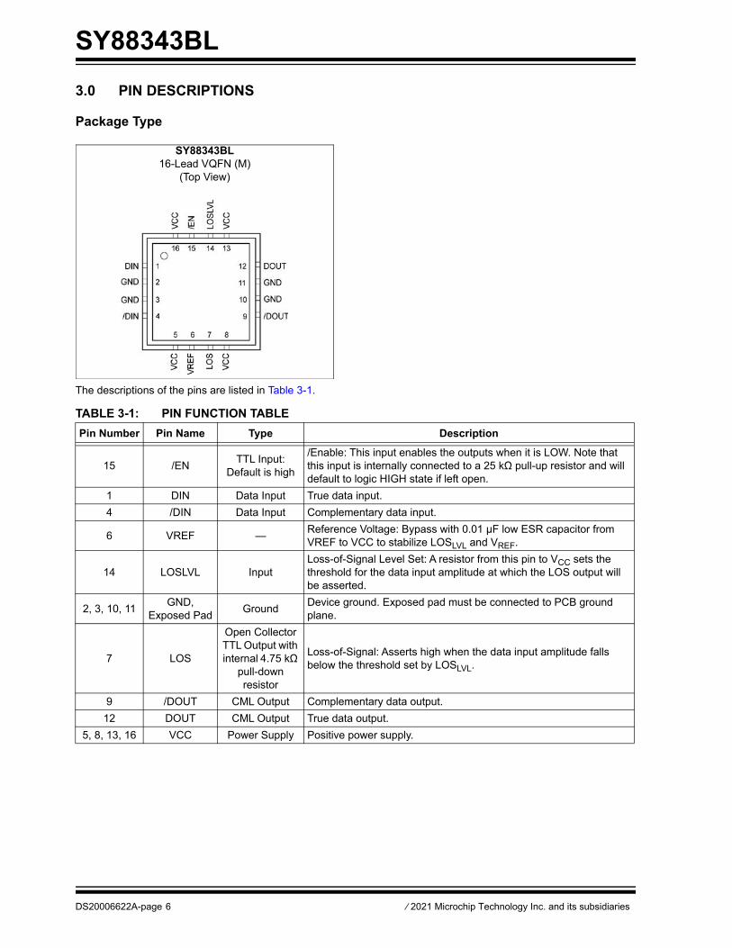
3.0 PIN DESCRIPTIONS
Package Type
The descriptions of the pins are listed in Table 3-1.
SY88343BL16-Lead VQFN (M)
(Top View)
TABLE 3-1: PIN FUNCTION TABLEPin Number Pin Name Type Description
15 /EN TTL Input: Default is high
/Enable: This input enables the outputs when it is LOW. Note that this input is internally connected to a 25 kΩ pull-up resistor and will default to logic HIGH state if left open.
1 DIN Data Input True data input.4 /DIN Data Input Complementary data input.
6 VREF — Reference Voltage: Bypass with 0.01 μF low ESR capacitor from VREF to VCC to stabilize LOSLVL and VREF.
14 LOSLVL InputLoss-of-Signal Level Set: A resistor from this pin to VCC sets the threshold for the data input amplitude at which the LOS output will be asserted.
2, 3, 10, 11 GND,Exposed Pad Ground Device ground. Exposed pad must be connected to PCB ground
plane.
7 LOS
Open Collector TTL Output with internal 4.75 kΩ
pull-down resistor
Loss-of-Signal: Asserts high when the data input amplitude falls below the threshold set by LOSLVL.
9 /DOUT CML Output Complementary data output.12 DOUT CML Output True data output.
5, 8, 13, 16 VCC Power Supply Positive power supply.

2021 Microchip Technology Inc. and its subsidiaries DS20006622A-page 7
SY88343BL4.0 FUNCTIONAL DESCRIPTION
Functional Block Diagram
The SY88343BL low-power limiting post amplifieroperates from a single +3.3V power supply, overtemperatures from –40°C to +85°C. Signals with datarates up to 3.2 Gbps and as small as 5 mVPP can beamplified. Figure 4-1 shows the allowed input voltageswing. The SY88343BL generates a LOS outputallowing feedback to /EN for output stability. LOSLVLsets the sensitivity of the input amplitude detection.
4.1 Input Amplifier BufferFigure 4-2 shows a simplified schematic of the inputstage. The high-sensitivity of the input amplifier allowssignals as small as 5 mVPP to be detected andamplified. The input amplifier also allows input signalsas large as 1800 mVPP. Input signals are linearlyamplified with a typical 38 dB differential voltage gain.Because it is a limiting amplifier, this device outputstypically 800 mVPP voltage-limited waveforms for inputsignals greater than 12 mVPP. Applications that requirethe SY88343BL to operate with high gain should havethe upstream TIA placed as close as possible to thedevice’s input pins. This ensures the best performanceof the device.
4.2 Output BufferThe SY88343BL’s CML output buffer is designed todrive 50Ω lines. The output buffer requires appropriatetermination for proper operation. An external 50Ωresistor to VCC for each output pin provides this.Figure 4-4 shows a simplified schematic of the outputstage.
4.3 Loss-of-SignalThe SY88343BL generates a chatter-free LOSopen-collector TTL output with an internal 4.75 kΩpull-up resistor, as shown in Figure 4-3. LOS is used todetermine that the input amplitude is large enough tobe considered a valid input. LOS asserts high if theinput amplitude falls below the threshold sets byLOSLVL and de-asserts low otherwise. LOS can be fedback to the enable bar (/EN) input to maintain outputstability under a loss-of-signal condition. /ENde-asserts the true output signal without removing theinput signals. Typical, 3.5 dB LOS hysteresis isprovided to prevent chattering.
4.4 Loss-of-Signal Level SetProgrammable LOS level-set pin (LOSLVL) sets thethreshold of the input amplitude detection. Connectingan external resistor between VCC and LOSLVL sets thevoltage at LOSLVL. This voltage ranges from VCC toVREF. The external resistor creates a voltage dividerbetween VCC and VREF, as shown in Figure 4-5.
4.5 HysteresisThe SY88343BL provides typically 3.5 dB LOSelectrical hysteresis. By definition, a power ratiomeasured in dB is 10log (power ratio). Power iscalculated as VIN
2/R for an electrical signal. Hence, thesame ratio can be stated as 20log (voltage ratio). Whilein linear mode, the electrical voltage input changeslinearly with the optical power and therefore, the ratioschange linearly. Thus, the optical hysteresis in dB ishalf the electrical hysteresis in dB given in the datasheet. Because the SY88343BL is an electrical device,this data sheet refers to hysteresis in electrical terms.With 3.5 dB LOS hysteresis, a voltage factor of 1.5 isrequired to assert or de-assert LOS.

SY88343BL
DS20006622A-page 8 2021 Microchip Technology Inc. and its subsidiaries
FIGURE 4-1: VIS and VID.
FIGURE 4-2: Input Structure.
FIGURE 4-3: LOS Output Structure.
FIGURE 4-4: Output Structure.
FIGURE 4-5: LOSLVL Setting Circuit.

2021 Microchip Technology Inc. and its subsidiaries DS20006622A-page 9
SY88343BL5.0 PACKAGING INFORMATION
5.1 Package Marking Information
Example16-Lead VQFN*
–XXXXWNNN
–343B5354
Legend: XX...X Product code or customer-specific informationY Year code (last digit of calendar year)YY Year code (last 2 digits of calendar year)WW Week code (week of January 1 is week ‘01’)NNN Alphanumeric traceability code Pb-free JEDEC® designator for Matte Tin (Sn)* This package is Pb-free. The Pb-free JEDEC designator ( )
can be found on the outer packaging for this package.●, ▲, ▼ Pin one index is identified by a dot, delta up, or delta down (trianglemark).
Note: In the event the full Microchip part number cannot be marked on one line, it willbe carried over to the next line, thus limiting the number of availablecharacters for customer-specific information. Package may or may not includethe corporate logo.Underbar (_) and/or Overbar (‾) symbol may not be to scale.
3e
3e
SY88343BL
DS20006622A-page 10 2021 Microchip Technology Inc. and its subsidiaries
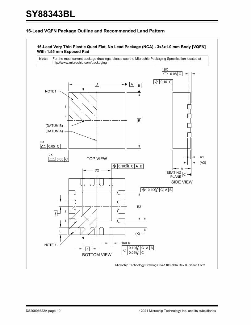
16-Lead VQFN Package Outline and Recommended Land Pattern
BA
0.05 C
0.05 C
0.10 C A B0.05 C
C
2XTOP VIEW
SIDE VIEW
BOTTOM VIEW
1
2
N
0.10 C A B
0.10 C A B
0.10 C
0.08 C
Sheet 1 of 2
2X
16X
For the most current package drawings, please see the Microchip Packaging Specification located athttp://www.microchip.com/packaging
16-Lead Very Thin Plastic Quad Flat, No Lead Package (NCA) - 3x3x1.0 mm Body [VQFN]With 1.55 mm Exposed Pad
Note:
Microchip Technology Drawing C04-1103-NCA Rev B
NOTE1
(DATUM B)(DATUM A)
NOTE 1
SEATINGPLANE
A1(A3)
A
D
E
D2
E2
(K)
16X b
e
e2
L
1
2
N

2021 Microchip Technology Inc. and its subsidiaries DS20006622A-page 11
SY88343BL
For the most current package drawings, please see the Microchip Packaging Specification located athttp://www.microchip.com/packaging
Note:
REF: Reference Dimension, usually without tolerance, for information purposes only.BSC: Basic Dimension. Theoretically exact value shown without tolerances.
Notes:
1.2.3.
Pin 1 visual index feature may vary, but must be located within the hatched area.Package is saw singulatedDimensioning and tolerancing per ASME Y14.5M
Sheet 2 of 2
Number of Terminals
Overall Height
Terminal Width
Overall Width
Terminal Length
Exposed Pad Width
Terminal Thickness
Pitch
Standoff
UnitsDimension Limits
A1A
bE2
A3
e
L
E
N0.50 BSC
0.203 REF
1.50
0.350.18
0.800.00
0.230.40
1.55
0.900.02
3.00 BSC
MILLIMETERSMIN NOM
16
1.60
0.450.28
1.000.05
MAX
K 0.33 REFTerminal-to-Exposed-Pad
Overall LengthExposed Pad Length
DD2 1.50
3.00 BSC1.55 1.60
16-Lead Very Thin Plastic Quad Flat, No Lead Package (NCA) - 3x3x1.0 mm Body [VQFN]With 1.55 mm Exposed Pad
Microchip Technology Drawing C04-1103-NCA Rev B

SY88343BL
DS20006622A-page 12 2021 Microchip Technology Inc. and its subsidiaries
RECOMMENDED LAND PATTERN
Dimension LimitsUnits
C2
Center Pad Width
Contact Pad Spacing
Center Pad Length
Contact Pitch
Y2X2
1.601.60
MILLIMETERS
0.50 BSCMIN
EMAX
2.90
Contact Pad Length (Xnn)Contact Pad Width (Xnn)
Y1X1
0.850.25
NOM
C1 09.2gnicapS daP tcatnoC
Contact Pad to Contact Pad (Xnn) G2 0.25Thermal Via Diameter VThermal Via Pitch EV
0.301.00
BSC: Basic Dimension. Theoretically exact value shown without tolerances.
Notes:Dimensioning and tolerancing per ASME Y14.5M
For best soldering results, thermal vias, if used, should be filled or tented to avoid solder loss duringreflow process
1.
2.
For the most current package drawings, please see the Microchip Packaging Specification located athttp://www.microchip.com/packaging
Note:
Contact Pad to Center Pad (Xnn) G1 0.23
Microchip Technology Drawing C04-3103-NCA Rev B
C1
C2
EV
EV
X2
Y2
E
X1
Y1
G1
G2
ØV
SILK SCREEN
16-Lead Very Thin Plastic Quad Flat, No Lead Package (NCA) - 3x3x1.0 mm Body [VQFN]With 1.55 mm Exposed Pad
2021 Microchip Technology Inc. and its subsidiaries DS20006622A-page 13
SY88343BLAPPENDIX A: REVISION HISTORY
Revision A (November 2021)• Converted Micrel document SY88343BL to Micro-
chip data sheet DS20006622A.• Minor text changes throughout.
SY88343BL
DS20006622A-page 14 2021 Microchip Technology Inc. and its subsidiaries
NOTES:
2021 Microchip Technology Inc. and its subsidiaries DS20006622A-page 15
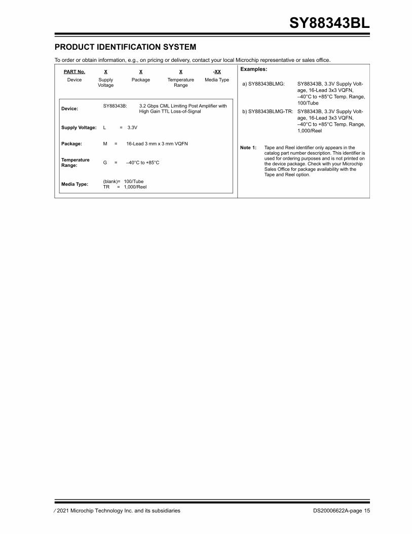
SY88343BLPRODUCT IDENTIFICATION SYSTEMTo order or obtain information, e.g., on pricing or delivery, contact your local Microchip representative or sales office.
Examples:
a) SY88343BLMG: SY88343B, 3.3V Supply Volt-age, 16-Lead 3x3 VQFN, –40°C to +85°C Temp. Range, 100/Tube
b) SY88343BLMG-TR: SY88343B, 3.3V Supply Volt-age, 16-Lead 3x3 VQFN, –40°C to +85°C Temp. Range, 1,000/Reel
Device: SY88343B: 3.2 Gbps CML Limiting Post Amplifier with High Gain TTL Loss-of-Signal
Supply Voltage: L = 3.3V
Package: M = 16-Lead 3 mm x 3 mm VQFN
Temperature Range: G = –40°C to +85°C
Media Type: (blank)= 100/TubeTR = 1,000/Reel
Note 1: Tape and Reel identifier only appears in the catalog part number description. This identifier is used for ordering purposes and is not printed on the device package. Check with your Microchip Sales Office for package availability with the Tape and Reel option.
PART No. X X X -XXDevice Supply
VoltagePackage Temperature
RangeMedia Type
SY88343BL
DS20006622A-page 16 2021 Microchip Technology Inc. and its subsidiaries
NOTES:
2021 Microchip Technology Inc. and its subsidiaries DS20006622A-page 17
This publication and the information herein may be used onlywith Microchip products, including to design, test, and integrateMicrochip products with your application. Use of this informa-tion in any other manner violates these terms. Informationregarding device applications is provided only for your conve-nience and may be superseded by updates. It is your responsi-bility to ensure that your application meets with yourspecifications. Contact your local Microchip sales office foradditional support or, obtain additional support at https://www.microchip.com/en-us/support/design-help/client-support-services.
THIS INFORMATION IS PROVIDED BY MICROCHIP "AS IS".MICROCHIP MAKES NO REPRESENTATIONS OR WAR-RANTIES OF ANY KIND WHETHER EXPRESS OR IMPLIED,WRITTEN OR ORAL, STATUTORY OR OTHERWISE,RELATED TO THE INFORMATION INCLUDING BUT NOTLIMITED TO ANY IMPLIED WARRANTIES OF NON-INFRINGEMENT, MERCHANTABILITY, AND FITNESS FOR APARTICULAR PURPOSE, OR WARRANTIES RELATED TOITS CONDITION, QUALITY, OR PERFORMANCE.
IN NO EVENT WILL MICROCHIP BE LIABLE FOR ANY INDI-RECT, SPECIAL, PUNITIVE, INCIDENTAL, OR CONSE-QUENTIAL LOSS, DAMAGE, COST, OR EXPENSE OF ANYKIND WHATSOEVER RELATED TO THE INFORMATION ORITS USE, HOWEVER CAUSED, EVEN IF MICROCHIP HASBEEN ADVISED OF THE POSSIBILITY OR THE DAMAGESARE FORESEEABLE. TO THE FULLEST EXTENTALLOWED BY LAW, MICROCHIP'S TOTAL LIABILITY ONALL CLAIMS IN ANY WAY RELATED TO THE INFORMATIONOR ITS USE WILL NOT EXCEED THE AMOUNT OF FEES, IFANY, THAT YOU HAVE PAID DIRECTLY TO MICROCHIPFOR THE INFORMATION.
Use of Microchip devices in life support and/or safety applica-tions is entirely at the buyer's risk, and the buyer agrees todefend, indemnify and hold harmless Microchip from any andall damages, claims, suits, or expenses resulting from suchuse. No licenses are conveyed, implicitly or otherwise, underany Microchip intellectual property rights unless otherwisestated.
TrademarksThe Microchip name and logo, the Microchip logo, Adaptec, AnyRate, AVR, AVR logo, AVR Freaks, BesTime, BitCloud, CryptoMemory, CryptoRF, dsPIC, flexPWR, HELDO, IGLOO, JukeBlox, KeeLoq, Kleer, LANCheck, LinkMD, maXStylus, maXTouch, MediaLB, megaAVR, Microsemi, Microsemi logo, MOST, MOST logo, MPLAB, OptoLyzer, PIC, picoPower, PICSTART, PIC32 logo, PolarFire, Prochip Designer, QTouch, SAM-BA, SenGenuity, SpyNIC, SST, SST Logo, SuperFlash, Symmetricom, SyncServer, Tachyon, TimeSource, tinyAVR, UNI/O, Vectron, and XMEGA are registered trademarks of Microchip Technology Incorporated in the U.S.A. and other countries.
AgileSwitch, APT, ClockWorks, The Embedded Control Solutions Company, EtherSynch, Flashtec, Hyper Speed Control, HyperLight Load, IntelliMOS, Libero, motorBench, mTouch, Powermite 3, Precision Edge, ProASIC, ProASIC Plus, ProASIC Plus logo, Quiet- Wire, SmartFusion, SyncWorld, Temux, TimeCesium, TimeHub, TimePictra, TimeProvider, TrueTime, WinPath, and ZL are registered trademarks of Microchip Technology Incorporated in the U.S.A.
Adjacent Key Suppression, AKS, Analog-for-the-Digital Age, Any Capacitor, AnyIn, AnyOut, Augmented Switching, BlueSky, BodyCom, CodeGuard, CryptoAuthentication, CryptoAutomotive, CryptoCompanion, CryptoController, dsPICDEM, dsPICDEM.net, Dynamic Average Matching, DAM, ECAN, Espresso T1S, EtherGREEN, GridTime, IdealBridge, In-Circuit Serial Programming, ICSP, INICnet, Intelligent Paralleling, Inter-Chip Connectivity, JitterBlocker, Knob-on-Display, maxCrypto, maxView, memBrain, Mindi, MiWi, MPASM, MPF, MPLAB Certified logo, MPLIB, MPLINK, MultiTRAK, NetDetach, NVM Express, NVMe, Omniscient Code Generation, PICDEM, PICDEM.net, PICkit, PICtail, PowerSmart, PureSilicon, QMatrix, REAL ICE, Ripple Blocker, RTAX, RTG4, SAM-ICE, Serial Quad I/O, simpleMAP, SimpliPHY, SmartBuffer, SmartHLS, SMART-I.S., storClad, SQI, SuperSwitcher, SuperSwitcher II, Switchtec, SynchroPHY, Total Endurance, TSHARC, USBCheck, VariSense, VectorBlox, VeriPHY, ViewSpan, WiperLock, XpressConnect, and ZENA are trademarks of Microchip Technology Incorporated in the U.S.A. and other countries.
SQTP is a service mark of Microchip Technology Incorporated in the U.S.A.
The Adaptec logo, Frequency on Demand, Silicon Storage Technology, Symmcom, and Trusted Time are registered trademarks of Microchip Technology Inc. in other countries.
GestIC is a registered trademark of Microchip Technology Germany II GmbH & Co. KG, a subsidiary of Microchip Technology Inc., in other countries.
All other trademarks mentioned herein are property of their respective companies.
© 2021, Microchip Technology Incorporated and its subsidiaries.
All Rights Reserved.
ISBN: 978-1-5224-9302-0
Note the following details of the code protection feature on Microchip products:• Microchip products meet the specifications contained in their particular Microchip Data Sheet.
• Microchip believes that its family of products is secure when used in the intended manner, within operating specifications, and under normal conditions.
• Microchip values and aggressively protects its intellectual property rights. Attempts to breach the code protection features of Microchip product is strictly prohibited and may violate the Digital Millennium Copyright Act.
• Neither Microchip nor any other semiconductor manufacturer can guarantee the security of its code. Code protection does not mean that we are guaranteeing the product is “unbreakable”. Code protection is constantly evolving. Microchip is committed to continuously improving the code protection features of our products.
For information regarding Microchip’s Quality Management Systems, please visit www.microchip.com/quality.
DS20006622A-page 18 2021 Microchip Technology Inc. and its subsidiaries
AMERICASCorporate Office2355 West Chandler Blvd.Chandler, AZ 85224-6199Tel: 480-792-7200 Fax: 480-792-7277Technical Support: http://www.microchip.com/supportWeb Address: www.microchip.comAtlantaDuluth, GA Tel: 678-957-9614 Fax: 678-957-1455Austin, TXTel: 512-257-3370 BostonWestborough, MA Tel: 774-760-0087 Fax: 774-760-0088ChicagoItasca, IL Tel: 630-285-0071 Fax: 630-285-0075DallasAddison, TX Tel: 972-818-7423 Fax: 972-818-2924DetroitNovi, MI Tel: 248-848-4000Houston, TX Tel: 281-894-5983IndianapolisNoblesville, IN Tel: 317-773-8323Fax: 317-773-5453Tel: 317-536-2380Los AngelesMission Viejo, CA Tel: 949-462-9523Fax: 949-462-9608Tel: 951-273-7800 Raleigh, NC Tel: 919-844-7510New York, NY Tel: 631-435-6000San Jose, CA Tel: 408-735-9110Tel: 408-436-4270Canada - TorontoTel: 905-695-1980 Fax: 905-695-2078
ASIA/PACIFICAustralia - SydneyTel: 61-2-9868-6733China - BeijingTel: 86-10-8569-7000 China - ChengduTel: 86-28-8665-5511China - ChongqingTel: 86-23-8980-9588China - DongguanTel: 86-769-8702-9880 China - GuangzhouTel: 86-20-8755-8029 China - HangzhouTel: 86-571-8792-8115 China - Hong Kong SARTel: 852-2943-5100 China - NanjingTel: 86-25-8473-2460China - QingdaoTel: 86-532-8502-7355China - ShanghaiTel: 86-21-3326-8000 China - ShenyangTel: 86-24-2334-2829China - ShenzhenTel: 86-755-8864-2200 China - SuzhouTel: 86-186-6233-1526 China - WuhanTel: 86-27-5980-5300China - XianTel: 86-29-8833-7252China - XiamenTel: 86-592-2388138 China - ZhuhaiTel: 86-756-3210040
ASIA/PACIFICIndia - BangaloreTel: 91-80-3090-4444 India - New DelhiTel: 91-11-4160-8631India - PuneTel: 91-20-4121-0141Japan - OsakaTel: 81-6-6152-7160 Japan - TokyoTel: 81-3-6880- 3770 Korea - DaeguTel: 82-53-744-4301Korea - SeoulTel: 82-2-554-7200Malaysia - Kuala LumpurTel: 60-3-7651-7906Malaysia - PenangTel: 60-4-227-8870Philippines - ManilaTel: 63-2-634-9065SingaporeTel: 65-6334-8870Taiwan - Hsin ChuTel: 886-3-577-8366Taiwan - KaohsiungTel: 886-7-213-7830Taiwan - TaipeiTel: 886-2-2508-8600 Thailand - BangkokTel: 66-2-694-1351Vietnam - Ho Chi MinhTel: 84-28-5448-2100
EUROPEAustria - WelsTel: 43-7242-2244-39Fax: 43-7242-2244-393Denmark - CopenhagenTel: 45-4485-5910 Fax: 45-4485-2829Finland - EspooTel: 358-9-4520-820France - ParisTel: 33-1-69-53-63-20 Fax: 33-1-69-30-90-79 Germany - GarchingTel: 49-8931-9700Germany - HaanTel: 49-2129-3766400Germany - HeilbronnTel: 49-7131-72400Germany - KarlsruheTel: 49-721-625370Germany - MunichTel: 49-89-627-144-0 Fax: 49-89-627-144-44Germany - RosenheimTel: 49-8031-354-560Israel - Ra’anana Tel: 972-9-744-7705Italy - Milan Tel: 39-0331-742611 Fax: 39-0331-466781Italy - PadovaTel: 39-049-7625286 Netherlands - DrunenTel: 31-416-690399 Fax: 31-416-690340Norway - TrondheimTel: 47-7288-4388Poland - WarsawTel: 48-22-3325737 Romania - BucharestTel: 40-21-407-87-50Spain - MadridTel: 34-91-708-08-90Fax: 34-91-708-08-91Sweden - GothenbergTel: 46-31-704-60-40Sweden - StockholmTel: 46-8-5090-4654UK - WokinghamTel: 44-118-921-5800Fax: 44-118-921-5820
Worldwide Sales and Service
09/14/21