Embed Size (px)
Citation preview
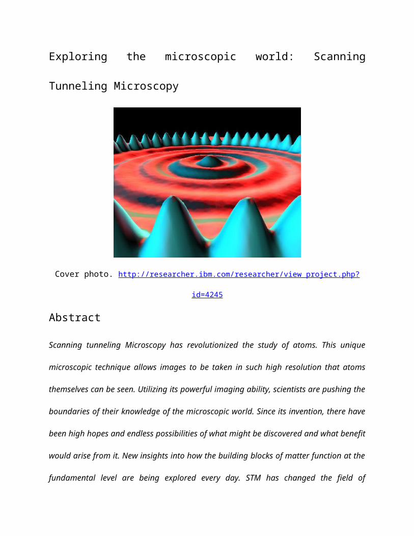
Exploring the microscopic world: Scanning Tunneling Microscopy
Cover photo. http://researcher.ibm.com/researcher/view_project.php?id=4245
Abstract
Scanning tunneling Microscopy has revolutionized the study of atoms. This unique microscopic
technique allows images to be taken in such high resolution that atoms themselves can be seen.
Utilizing its powerful imaging ability, scientists are pushing the boundaries of their knowledge of
the microscopic world. Since its invention, there have been high hopes and endless possibilities
of what might be discovered and what benefit would arise from it. New insights into how the
building blocks of matter function at the fundamental level are being explored every day. STM
has changed the field of nanotechnology forever, and it is continuing to teach scientists more
and more in various fields including engineering, physics, and chemistry.
Introduction
The world of the extremely small is very much unknown. Similar to the stars in the sky, a
scientist can’t reach out and touch anything, or physically change what he is looking at. Things
cannot be affected, only observed. Just as a powerful telescope is vital to an astronomer, a
powerful microscope is essential to exploring the very small. Scanning tunneling microscopy
(STM) has opened doors to the microscopic world. It has provided new insights to what actually
goes on at the nanoscale level. STM is a revolutionary technique that allows for images of just a
few nanometers in length to be taken with incredible resolution. Taking advantage of quantum
tunneling, ultra high vacuum conditions, and extremely low temperatures, the building blocks
of the universe, the atoms themselves are being understood and even manipulated. STM has
created a whole new style of research, with applications in engineering, physics, chemistry, and
nanotechnology. STM is literally teaching us more about this microscopic world that we know
so little about.
History
In 1981, two IBM researchers, Gerd Binnig and Heinrich Rohrer, revolutionized the science of
the very, very small with their invention of the scanning tunneling microscope [1]. Never before
could scientists peer into this microscopic world with such precision. With the ability to take
images all the way down to the size of atoms themselves, STM has opened up entirely new
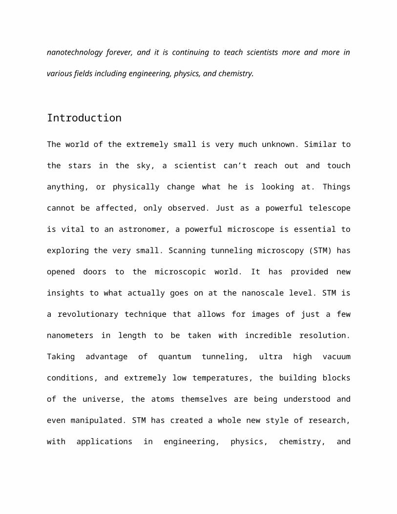
fields for the study of matter. Figure 1 shows an example of an image taken of graphite. STM is
widely regarded as the instrument that opened the door to nanotechnology and a wide range
of explorations in many diverse fields [1]. This instrument, just five years after its invention,
would win Binnig and Rohrer the Nobel prize in physics in 1986 [2]. In addition to changing the
field of microscopic study forever, it also led to the invention of other sorts of high resolution
microscopic instruments that together continue to teach us more about the world of the very
small.
Figure 1. This is an STM image of graphite. The outlines in the picture are the hexagonal structures of the
carbon atoms of graphite bonded together. Brighter spots correspond to more electrons reaching the
tip, distinguishing the layers of the graphite.
How it works
STM synonymously stands for both the scanning tunneling microscope, as well as the scanning
tunneling microscopic technique. This technique allows for images of just a few nanometers to
be taken with surprisingly clear resolution. It does so by taking advantage of quantum
tunneling, a process to be explained soon. Basically, an atomically sharp tip, that is a tip with
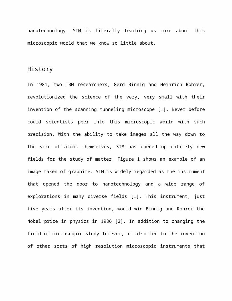
one atom at the very end, is brought very close to a conductive surface. Figure 2 shows a
picture of an STM tip. The tip slowly scans across the surface at a distance of only an atom's
diameter [7]. At this small distance electrons can tunnel into the tip, from the surface,
producing a measurable current. Figure 3 illustrates this principle.
Figure 2. This is a picture of an STM tip taken by a different type of microscope.
http://www.ieap.uni-kiel.de/surface/ag-kipp/stm/stm.htm
Figure 3. An atomically sharp tip is brought within nanometers of a surface. Once close enough, the
electrons will tunnel the gap between surface and tip.
Tunneling is a quantum mechanical phenomenon that only occurs with particles small enough
to exhibit quantum behavior, in this particular case electrons. Real, everyday objects (macro
scale) are governed by classical/Newtonian mechanics, not quantum mechanics. In other words
tunneling is not a phenomenon one can observe with the eyes. Tunneling is the process of a
particle overcoming a barrier that classically it cannot overcome. To put it in simple terms let’s
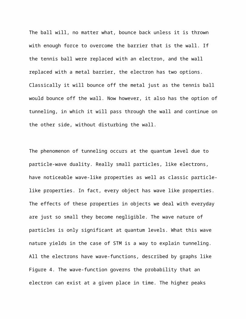
look at an example. Imagine a person throwing a tennis ball at a wall. Classically what will
happen? The ball will, no matter what, bounce back unless it is thrown with enough force to
overcome the barrier that is the wall. If the tennis ball were replaced with an electron, and the
wall replaced with a metal barrier, the electron has two options. Classically it will bounce off the
metal just as the tennis ball would bounce off the wall. Now however, it also has the option of
tunneling, in which it will pass through the wall and continue on the other side, without
disturbing the wall.
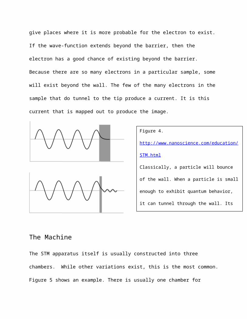
The phenomenon of tunneling occurs at the quantum level due to particle-wave duality. Really
small particles, like electrons, have noticeable wave-like properties as well as classic particle-
like properties. In fact, every object has wave like properties. The effects of these properties in
objects we deal with everyday are just so small they become negligible. The wave nature of
particles is only significant at quantum levels. What this wave nature yields in the case of STM is
a way to explain tunneling. All the electrons have wave-functions, described by graphs like
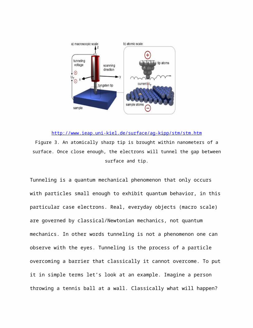
Figure 4. The wave-function governs the probability that an electron can exist at a given place in
time. The higher peaks give places where it is more probable for the electron to exist. If the
wave-function extends beyond the barrier, then the electron has a good chance of existing
beyond the barrier. Because there are so many electrons in a particular sample, some will exist
beyond the wall. The few of the many electrons in the sample that do tunnel to the tip produce
a current. It is this current that is mapped out to produce the image.
The Machine
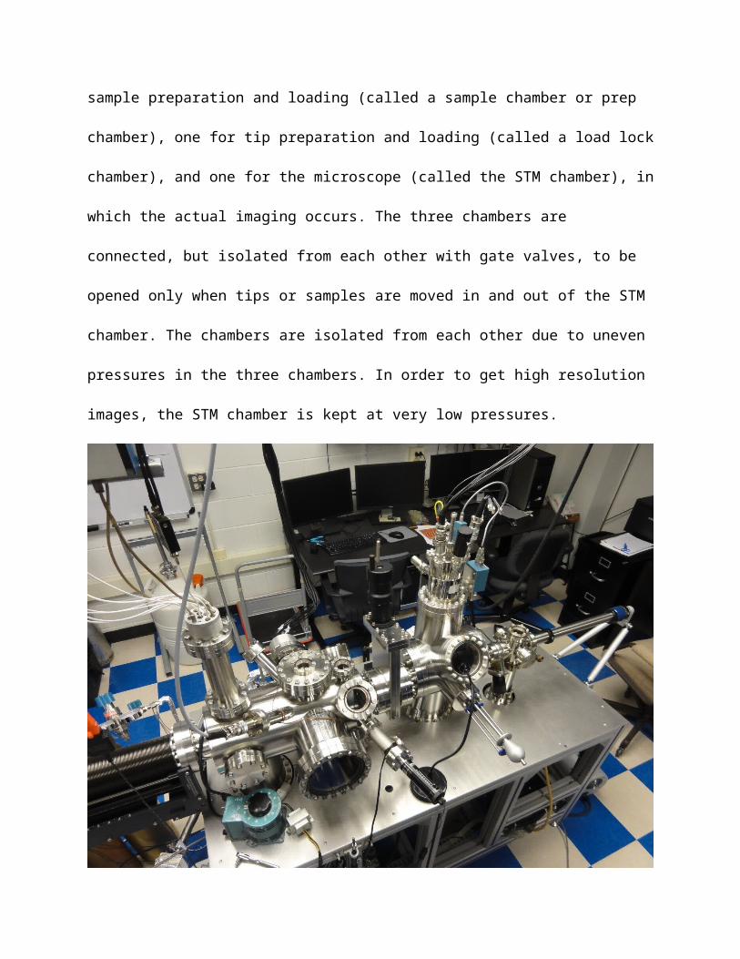
The STM apparatus itself is usually constructed into three chambers. While other variations
exist, this is the most common. Figure 5 shows an example. There is usually one chamber for
sample preparation and loading (called a sample chamber or prep chamber), one for tip
preparation and loading (called a load lock chamber), and one for the microscope (called the
STM chamber), in which the actual imaging occurs. The three chambers are connected, but
isolated from each other with gate valves, to be opened only when tips or samples are moved
Figure 4.
http://www.nanoscience.com/education/STM.html
Classically, a particle will bounce of the wall. When a
particle is small enough to exhibit quantum behavior, it
can tunnel through the wall. Its wave function can
extend beyond the barrier if it is small enough. If the
wave function does, the electron can essentially exist
beyond the barrier.
in and out of the STM chamber. The chambers are isolated from each other due to uneven
pressures in the three chambers. In order to get high resolution images, the STM chamber is
kept at very low pressures.
Figure 5. This is a picture of an STM instrument. The leftmost chamber is the preparation chamber,
where samples to be imaged are prepared. The middle chamber is the STM chamber where the actual
imaging occurs. The rightmost chamber (much smaller than the other two) is the load lock, where STM
tips are loaded into the STM chamber.
The microscope is very sensitive. Remember, it is taking nanoscale images. Even the slightest
vibrations in the surroundings can disturb images. Because of this sensitivity, the STM
apparatus is pumped down to ultra-high vacuum (UHV) conditions. It is not uncommon for the
STM chamber to be at pressures of 10-11 Torr, an incredibly low pressure. To put this into
perspective, atmospheric conditions, what you and I are likely feeling right now, is about 760
Torr. The STM Chamber is engineered to withstand pressures of 13 orders of magnitude less
than atmosphere! These low pressures are referred to as ultra-high vacuum conditions. Keep in
mind that even at ultra-high vacuum, these low temperatures do not produce a perfect
vacuum. In a theoretical sense, vacuum is empty space, the existence of nothing in a given area.
There are still molecules in the air of the chamber at these low pressures, but a significantly
lower amount than at atmospheric conditions. Ultra-high vacuum is obtained using a
combination of various pumps. The ion pump is generally the pump utilized by STM to achieve
its lowest pressures. Ion pumps remove gases from their environment by charging the
molecules and then attracting them with a high magnetic field [3]. This removes the air from
chamber, by sucking it into the pump. The absence of the molecules in the space of the
chamber is what generates the low pressure.
In addition to low pressures, the chamber is also built to withstand low temperatures. At the
fundamental level all atoms vibrate. The STM is attempting to image these vibrating atoms. It is
easy to see that reducing the vibration will be a great help in getting clearer images. To reduce
the drift of the molecules the STM can be cooled all the way to 4K (-269 °C or -452 °F) using
liquid helium [4]. That’s 4 degrees above absolute zero! These low temperatures reduce
significantly the thermal drift of the molecules because the lower the temperature, the slower
the molecules will vibrate. With as many molecules out of the way as possible and the
instrument as cold as can be, electrons have fewer obstacles to overcome in tunneling the
space between surface and tip. With a good flow of electrons into the STM probe, scientists can
get images of high resolution.
Applications
Binnig and Rohrer’s breakthrough invention was the starting point for research in
nanotechnology [1]. It has found applications in engineering, physics, chemistry, and materials
science. It is a tool scientists use to learn about the nature of the nanoscale world. In learning
more and more about the building blocks of matter, scientists have high hopes in developing
new, smarter technologies, whose foundations stand in the newfound knowledge of the atomic
world. More than 20 years ago, an IBM researcher named Dr. Eigler, using STM succeeded in
moving atoms themselves. He rearranged them to make the smallest logo ever designed as
seen in Figure 6. Understanding the properties, movement, and interaction of various materials
at the nanoscale is essential for one day building smaller, faster, and more energy efficient
processes and memory devices [5]. With the ability to understand and manipulate atoms,
scientists hope to develop personalized health care and targeted treatments and therapies.
Many industrial processes make use of chemical reactions. These reactions however are very
inefficient at the fundamental level. In some cases, one out of a trillion molecules will react the
way they are wanted to. STM is teaching scientists why reactions like this are inefficient. If they
can discover ways to make the yield increase to even one out of a million, a company’s
production will have increased by a factor of one million. It is discoveries like these that make
STM such an important tool.
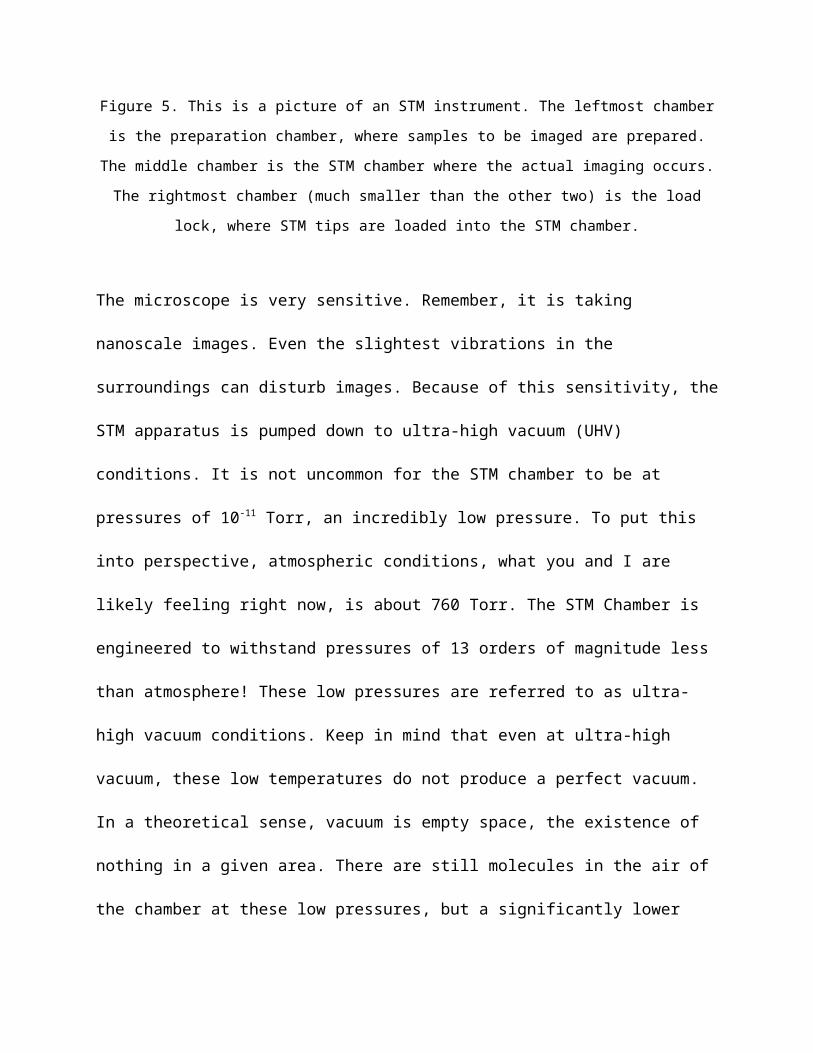
Figure 6 (includes all 3 images). These are images taken with STM after the repositioning of atoms. The
IBM logo was the first time atoms have ever been moved in this fashion before.
http://www.nobelprize.org/educational/physics/microscopes/scanning/gallery/10.html
http://researcher.ibm.com/researcher/view_project_subpage.php?id=4253
ConclusionScanning tunneling microscopy has created a new way in which scientists can observe the
world. The building blocks of our universe can be observed and even manipulated with STM.
Making use of this technique, scientists and engineers can research and design new materials
and products from a nanoscale foundation. For a long time, the microscopic world was just like
the cosmic world, the atoms like the stars in the sky. You couldn’t touch them, or change them,
only observe them. STM has invalidated this analogy. The stars of the microscopic world are
being studied and even moved like the stars in the sky may never be. STM and the instruments
and techniques it has paved the way for will continue to make discoveries in this microscopic
world, and these discoveries will likely continue to amaze us.
[1] IBM, Scanning Tunneling Microscope [Online].
Available:http://www-03.ibm.com/ibm/history/ibm100/us/en/icons/microscope/
[2] Nanoscience Instruments, Scanning Tunneling Microscopy [Online]. Available:
http://www.nanoscience.com/education/STM.html
[3] Gamma Vacuum, Ion Pump Technology [Online]. Available:
http://www.gammavacuum.com/operation.asp
[4] Encyclopædia Britannica, scanning tunneling microscope (STM) [Online]. Available:
http://www.britannica.com/EBchecked/topic/526582/scanning-tunneling-microscope-STM/
285634/Applications
[5] YouTube, IBM Celebrates 20th Anniversary of Moving Atoms [Online]. Available:
http://www.youtube.com/watch?v=0wF4f2YadoA
[6] History of the Microscope, Who invented the microscope? A complete Microscope History
[Online]. Available: http://www.history-of-the-microscope.org/history-of-the-microscope-who-
invented-the-microscope.php
[7] Nobel Prize, The Scanning Tunneling Microscope [Online]. Available:
http://www.nobelprize.org/educational/physics/microscopes/scanning/