Embed Size (px)
Citation preview

8/8/2019 348039_1
http://slidepdf.com/reader/full/3480391 1/11
LM1036
Dual DC Operated Tone/Volume/Balance Circuit
General DescriptionThe LM1036 is a DC controlled tone (bass/treble), volumeand balance circuit for stereo applications in car radio, TVand audio systems. An additional control input allows loud-ness compensation to be simply effected.
Four control inputs provide control of the bass, treble, bal-ance and volume functions through application of DC volt-ages from a remote control system or, alternatively, from fourpotentiometers which may be biased from a zener regulatedsupply provided on the circuit.
Each tone response is defined by a single capacitor chosento give the desired characteristic.
Featuresn Wide supply voltage range, 9V to 16V
n Large volume control range, 75 dB typical
n Tone control, ±15 dB typical
n Channel separation, 75 dB typical
n Low distortion, 0.06% typical for an input level of 0.3Vrms
n High signal to noise, 80 dB typical for an input level of0.3 Vrms
n Few external components required
Block and Connection Diagram
Dual-In-Line Package
DS005142-1
Order Number LM1036NSee NS Package Number N20A
January 1995
L M1 0 3 6 D u al D C
O p e r a t e d T on e /
V ol u m e / B al an c e C i r c ui t
© 1999 National Semiconductor Corporation DS005142 www.national.com
8/8/2019 348039_1
http://slidepdf.com/reader/full/3480391 2/11
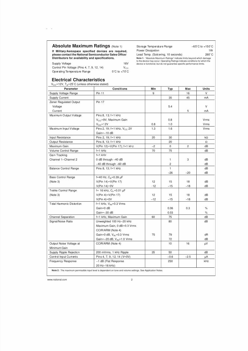
Absolute Maximum Ratings (Note 1)
If Military/Aerospace specified devices are required,please contact the National Semiconductor Sales Office/
Distributors for availability and specifications.
Supply Voltage 16V
Control Pin Voltage (Pins 4, 7, 9, 12, 14) VCC
Operat ing Temperature Range 0˚C to +70 C
Storage Temperat ure Range −65 C to +150 C
Power Dissipation 1W
Lead Temp. (Soldering, 10 seconds) 260˚ CNote 1: “Absolute Maximum Ratings” indicate limits beyond which damage
to the device may occur. Operating Ratings indicate conditions for which thedevice is functional, but do not guarantee specific performance limits.
Electrical CharacteristicsVCC
=12V, TA=25˚C (unless otherwise stated)
Parameter Conditions Min Typ Max Units
Supply Voltage Range Pin 11 9 16 V
Supply Current 35 45 mA
Zener Regulated Output Pin 17
Voltage 5.4 V
Current 5 mA
Maximum Output Voltage Pins 8, 13; f=1 kHz
VCC=9V, Maximum Gain 0.8 Vrms
VCC=12V 0.8 1.0 Vrms
Maximum Input V ol tage P ins 2, 19; f=1 kHz, VCC 2V 1.3 1.6 Vrms
Gain=−10 dB
Input Resistance Pins 2, 19; f=1 kHz 20 30 kΩ
Output Resistance Pins 8, 13; f=1 kHz 20 Ω
Maximum Gain V(Pin 12)=V(Pin 17); f=1 kHz −2 0 2 dB
Volume Control Range f=1 kHz 70 75 dB
Gain Tracking f=1 kHz
Channel 1–Channel 2 0 dB through −40 dB 1 3 dB
−40 dB through −60 dB 2 dB
Balance Control Range Pins 8, 13; f=1 kHz 1 dB
−26 −20 dB
Bass Control Range f=40 Hz, Cb=0.39 µF
(Note 3) V(Pin 14)=V(Pin 17) 12 15 18 dB
V(Pin 14)=0V −12 −15 −18 dB
Treble Control Range f= 16 kHz, Ct,=0.01 µF
(Note 3) V(Pin 4)=V(Pin 17) 12 15 18 dB
V(Pin 4)=0V −12 −15 −18 dB
Total Harmonic D istorti on f=1 kHz, VIN=0.3 Vrms
Gain=0 dB 0.06 0.3 %
Gain=−30 dB 0.03 %
Channel Separation f=1 kHz, Maximum Gain 60 75 dB
Signal/Noise Ratio Unweighted 100 Hz–20 kHz 80 dB
Maximum Gain, 0 dB=0.3 Vrms
CCIR/ARM (Note 4)
Gain=0 dB, VIN=0.3 Vrms 75 79 dB
Gain=−20 dB, VIN=1.0 Vrms 72 dB
Output Noise Voltage at CCIR/ARM (Note 4) 10 16 µV
Minimum Gain
Supply Ripple Rejection 200 mVrms, 1 kHz Ripple 35 50 dB
Control Input Current s P ins 4, 7, 9, 12, 14 (V=0V) −0.6 −2.5 µA
Frequency Response −1 dB (Flat Response 250 kHz
20 Hz–16 kHz)
Note 2: The maximum permissible input level is dependent on tone and volume settings. See Application Notes.
www.national.com 2
8/8/2019 348039_1
http://slidepdf.com/reader/full/3480391 3/11
Electrical Characteristics (Continued)
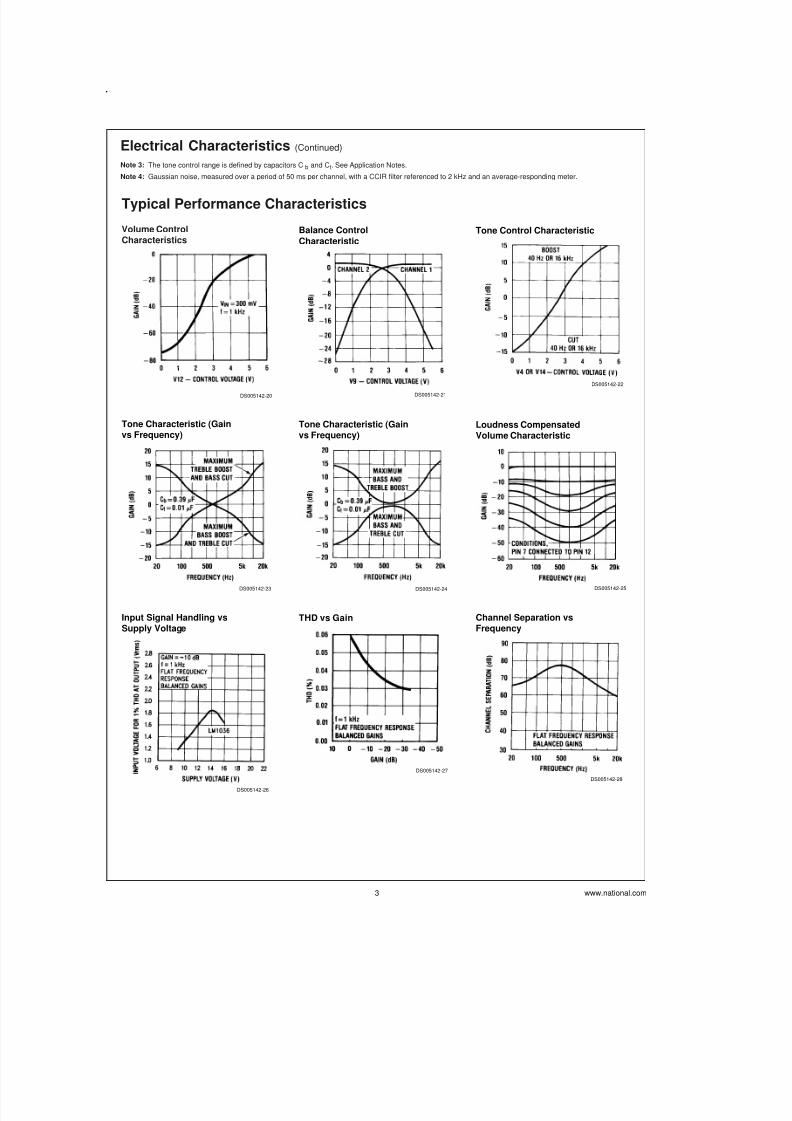
Note 3: The tone control range is defined by capacitors Cb and Ct. See Application Notes.
Note 4: Gaussian noise, measured over a period of 50 ms per channel, with a CCIR filter referenced to 2 kHz and an average-responding meter.
Typical Performance Characteristics
Volume ControlCharacteristics
DS005142-20
Balance Control
Characteristic
DS005142-21
Tone Control Characteristic
DS005142-22
Tone Characteristic (Gainvs Frequency)
DS005142-23
Tone Characteristic (Gainvs Frequency)
DS005142-24
Loudness CompensatedVolume Characteristic
DS005142-25
Input Signal Handling vsSupply Voltage
DS005142-26
THD vs Gain
DS005142-27
Channel Separation vsFrequency
DS005142-28
www.national.com3

8/8/2019 348039_1
http://slidepdf.com/reader/full/3480391 4/11
Typical Performance Characteristics (Continued)
Application NotesTONE RESPONSE
The maximum boost and cut can be optimized for individualapplications by selection of the appropriate values of Ct
(treble) and Cb (bass).
The tone responses are defined by the relationships:
Where ab=at=0 for maximum bass and treble boost respec-tively and ab=at=1 for maximum cut.
For the values of Cb and Ct of 0.39 µF and 0.01 µF as shownin the Application Circuit, 15 dB of boost or cut is obtained at40 Hz and 16 kHz.
ZENER VOLTAGE
A zener voltage (pin 17=5.4V) is provided which may beused to bias the control potentiometers. Setting a DC level ofone half of the zener voltage on the control inputs, pins 4, 9,and 14, results in the balanced gain and flat response condi-tion. Typical spread on the zener voltage is ±100 mV andthis must be taken into account if control signals are usedwhich are not referenced to the zener voltage. If this is thecase, then they will need to be derived with similar accuracy.
LOUDNESS COMPENSATION
A simple loudness compensation may be effected by apply-ing a DC control voltage to pin 7. This operates on the tonecontrol stages to produce an additional boost limited by the
maximum boost defined by Cb and Ct. There is no loudnesscompensation when pin 7 is connected to pin 17. Pin 7 canbe connected to pin 12 to give the loudness compensatedvolume characteristic as illustrated without the addition offurther external components. (Tone settings are for flat re-sponse, Cb and Ct as given in Application Circuit.) Modifica-tion to the loudness characteristic is possible by changingthe capacitors Cb and Ct for a different basic response or, bya resistor network between pins 7 and 12 for a differentthreshold and slope.
SIGNAL HANDLING
The volume control function of the LM1036 is carried out intwo stages, controlled by the DC voltage on pin 12, to im-prove signal handling capability and provide a reduction ofoutput noise level at reduced gain. The first stage is beforethe tone control processing and provides an initial 15 dB ofgain reduction, so ensuring that the tone sections are notoverdriven by large input levels when operating with a low
volume setting. Any combination of tone and volume settingsmay be used provided the output level does not exceed1 Vrms, VCC
=12V (0.8 Vrms, VCC=9V). At reduced gain
(<−6 dB)the input stage will overload if the input level ex-ceeds 1.6 Vrms, VCC
=12V (1.1 Vrms, VCC=9V). As there is
volume control on the input stages, the inputs may be oper-ated with a lower overload margin than would otherwise beacceptable, allowing a possible improvement in signal tonoise ratio.
Loudness ControlCharacteristic
DS005142-29
Output Noise Voltage
vs Gain
DS005142-30
THD vs Input Voltage
DS005142-31
www.national.com 4

8/8/2019 348039_1
http://slidepdf.com/reader/full/3480391 5/11
Application Circuit
Applications InformationOBTAINING MODIFIED RESPONSE CURVES
The LM1036 is a dual DC controlled bass, treble, balanceand volume integrated circuit ideal for stereo audio systems.
In the various applications where the LM1036 can be used,there may be requirements for responses different to thoseof the standard application circuit given in the data sheet.This application section details some of the simple variationspossible on the standard responses, to assist the choice of
optimum characteristics for particular applications.
TONE CONTROLS
Summarizing the relationship given in the data sheet, basi-cally for an increase in the treble control range Ct must be in-creased, and for increased bass range Cb must be reduced.
Figure 1 shows the typical tone response obtained in thestandard application circuit. (Ct
=0.01 µF, Cb=0.39 µF). Re-
sponse curves are given for various amounts of boost andcut.
Figure 2 and Figure 3 show the effect of changing the re-sponse defining capacitors Ct and Cb to 2Ct, Cb /2 and 4Ct,Cb /4 respectively, giving increased tone control ranges. Thevalues of the bypass capacitors may become significant andaffect the lower frequencies in the bass response curves.
DS005142-3
DS005142-4
FIGURE 1. Tone Characteristic (Gain vs Frequency)
DS005142-5
FIGURE 2. Tone Characteristic (Gain vs Frequency)
DS005142-6
FIGURE 3. Tone Characteristic (Gain vs Frequency)
www.national.com5
8/8/2019 348039_1
http://slidepdf.com/reader/full/3480391 6/11
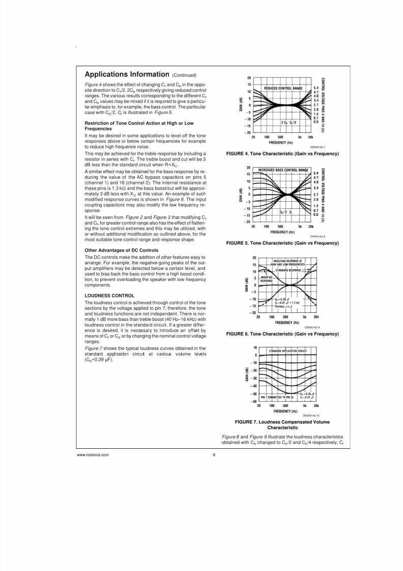
Applications Information (Continued)
Figure 4 shows the effect of changing Ct and Cb in the oppo-site direction to Ct /2, 2Cb respectively giving reduced controlranges. The various results corresponding to the different Ct
and Cb values may be mixed if it is required to give a particu-lar emphasis to, for example, the bass control. The particularcase with Cb /2, Ct is illustrated in Figure 5 .
Restriction of Tone Control Action at High or LowFrequencies
It may be desired in some applications to level off the toneresponses above or below certain frequencies for exampleto reduce high frequence noise.
This may be achieved for the treble response by including aresistor in series with Ct. The treble boost and cut will be 3dB less than the standard circuit when R=XC.
A similar effect may be obtained for the bass response by re-ducing the value of the AC bypass capacitors on pins 5(channel 1) and 16 (channel 2). The internal resistance atthese pins is 1.3 kΩ and the bass boost/cut will be approxi-mately 3 dB less with XC at this value. An example of such
modified response curves is shown in Figure 6 . The inputcoupling capacitors may also modify the low frequency re-sponse.
It will be seen from Figure 2 and Figure 3 that modifying Ct
and Cb for greater control range also has the effect of flatten-ing the tone control extremes and this may be utilized, withor without additional modification as outlined above, for themost suitable tone control range and response shape.
Other Advantages of DC Controls
The DC controls make the addition of other features easy toarrange. For example, the negative-going peaks of the out-put amplifiers may be detected below a certain level, andused to bias back the bass control from a high boost condi-tion, to prevent overloading the speaker with low frequencycomponents.
LOUDNESS CONTROL
The loudness control is achieved through control of the tonesections by the voltage applied to pin 7; therefore, the toneand loudness functions are not independent. There is nor-mally 1 dB more bass than treble boost (40 Hz–16 kHz) withloudness control in the standard circuit. If a greater differ-ence is desired, it is necessary to introduce an offset bymeans of Ct or Cb or by changing the nominal control voltageranges.
Figure 7 shows the typical loudness curves obtained in thestandard application circuit at various volume levels(Cb
=0.39 µF).
Figure 8 and Figure 9 illustrate the loudness characteristicsobtained with Cb changed to Cb /2 and Cb /4 respectively, Ct
DS005142-7
FIGURE 4. Tone Characteristic (Gain vs Frequency)
DS005142-8
FIGURE 5. Tone Characteristic (Gain vs Frequency)
DS005142-9
FIGURE 6. Tone Characteristic (Gain vs Frequency)
DS005142-10
FIGURE 7. Loudness Compensated Volume
Characteristic
www.national.com 6

8/8/2019 348039_1
http://slidepdf.com/reader/full/3480391 7/11
Applications Information (Continued)
being kept at the nominal 0.01 µF. These values naturallymodify the bass tone response as in Figure 2 and Figure 3 .
With pins 7 (loudness) and 12 (volume) directly connected,loudness control starts at typically −8 dB volume, with mostof the control action complete by −30 dB.
Figure 10 and Figure 11 show the effect of resistively offset-ting the voltage applied to pin 7 towards the control refer-ence voltage (pin 17). Because the control inputs are highimpedance, this is easily done and high value resistors maybe used for minimal additional loading. It is possible to re-duce the rate of onset of control to extend the active range to−50 dB volume control and below.
The control on pin 7 may also be divided down towardsground bringing the control action on earlier. This is illus-trated in Figure 12 , With a suitable level shifting network be-tween pins 12 and 7, the onset of loudness control and itsrate of change may be readily modified.
DS005142-11
FIGURE 8. Loudness Compensated VolumeCharacteristic
DS005142-12
FIGURE 9. Loudness Compensated Volume
Characteristic
DS005142-13
FIGURE 10. Loudness Compensated VolumeCharacteristic
DS005142-14
FIGURE 11. Loudness Compensated Volume
Characteristic
DS005142-15
FIGURE 12. Loudness Compensated Volume Characteristic
www.national.com7
8/8/2019 348039_1
http://slidepdf.com/reader/full/3480391 8/11
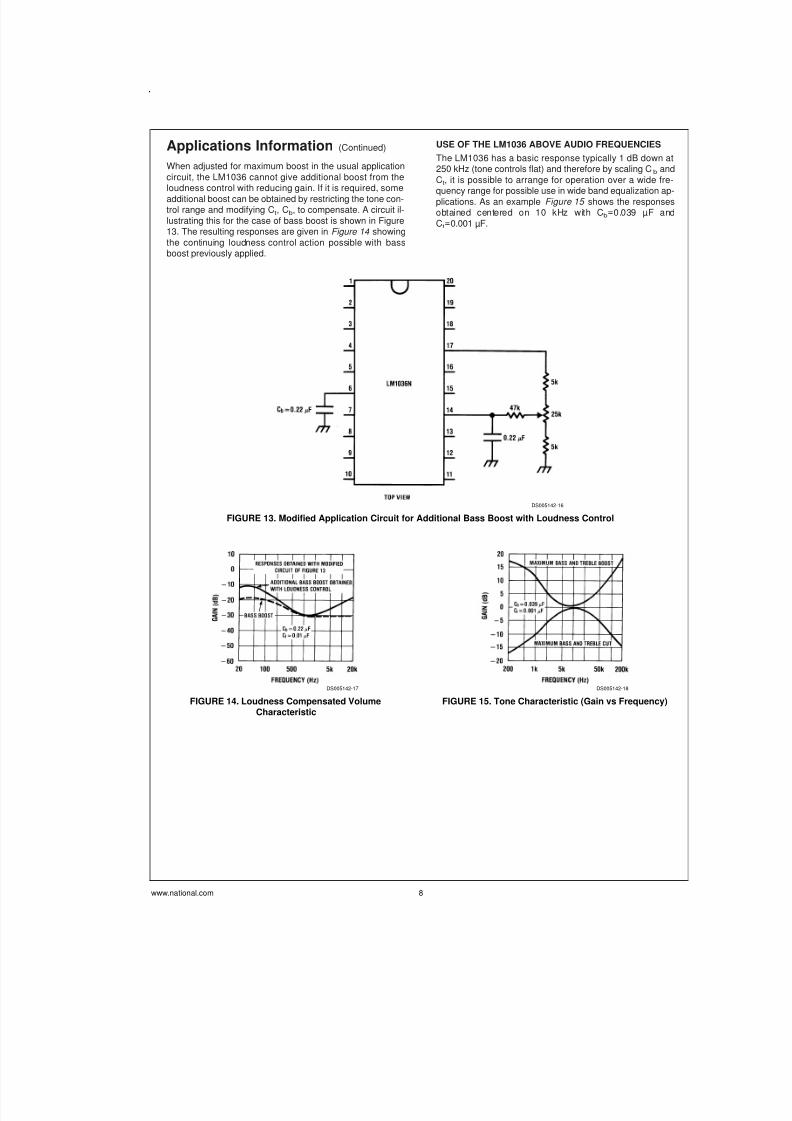
Applications Information (Continued)
When adjusted for maximum boost in the usual applicationcircuit, the LM1036 cannot give additional boost from theloudness control with reducing gain. If it is required, some
additional boost can be obtained by restricting the tone con-trol range and modifying Ct, Cb, to compensate. A circuit il-lustrating this for the case of bass boost is shown in Figure13. The resulting responses are given in Figure 14 showingthe continuing loudness control action possible with bassboost previously applied.
USE OF THE LM1036 ABOVE AUDIO FREQUENCIES
The LM1036 has a basic response typically 1 dB down at250 kHz (tone controls flat) and therefore by scaling C b andCt, it is possible to arrange for operation over a wide fre-quency range for possible use in wide band equalization ap-plications. As an example Figure 15 shows the responsesobtained centered on 10 kHz with Cb
=0.039 µF andCt
=0.001 µF.
DS005142-16
FIGURE 13. Modified Application Circuit for Additional Bass Boost with Loudness Control
DS005142-17
FIGURE 14. Loudness Compensated VolumeCharacteristic
DS005142-18
FIGURE 15. Tone Characteristic (Gain vs Frequency)
www.national.com 8

8/8/2019 348039_1
http://slidepdf.com/reader/full/3480391 9/11
Simplified Schematic Diagram (One Channel)
DS005142-19
*Connections reversed
www.national.com9

8/8/2019 348039_1
http://slidepdf.com/reader/full/3480391 10/11
Physical Dimensions inches (millimeters) unless otherwise noted
LIFE SUPPORT POLICY
NATIONAL’S PRODUCTS ARE NOT AUTHORIZED FOR USE AS CRITICAL COMPONENTS IN LIFE SUPPORTDEVICES OR SYSTEMS WITHOUT THE EXPRESS WRITTEN APPROVAL OF THE PRESIDENT AND GENERALCOUNSEL OF NATIONAL SEMICONDUCTOR CORPORATION. As used herein:
1. Life support devices or systems are devices orsystems which, (a) are intended for surgical implantinto the body, or (b) support or sustain life, andwhose failure to perform when properly used inaccordance with instructions for use provided in the
labeling, can be reasonably expected to result in asignificant injury to the user.
2. A critical component is any component of a lifesupport device or system whose failure to performcan be reasonably expected to cause the failure ofthe life support device or system, or to affect itssafety or effectiveness.
National Semiconductor
Corporation
Americas
Tel: 1-800-272-9959
Fax: 1-800-737-7018
Email: [email protected]
National Semiconductor
Europe
Fax: +49 (0) 1 80-530 85 86
Email: [email protected]
Deutsch Tel: +49 (0) 1 80-530 85 85
English Tel: +49 (0) 1 80-532 78 32
Français Tel: +49 (0) 1 80-532 93 58
Italiano Tel: +49 (0) 1 80-534 16 80
National Semiconductor
Asia Pacific Customer
Response Group
Tel: 65-2544466
Fax: 65-2504466
Email: [email protected]
National Semiconductor
Japan Ltd.
Tel: 81-3-5639-7560
Fax: 81-3-5639-7507
www.national.com
Molded Dual-In-Line Package (N)Order Number LM1036N
NS Package Number N20A
L M 1 0 3 6 D u a l D C
O p e r
a t e d T o n e / V o l u m e / B a l a n c e C i r c u i t
National does not assume any responsibility for use of any circuitry described, no circuit patent licenses are implied and National reserves the right at any time without notice to change said circuitry and specifications.

8/8/2019 348039_1
http://slidepdf.com/reader/full/3480391 11/11
This datasheet has been downloaded from:
www.DatasheetCatalog.com
Datasheets for electronic components.


