Embed Size (px)
Citation preview
354 IEEE JOURNAL OF QUANTUM ELECTRONICS, VOL. 44, NO. 4, APRIL 2008
Output Saturation and Linearity of WaveguideUnitraveling-Carrier Photodiodes
Jonathan Klamkin, Student Member, IEEE, Yu-Chia Chang, Anand Ramaswamy, Student Member, IEEE,Leif A. Johansson, Member, IEEE, John E. Bowers, Fellow, IEEE, Steven P. DenBaars, Fellow, IEEE, and
Larry A. Coldren, Fellow, IEEE
Abstract—Waveguide unitraveling-carrier photodiodes(UTC-PDs) with different absorber and collector layer dopinglevels have been fabricated and characterized. These photodiode(PD) structures are fabricated on a platform that allows forthe monolithic integration of multiquantum-well optical phasemodulators and couplers for realizing novel coherent receivers.Compared to PD A, PD B has a lower and more graded p-dopingprofile in the absorber layer and also a higher n-doping level in thecollector layer. For PD B a larger field is induced in the absorberlayer at high photocurrent levels. Also the higher n-doping in thecollector layer is adequate for providing charge compensation.For PD B, there is an enhancement in the RF response as thephotocurrent level is increased. At a frequency of 1 GHz, thesaturation current for PD A is around 65 mA and that for PD B isaround 63 mA. For PD B, the third-order output intercept pointat photocurrent levels of 30 and 40 mA is 37.2 and 34.9 dBm, re-spectively. That for PD A is 35.8 and 30.4 dBm. PD B is, therefore,favorable for linear operation at high current levels.
Index Terms—Coherent receiver, fiber-optic link, linearity, sat-uration current, third-order intermodulation distortion (IMD3),third-order output intercept point (OIP3), unitraveling-carrierphotodiode (UTC-PD).
I. INTRODUCTION
COHERENT fiber-optic links that utilize phase modulationcan demonstrate high spur-free dynamic range and high
signal-to-noise ratio. The challenge with phase modulation isbuilding a coherent receiver that can linearly demodulate thephase of the received signal. To overcome this, we have demon-strated a novel coherent receiver architecture employing feed-back for closely tracking the phase of the received signal [1],[2]. The incoming signal is mixed with a local oscillator signaland the detected photocurrent representing the phase differenceis then fed back to a reference phase modulator. For high loopgain the signal phase is tracked closely. With a monolithicallyintegrated approach, the delay of the feedback can be kept shortenough for operation in the gigahertz (GHz) frequency range.
A very important requirement of this coherent receiver is therealization of photodiodes (PDs) that demonstrate both highoutput saturation current and high linearity at GHz frequen-cies and can be monolithically integrated with optical phase
Manuscript received July 24, 2007; revised October 9, 2007. Thiswork was supported by the Defense Advanced Research Projects Agency(DARPA) PHOR-FRONT program under United States Air Force ContractFA8750-05-C-0265.
The authors are with the Materials Department and the Electrical and Com-puter Engineering Department at the University of California, Santa Barbara,CA 93106 USA (e-mail: [email protected]).
Digital Object Identifier 10.1109/JQE.2007.914768
modulators and couplers. The unitraveling-carrier photodiode(UTC-PD) is designed for high speed and high current operation[3]. We have previously demonstrated a monolithic balancedUTC-PD with a tunable multimode interference coupler on aplatform that allows for the integration of MQW phase modula-tors [4]. In a UTC-PD light is absorbed in an undepleted p-typenarrow bandgap layer, referred to as the absorber, and photo-generated electrons subsequently diffuse to a wide bandgap driftlayer, referred to as the collector. Electrons are the only activecarriers and electrons have a higher drift velocity than holes,therefore space charge saturation effects are reduced when com-pared to a p-i-n PD.
Several techniques for improving the performance ofUTC-PDs have been demonstrated. Charge compensationwas used to improve the saturation current by intentionallyn-doping the collector layer [5]. By doing so, the electric fieldis preconditioned to be higher in the presence of a large mobilespace charge density. Others have reported an enhancement inthe response of UTC-PDs that have a graded doping profilein the p-type absorber [6]. This grade results in a potentialprofile that can aid electron transport. This same effect wasalso observed for UTC-PDs with uniform but relatively lowerabsorber doping [7].
We previously reported waveguide UTC-PDs that demon-strated output saturation currents greater than 40 mA at 1 GHzand a third-order output intercept point (OIP3) of 43 dBm at20 mA and 34 dBm at 40 mA [8]. We observed a significantimprovement in the saturation characteristics for devices thathad a wider input waveguide. Here we have closely investi-gated the effects of the doping profile in several layers of theUTC-PD structure on the output response, saturation current,and third-order intermodulation distortion (IMD3). In partic-ular, two different waveguide UTC-PDs were fabricated andcharacterized. The most significant differences in these devicesare the doping profiles in the absorber and collector layers. Thedevices are referred to as PD A and PD B. In PD A, the p-dopingin the absorber layer is not only higher, but also more uniform.The n-doping in the collector layer of PD A is 7E15 cmwhereas that for PD B is 6E16 cm . For PD B an enhance-ment in the output response is observed at high current. Thisis believed to be due to the combination of the lower and moregraded absorber doping profile as well as the higher collectordoping level. The lower and more graded doping level in the ab-sorber results in a small field induced at high current levels, andthe higher collector doping level provides charge compensation.Both PDs exhibit saturation current levels that, to the best of ourknowledge, are some of the highest reported for waveguide PDs
0018-9197/$25.00 © 2008 IEEE
KLAMKIN et al.: OUTPUT SATURATION AND LINEARITY OF WAVEGUIDE UTC PDs 355
TABLE IUTC-PD LAYER STRUCTURE
at comparable frequencies. For PD B, the OIP3 increases withphotocurrent more so than for PD A. PD B exhibits higher lin-earity at high photocurrent levels.
II. DEVICE DESIGN AND FABRICATION
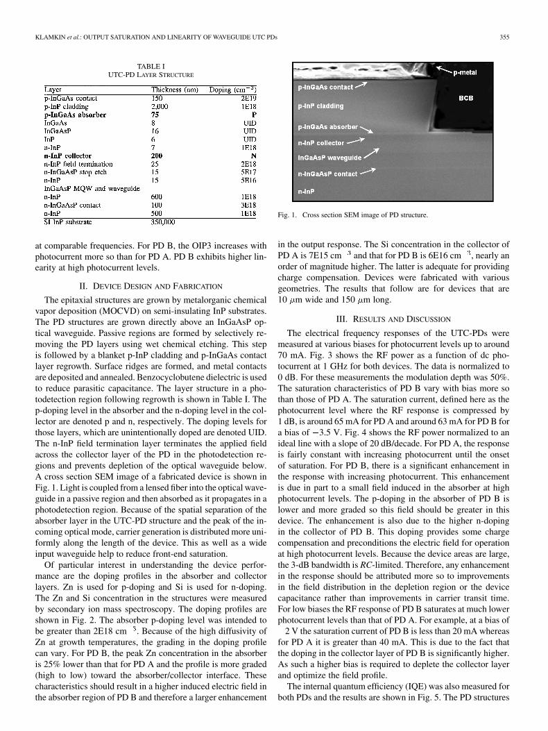
The epitaxial structures are grown by metalorganic chemicalvapor deposition (MOCVD) on semi-insulating InP substrates.The PD structures are grown directly above an InGaAsP op-tical waveguide. Passive regions are formed by selectively re-moving the PD layers using wet chemical etching. This stepis followed by a blanket p-InP cladding and p-InGaAs contactlayer regrowth. Surface ridges are formed, and metal contactsare deposited and annealed. Benzocyclobutene dielectric is usedto reduce parasitic capacitance. The layer structure in a pho-todetection region following regrowth is shown in Table I. Thep-doping level in the absorber and the n-doping level in the col-lector are denoted p and n, respectively. The doping levels forthose layers, which are unintentionally doped are denoted UID.The n-InP field termination layer terminates the applied fieldacross the collector layer of the PD in the photodetection re-gions and prevents depletion of the optical waveguide below.A cross section SEM image of a fabricated device is shown inFig. 1. Light is coupled from a lensed fiber into the optical wave-guide in a passive region and then absorbed as it propagates in aphotodetection region. Because of the spatial separation of theabsorber layer in the UTC-PD structure and the peak of the in-coming optical mode, carrier generation is distributed more uni-formly along the length of the device. This as well as a wideinput waveguide help to reduce front-end saturation.
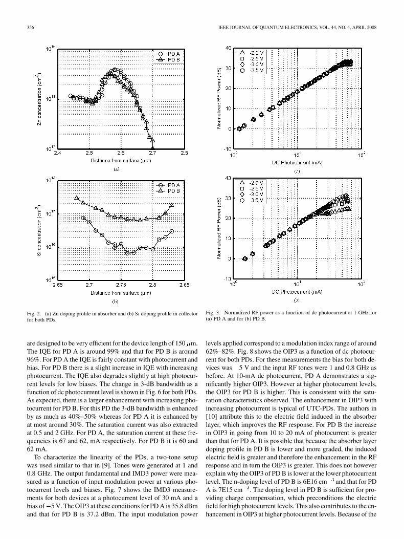
Of particular interest in understanding the device perfor-mance are the doping profiles in the absorber and collectorlayers. Zn is used for p-doping and Si is used for n-doping.The Zn and Si concentration in the structures were measuredby secondary ion mass spectroscopy. The doping profiles areshown in Fig. 2. The absorber p-doping level was intended tobe greater than 2E18 cm . Because of the high diffusivity ofZn at growth temperatures, the grading in the doping profilecan vary. For PD B, the peak Zn concentration in the absorberis 25% lower than that for PD A and the profile is more graded(high to low) toward the absorber/collector interface. Thesecharacteristics should result in a higher induced electric field inthe absorber region of PD B and therefore a larger enhancement
Fig. 1. Cross section SEM image of PD structure.
in the output response. The Si concentration in the collector ofPD A is 7E15 cm and that for PD B is 6E16 cm , nearly anorder of magnitude higher. The latter is adequate for providingcharge compensation. Devices were fabricated with variousgeometries. The results that follow are for devices that are10 m wide and 150 m long.
III. RESULTS AND DISCUSSION
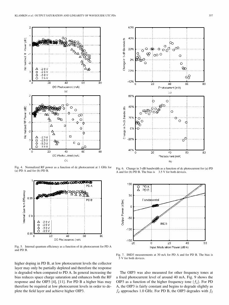
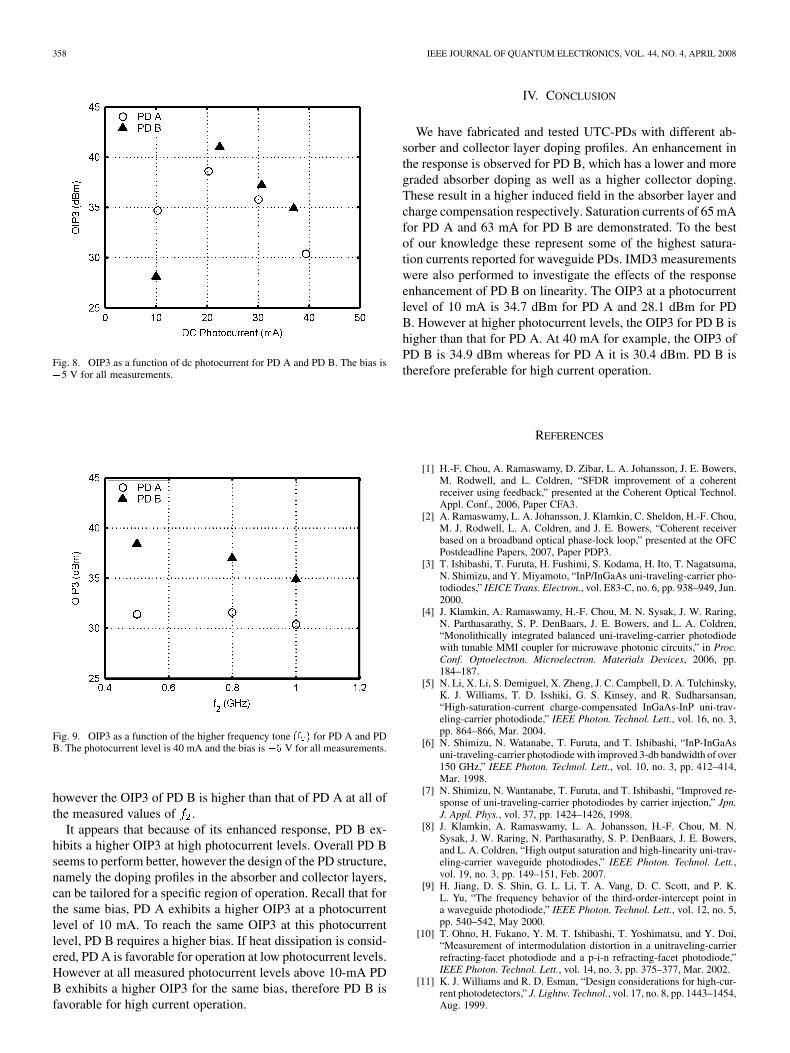
The electrical frequency responses of the UTC-PDs weremeasured at various biases for photocurrent levels up to around70 mA. Fig. 3 shows the RF power as a function of dc pho-tocurrent at 1 GHz for both devices. The data is normalized to0 dB. For these measurements the modulation depth was 50%.The saturation characteristics of PD B vary with bias more sothan those of PD A. The saturation current, defined here as thephotocurrent level where the RF response is compressed by1 dB, is around 65 mA for PD A and around 63 mA for PD B fora bias of 3.5 V. Fig. 4 shows the RF power normalized to anideal line with a slope of 20 dB/decade. For PD A, the responseis fairly constant with increasing photocurrent until the onsetof saturation. For PD B, there is a significant enhancement inthe response with increasing photocurrent. This enhancementis due in part to a small field induced in the absorber at highphotocurrent levels. The p-doping in the absorber of PD B islower and more graded so this field should be greater in thisdevice. The enhancement is also due to the higher n-dopingin the collector of PD B. This doping provides some chargecompensation and preconditions the electric field for operationat high photocurrent levels. Because the device areas are large,the 3-dB bandwidth is RC-limited. Therefore, any enhancementin the response should be attributed more so to improvementsin the field distribution in the depletion region or the devicecapacitance rather than improvements in carrier transit time.For low biases the RF response of PD B saturates at much lowerphotocurrent levels than that of PD A. For example, at a bias of
2 V the saturation current of PD B is less than 20 mA whereasfor PD A it is greater than 40 mA. This is due to the fact thatthe doping in the collector layer of PD B is significantly higher.As such a higher bias is required to deplete the collector layerand optimize the field profile.
The internal quantum efficiency (IQE) was also measured forboth PDs and the results are shown in Fig. 5. The PD structures
356 IEEE JOURNAL OF QUANTUM ELECTRONICS, VOL. 44, NO. 4, APRIL 2008
Fig. 2. (a) Zn doping profile in absorber and (b) Si doping profile in collectorfor both PDs.
are designed to be very efficient for the device length of 150 m.The IQE for PD A is around 99% and that for PD B is around96%. For PD A the IQE is fairly constant with photocurrent andbias. For PD B there is a slight increase in IQE with increasingphotocurrent. The IQE also degrades slightly at high photocur-rent levels for low biases. The change in 3-dB bandwidth as afunction of dc photocurrent level is shown in Fig. 6 for both PDs.As expected, there is a larger enhancement with increasing pho-tocurrent for PD B. For this PD the 3-dB bandwidth is enhancedby as much as 40%–50% whereas for PD A it is enhanced byat most around 30%. The saturation current was also extractedat 0.5 and 2 GHz. For PD A, the saturation current at these fre-quencies is 67 and 62, mA respectively. For PD B it is 60 and62 mA.
To characterize the linearity of the PDs, a two-tone setupwas used similar to that in [9]. Tones were generated at 1 and0.8 GHz. The output fundamental and IMD3 power were mea-sured as a function of input modulation power at various pho-tocurrent levels and biases. Fig. 7 shows the IMD3 measure-ments for both devices at a photocurrent level of 30 mA and abias of 5 V. The OIP3 at these conditions for PD A is 35.8 dBmand that for PD B is 37.2 dBm. The input modulation power
Fig. 3. Normalized RF power as a function of dc photocurrent at 1 GHz for(a) PD A and for (b) PD B.
levels applied correspond to a modulation index range of around62%–82%. Fig. 8 shows the OIP3 as a function of dc photocur-rent for both PDs. For these measurements the bias for both de-vices was 5 V and the input RF tones were 1 and 0.8 GHz asbefore. At 10-mA dc photocurrent, PD A demonstrates a sig-nificantly higher OIP3. However at higher photocurrent levels,the OIP3 for PD B is higher. This is consistent with the satu-ration characteristics observed. The enhancement in OIP3 withincreasing photocurrent is typical of UTC-PDs. The authors in[10] attribute this to the electric field induced in the absorberlayer, which improves the RF response. For PD B the increasein OIP3 in going from 10 to 20 mA of photocurrent is greaterthan that for PD A. It is possible that because the absorber layerdoping profile in PD B is lower and more graded, the inducedelectric field is greater and therefore the enhancement in the RFresponse and in turn the OIP3 is greater. This does not howeverexplain why the OIP3 of PD B is lower at the lower photocurrentlevel. The n-doping level of PD B is 6E16 cm and that for PDA is 7E15 cm . The doping level in PD B is sufficient for pro-viding charge compensation, which preconditions the electricfield for high photocurrent levels. This also contributes to the en-hancement in OIP3 at higher photocurrent levels. Because of the
KLAMKIN et al.: OUTPUT SATURATION AND LINEARITY OF WAVEGUIDE UTC PDs 357
Fig. 4. Normalized RF power as a function of dc photocurrent at 1 GHz for(a) PD A and for (b) PD B.
Fig. 5. Internal quantum efficiency as a function of dc photocurrent for PD Aand PD B.
higher doping in PD B, at low photocurrent levels the collectorlayer may only be partially depleted and therefore the responseis degraded when compared to PD A. In general increasing thebias reduces space charge saturation and enhances both the RFresponse and the OIP3 [4], [11]. For PD B a higher bias maytherefore be required at low photocurrent levels in order to de-plete the field layer and achieve higher OIP3.
Fig. 6. Change in 3-dB bandwidth as a function of dc photocurrent for (a) PDA and for (b) PD B. The bias is �3.5 V for both devices.
Fig. 7. IMD3 measurements at 30 mA for PD A and for PD B. The bias is�5 V for both devices.
The OIP3 was also measured for other frequency tones ata fixed photocurrent level of around 40 mA. Fig. 9 shows theOIP3 as a function of the higher frequency tone . For PDA, the OIP3 is fairly constant and begins to degrade slightly as
approaches 1.0 GHz. For PD B, the OIP3 degrades with
358 IEEE JOURNAL OF QUANTUM ELECTRONICS, VOL. 44, NO. 4, APRIL 2008
Fig. 8. OIP3 as a function of dc photocurrent for PD A and PD B. The bias is�5 V for all measurements.
Fig. 9. OIP3 as a function of the higher frequency tone �� � for PD A and PDB. The photocurrent level is 40 mA and the bias is �� V for all measurements.
however the OIP3 of PD B is higher than that of PD A at all ofthe measured values of .
It appears that because of its enhanced response, PD B ex-hibits a higher OIP3 at high photocurrent levels. Overall PD Bseems to perform better, however the design of the PD structure,namely the doping profiles in the absorber and collector layers,can be tailored for a specific region of operation. Recall that forthe same bias, PD A exhibits a higher OIP3 at a photocurrentlevel of 10 mA. To reach the same OIP3 at this photocurrentlevel, PD B requires a higher bias. If heat dissipation is consid-ered, PD A is favorable for operation at low photocurrent levels.However at all measured photocurrent levels above 10-mA PDB exhibits a higher OIP3 for the same bias, therefore PD B isfavorable for high current operation.
IV. CONCLUSION
We have fabricated and tested UTC-PDs with different ab-sorber and collector layer doping profiles. An enhancement inthe response is observed for PD B, which has a lower and moregraded absorber doping as well as a higher collector doping.These result in a higher induced field in the absorber layer andcharge compensation respectively. Saturation currents of 65 mAfor PD A and 63 mA for PD B are demonstrated. To the bestof our knowledge these represent some of the highest satura-tion currents reported for waveguide PDs. IMD3 measurementswere also performed to investigate the effects of the responseenhancement of PD B on linearity. The OIP3 at a photocurrentlevel of 10 mA is 34.7 dBm for PD A and 28.1 dBm for PDB. However at higher photocurrent levels, the OIP3 for PD B ishigher than that for PD A. At 40 mA for example, the OIP3 ofPD B is 34.9 dBm whereas for PD A it is 30.4 dBm. PD B istherefore preferable for high current operation.
REFERENCES
[1] H.-F. Chou, A. Ramaswamy, D. Zibar, L. A. Johansson, J. E. Bowers,M. Rodwell, and L. Coldren, “SFDR improvement of a coherentreceiver using feedback,” presented at the Coherent Optical Technol.Appl. Conf., 2006, Paper CFA3.
[2] A. Ramaswamy, L. A. Johansson, J. Klamkin, C. Sheldon, H.-F. Chou,M. J. Rodwell, L. A. Coldren, and J. E. Bowers, “Coherent receiverbased on a broadband optical phase-lock loop,” presented at the OFCPostdeadline Papers, 2007, Paper PDP3.
[3] T. Ishibashi, T. Furuta, H. Fushimi, S. Kodama, H. Ito, T. Nagatsuma,N. Shimizu, and Y. Miyamoto, “InP/InGaAs uni-traveling-carrier pho-todiodes,” IEICE Trans. Electron., vol. E83-C, no. 6, pp. 938–949, Jun.2000.
[4] J. Klamkin, A. Ramaswamy, H.-F. Chou, M. N. Sysak, J. W. Raring,N. Parthasarathy, S. P. DenBaars, J. E. Bowers, and L. A. Coldren,“Monolithically integrated balanced uni-traveling-carrier photodiodewith tunable MMI coupler for microwave photonic circuits,” in Proc.Conf. Optoelectron. Microelectron. Materials Devices, 2006, pp.184–187.
[5] N. Li, X. Li, S. Demiguel, X. Zheng, J. C. Campbell, D. A. Tulchinsky,K. J. Williams, T. D. Isshiki, G. S. Kinsey, and R. Sudharsansan,“High-saturation-current charge-compensated InGaAs-InP uni-trav-eling-carrier photodiode,” IEEE Photon. Technol. Lett., vol. 16, no. 3,pp. 864–866, Mar. 2004.
[6] N. Shimizu, N. Watanabe, T. Furuta, and T. Ishibashi, “InP-InGaAsuni-traveling-carrier photodiode with improved 3-db bandwidth of over150 GHz,” IEEE Photon. Technol. Lett., vol. 10, no. 3, pp. 412–414,Mar. 1998.
[7] N. Shimizu, N. Wantanabe, T. Furuta, and T. Ishibashi, “Improved re-sponse of uni-traveling-carrier photodiodes by carrier injection,” Jpn.J. Appl. Phys., vol. 37, pp. 1424–1426, 1998.
[8] J. Klamkin, A. Ramaswamy, L. A. Johansson, H.-F. Chou, M. N.Sysak, J. W. Raring, N. Parthasarathy, S. P. DenBaars, J. E. Bowers,and L. A. Coldren, “High output saturation and high-linearity uni-trav-eling-carrier waveguide photodiodes,” IEEE Photon. Technol. Lett.,vol. 19, no. 3, pp. 149–151, Feb. 2007.
[9] H. Jiang, D. S. Shin, G. L. Li, T. A. Vang, D. C. Scott, and P. K.L. Yu, “The frequency behavior of the third-order-intercept point ina waveguide photodiode,” IEEE Photon. Technol. Lett., vol. 12, no. 5,pp. 540–542, May 2000.
[10] T. Ohno, H. Fukano, Y. M. T. Ishibashi, T. Yoshimatsu, and Y. Doi,“Measurement of intermodulation distortion in a unitraveling-carrierrefracting-facet photodiode and a p-i-n refracting-facet photodiode,”IEEE Photon. Technol. Lett., vol. 14, no. 3, pp. 375–377, Mar. 2002.
[11] K. J. Williams and R. D. Esman, “Design considerations for high-cur-rent photodetectors,” J. Lightw. Technol., vol. 17, no. 8, pp. 1443–1454,Aug. 1999.
KLAMKIN et al.: OUTPUT SATURATION AND LINEARITY OF WAVEGUIDE UTC PDs 359
Jonathan Klamkin (S’04) received the B.S. degreein electrical and computer engineering from CornellUniversity, Ithaca, NY, in 2002, and the M.S. degreein electrical and computer engineering from the Uni-versity of California, Santa Barbara (UCSB) in 2004,where he is currently working toward the Ph.D. de-gree in materials.
His research interests include the design, epi-taxial growth, fabrication, and characterization ofwidely-tunable semiconductor lasers, photodetec-tors, optical intensity and phase modulators, compact
couplers, and semiconductor optical amplifiers for InP-based photonic inte-grated circuits. Currently his efforts are focused on novel coherent integratedreceivers for highly linear microwave photonic links.
Yu-Chia Chang received the B.S. degree in electricalengineering and the M.S. degree in electrooptical en-gineering from National Taiwan University, Taipei,Taiwan, R.O.C., in 1997 and 1999, respectively.He is currently working toward the Ph.D. degree inelectrical and computer engineering, University ofCalifornia, Santa Barbara (UCSB).
He worked for BenQ Inc., Taiwan, R.O.C., in1999–2001 and National Taiwan University in2001–2002. His current research interests are the de-sign, growth, and characterization of high-efficiency
high-speed vertical-cavity surface-emitting lasers for optical interconnectapplications.
Anand Ramaswamy (S’06) received the B.S.degree in electrical engineering with a minor inphysics from the University of Southern California,Los Angeles, 2005 and the M.S. degree in electricalengineering from the University of California, SantaBarbara, in 2007, respectively, where he is currentlyworking towards the Ph.D. degree under ProfessorJohn E. Bowers.
His research interests lie in coherent communi-cation systems and non-linear mechanisms in highpower photodetectors.
Leif. A Johansson received the Ph.D. degree in engineering from UniversityCollege London, U.K., in 2002.
He took up a postdoctoral position at the University of California at SantaBarbara in 2002. His current research interests include design and characteriza-tion of integrated photonic devices for analog and digital applications.
John E. Bowers (F’93) received the M.S. and Ph.D.degrees from Stanford University, Stanford, CA.
He is a Professor in the Department of ElectricalEngineering, and in the Technology ManagementProgram at the University of California, SantaBarbara. He is also CTO and cofounder of CalientNetworks. His research interests are primarilyconcerned with silicon photonics, optoelectronicdevices, optical switching and transparent opticalnetworks. He is cofounder of the Center for En-trepreneurship and Engineering Management, and
founder of Terabit Technology. He worked for AT&T Bell Laboratories andHoneywell before joining UCSB. He has published eight book chapters,400 journal papers, 600 conference papers and has received 49 patents.
Dr. Bowers is a Fellow of OSA and the American Physical Society, and a re-cipient of the IEEE LEOS William Streifer Award and the South Coast Businessand Technology Entrepreneur of the Year Award. He was an elected member ofthe IEEE LEOS Board of Governors, a LEOS Distinguished Lecturer, and VicePresident for Conferences for LEOS. He is a member of the National Academyof Engineering. He received the ACE Award for Most Promising Technologyfor the hybrid silicon laser in 2007.
Steven P. DenBaars (F’05) is a Professor of mate-rials and electrical and computer engineering, and theCo-Director of the Solid State Lighting and DisplayCenter, at the University of California, Santa Barbara.
His research areas are in MOCVD growth of wide-bandgap semiconductors (GaN-based) and their ap-plication to blue LEDs and laser and high-power elec-tronic devices.
Dr. DenBaars is the recipient of the MitsubishiChemical Endowed Chair in Solid State Lightingand Display.
Larry A. Coldren (F’82) received the Ph.D. degreein electrical engineering from Stanford University,Stanford, CA, in 1972.
He is the Fred Kavli Professor of Optoelectronicsand Sensors at the University of California, SantaBarbara. After 13 years in the research area at BellLaboratories, he joined UC-Santa Barbara in 1984where he now holds appointments in materials andelectrical and computer engineering, and is Directorof the Optoelectronics Technology Center. In 1990,he co-founded Optical Concepts, later acquired
as Gore Photonics, to develop novel VCSEL technology; and in 1998 heco-founded Agility Communications, recently acquired by JDSU, to developwidely-tunable integrated transmitters. He has authored or co-authored over800 papers, five book chapters, one textbook, and has been issued 61 patents.He has presented dozens of invited and plenary talks at major conferences.
Prof. Coldren is a Fellow of OSA, and IEE, U.K., the recipient of the 2004John Tyndall Award, and a member of the National Academy of Engineering.