Embed Size (px)
Citation preview
385 MHz BW IF Diversity Receiver Data Sheet AD6674
Rev. D Document Feedback Information furnished by Analog Devices is believed to be accurate and reliable. However, no responsibility is assumed by Analog Devices for its use, nor for any infringements of patents or other rights of third parties that may result from its use. Specifications subject to change without notice. No license is granted by implication or otherwise under any patent or patent rights of Analog Devices. Trademarks and registered trademarks are the property of their respective owners.
One Technology Way, P.O. Box 9106, Norwood, MA 02062-9106, U.S.A. Tel: 781.329.4700 ©2014–2018 Analog Devices, Inc. All rights reserved. Technical Support www.analog.com
FEATURES JESD204B (Subclass 1) coded serial digital outputs In band SFDR = 83 dBFS at 340 MHz (750 MSPS) In band SNR = 66.7 dBFS at 340 MHz (750 MSPS) 1.4 W total power per channel at 750 MSPS (default settings) Noise density = −153 dBFS/Hz at 750 MSPS 1.25 V, 2.5 V, and 3.3 V dc supply operation Flexible input range
AD6674-750 and AD6674-1000 1.46 V p-p to 1.94 V p-p (1.70 V p-p nominal)
AD6674-500 1.46 V p-p to 2.06 V p-p (2.06 V p-p nominal)
95 dB channel isolation/crosstalk Amplitude detect bits for efficient automatic gain control
(AGC) implementation Noise shaping requantizer (NSR) option for main receiver
function Variable dynamic range (VDR) option for digital
predistortion (DPD) function 2 integrated wideband digital processors per channel
12-bit numerically controlled oscillator (NCO), up to 4 cascaded half-band filters
Differential clock inputs Integer clock divide by 1, 2, 4, or 8 Energy saving power-down modes Flexible JESD204B lane configurations Small signal dither
APPLICATIONS Diversity multiband, multimode digital receivers
3G/4G, TD-SCDMA, W-CDMA, GSM, LTE, LTE-A DOCSIS 3.0 CMTS upstream receive paths HFC digital reverse path receivers
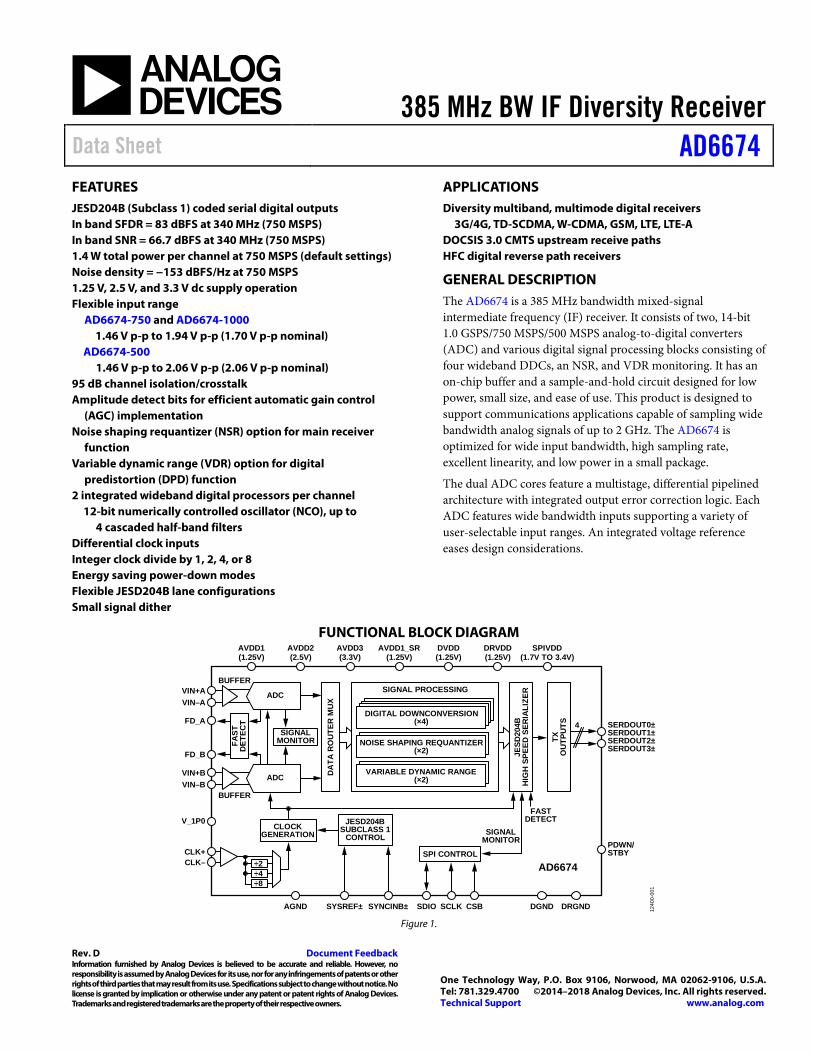
GENERAL DESCRIPTION The AD6674 is a 385 MHz bandwidth mixed-signal intermediate frequency (IF) receiver. It consists of two, 14-bit 1.0 GSPS/750 MSPS/500 MSPS analog-to-digital converters (ADC) and various digital signal processing blocks consisting of four wideband DDCs, an NSR, and VDR monitoring. It has an on-chip buffer and a sample-and-hold circuit designed for low power, small size, and ease of use. This product is designed to support communications applications capable of sampling wide bandwidth analog signals of up to 2 GHz. The AD6674 is optimized for wide input bandwidth, high sampling rate, excellent linearity, and low power in a small package.
The dual ADC cores feature a multistage, differential pipelined architecture with integrated output error correction logic. Each ADC features wide bandwidth inputs supporting a variety of user-selectable input ranges. An integrated voltage reference eases design considerations.
FUNCTIONAL BLOCK DIAGRAM 12
400-
001
VIN+AVIN–A
VIN+BVIN–B
AD6674
SERDOUT0±SERDOUT1±SERDOUT2±SERDOUT3±
SYSREF±
PDWN/STBY
SYNCINB±
FD_A
FD_B
BUFFER
BUFFER
JESD
204B
HIG
H S
PEED
SER
IALI
ZER
TXO
UTP
UTS
DA
TA R
OU
TER
MU
X
JESD204BSUBCLASS 1
CONTROL
FASTDETECT
SIGNALMONITOR
V_1P0
AGND DRGNDDGNDSDIO SCLK CSB
AVDD1(1.25V)
AVDD2(2.5V)
AVDD3(3.3V)
AVDD1_SR(1.25V)
DVDD(1.25V)
DRVDD(1.25V)
SPIVDD(1.7V TO 3.4V)
4
FAST
DET
ECT
SIGNALMONITOR
ADC
ADC
SPI CONTROLCLK+CLK– ÷2
÷4
CLOCKGENERATION
÷8
SIGNAL PROCESSING
DIGITAL DOWN CONVERSION(×4)DIGITAL DOWN CONVERSION
(×4)DIGITAL DOWN CONVERSION(×4)DIGITAL DOWNCONVERSION
(×4)
NOISE SHAPING REQUANTIZER(×2)NOISE SHAPING REQUANTIZER
(×2)
VARIABLE DYNAMIC RANGE(×2)VARIABLE DYNAMIC RANGE
(×2)
Figure 1.
AD6674 Data Sheet
Rev. D | Page 2 of 96
TABLE OF CONTENTS Features .............................................................................................. 1 Applications ....................................................................................... 1 General Description ......................................................................... 1 Functional Block Diagram .............................................................. 1 Revision History ............................................................................... 3 Product Highlights ........................................................................... 4 Specifications ..................................................................................... 5
DC Specifications ......................................................................... 5 AC Specifications .......................................................................... 6 Digital Specifications ................................................................... 8 Switching Specifications .............................................................. 9 Timing Specifications .................................................................. 9
Absolute Maximum Ratings .......................................................... 11 Thermal Characteristics ............................................................ 11 ESD Caution ................................................................................ 11
Pin Configuration and Function Descriptions ........................... 12 Typical Performance Characteristics ........................................... 14
AD6674-1000 .............................................................................. 14 AD6674-750 ................................................................................ 18 AD6674-500 ................................................................................ 22
Equivalent Circuits ......................................................................... 26 Theory of Operation ...................................................................... 28
ADC Architecture ...................................................................... 28 Analog Input Considerations .................................................... 28 Voltage Reference ....................................................................... 33 Clock Input Considerations ...................................................... 34 Power-Down/Standby Mode..................................................... 35 Temperature Diode .................................................................... 36
ADC Overrange and Fast Detect .................................................. 37 ADC Overrange (OR) ................................................................ 37 Fast Threshold Detection (FD_A and FD_B) ........................ 37
Signal Monitor ................................................................................ 38 SPORT over JESD204B .............................................................. 38
Digital Downconverter (DDC) ..................................................... 41 DDC I/Q Input Selection .......................................................... 41 DDC I/Q Output Selection ....................................................... 41 DDC General Description ........................................................ 41
Frequency Translation ................................................................... 47 General Description ................................................................... 47 DDC NCO + Mixer Loss and SFDR ........................................ 48
Numerically Controlled Oscillator .......................................... 48 FIR Filters ........................................................................................ 50
General Description ................................................................... 50 Half-Band Filters ........................................................................ 51 DDC Gain Stage ......................................................................... 52 DDC Complex to Real Conversion ......................................... 52 DDC Example Configurations ................................................. 53
Noise Shaping Requantizer (NSR) ............................................... 57 Decimating Half-Band Filter .................................................... 57 NSR Overview ............................................................................ 57
Variable Dynamic Range (VDR) .................................................. 60 VDR Real Mode.......................................................................... 61 VDR Complex Mode ................................................................. 61
Digital Outputs ............................................................................... 63 Introduction to JESD204B Interface ........................................ 63 JESD204B Overview .................................................................. 63 Functional Overview ................................................................. 64 JESD204B Link Establishment ................................................. 64 Physical Layer (Driver) Outputs .............................................. 66 JESD204B Tx Converter Mapping ........................................... 68 Configuring the JESD204B Link .............................................. 68
Multichip Synchronization ............................................................ 72 SYSREF± Setup/Hold Window Monitor ................................. 74
Test Modes ....................................................................................... 76 ADC Test Modes ........................................................................ 76 JESD204B Block Test Modes .................................................... 76
Serial Port Interface (SPI) .............................................................. 79 Configuration Using the SPI ..................................................... 79 Hardware Interface ..................................................................... 79 SPI Accessible Features .............................................................. 79
Memory Map .................................................................................. 80 Reading the Memory Map Register Table ............................... 80 Memory Map Register Table ..................................................... 81
Applications Information .............................................................. 95 Power Supply Recommendations ............................................. 95 Exposed Pad Thermal Heat Slug Recommendations ............ 95 AVDD1_SR (Pin 57) and AGND (Pin 56, Pin 60) ................ 95
Outline Dimensions ....................................................................... 96 Ordering Guide .......................................................................... 96
Data Sheet AD6674
Rev. D | Page 3 of 96
REVISION HISTORY 10/2018—Rev. C to Rev. D Change to Figure 102 ...................................................................... 42 Updated Outline Dimensions ........................................................ 96 Changes to Ordering Guide ........................................................... 96 8/2016—Rev. B to Rev. C Changes to Figure 1........................................................................... 1 Changes to Table 1 ............................................................................ 5 Changes to Table 5 ............................................................................ 9 Changes to Table 8 .......................................................................... 12 Added Figure 15; Renumbered Sequentially ............................... 15 Added Figure 34 .............................................................................. 19 Added Figure 53 .............................................................................. 23 Changes to Figure 72 ...................................................................... 27 Changes to Table 10 ........................................................................ 32 Changes to Input Clock Driver Section ....................................... 34 Changes to Clock Jitter Considerations Section ......................... 35 Changes to Setting Up the NCO FTW and POW Section ........ 48 Changes to JESD204B Overview Section ..................................... 63 Changes to Figure 123 Caption and Figure 124 .......................... 64 Changes to ADC Test Modes Section ........................................... 76 Added Datapath Soft Reset Section .............................................. 80 Changes to Table 45 ........................................................................ 81 Changes to Ordering Guide ........................................................... 96
4/2015—Rev. A to Rev. B Changed SPIVDD Range from 1.8 V to 3.3 V to 1.8 V to 3.4 V .................................................................. Throughout Changes to General Description Section ....................................... 4 Changes to Table 1 ............................................................................ 5 Changes to Table 3 ............................................................................ 8 Changes to Figure 14 ...................................................................... 15 Change to Figure 78 Caption ......................................................... 27 Changes to Table 10 ........................................................................ 29 Changes to Clock Jitter Considerations Section ......................... 32 Added Figure 92; Renumbered Sequentially ............................... 32 Changes to Digital Downconverter (DDC) Section ................... 37 Changes to Table 17 ........................................................................ 46 Changes to Table 23 ........................................................................ 49 Changes to Figure 108 .................................................................... 53 Changes to Figure 116 .................................................................... 56 Changes to Figure 117 and VDR Complex Mode Section ........ 57 Changes to Table 45 ........................................................................ 79 12/2014—Revision A: Initial Version
AD6674 Data Sheet
Rev. D | Page 4 of 96
The analog input and clock signals are differential inputs. The ADC data outputs are internally connected to four DDCs through a crossbar mux. Each DDC consists of up to five cascaded signal processing stages: a 12-bit frequency translator (NCO), and up to four half-band decimation filters.
Each ADC output is connected internally to an NSR block. The integrated NSR circuitry allows improved SNR performance in a smaller frequency band within the Nyquist bandwidth. The device supports two different output modes selectable via the SPI. With the NSR feature enabled, the outputs of the ADCs are processed such that the AD6674 supports enhanced SNR performance within a limited portion of the Nyquist bandwidth while maintaining a 9-bit output resolution. NSR is enabled by default on the AD6674.
Each ADC output is also connected internally to a VDR block. This optional mode allows full dynamic range for defined input signals. Inputs that are within a defined mask (based on DPD applications) are passed unaltered. Inputs that violate this defined mask result in the reduction of the output resolution.
With VDR, the dynamic range of the observation receiver is determined by a defined input frequency mask. For signals falling within the mask, the outputs are presented at the maximum resolution allowed. For signals exceeding defined power levels within this frequency mask, the output resolution is truncated. This mask is based on DPD applications and supports tunable real IF sampling, and zero IF or complex IF receive architectures.
Operation of the AD6674 between the DDC, NSR, and VDR modes is selectable via SPI-programmable profiles.
In addition to the DDC blocks, the AD6674 has several functions that simplify the AGC function in a communications receiver. The programmable threshold detector allows monitoring of the incoming signal power using the fast detect control bits in Register 0x245 of the ADC. If the input signal level exceeds the programmable threshold, the fast detect
indicator goes high. Because this threshold indicator has low latency, the user can quickly turn down the system gain to avoid an overrange condition at the ADC input. Besides the fast detect outputs, the AD6674 also offers signal monitoring capability. The signal monitoring block provides additional information about the signal being digitized by the ADC.
Users can configure the Subclasss 1 JESD204B-based high speed serialized output in a variety of two-lane and four-lane configurations, depending on the DDC configuration and the acceptable lane rate of the receiving logic device. Multidevice synchronization is supported through the SYSREF± and SYNCINB± input pins.
The AD6674 has flexible power-down options that allow signifi-cant power savings when desired. All of these features can be programmed using a 1.8 V capable 3-wire serial port interface (SPI).
The AD6674 is available in a Pb-free, 64-lead LFCSP, specified over the −40°C to +85°C industrial temperature range. This product is protected by a U.S. patent.
PRODUCT HIGHLIGHTS 1. Wide full power bandwidth supports IF sampling of signals
up to 2 GHz. 2. Buffered inputs with programmable input termination
eases filter design and implementation. 3. Four integrated wideband decimation filters and
numerically controlled oscillator (NCO) blocks supporting multiband receivers.
4. Flexible SPI controls various product features and functions to meet specific system requirements.
5. Programmable fast overrange detection and signal monitoring.
6. Programmable fast overrange detection. 7. 9 mm × 9 mm 64-lead LFCSP.
Data Sheet AD6674
Rev. D | Page 5 of 96
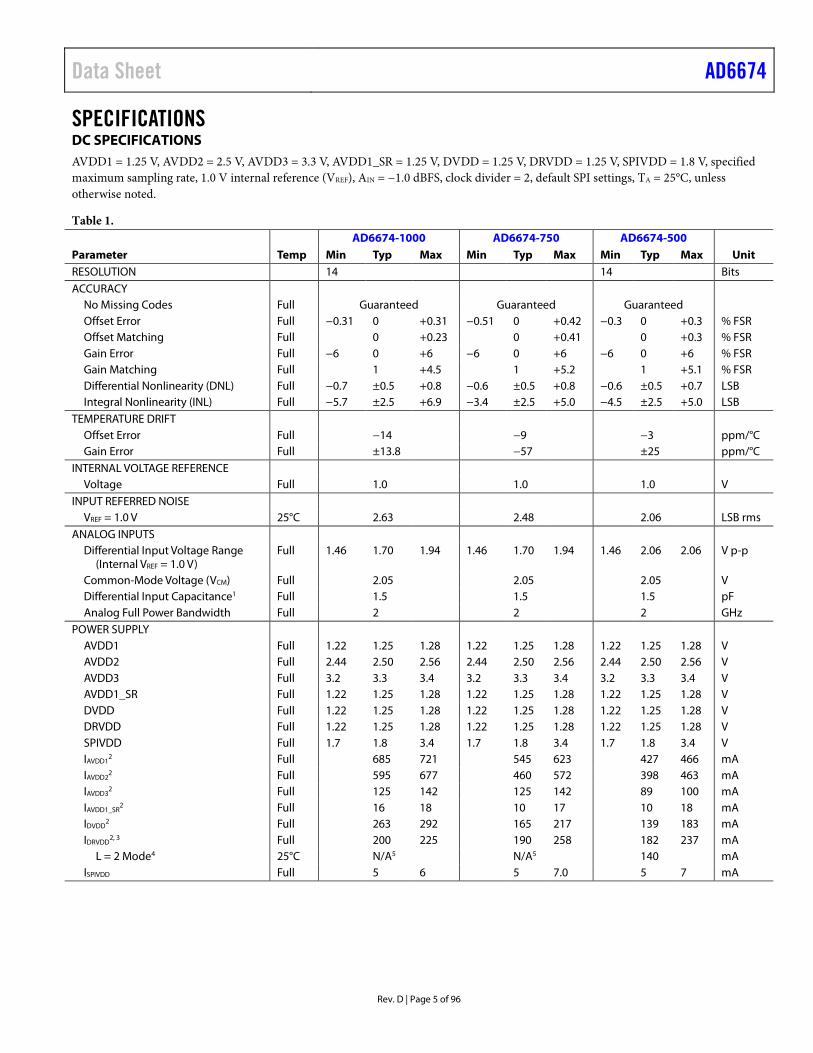
SPECIFICATIONS DC SPECIFICATIONS AVDD1 = 1.25 V, AVDD2 = 2.5 V, AVDD3 = 3.3 V, AVDD1_SR = 1.25 V, DVDD = 1.25 V, DRVDD = 1.25 V, SPIVDD = 1.8 V, specified maximum sampling rate, 1.0 V internal reference (VREF), AIN = −1.0 dBFS, clock divider = 2, default SPI settings, TA = 25°C, unless otherwise noted.
Table 1.
Parameter Temp AD6674-1000 AD6674-750 AD6674-500
Unit Min Typ Max Min Typ Max Min Typ Max RESOLUTION 14 14 Bits ACCURACY
No Missing Codes Full Guaranteed Guaranteed Guaranteed Offset Error Full −0.31 0 +0.31 −0.51 0 +0.42 −0.3 0 +0.3 % FSR Offset Matching Full 0 +0.23 0 +0.41 0 +0.3 % FSR Gain Error Full −6 0 +6 −6 0 +6 −6 0 +6 % FSR Gain Matching Full 1 +4.5 1 +5.2 1 +5.1 % FSR Differential Nonlinearity (DNL) Full −0.7 ±0.5 +0.8 −0.6 ±0.5 +0.8 −0.6 ±0.5 +0.7 LSB Integral Nonlinearity (INL) Full −5.7 ±2.5 +6.9 −3.4 ±2.5 +5.0 −4.5 ±2.5 +5.0 LSB
TEMPERATURE DRIFT Offset Error Full −14 −9 −3 ppm/°C Gain Error Full ±13.8 −57 ±25 ppm/°C
INTERNAL VOLTAGE REFERENCE Voltage Full 1.0 1.0 1.0 V
INPUT REFERRED NOISE VREF = 1.0 V 25°C 2.63 2.48 2.06 LSB rms
ANALOG INPUTS Differential Input Voltage Range
(Internal VREF = 1.0 V) Full 1.46 1.70 1.94 1.46 1.70 1.94 1.46 2.06 2.06 V p-p
Common-Mode Voltage (VCM) Full 2.05 2.05 2.05 V Differential Input Capacitance1 Full 1.5 1.5 1.5 pF Analog Full Power Bandwidth Full 2 2 2 GHz
POWER SUPPLY AVDD1 Full 1.22 1.25 1.28 1.22 1.25 1.28 1.22 1.25 1.28 V AVDD2 Full 2.44 2.50 2.56 2.44 2.50 2.56 2.44 2.50 2.56 V AVDD3 Full 3.2 3.3 3.4 3.2 3.3 3.4 3.2 3.3 3.4 V AVDD1_SR Full 1.22 1.25 1.28 1.22 1.25 1.28 1.22 1.25 1.28 V DVDD Full 1.22 1.25 1.28 1.22 1.25 1.28 1.22 1.25 1.28 V DRVDD Full 1.22 1.25 1.28 1.22 1.25 1.28 1.22 1.25 1.28 V SPIVDD Full 1.7 1.8 3.4 1.7 1.8 3.4 1.7 1.8 3.4 V IAVDD1
2 Full 685 721 545 623 427 466 mA IAVDD2
2 Full 595 677 460 572 398 463 mA IAVDD3
2 Full 125 142 125 142 89 100 mA IAVDD1_SR
2 Full 16 18 10 17 10 18 mA IDVDD
2 Full 263 292 165 217 139 183 mA IDRVDD
2, 3 Full 200 225 190 258 182 237 mA L = 2 Mode4 25°C N/A5 N/A5 140 mA
ISPIVDD Full 5 6 5 7.0 5 7 mA
AD6674 Data Sheet
Rev. D | Page 6 of 96
Parameter Temp AD6674-1000 AD6674-750 AD6674-500
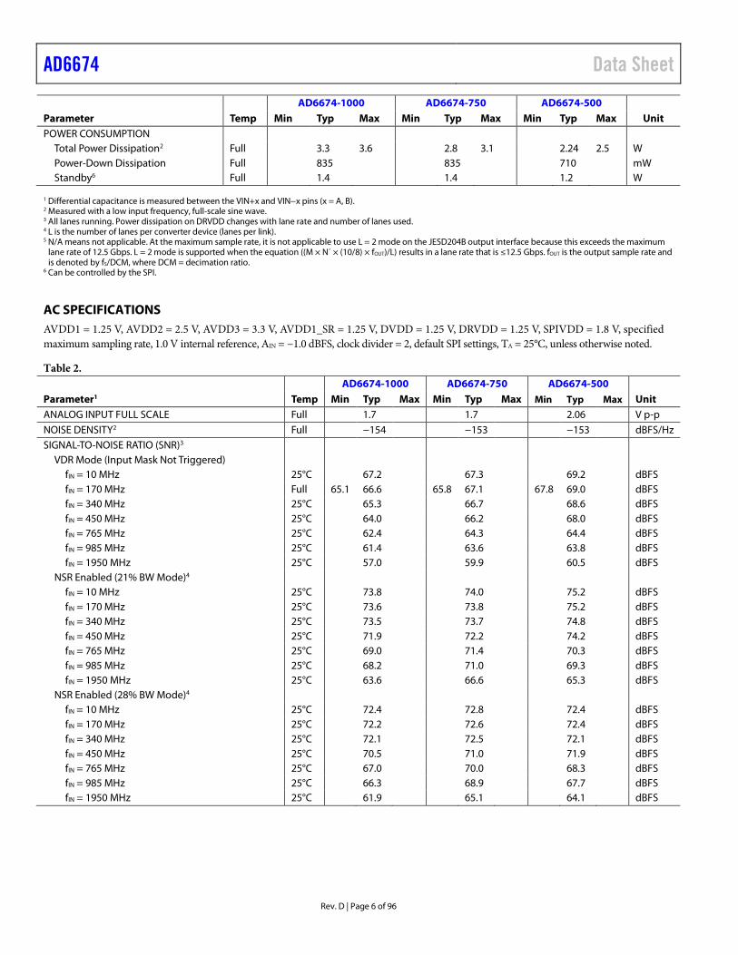
Unit Min Typ Max Min Typ Max Min Typ Max POWER CONSUMPTION
Total Power Dissipation2 Full 3.3 3.6 2.8 3.1 2.24 2.5 W Power-Down Dissipation Full 835 835 710 mW Standby6 Full 1.4 1.4 1.2 W
1 Differential capacitance is measured between the VIN+x and VIN−x pins (x = A, B). 2 Measured with a low input frequency, full-scale sine wave. 3 All lanes running. Power dissipation on DRVDD changes with lane rate and number of lanes used. 4 L is the number of lanes per converter device (lanes per link). 5 N/A means not applicable. At the maximum sample rate, it is not applicable to use L = 2 mode on the JESD204B output interface because this exceeds the maximum
lane rate of 12.5 Gbps. L = 2 mode is supported when the equation ((M × N΄ × (10/8) × fOUT)/L) results in a lane rate that is ≤12.5 Gbps. fOUT is the output sample rate and is denoted by fS/DCM, where DCM = decimation ratio.
6 Can be controlled by the SPI.
AC SPECIFICATIONS AVDD1 = 1.25 V, AVDD2 = 2.5 V, AVDD3 = 3.3 V, AVDD1_SR = 1.25 V, DVDD = 1.25 V, DRVDD = 1.25 V, SPIVDD = 1.8 V, specified maximum sampling rate, 1.0 V internal reference, AIN = −1.0 dBFS, clock divider = 2, default SPI settings, TA = 25°C, unless otherwise noted.
Table 2.
Parameter1 Temp AD6674-1000 AD6674-750 AD6674-500
Unit Min Typ Max Min Typ Max Min Typ Max
ANALOG INPUT FULL SCALE Full 1.7 1.7 2.06 V p-p NOISE DENSITY2 Full −154 −153 −153 dBFS/Hz SIGNAL-TO-NOISE RATIO (SNR)3
VDR Mode (Input Mask Not Triggered) fIN = 10 MHz 25°C 67.2 67.3 69.2 dBFS fIN = 170 MHz Full 65.1 66.6 65.8 67.1 67.8 69.0 dBFS fIN = 340 MHz 25°C 65.3 66.7 68.6 dBFS fIN = 450 MHz 25°C 64.0 66.2 68.0 dBFS fIN = 765 MHz 25°C 62.4 64.3 64.4 dBFS fIN = 985 MHz 25°C 61.4 63.6 63.8 dBFS fIN = 1950 MHz 25°C 57.0 59.9 60.5 dBFS
NSR Enabled (21% BW Mode)4 fIN = 10 MHz 25°C 73.8 74.0 75.2 dBFS fIN = 170 MHz 25°C 73.6 73.8 75.2 dBFS fIN = 340 MHz 25°C 73.5 73.7 74.8 dBFS fIN = 450 MHz 25°C 71.9 72.2 74.2 dBFS fIN = 765 MHz 25°C 69.0 71.4 70.3 dBFS fIN = 985 MHz 25°C 68.2 71.0 69.3 dBFS fIN = 1950 MHz 25°C 63.6 66.6 65.3 dBFS
NSR Enabled (28% BW Mode)4 fIN = 10 MHz 25°C 72.4 72.8 72.4 dBFS fIN = 170 MHz 25°C 72.2 72.6 72.4 dBFS fIN = 340 MHz 25°C 72.1 72.5 72.1 dBFS fIN = 450 MHz 25°C 70.5 71.0 71.9 dBFS fIN = 765 MHz 25°C 67.0 70.0 68.3 dBFS fIN = 985 MHz 25°C 66.3 68.9 67.7 dBFS fIN = 1950 MHz 25°C 61.9 65.1 64.1 dBFS
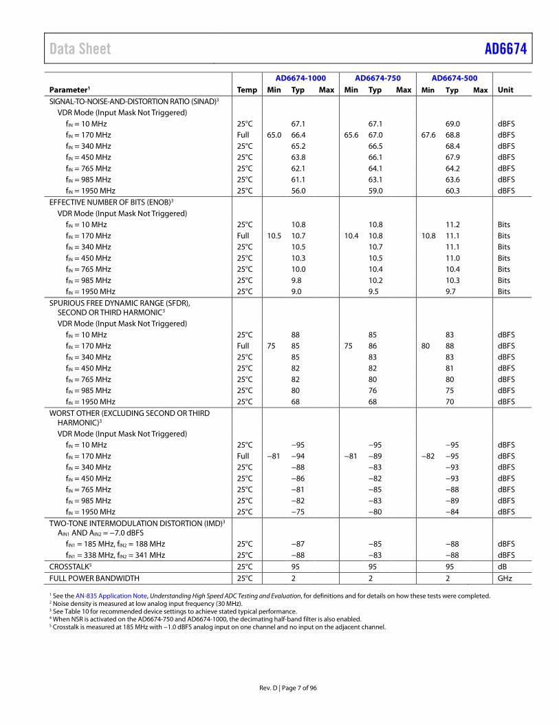
Data Sheet AD6674
Rev. D | Page 7 of 96
Parameter1 Temp AD6674-1000 AD6674-750 AD6674-500
Unit Min Typ Max Min Typ Max Min Typ Max
SIGNAL-TO-NOISE-AND-DISTORTION RATIO (SINAD)3 VDR Mode (Input Mask Not Triggered)
fIN = 10 MHz 25°C 67.1 67.1 69.0 dBFS fIN = 170 MHz Full 65.0 66.4 65.6 67.0 67.6 68.8 dBFS fIN = 340 MHz 25°C 65.2 66.5 68.4 dBFS fIN = 450 MHz 25°C 63.8 66.1 67.9 dBFS fIN = 765 MHz 25°C 62.1 64.1 64.2 dBFS fIN = 985 MHz 25°C 61.1 63.1 63.6 dBFS fIN = 1950 MHz 25°C 56.0 59.0 60.3 dBFS
EFFECTIVE NUMBER OF BITS (ENOB)3 VDR Mode (Input Mask Not Triggered)
fIN = 10 MHz 25°C 10.8 10.8 11.2 Bits fIN = 170 MHz Full 10.5 10.7 10.4 10.8 10.8 11.1 Bits fIN = 340 MHz 25°C 10.5 10.7 11.1 Bits fIN = 450 MHz 25°C 10.3 10.5 11.0 Bits fIN = 765 MHz 25°C 10.0 10.4 10.4 Bits fIN = 985 MHz 25°C 9.8 10.2 10.3 Bits fIN = 1950 MHz 25°C 9.0 9.5 9.7 Bits
SPURIOUS FREE DYNAMIC RANGE (SFDR), SECOND OR THIRD HARMONIC3
VDR Mode (Input Mask Not Triggered) fIN = 10 MHz 25°C 88 85 83 dBFS fIN = 170 MHz Full 75 85 75 86 80 88 dBFS fIN = 340 MHz 25°C 85 83 83 dBFS fIN = 450 MHz 25°C 82 82 81 dBFS fIN = 765 MHz 25°C 82 80 80 dBFS fIN = 985 MHz 25°C 80 76 75 dBFS fIN = 1950 MHz 25°C 68 68 70 dBFS
WORST OTHER (EXCLUDING SECOND OR THIRD HARMONIC)3
VDR Mode (Input Mask Not Triggered) fIN = 10 MHz 25°C −95 −95 −95 dBFS fIN = 170 MHz Full −81 −94 −81 −89 −82 −95 dBFS fIN = 340 MHz 25°C −88 −83 −93 dBFS fIN = 450 MHz 25°C −86 −82 −93 dBFS fIN = 765 MHz 25°C −81 −85 −88 dBFS fIN = 985 MHz 25°C −82 −83 −89 dBFS fIN = 1950 MHz 25°C −75 −80 −84 dBFS
TWO-TONE INTERMODULATION DISTORTION (IMD)3 AIN1 AND AIN2 = −7.0 dBFS
fIN1 = 185 MHz, fIN2 = 188 MHz 25°C −87 −85 −88 dBFS fIN1 = 338 MHz, fIN2 = 341 MHz 25°C −88 −83 −88 dBFS
CROSSTALK5 25°C 95 95 95 dB FULL POWER BANDWIDTH 25°C 2 2 2 GHz 1 See the AN-835 Application Note, Understanding High Speed ADC Testing and Evaluation, for definitions and for details on how these tests were completed. 2 Noise density is measured at low analog input frequency (30 MHz). 3 See Table 10 for recommended device settings to achieve stated typical performance. 4 When NSR is activated on the AD6674-750 and AD6674-1000, the decimating half-band filter is also enabled. 5 Crosstalk is measured at 185 MHz with −1.0 dBFS analog input on one channel and no input on the adjacent channel.
AD6674 Data Sheet
Rev. D | Page 8 of 96
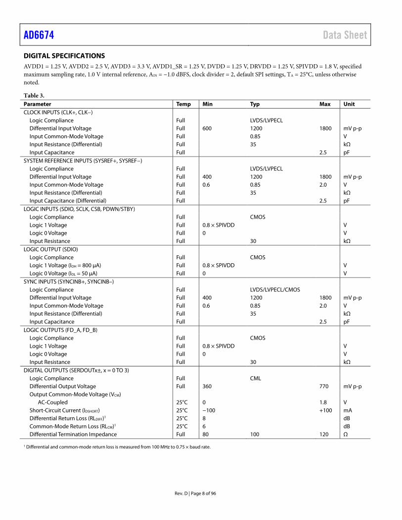
DIGITAL SPECIFICATIONS AVDD1 = 1.25 V, AVDD2 = 2.5 V, AVDD3 = 3.3 V, AVDD1_SR = 1.25 V, DVDD = 1.25 V, DRVDD = 1.25 V, SPIVDD = 1.8 V, specified maximum sampling rate, 1.0 V internal reference, AIN = −1.0 dBFS, clock divider = 2, default SPI settings, TA = 25°C, unless otherwise noted.
Table 3. Parameter Temp Min Typ Max Unit CLOCK INPUTS (CLK+, CLK−)
Logic Compliance Full LVDS/LVPECL Differential Input Voltage Full 600 1200 1800 mV p-p Input Common-Mode Voltage Full 0.85 V Input Resistance (Differential) Full 35 kΩ Input Capacitance Full 2.5 pF
SYSTEM REFERENCE INPUTS (SYSREF+, SYSREF−) Logic Compliance Full LVDS/LVPECL Differential Input Voltage Full 400 1200 1800 mV p-p Input Common-Mode Voltage Full 0.6 0.85 2.0 V Input Resistance (Differential) Full 35 kΩ Input Capacitance (Differential) Full 2.5 pF
LOGIC INPUTS (SDIO, SCLK, CSB, PDWN/STBY) Logic Compliance Full CMOS Logic 1 Voltage Full 0.8 × SPIVDD V Logic 0 Voltage Full 0 V Input Resistance Full 30 kΩ
LOGIC OUTPUT (SDIO) Logic Compliance Full CMOS Logic 1 Voltage (IOH = 800 µA) Full 0.8 × SPIVDD V Logic 0 Voltage (IOL = 50 µA) Full 0 V
SYNC INPUTS (SYNCINB+, SYNCINB–) Logic Compliance Full LVDS/LVPECL/CMOS Differential Input Voltage Full 400 1200 1800 mV p-p Input Common-Mode Voltage Full 0.6 0.85 2.0 V Input Resistance (Differential) Full 35 kΩ Input Capacitance Full 2.5 pF
LOGIC OUTPUTS (FD_A, FD_B) Logic Compliance Full CMOS Logic 1 Voltage Full 0.8 × SPIVDD V Logic 0 Voltage Full 0 V Input Resistance Full 30 kΩ
DIGITAL OUTPUTS (SERDOUTx±, x = 0 TO 3) Logic Compliance Full CML Differential Output Voltage Full 360 770 mV p-p Output Common-Mode Voltage (VCM)
AC-Coupled 25°C 0 1.8 V Short-Circuit Current (IDSHORT) 25°C −100 +100 mA Differential Return Loss (RLDIFF)1 25°C 8 dB Common-Mode Return Loss (RLCM)1 25°C 6 dB Differential Termination Impedance Full 80 100 120 Ω
1 Differential and common-mode return loss is measured from 100 MHz to 0.75 × baud rate.
Data Sheet AD6674
Rev. D | Page 9 of 96
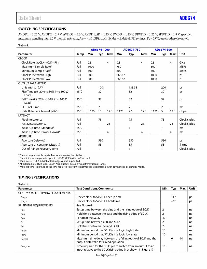
SWITCHING SPECIFICATIONS AVDD1 = 1.25 V, AVDD2 = 2.5 V, AVDD3 = 3.3 V, AVDD1_SR = 1.25 V, DVDD = 1.25 V, DRVDD = 1.25 V, SPIVDD = 1.8 V, specified maximum sampling rate, 1.0 V internal reference, AIN = −1.0 dBFS, clock divider = 2, default SPI settings, TA = 25°C, unless otherwise noted.
Table 4.
Parameter Temp AD6674-1000 AD6674-750 AD6674-500
Unit Min Typ Max Min Typ Max Min Typ Max CLOCK
Clock Rate (at CLK+/CLK− Pins) Full 0.3 4 0.3 4 0.3 4 GHz Maximum Sample Rate1 Full 1000 750 500 MSPS Minimum Sample Rate2 Full 300 300 300 MSPS Clock Pulse Width High Full 500 666.67 1000 ps Clock Pulse Width Low Full 500 666.67 1000 ps
OUTPUT PARAMETERS Unit Interval (UI)3 Full 100 133.33 200 ps Rise Time (tR) (20% to 80% into 100 Ω
Load) 25°C 32 32 32 ps
Fall Time (tF) (20% to 80% into 100 Ω Load)
25°C 32 32 32 ps
PLL Lock Time 25°C 2 2 2 ms Data Rate per Channel (NRZ)4 25°C 3.125 10 12.5 3.125 7.5 12.5 3.125 5 12.5 Gbps
LATENCY Pipeline Latency Full 75 75 75 Clock cycles Fast Detect Latency Full 28 28 28 Clock cycles Wake-Up Time (Standby)5 25°C 1 1 1 ms Wake-Up Time (Power-Down)5 25°C 4 4 4 ms
APERTURE Aperture Delay (tA) Full 530 530 530 ps Aperture Uncertainty (Jitter, tJ) Full 55 55 55 fs rms Out-of-Range Recovery Time Full 1 1 1 Clock cycles
1 The maximum sample rate is the clock rate after the divider. 2 The minimum sample rate operates at 300 MSPS with L = 2 or L = 1. 3 Baud rate = 1/UI. A subset of this range can be supported. 4 At full baud rate (12.5 Gbps), each ADC outputs data on two differential pair lanes. 5 Wake-up time is defined as the time required to return to normal operation from power-down mode or standby mode.
TIMING SPECIFICATIONS
Table 5. Parameter Test Conditions/Comments Min Typ Max Unit CLK± to SYSREF± TIMING REQUIREMENTS
tSU_SR Device clock to SYSREF± setup time 117 ps tH_SR Device clock to SYSREF± hold time −96 ps
SPI TIMING REQUIREMENTS See Figure 4 tDS Setup time between the data and the rising edge of SCLK 2 ns tDH Hold time between the data and the rising edge of SCLK 2 ns tCLK Period of the SCLK 40 ns tS Setup time between CSB and SCLK 2 ns tH Hold time between CSB and SCLK 2 ns tHIGH Minimum period that SCLK is in a logic high state 10 ns tLOW Minimum period that SCLK is in a logic low state 10 ns tACCESS Maximum time delay between the falling edge of SCLK and the
output data valid for a read operation 6 10 ns
tDIS_SDIO Time required for the SDIO pin to switch from an output to an input relative to the SCLK rising edge (not shown in Figure 4)
10 ns
AD6674 Data Sheet
Rev. D | Page 10 of 96
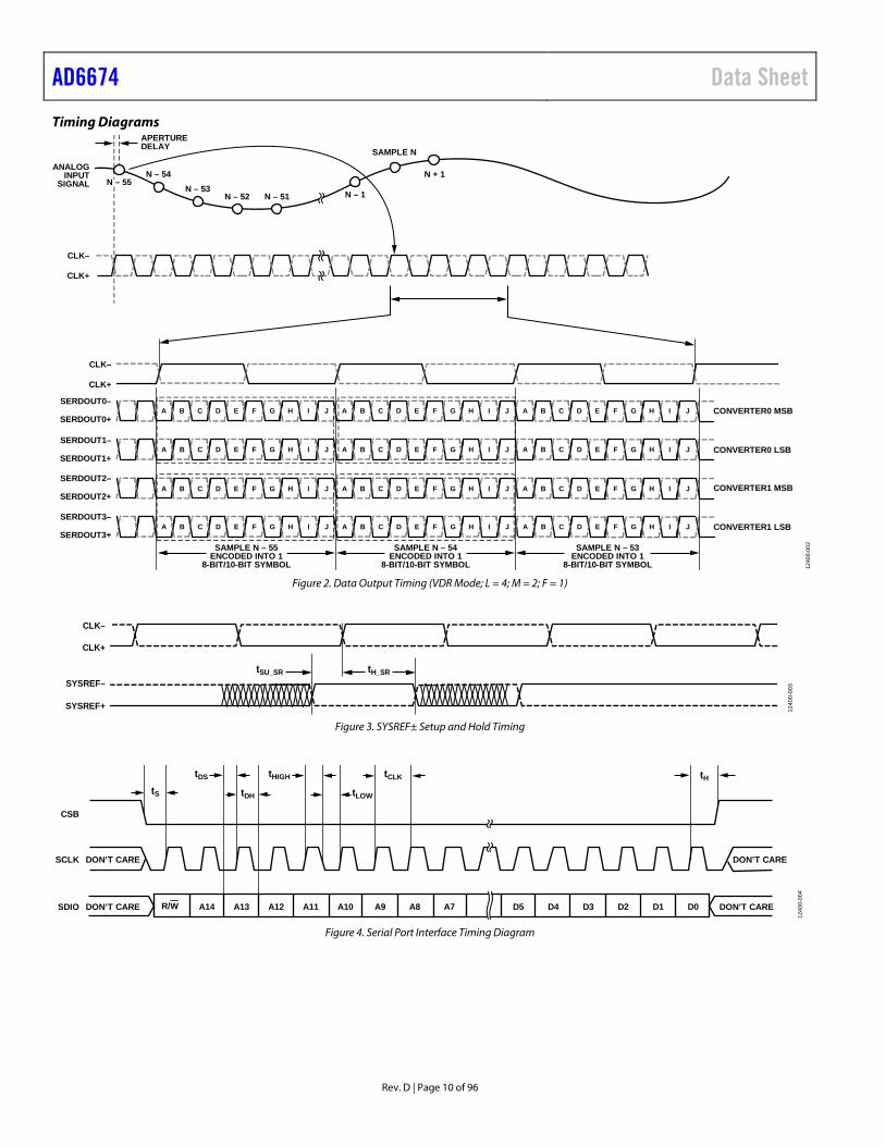
Timing Diagrams
SERDOUT0–
N – 54N – 53
N – 52 N – 51 N – 1
SAMPLE N
N + 1
APERTUREDELAY
N – 55
CLK+
CLK–
CLK+
CLK–
SERDOUT0+
SERDOUT1–
SERDOUT1+
SERDOUT2–
SERDOUT2+
SERDOUT3–
SERDOUT3+
A B C D E F G H I J A B C D E F G H I J A B C D E F G H I J
A B C D E F G H I J A B C D E F G H I J A B C D E F G H I J
A B C D E F G H I J A B C D E F G H I J A B C D E F G H I J
A B C D E F G H I J A B C D E F G H I J A B C D E F G H I J
CONVERTER0 MSB
CONVERTER0 LSB
CONVERTER1 MSB
CONVERTER1 LSB
ANALOGINPUT
SIGNAL
SAMPLE N – 55ENCODED INTO 1
8-BIT/10-BIT SYMBOL
SAMPLE N – 54ENCODED INTO 1
8-BIT/10-BIT SYMBOL
SAMPLE N – 53ENCODED INTO 1
8-BIT/10-BIT SYMBOL 1240
0-00
2
Figure 2. Data Output Timing (VDR Mode; L = 4; M = 2; F = 1)
CLK+
CLK–
SYSREF+
SYSREF–tSU_SR tH_SR
1240
0-00
3
Figure 3. SYSREF± Setup and Hold Timing
DON’T CARE
DON’T CAREDON’T CARE
DON’T CARE
SDIO
SCLK
tS tDH
tCLKtDS tH
R/W A14 A13 A12 A11 A10 A9 A8 A7 D5 D4 D3 D2 D1 D0
tLOW
tHIGH
CSB
1240
0-00
4
Figure 4. Serial Port Interface Timing Diagram
Data Sheet AD6674
Rev. D | Page 11 of 96
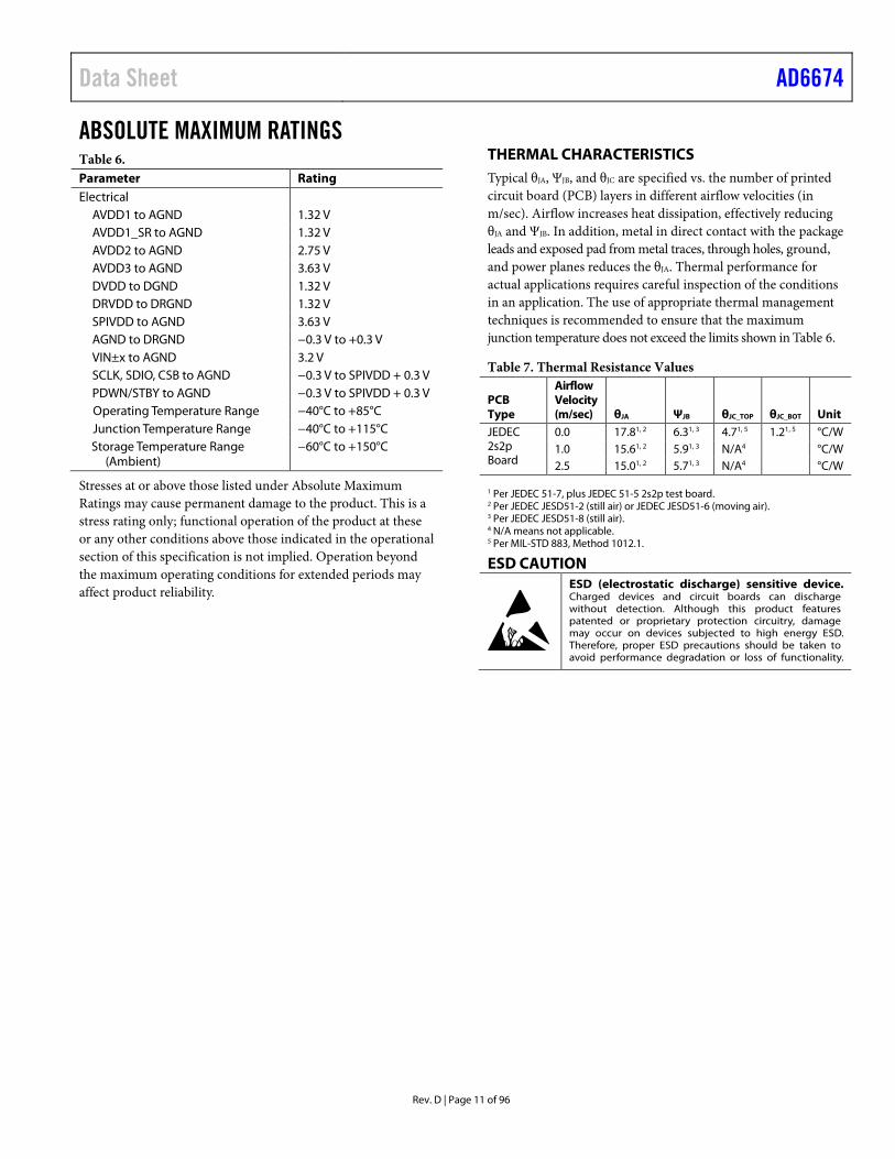
ABSOLUTE MAXIMUM RATINGS Table 6. Parameter Rating Electrical
AVDD1 to AGND 1.32 V AVDD1_SR to AGND 1.32 V AVDD2 to AGND 2.75 V AVDD3 to AGND 3.63 V DVDD to DGND 1.32 V DRVDD to DRGND 1.32 V SPIVDD to AGND 3.63 V AGND to DRGND −0.3 V to +0.3 V VIN±x to AGND 3.2 V SCLK, SDIO, CSB to AGND −0.3 V to SPIVDD + 0.3 V PDWN/STBY to AGND −0.3 V to SPIVDD + 0.3 V Operating Temperature Range −40°C to +85°C Junction Temperature Range −40°C to +115°C Storage Temperature Range
(Ambient) −60°C to +150°C
Stresses at or above those listed under Absolute Maximum Ratings may cause permanent damage to the product. This is a stress rating only; functional operation of the product at these or any other conditions above those indicated in the operational section of this specification is not implied. Operation beyond the maximum operating conditions for extended periods may affect product reliability.
THERMAL CHARACTERISTICS Typical θJA, ΨJB, and θJC are specified vs. the number of printed circuit board (PCB) layers in different airflow velocities (in m/sec). Airflow increases heat dissipation, effectively reducing θJA and ΨJB. In addition, metal in direct contact with the package leads and exposed pad from metal traces, through holes, ground, and power planes reduces the θJA. Thermal performance for actual applications requires careful inspection of the conditions in an application. The use of appropriate thermal management techniques is recommended to ensure that the maximum junction temperature does not exceed the limits shown in Table 6.
Table 7. Thermal Resistance Values
PCB Type
Airflow Velocity (m/sec) θJA ΨJB θJC_TOP θJC_BOT Unit
JEDEC 2s2p Board
0.0 17.81, 2 6.31, 3 4.71, 5 1.21, 5 °C/W 1.0 15.61, 2 5.91, 3 N/A4 °C/W 2.5 15.01, 2 5.71, 3 N/A4 °C/W
1 Per JEDEC 51-7, plus JEDEC 51-5 2s2p test board. 2 Per JEDEC JESD51-2 (still air) or JEDEC JESD51-6 (moving air). 3 Per JEDEC JESD51-8 (still air). 4 N/A means not applicable. 5 Per MIL-STD 883, Method 1012.1.
ESD CAUTION
AD6674 Data Sheet
Rev. D | Page 12 of 96
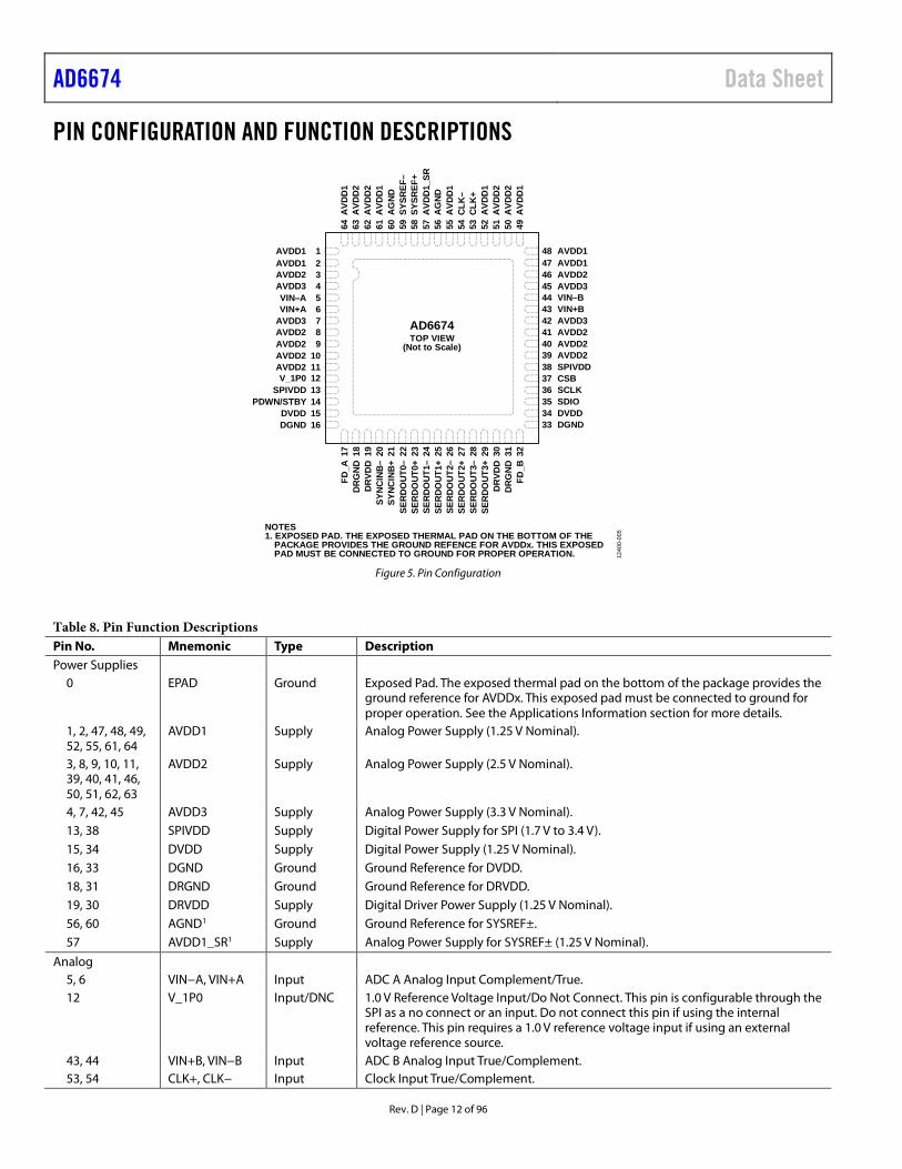
PIN CONFIGURATION AND FUNCTION DESCRIPTIONS
AD6674TOP VIEW
(Not to Scale)17 18 19 20 21 22 23 24 25 26 27 28 29 30 31 32
FD_A
DR
GN
DD
RVD
DSY
NC
INB
–SY
NC
INB
+SE
RD
OU
T0–
SER
DO
UT0
+SE
RD
OU
T1–
SER
DO
UT1
+SE
RD
OU
T2–
SER
DO
UT2
+SE
RD
OU
T3–
SER
DO
UT3
+D
RVD
DD
RG
ND
FD_B
64 63 62 61 60 59 58 57 56 55 54 53 52 51 50 49
AVD
D1
AVD
D2
AVD
D2
AVD
D1
AG
ND
SYSR
EF–
SYSR
EF+
AVD
D1_
SRA
GN
DA
VDD
1C
LK–
CLK
+A
VDD
1A
VDD
2A
VDD
2A
VDD
1
123456789
10111213141516
AVDD1AVDD1AVDD2AVDD3VIN–AVIN+A
AVDD3AVDD2AVDD2AVDD2AVDD2V_1P0
SPIVDDPDWN/STBY
DVDDDGND
AVDD1AVDD1AVDD2AVDD3VIN–BVIN+BAVDD3AVDD2AVDD2AVDD2SPIVDDCSBSCLKSDIODVDDDGND
48474645444342414039383736353433
NOTES1. EXPOSED PAD. THE EXPOSED THERMAL PAD ON THE BOTTOM OF THE
PACKAGE PROVIDES THE GROUND REFENCE FOR AVDDx. THIS EXPOSEDPAD MUST BE CONNECTED TO GROUND FOR PROPER OPERATION. 12
400-
005
Figure 5. Pin Configuration
Table 8. Pin Function Descriptions Pin No. Mnemonic Type Description Power Supplies
0 EPAD Ground Exposed Pad. The exposed thermal pad on the bottom of the package provides the ground reference for AVDDx. This exposed pad must be connected to ground for proper operation. See the Applications Information section for more details.
1, 2, 47, 48, 49, 52, 55, 61, 64
AVDD1 Supply Analog Power Supply (1.25 V Nominal).
3, 8, 9, 10, 11, 39, 40, 41, 46, 50, 51, 62, 63
AVDD2 Supply Analog Power Supply (2.5 V Nominal).
4, 7, 42, 45 AVDD3 Supply Analog Power Supply (3.3 V Nominal). 13, 38 SPIVDD Supply Digital Power Supply for SPI (1.7 V to 3.4 V). 15, 34 DVDD Supply Digital Power Supply (1.25 V Nominal). 16, 33 DGND Ground Ground Reference for DVDD. 18, 31 DRGND Ground Ground Reference for DRVDD. 19, 30 DRVDD Supply Digital Driver Power Supply (1.25 V Nominal). 56, 60 AGND1 Ground Ground Reference for SYSREF±. 57 AVDD1_SR1 Supply Analog Power Supply for SYSREF± (1.25 V Nominal).
Analog 5, 6 VIN−A, VIN+A Input ADC A Analog Input Complement/True. 12 V_1P0 Input/DNC 1.0 V Reference Voltage Input/Do Not Connect. This pin is configurable through the
SPI as a no connect or an input. Do not connect this pin if using the internal reference. This pin requires a 1.0 V reference voltage input if using an external voltage reference source.
43, 44 VIN+B, VIN−B Input ADC B Analog Input True/Complement. 53, 54 CLK+, CLK− Input Clock Input True/Complement.
Data Sheet AD6674
Rev. D | Page 13 of 96
Pin No. Mnemonic Type Description CMOS Outputs
17, 32 FD_A, FD_B Output Fast Detect Outputs for Channel A and Channel B. Digital Inputs
20, 21 SYNCINB−, SYNCINB+
Input Active Low JESD204B LVDS Sync Input True/Complement.
58, 59 SYSREF+, SYSREF−
Input Active Low JESD204B LVDS System Reference Input True/Complement.
Data Outputs 22, 23 SERDOUT0−,
SERDOUT0+ Output Lane 0 Output Data Complement/True.
24, 25 SERDOUT1−, SERDOUT1+
Output Lane 1 Output Data Complement/True.
26, 27 SERDOUT2−, SERDOUT2+
Output Lane 2 Output Data Complement/True.
28, 29 SERDOUT3−, SERDOUT3+
Output Lane 3 Output Data Complement/True.
Device Under Test (DUT) Controls
14 PDWN/STBY Input Power-Down Input (Active High). The operation of this pin depends on the SPI mode and can be configured as power-down or standby. This pin requires an external 10 kΩ pull-down resistor.
35 SDIO Input/Output SPI Serial Data Input/Output. 36 SCLK Input SPI Serial Clock. 37 CSB Input SPI Chip Select (Active Low).
1 To ensure proper ADC operation, connect AVDD1_SR and AGND separately from the AVDD1 and EPAD connection. For more information, see the Applications
Information section.
AD6674 Data Sheet
Rev. D | Page 14 of 96
TYPICAL PERFORMANCE CHARACTERISTICS AD6674-1000 AVDD1 = 1.25 V, AVDD1_SR = 1.25 V, AVDD2 = 2.5 V, AVDD3 = 3.3 V, DVDD = 1.25 V, DRVDD = 1.25 V, SPIVDD = 1.8 V, AIN = −1.0 dBFS, VDR mode (no violation of VDR mask), clock divider = 2, otherwise default SPI settings, TA = 25°C, 128k FFT sample, unless otherwise noted. See Table 10 for recommended settings.
–130
–110
–90
–70
–50
–30
–10
0 500400300200100
AM
PLIT
UD
E (d
BFS
)
FREQUENCY (MHz)
AIN = –1dBFSSNR = 67.2dBFSENOB = 10.8 BITSSFDR = 88dBFSBUFFER CONTROL 1 = 1.5×
1240
0-10
0
Figure 6. Single Tone FFT with fIN = 10.3 MHz
–130
–110
–90
–70
–50
–30
–10
0 500400300200100
AM
PLIT
UD
E (d
BFS
)
FREQUENCY (MHz)
AIN = –1dBFSSNR = 66.6dBFSENOB = 10.7 BITSSFDR = 85dBFSBUFFER CONTROL 1 = 3.0×
1240
0-10
1
Figure 7. Single Tone FFT with fIN = 170.3 MHz
–130
–110
–90
–70
–50
–30
–10
0 500400300200100
AM
PLIT
UD
E (d
BFS
)
FREQUENCY (MHz)
AIN = –1dBFSSNR = 65.3dBFSENOB = 10.5 BITSSFDR = 85dBFSBUFFER CONTROL 1 = 3.0×
1240
0-10
2
Figure 8. Single Tone FFT with fIN = 340.3 MHz
–130
–110
–90
–70
–50
–30
–10
0 500400300200100
AM
PLIT
UD
E (d
BFS
)FREQUENCY (MHz)
AIN = –1dBFSSNR = 64.0dBFSENOB = 10.3 BITSSFDR = 82dBFSBUFFER CONTROL 1 = 3.0×
1240
0-10
3
Figure 9. Single Tone FFT with fIN = 450.3 MHz
0 500400300200100
AMPL
ITUD
E (d
BFS)
FREQUENCY (MHz)
AIN = –1dBFSSNR = 61.5dBFSENOB = 10.1 BITSSFDR = 82dBFSBUFFER CONTROL 1 = 6.0×
–120
–100
–80
–60
–40
–20
0
1240
0-10
4
Figure 10. Single Tone FFT with fIN = 765.3 MHz
0 500400300200100
AMPL
ITUD
E (d
BFS)
FREQUENCY (MHz)
AIN = –1dBFSSNR = 60.5dBFSENOB = 9.9 BITSSFDR = 80dBFSBUFFER CONTROL 1 = 6.0×
1240
0-10
5–120
–100
–80
–60
–40
–20
0
Figure 11. Single Tone FFT with fIN = 985.3 MHz
Data Sheet AD6674
Rev. D | Page 15 of 96
0 500400300200100
AM
PLIT
UD
E (d
BFS
)
FREQUENCY (MHz)
AIN = –1dBFSSNR = 59.8BFSENOB = 9.6 BITSSFDR = 79dBFSBUFFER CONTROL 1 = 8.0×
–120
–100
–80
–60
–40
–20
0
1240
0-10
7
Figure 12. Single Tone FFT with fIN = 1293.3 MHz
0 500400300200100
AMPL
ITUD
E (d
BFS)
FREQUENCY (MHz)
AIN = –1dBFSSNR = 57.7dBFSENOB = 9.2 BITSSFDR = 70dBFSBUFFER CONTROL 1 = 8.0×
1240
0-10
8–120
–100
–80
–60
–40
–20
0
Figure 13. Single Tone FFT with fIN = 1725.3 MHz
AM
PLIT
UD
E (d
BFS
)
FREQUENCY (MHz)
–120
–100
–80
–60
–40
–20
0
0 100 200 300 400 500
AIN = –1dBFSSNR = 57.0dBFSENOB = 9.1 BITSSFDR = 69dBFSBUFFER CURRENT = 6.0×
1240
0-10
9
Figure 14. Single Tone FFT with fIN = 1950.3 MHz
0 500400300200100
AMPL
ITUD
E (d
BFS)
FREQUENCY (MHz)
AIN = –20dBFSSNR = 66.5dBFSENOB = 10.8 BITSSFDR = 99dBFSBUFFER CONTROL 1 = 3.0×
1240
0-60
0–140
–120
–100
–80
–60
–40
–20
0
Figure 15. LTE-FDD 10 MHz Channel FFT with fIN = 230 MHz
SNR
/SFD
R (d
BFS
)
SAMPLE RATE (MHz)
60
65
70
75
80
85
90
700 750 800 850 900 950 1000 1050 1100
SNR (dBFS)
SFDR (dBFS)
1240
0-20
1
Figure 16. SNR/SFDR vs. Sample Rate (fS), fIN = 170.3 MHz;
Buffer Control 1 = 3.0×
SNR
/SFD
R (d
BFS
)
ANALOG INPUT FREQUENCY (MHz)
0
10
90
80
70
60
50
40
30
10.3 63.3 100.3 170.3 225.3 302.3 341.3 403.3 453.3 502.3
20
1.5×, SFDR3.0×, SFDR
3.0×, SNR
1.5×, SNR
1240
0-20
3
Figure 17. SNR/SFDR vs. Analog Input Frequency (fIN); fIN < 500 MHz; Buffer Control 1 = 1.5× and 3.0×
AD6674 Data Sheet
Rev. D | Page 16 of 96
AMPL
ITUD
E (d
BFS)
FREQUENCY (MHz)
–120
–100
–80
–60
–40
–20
0
0 500400300200100
AIN1 AND AIN2 = –7dBFSSFDR = 87dBFSIMD2 = 93dBFSIMD3 = 87dBFSBUFFER CONTROL 1 = 3.0×
1240
0-20
5
Figure 18. Two-Tone FFT; fIN1 = 184 MHz, fIN2 = 187 MHz
AM
PLIT
UD
E (d
BFS
)
FREQUENCY (MHz)
–120
–100
–80
–60
–40
–20
0
0 500400300200100
AIN1 AND AIN2 = –7dBFSSFDR = 88dBFSIMD2 = 93dBFSIMD3 = 88dBFSBUFFER CONTROL 1 = 4.5×
1240
0-20
6
Figure 19. Two-Tone FFT; fIN1 = 338 MHz, fIN2 = 341 MHz
–84–90 –78 –72 –66 –60 –54 –48 –42 –36 –30 –24 –18 –12 –6
SFD
R/IM
D3
(dB
c A
ND
dB
FS)
INPUT AMPLITUDE (dBFS)
–140
–120
–100
–80
–60
–40
–20
20
0
IMD3 (dBFS)
SFDR (dBFS)
SFDR (dBc)
IMD3 (dBc)
1240
0-20
7
Figure 20. Two-Tone SFDR/IMD3 vs. Input Amplitude (AIN)
with fIN1 = 184 MHz and fIN2 = 187 MHz
–84–90 –78 –72 –66 –60 –54 –48 –42 –36 –30 –24 –18 –12 –6
SNR
/SFD
R (d
Bc
AN
D d
BFS
)
INPUT AMPLITUDE (dBFS)
–140
–120
–100
–80
–60
–40
–20
20
0
SFDR (dBc)
SFDR (dBFS)
IMD3 (dBc)
IMD3 (dBFS)
1240
0-20
8
Figure 21. Two-Tone IMD3/SFDR vs. Input Amplitude (AIN) with fIN1 = 338 MHz and fIN2 = 341 MHz
Data Sheet AD6674
Rev. D | Page 17 of 96
–84–90 –78 –72 –66 –60 –54 –48 –42 –36 –30 –24 –18 –12 –6 0
SNR
/SFD
R (d
B)
INPUT AMPLITUDE (dBFS)
–20
–10
0
10
110
100
90
80
70
60
50
40
30
20
SNR (dBFS)
SFDR (dBFS)
SFDR (dBc)
SNR (dBc)
1240
0-20
9
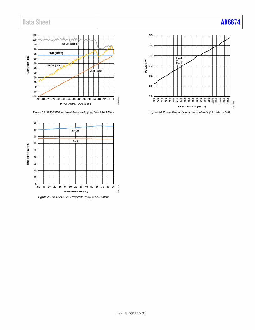
Figure 22. SNR/SFDR vs. Input Amplitude (AIN), fIN = 170.3 MHz
SNR
/SFD
R (d
BFS
)
TEMPERATURE (°C)
0
10
90
80
70
60
50
40
30
20
–50 –40 –30 –20 –10 0 10 20 30 40 50 60 70 80 90
SFDR
SNR
1240
0-21
0
Figure 23. SNR/SFDR vs. Temperature, fIN = 170.3 MHz
2.9
3.0
3.1
SAMPLE RATE (MSPS)
POW
ER (W
)
3.2
3.3
3.4
3.5
700
720
740
760
780
800
820
840
860
880
900
920
940
960
980
1000
1020
1040
1060
1080
1240
0-52
4
L = 4M = 2F = 1
Figure 24. Power Dissipation vs. Sampel Rate (fS) (Default SPI)
AD6674 Data Sheet
Rev. D | Page 18 of 96
AD6674-750 AVDD1 = 1.25 V, AVDD1_SR = 1.25 V, AVDD2 = 2.5 V, AVDD3 = 3.3 V, DVDD = 1.25 V, DRVDD = 1.25 V, SPIVDD = 1.8 V, AIN = −1.0 dBFS, VDR mode (no violation of VDR mask), clock divider = 2, otherwise default SPI settings, TA = 25°C, 128k FFT sample, unless otherwise noted. See Table 10 for recommended settings.
AMPL
ITUD
E (d
BFS)
FREQUENCY (MHz)
–140
–120
–100
–80
–60
–40
–20
0
0 37530022515075 35027520012550 32525017510025
AIN = −1dBFSSNR = 67.3dBFSENOB = 10.7 BITSSFDR = 85dBFSBUFFER CONTROL 1 = 1.5×
1240
0-21
9
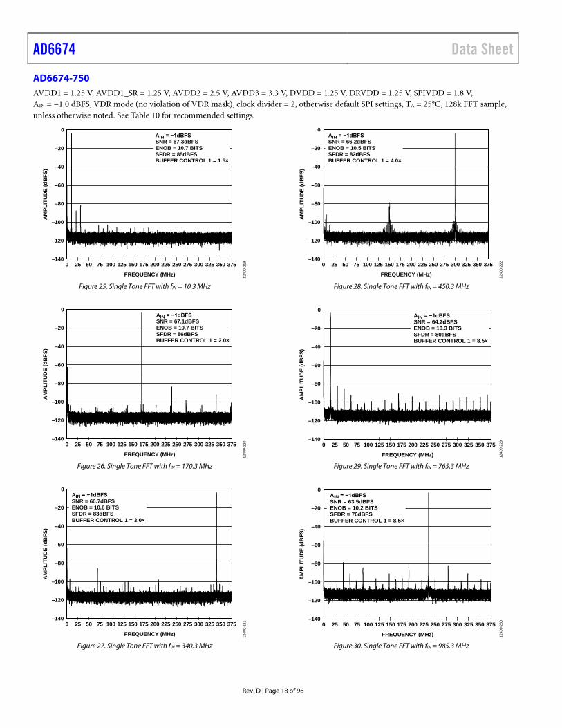
Figure 25. Single Tone FFT with fIN = 10.3 MHz
AMPL
ITUD
E (d
BFS)
FREQUENCY (MHz)
–140
–120
–100
–80
–60
–40
–20
0
0 37530022515075 35027520012550 32525017510025
AIN = −1dBFSSNR = 67.1dBFSENOB = 10.7 BITSSFDR = 86dBFSBUFFER CONTROL 1 = 2.0×
1240
0-22
0
Figure 26. Single Tone FFT with fIN = 170.3 MHz
AMPL
ITUD
E (d
BFS)
FREQUENCY (MHz)
–140
–120
–100
–80
–60
–40
–20
0
0 37530022515075 35027520012550 32525017510025
AIN = −1dBFSSNR = 66.7dBFSENOB = 10.6 BITSSFDR = 83dBFSBUFFER CONTROL 1 = 3.0×
1240
0-22
1
Figure 27. Single Tone FFT with fIN = 340.3 MHz
AMPL
ITUD
E (d
BFS)
FREQUENCY (MHz)
–140
–120
–100
–80
–60
–40
–20
0
0 37530022515075 35027520012550 32525017510025
AIN = −1dBFSSNR = 66.2dBFSENOB = 10.5 BITSSFDR = 82dBFSBUFFER CONTROL 1 = 4.0×
1240
0-22
2
Figure 28. Single Tone FFT with fIN = 450.3 MHz
AM
PLIT
UDE
(dBF
S)
FREQUENCY (MHz)
–140
–120
–100
–80
–60
–40
–20
0
0 37530022515075 35027520012550 32525017510025
AIN = −1dBFSSNR = 64.2dBFSENOB = 10.3 BITSSFDR = 80dBFSBUFFER CONTROL 1 = 8.5×
124
00-2
29
Figure 29. Single Tone FFT with fIN = 765.3 MHz
AMPL
ITUD
E (d
BFS)
FREQUENCY (MHz)
–140
–120
–100
–80
–60
–40
–20
0
0 37530022515075 35027520012550 32525017510025
AIN = −1dBFSSNR = 63.5dBFSENOB = 10.2 BITSSFDR = 76dBFSBUFFER CONTROL 1 = 8.5×
124
00-2
30
Figure 30. Single Tone FFT with fIN = 985.3 MHz
Data Sheet AD6674
Rev. D | Page 19 of 96
AMPL
ITUD
E (d
BFS)
FREQUENCY (MHz)
–140
–120
–100
–80
–60
–40
–20
0
0 37530022515075 35027520012550 32525017510025
AIN = −1dBFSSNR = 62.3dBFSENOB = 9.8 BITSSFDR = 68dBFSBUFFER CONTROL 1 = 8.5×
124
00-2
31
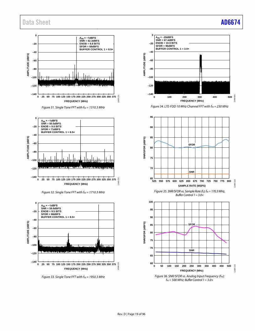
Figure 31. Single Tone FFT with fIN = 1310.3 MHz
AMPL
ITUD
E (d
BFS)
FREQUENCY (MHz)
–140
–120
–100
–80
–60
–40
–20
0
0 37530022515075 35027520012550 32525017510025
AIN = −1dBFSSNR = 60.5dBFSENOB = 9.6 BITSSFDR = 71dBFSBUFFER CONTROL 1 = 8.5×
124
00-2
32
Figure 32. Single Tone FFT with fIN = 1710.3 MHz
AMPL
ITUD
E (d
BFS)
FREQUENCY (MHz)
–140
–120
–100
–80
–60
–40
–20
0
0 37530022515075 35027520012550 32525017510025
AIN = −1dBFSSNR = 59.8dBFSENOB = 9.5 BITSSFDR = 68dBFSBUFFER CONTROL 1 = 8.5×
124
00-2
33
Figure 33. Single Tone FFT with fIN = 1950.3 MHz
0 500400300200100
AMPL
ITUD
E (d
BFS)
FREQUENCY (MHz)
AIN = –20dBFSSNR = 67.4dBFSENOB = 10.9 BITSSFDR = 96dBFSBUFFER CONTROL 1 = 3.0×
1240
0-60
1–140
–120
–100
–80
–60
–40
–20
0
Figure 34. LTE-FDD 10 MHz Channel FFT with fIN = 230 MHz
SNR
/SFD
R (d
BFS
)
SAMPLE RATE (MSPS)
65
70
75
80
85
90
95
525 800775750725700675650625600575550
1240
0-22
3
SNR
SFDR
Figure 35. SNR/SFDR vs. Sample Rate (fS); fIN = 170.3 MHz,
Buffer Control 1 = 3.0×
SNR
/SFD
R (d
BFS
)
FREQUENCY (MHz)
60
65
70
75
80
85
90
100
95
0 50 100 150 200 250 300 350 400 450 500
1240
0-22
5
SFDR
SNR
Figure 36. SNR/SFDR vs. Analog Input Frequency (fIN);
fIN < 500 MHz; Buffer Control 1 = 3.0×
AD6674 Data Sheet
Rev. D | Page 20 of 96
AMPL
ITUD
E (d
BFS)
FREQUENCY (MHz)
–140
–120
–100
–80
–60
–40
–20
0
0 37530022515075 35027520012550 32525017510025
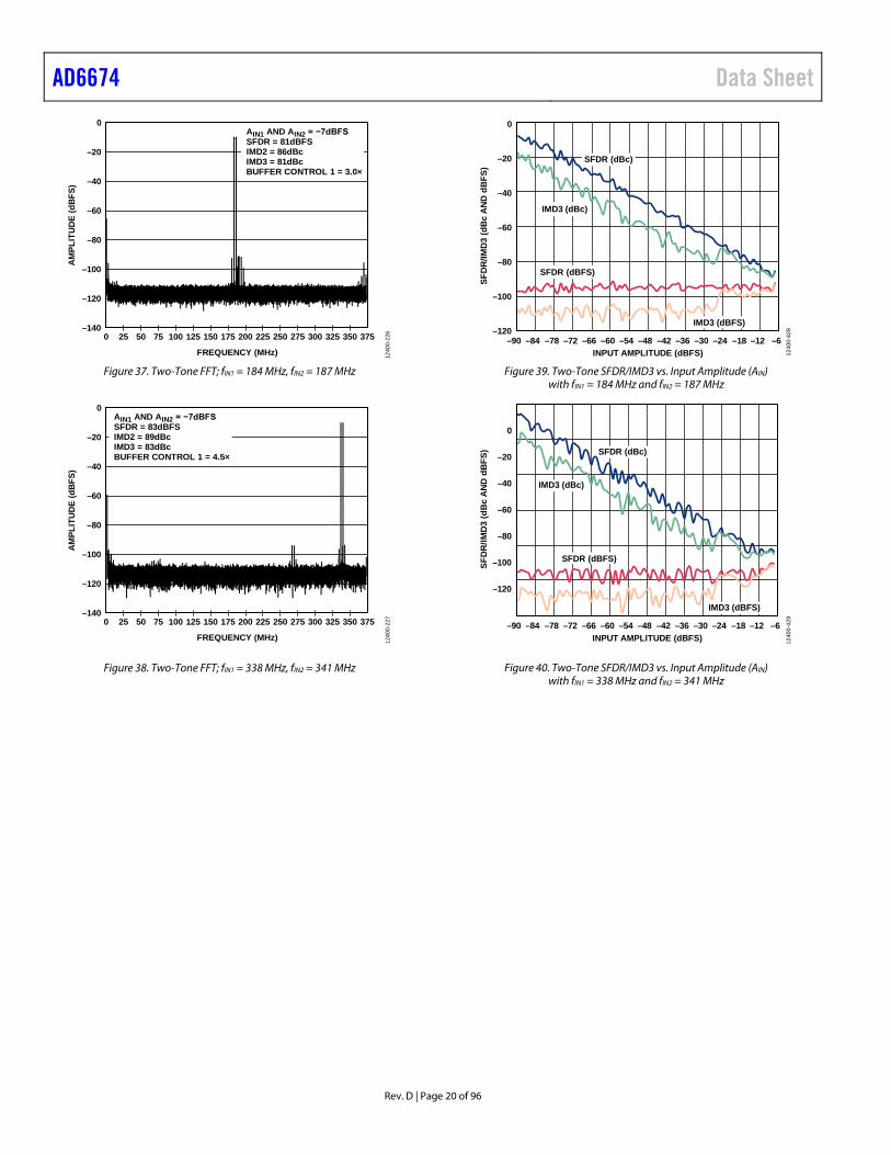
AIN1 AND AIN2 = −7dBFSSFDR = 81dBFSIMD2 = 86dBcIMD3 = 81dBcBUFFER CONTROL 1 = 3.0×
1240
0-22
6
Figure 37. Two-Tone FFT; fIN1 = 184 MHz, fIN2 = 187 MHz
AMPL
ITUD
E (d
BFS)
FREQUENCY (MHz)
–140
–120
–100
–80
–60
–40
–20
0
0 37530022515075 35027520012550 32525017510025
AIN1 AND AIN2 = −7dBFSSFDR = 83dBFSIMD2 = 89dBcIMD3 = 83dBcBUFFER CONTROL 1 = 4.5×
1240
0-22
7
Figure 38. Two-Tone FFT; fIN1 = 338 MHz, fIN2 = 341 MHz
SFD
R/IM
D3
(dB
cA
ND
dB
FS)
INPUT AMPLITUDE (dBFS) 1240
0-42
8–120
–100
–80
–60
–40
–20
0
–90 –84 –78 –72 –66 –60 –54 –48 –42 –36 –30 –24 –18 –12 –6
SFDR (dBFS)
IMD3 (dBFS)
SFDR (dBc)
IMD3 (dBc)
Figure 39. Two-Tone SFDR/IMD3 vs. Input Amplitude (AIN)
with fIN1 = 184 MHz and fIN2 = 187 MHz
SFD
R/IM
D3
(dB
cA
ND
dB
FS)
1240
0-42
9
–120
–100
–80
–60
–40
–20
0
SFDR (dBc)
IMD3 (dBc)
SFDR (dBFS)
IMD3 (dBFS)
INPUT AMPLITUDE (dBFS)–90 –84 –78 –72 –66 –60 –54 –48 –42 –36 –30 –24 –18 –12 –6
Figure 40. Two-Tone SFDR/IMD3 vs. Input Amplitude (AIN) with fIN1 = 338 MHz and fIN2 = 341 MHz
Data Sheet AD6674
Rev. D | Page 21 of 96
0
20
40
60
80
100
120
SNR
/SFD
R (d
Bc
AN
D d
BFS
)
INPUT AMPLITUDE (dBFS) 1240
0-43
0
–90
–85
–80
–75
–70
–65
–60
–55
–50
–45
–40
–35
–30
–25
–20
–15
–10 –5 0
SNR (dBFS)
SFDR (dBFS)
SNR (dBc)
SFDR (dBc)
Figure 41. SNR/SFDR vs. Input Amplitude (AIN), fIN = 170.3 MHz
SNR/
SFDR
(dBF
S)
TEMPERATURE (°C)
65
70
75
80
85
90
95
–40 85603510–15
1240
0-22
8
SNR
SFDR
Figure 42. SNR/SFDR vs. Temperature, fIN = 170.3 MHz
2.3
2.4
2.5
2.6
2.7
POW
ER (W
)
2.8
2.9
3.0
500 550 600 650SAMPLE RATE (MSPS)
700 750 800 850
124
00-2
34
Figure 43. Power Dissipation vs. Sample Rate (fS); L = 4, M = 2, F = 1 for fS ≥ 625 MSPS and L= 2, M = 2, F = 2 for fS < 625 MSPS (Default SPI)
AD6674 Data Sheet
Rev. D | Page 22 of 96
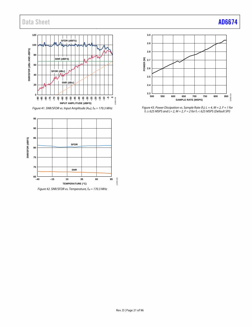
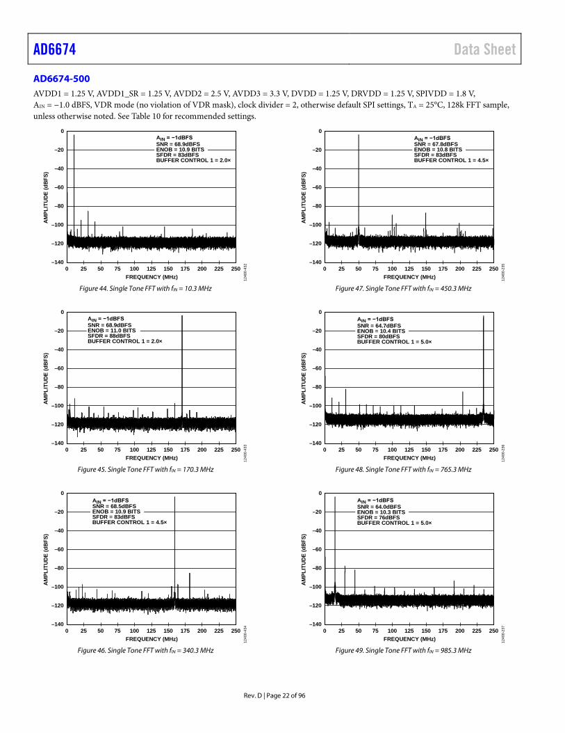
AD6674-500 AVDD1 = 1.25 V, AVDD1_SR = 1.25 V, AVDD2 = 2.5 V, AVDD3 = 3.3 V, DVDD = 1.25 V, DRVDD = 1.25 V, SPIVDD = 1.8 V, AIN = −1.0 dBFS, VDR mode (no violation of VDR mask), clock divider = 2, otherwise default SPI settings, TA = 25°C, 128k FFT sample, unless otherwise noted. See Table 10 for recommended settings.
0 25 50 75 100 125 150 175 200 225 250–140
–120
–100
–80
–60
–40
–20
0
AMPL
ITUD
E (d
BFS)
FREQUENCY (MHz)
AIN = −1dBFSSNR = 68.9dBFSENOB = 10.9 BITSSFDR = 83dBFSBUFFER CONTROL 1 = 2.0×
1240
0-43
2
Figure 44. Single Tone FFT with fIN = 10.3 MHz
0 25 50 75 100 125 150 175 200 225 250–140
–120
–100
–80
–60
–40
–20
0
AMPL
ITUD
E (d
BFS)
FREQUENCY (MHz)
AIN = −1dBFSSNR = 68.9dBFSENOB = 11.0 BITSSFDR = 88dBFSBUFFER CONTROL 1 = 2.0×
1240
0-43
3
Figure 45. Single Tone FFT with fIN = 170.3 MHz
0 25 50 75 100 125 150 175 200 225 250–140
–120
–100
–80
–60
–40
–20
0
AMPL
ITUD
E (d
BFS)
FREQUENCY (MHz)
AIN = −1dBFSSNR = 68.5dBFSENOB = 10.9 BITSSFDR = 83dBFSBUFFER CONTROL 1 = 4.5×
1240
0-43
4
Figure 46. Single Tone FFT with fIN = 340.3 MHz
–140
–120
–100
–80
–60
–40
–20
0
0 25 50 75 100 125 150 175 200 225 250
AMPL
ITUD
E (d
BFS)
FREQUENCY (MHz)
AIN = −1dBFSSNR = 67.8dBFSENOB = 10.8 BITSSFDR = 83dBFSBUFFER CONTROL 1 = 4.5×
1240
0-23
5
Figure 47. Single Tone FFT with fIN = 450.3 MHz
–140
–120
–100
–80
–60
–40
–20
0
0 25 50 75 100 125 150 175 200 225 250
AMPL
ITUD
E (d
BFS)
FREQUENCY (MHz)
AIN = −1dBFSSNR = 64.7dBFSENOB = 10.4 BITSSFDR = 80dBFSBUFFER CONTROL 1 = 5.0×
1240
0-23
6
Figure 48. Single Tone FFT with fIN = 765.3 MHz
–140
–120
–100
–80
–60
–40
–20
0
0 25 50 75 100 125 150 175 200 225 250
AMPL
ITUD
E (d
BFS)
FREQUENCY (MHz)
AIN = −1dBFSSNR = 64.0dBFSENOB = 10.3 BITSSFDR = 76dBFSBUFFER CONTROL 1 = 5.0×
1240
0-23
7
Figure 49. Single Tone FFT with fIN = 985.3 MHz
Data Sheet AD6674
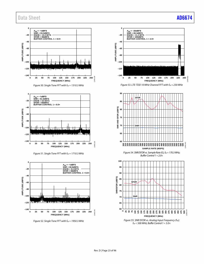
Rev. D | Page 23 of 96
–140
–120
–100
–80
–60
–40
–20
0
0 25 50 75 100 125 150 175 200 225 250
AMPL
ITUD
E (d
BFS)
FREQUENCY (MHz) 1240
0-23
8
AIN = −1dBFSSNR = 63.0dBFSENOB = 10.0 BITSSFDR = 69dBFSBUFFER CONTROL 1 = 8.0×
Figure 50. Single Tone FFT with fIN = 1310.3 MHz
–140
–120
–100
–80
–60
–40
–20
0
0 25 50 75 100 125 150 175 200 225 250
AM
PLIT
UD
E (d
BFS
)
FREQUENCY (MHz)
AIN = −1dBFSSNR = 61.5dBFSENOB = 9.8 BITSSFDR = 69dBFSBUFFER CONTROL 1 = 8.0×
1240
0-23
9
Figure 51. Single Tone FFT with fIN = 1710.3 MHz
–140
–120
–100
–80
–60
–40
–20
0
0 25 50 75 100 125 150 175 200 225 250
AM
PLIT
UD
E (d
BFS
)
FREQUENCY (MHz)
AIN = −1dBFSSNR = 60.8dBFSENOB = 9.6 BITSSFDR = 68dBFSBUFFER CONTROL 1 = 8.0×
1240
0-24
0
Figure 52. Single Tone FFT with fIN = 1950.3 MHz
–140
–120
–100
–80
–60
–40
–20
0
0 25 50 75 100 125 150 175 200 225 250
AMPL
ITUD
E (d
BFS)
FREQUENCY (MHz) 1240
0-60
2
AIN = −20dBFSSNR = 69.3dBFSENOB = 11.2 BITSSFDR = 100dBFSBUFFER CONTROL 1 = 2.0×
Figure 53. LTE-TDD 10 MHz Channel FFT with fIN = 230 MHz
60
65
70
75
80
85
90
300
310
320
330
340
350
360
370
380
390
400
410
SNR
AN
D S
FDR
(dB
FS)
SAMPLE RATE (MSPS)42
043
044
045
046
047
048
049
050
052
053
054
055
056
057
058
059
0
SNR
SFDR
1240
0-44
2
Figure 54. SNR/SFDR vs. Sample Rate (fS), fIN = 170.3 MHz;
Buffer Control 1 = 2.0×
60
65
70
75
80
85
90
95
100
0 25 50 75 100
125
150
175
200
225
250
275
300
325
350
375
400
425
450
475
500
SNR/
SFDR
(dBF
S)
FREQUENCY (MHz)
SNR
SFDR
1240
0-44
4
Figure 55. SNR/SFDR vs. Analog Input Frequency (fIN);
fIN < 500 MHz; Buffer Control 1 = 3.0×
AD6674 Data Sheet
Rev. D | Page 24 of 96
–120
–100
–80
–60
–40
–20
0
AMPL
ITUD
E (d
BFS)
0 50 100 150 200 250FREQUENCY (MHz)
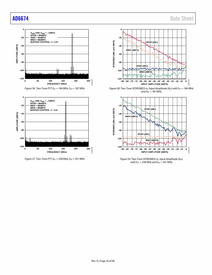
AIN1 AND AIN2 = –7dBFSSFDR = 88dBFSIMD2 = 94dBFSIMD3 = 88dBFSBUFFER CONTROL 1 = 2.0×
1240
0-44
5
Figure 56. Two-Tone FFT; fIN1 = 184 MHz, fIN2 = 187 MHz
–120
–100
–80
–60
–40
–20
0
0 50 100 150 200 250
AMPL
ITUD
E (d
BFS)
FREQUENCY (MHz)
AIN1 AND AIN2 = –7dBFSSFDR = 88dBFSIMD2 = 88dBFSIMD3 = 89dBFSBUFFER CONTROL 1 = 4.5×
1240
0-44
6
Figure 57. Two-Tone FFT; fIN1 = 338 MHz, fIN2 = 341 MHz
INPUT AMPLITUDE (dBFS)–90 –84 –78 –72 –66 –60 –54 –48 –42 –36 –30 –24 –18 –12 –6
–120
–100
–80
–60
–40
0
–20
SFDR
/IMD3
(dBc
and
dBF
S) SFDR (dBc)
SFDR (dBc)
IMD3 (dBFS)
IMD3 (dBFS)
1240
0-44
7
Figure 58. Two-Tone SFDR/IMD3 vs. Input Amplitude (AIN) with fIN1 = 184 MHz
and fIN2 = 187 MHz
INPUT AMPLITUDE (dBFS)–90 –84 –78 –72 –66 –60 –54 –48 –42 –36 –30 –24 –18 –12 –6
–120
–100
–80
–60
–40
0
–20
SFDR
/IMD3
(dBc
and
dBF
S) SFDR (dBc)
SFDR (dBc)
IMD3 (dBFS)
IMD3 (dBFS)
1240
0-44
8
Figure 59. Two-Tone SFDR/IMD3 vs. Input Amplitude (AIN) with fIN1 = 338 MHz and fIN2 = 341 MHz
Data Sheet AD6674
Rev. D | Page 25 of 96
–20
–10
0
10
20
30
40
50
60
70
80
90
100
110–9
0–8
5–8
0–7
5–7
0–6
5–6
0–5
5–5
0–4
5–4
0–3
5–3
0–2
5–2
0–1
5–1
0 –5 0
SNR
/SFD
R (d
Bc
and
dBFS
)
INPUT AMPLITUDE (dBFS)
SFDR (dBFS)
SNR (dBFS)
SFDR (dBc)
SNR (dBc)
1240
0-44
9
Figure 60. SNR/SFDR vs. Input Amplitude (AIN), fIN = 170.3 MHz
65
70
75
80
85
90
95
–40 –15 10 35 60 85
SNR/
SFDR
(dBF
S)
TEMPERATURE (°C) 1240
0-45
0
SFDR
SNR
Figure 61. SNR/SFDR vs. Temperature, fIN = 170.3 MHz
1.90
1.95
2.00
2.05
2.10
2.15
2.20
2.25
2.30
2.35
2.40
300
320
340
360
380
400
420
440
460
480
500
520
540
560
580
POW
ER (W
)
SAMPLE RATE (MSPS) 1240
0-45
1
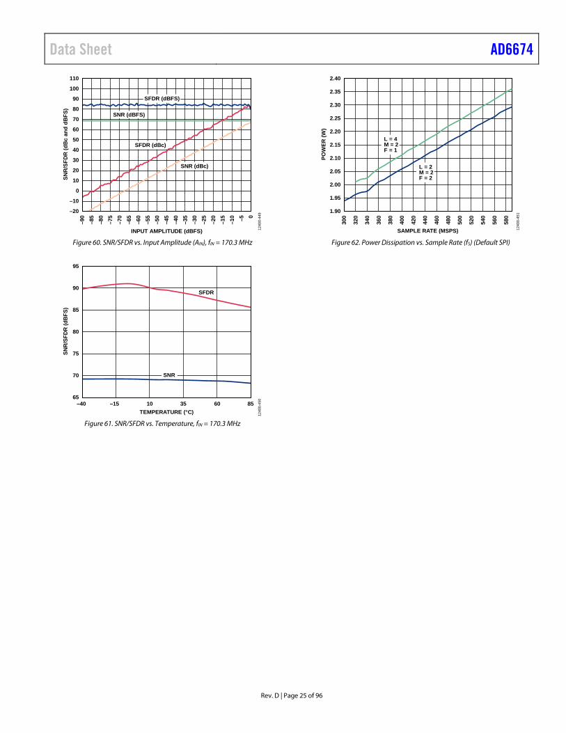
L = 4M = 2F = 1
L = 2M = 2F = 2
Figure 62. Power Dissipation vs. Sample Rate (fS) (Default SPI)
AD6674 Data Sheet
Rev. D | Page 26 of 96
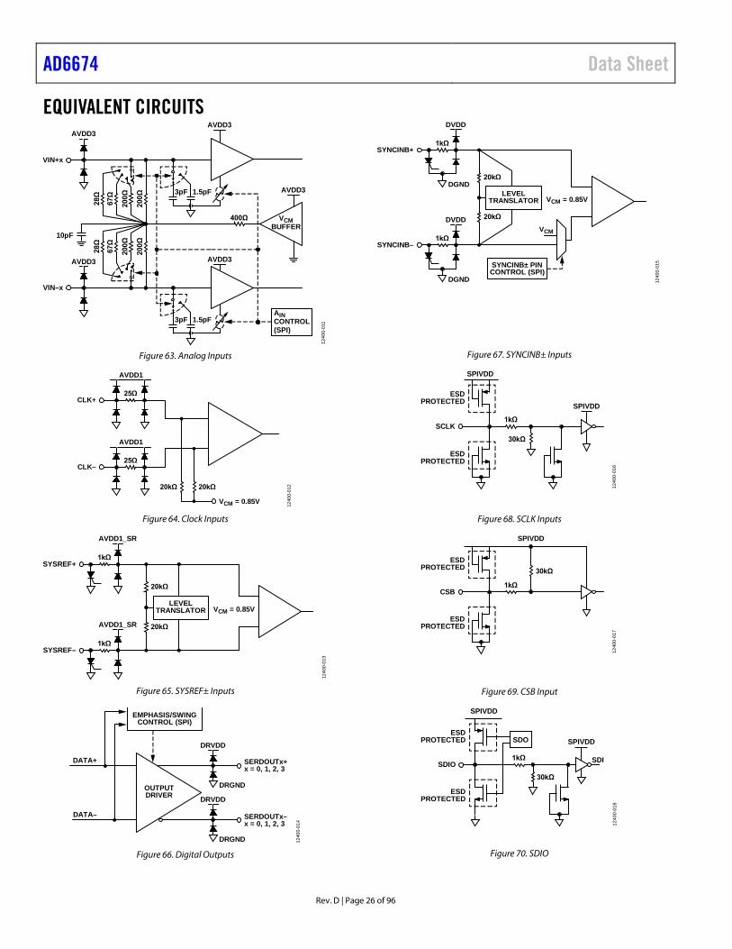
EQUIVALENT CIRCUITS
AINCONTROL(SPI)
10pF
VIN+x
VIN–x
AVDD3
AVDD3
AVDD3
VCMBUFFER
400Ω
200Ω
200Ω
67Ω
28Ω
200Ω
200Ω
67Ω
28Ω
AVDD3
AVDD3
1.5pF3pF
1.5pF3pF12
400-
011
Figure 63. Analog Inputs
CLK+
CLK–
AVDD1
25Ω
AVDD1
25Ω
20kΩ20kΩ
VCM = 0.85V 1240
0-01
2
Figure 64. Clock Inputs
SYSREF+
AVDD1_SR
1kΩ
SYSREF–
AVDD1_SR
1kΩ
20kΩ
20kΩ
LEVELTRANSLATOR VCM = 0.85V
1240
0-01
3
Figure 65. SYSREF± Inputs
DRVDD
DRGND
DRVDD
DRGND
OUTPUTDRIVER
EMPHASIS/SWINGCONTROL (SPI)
DATA+
DATA–
SERDOUTx+x = 0, 1, 2, 3
SERDOUTx–x = 0, 1, 2, 3
1240
0-01
4
Figure 66. Digital Outputs
20kΩ
20kΩ
LEVELTRANSLATOR VCM = 0.85V
SYNCINB± PINCONTROL (SPI)
SYNCINB+
DVDD
1kΩ
DGND
SYNCINB–
DVDD
1kΩ
DGND
VCM
1240
0-01
5
Figure 67. SYNCINB± Inputs
30kΩ
SPIVDDESD
PROTECTED
ESDPROTECTED
1kΩ
SPIVDD
SCLK
1240
0-01
6
Figure 68. SCLK Inputs
30kΩESD
PROTECTED
ESDPROTECTED
1kΩ
SPIVDD
CSB
1240
0-01
7
Figure 69. CSB Input
30kΩ
ESDPROTECTED
ESDPROTECTED
1kΩ
SPIVDD
SPIVDD
SDISDIO
SDO
1240
0-01
8
Figure 70. SDIO
Data Sheet AD6674
Rev. D | Page 27 of 96
ESDPROTECTED
ESDPROTECTED
SPIVDD
FD_A/FD_B
FD
JESD LMFC
FD_x PIN CONTROL (SPI)
JESD SYNC~
TEMPERATURE DIODE(FD_A ONLY)
1240
0-01
9
Figure 71. FD_A/FD_B Outputs
ESDPROTECTED
ESDPROTECTED
1kΩ
SPIVDD
PDWN/STBY
PDWNCONTROL (SPI)
1240
0-02
0
Figure 72. PDWN/STBY Input
ESDPROTECTED
ESDPROTECTED
V_1P0
V_1P0 PINCONTROL (SPI)
AVDD2
1240
0-02
1
Figure 73. V_1P0 Input/Output
AD6674 Data Sheet
Rev. D | Page 28 of 96
THEORY OF OPERATION The AD6674 has two analog input channels and two JESD204B output lane pairs. The AD6674 is designed to sample wide bandwidth analog signals of up to 2 GHz. The AD6674 is optimized for wide input bandwidth, high sampling rate, excellent linearity, and low power in a small package.
The dual ADC cores feature a multistage, differential pipelined architecture with integrated output error correction logic. Each ADC features wide bandwidth inputs supporting a variety of user-selectable input ranges. An integrated voltage reference eases design considerations.
The AD6674 has several functions that simplify the AGC function in a communications receiver. The programmable threshold detector allows monitoring of the incoming signal power using the fast detect bits of the ADC output data stream, which are enabled and programmed via Register 0x245 through Register 0x24C. If the input signal level exceeds the programmable threshold, the fast detect indicator goes high. Because this threshold indicator has low latency, the user can quickly lower the system gain to avoid an overrange condition at the ADC input.
The Subclass 1 JESD204B-based high speed serialized output data rate can be configured in one-lane (L = 1) and two-lane (L = 2) configurations depending upon the sample rate and the decimation ratio. Multidevice synchronization is supported through the SYSREF± and SYNCINB± input pins.
ADC ARCHITECTURE The architecture consists of an input buffered pipelined ADC. The input buffer is designed to provide a termination imped-ance to the analog input signal. This termination impedance can be changed using the SPI to meet the termination needs of the driver/amplifier. The default termination value is set to 400 Ω. The equivalent circuit diagram of the analog input termination is shown in Figure 63. The input buffer is optimized for high linearity, low noise, and low power.
The input buffer provides a linear high input impedance (for ease of drive) and reduces the kickback from the ADC. The quantized outputs from each stage are combined into a final 16-bit result in the digital correction logic. The pipelined architecture permits the first stage to operate with a new input sample while the remaining stages operate with preceding samples. Sampling occurs on the rising edge of the clock.
ANALOG INPUT CONSIDERATIONS The analog input to the AD6674 is a differential buffer. The internal common-mode voltage of the buffer is 2.05 V. The clock signal alternately switches the input circuit between sample mode and hold mode. When the input circuit is switched into sample mode, the signal source must be capable of charging the sample capacitors and settling within one-half of a clock cycle. A small resistor, in series with each input, can help reduce the peak transient current inserted from the output stage of the
driving source. In addition, low Q inductors or ferrite beads can be placed on each section of the input to reduce high differen-tial capacitance at the analog inputs and, thus, achieve the maximum bandwidth of the ADC. Such use of low Q inductors or ferrite beads is required when driving the converter front end at high IF frequencies. Place either a differential capacitor or two single-ended capacitors on the inputs to provide a matching passive network. This ultimately creates a low-pass filter at the input, which limits unwanted broadband noise. For more infor-mation, refer to the AN-742 Application Note, the AN-827 Application Note, and the Analog Dialogue article “Transformer-Coupled Front-End for Wideband A/D Converters” (Volume 39, April 2005) at www.analog.com. In general, the precise values depend on the application.
For best dynamic performance, match the source impedances driving VIN+x and VIN−x such that common-mode settling errors are symmetrical. These errors are reduced by the common-mode rejection of the ADC. An internal reference buffer creates a differential reference that defines the span of the ADC core.
Maximum SNR performance is achieved by setting the ADC to the largest span in a differential configuration. In the case of the AD6674, the available span is programmable through the SPI port from 1.46 V p-p to 2.06 V p-p differential, with 1.70 V p-p differential being the default for the AD6674-1000 and AD6674-750, whereas the default for the AD6674-500 is 2.06 V p-p.
Differential Input Configurations
There are several ways to drive the AD6674, either actively or passively. However, optimum performance is achieved by driving the analog input differentially.
For applications where SNR and SFDR are key parameters, differential transformer coupling is the recommended input configuration (see Figure 74 and Table 9) because the noise performance of most amplifiers is not adequate to achieve the true performance of the AD6674.
For low to midrange frequencies, it is recommended to use a double balun or double transformer network (see Figure 74) for optimum performance from the AD6674. For higher frequencies in the second or third Nyquist zone, it is better to remove some of the front-end passive components to ensure wideband operation (see Figure 74 and Table 9).
ADC
R1
R2
R1 0.1µF
0.1µF
0.1µFC2
R3
R3
BALUN
NOTES1. SEE TABLE 9 FOR COMPONENT VALUES.
R2
C1
C1
1240
0-51
6
Figure 74. Differential Transformer Coupled Configuration for AD6674
Data Sheet AD6674
Rev. D | Page 29 of 96
Table 9. Differential Transformer Coupled Input Configuration Component Values Device Frequency Range Transformer R1 (Ω) R2 (Ω) R3 (Ω) C1 (pF) C2 (pF) AD6674-500 DC to 250 MHz ETC1-1-13 10 50 10 4 2 250 MHz to 2 GHz BAL0006/BAL0006SMG 10 50 10 4 2 AD6674-750 DC to 375 MHz ETC1-1-13 10 50 10 4 2 375 MHz to 2 GHz BAL0006/BAL0006SMG 10 50 10 4 2 AD6674-1000 DC to 500 MHz ECT1-1-13/BAL0006SMG 25 25 10 4 2 500 MHz to 2 GHz BAL0006/BAL0006SMG 25 25 0 Open Open
Input Common Mode
The analog inputs of the AD6674 are internally biased to the common mode, as shown in Figure 75. The common-mode buffer has limited range in that the performance suffers greatly if the common-mode voltage drops by more than 100 mV. Therefore, in dc-coupled applications, set the common-mode voltage to 2.05 V ± 100 mV to ensure proper ADC operation.
Analog Input Controls and SFDR Optimization
The AD6674 offers flexible controls for the analog inputs such as input termination, input capacitance, buffer current, and input full-scale adjustment. All of the available controls are shown in Figure 75.
10pF
VIN+x
VIN–x
AVDD3
AVDD3
AVDD3
VCMBUFFER
400Ω
200Ω
200Ω
67Ω
28Ω
200Ω
200Ω
67Ω
28Ω
AVDD3
AVDD3
1.5pF3pF
1.5pF3pF
AIN CONTROLSPI REGISTERS(0x008, 0x015,0x016, 0x018,0x019, 0x01A,0x11A, 0x934,
0x935)
1240
0-51
7
Figure 75. Analog Input Controls
Use Register 0x018, Register 0x019, Register 0x01A, Register 0x11A, Register 0x934, and Register 0x935 to adjust the buffer behavior on each channel to optimize the SFDR over various input frequencies and bandwidths of interest.
Input Buffer Control Registers (Register 0x018, Register 0x019, Register 0x01A, Register 0x934, Register 0x935, Register 0x11A)
The input buffer has many registers that set the bias currents and other settings for operation at different frequencies. These bias currents and settings can be changed to suit the input frequency range of operation. Register 0x018 controls the buffer bias current to reduce the effects of charge kickback from the ADC core. This setting can be scaled from a low setting of 1.0× to
a high setting of 8.5×. The default setting in Register 0x018 is 3.0× for the AD6674-750 and AD6674-1000, whereas the default for the AD6674-500 is 2.0×. These settings are sufficient for operation in the first Nyquist zone. As the input buffer currents are set, the amount of current required by the AVDD3 supply changes. This relationship is shown in Figure 76. For a complete list of buffer current settings, see Table 45 for more details.
1240
0-34
150
100
150
200
250
300
150 250 350 450 550 650 750 850
I AVD
D3
(mA
)
BUFFER CURRENT SETTING
AD6674-1000AND
AD6674-750
AD6674-500
Figure 76. IAVDD3 vs. Buffer Current Setting in Register 0x018
Register 0x019, Register 0x01A, Register 0x11A, and Register 0x935 offer secondary bias controls for the input buffer for frequencies >500 MHz. Register 0x934 can be used to reduce input capacitance to achieve wider signal bandwidth but doing so may result in slightly lower linearity and noise performance. These register settings do not affect the AVDD3 power as much as Register 0x018 does. For frequencies <500 MHz, it is recommended to use the default settings for these registers. Table 10 shows the recom-mended values for the buffer current control registers for various speed grades.
Use Register 0x11A when sampling in higher Nyquist zones (>500 MHz for the AD6674-1000). This setting enables the ADC sampling network to optimize the sampling and settling times internal to the ADC for high frequency operation. For frequencies greater than 500 MHz, it is recommended to operate the ADC core at a 1.46 V full-scale setting irrespective of the speed grade. This setting offers better SFDR without any significant decrease in SNR.
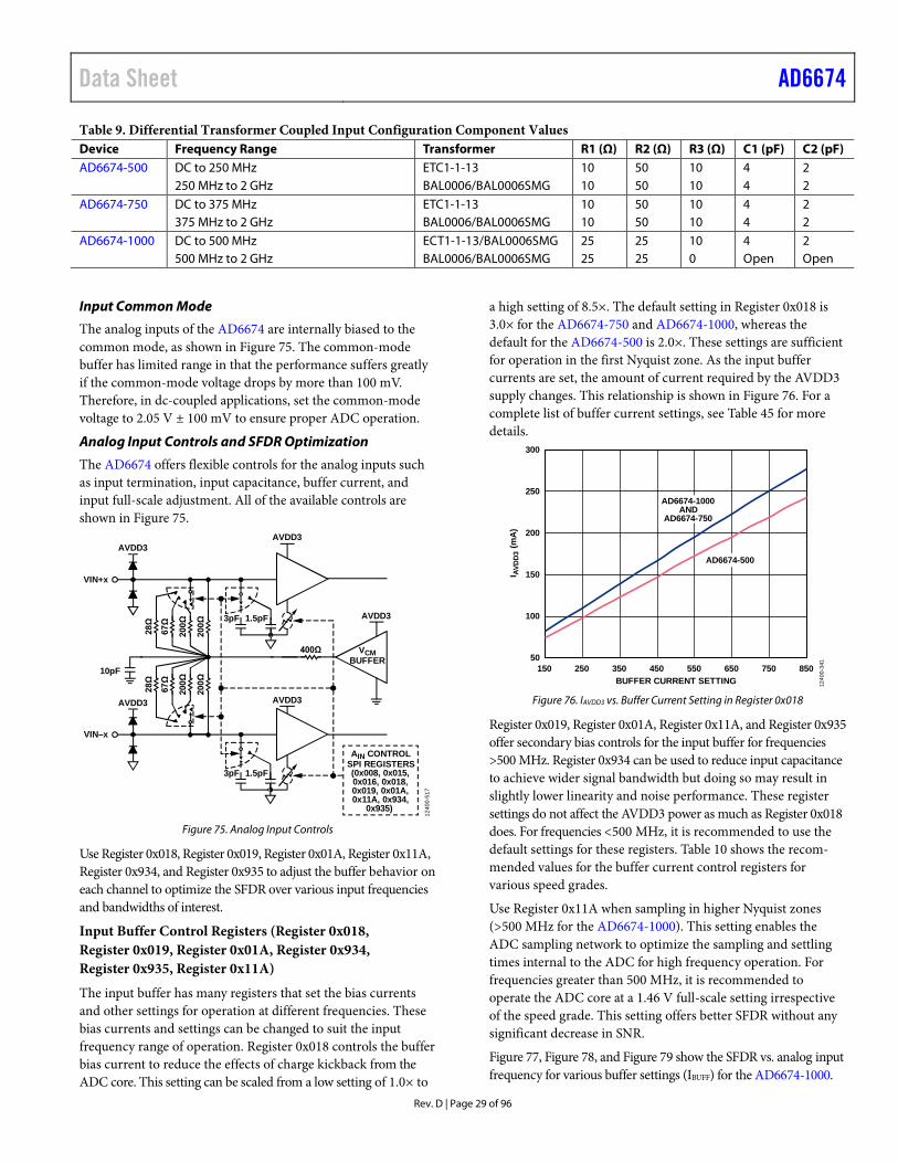
Figure 77, Figure 78, and Figure 79 show the SFDR vs. analog input frequency for various buffer settings (IBUFF) for the AD6674-1000.
AD6674 Data Sheet
Rev. D | Page 30 of 96
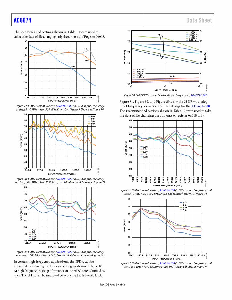
The recommended settings shown in Table 10 were used to collect the data while changing only the contents of Register 0x018.
SFD
R (d
BFS
)
INPUT FREQUENCY (MHz) 1240
0-34
250
55
60
65
70
75
80
85
90
10 60 110 160 210 260 310 360 410 460
1.5×
3.0×
4.5×
Figure 77. Buffer Current Sweeps, AD6674-1000 (SFDR vs. Input Frequency and IBUFF); 10 MHz < fIN < 500 MHz; Front-End Network Shown in Figure 74
40
45
50
55
60
65
70
75
80
85
SFD
R (d
BFS
)
INPUT FREQUENCY (MHz)
503.4 677.6 851.9 1026.2 1200.5 1374.8
3.0×4.0×5.0×6.0×
1240
0-45
2
Figure 78. Buffer Current Sweeps, AD6674-1000 (SFDR vs. Input Frequency
and IBUFF); 500 MHz < fIN < 1500 MHz; Front-End Network Shown in Figure 74
40
45
50
55
60
65
70
75
80
SFD
R (d
BFS
)
INPUT FREQUENCY (MHz)
1513.4 1607.4 1701.5 1795.6 1889.8
4.5×5.5×6.5×7.5×8.5×
1240
0-45
3
Figure 79. Buffer Current Sweeps, AD6674-1000 (SFDR vs. Input Frequency and IBUFF); 1500 MHz < fIN < 2 GHz; Front-End Network Shown in Figure 74
In certain high frequency applications, the SFDR can be improved by reducing the full-scale setting, as shown in Table 10. At high frequencies, the performance of the ADC core is limited by jitter. The SFDR can be improved by reducing the full-scale level.
1.52GHz1.65GHz1.76GHz1.9GHz1.95GHz
55
60
65
70
75
80
55
60
65
70
75
80
–3 –2 –1
SFD
R (d
BFS
)
SNR
(dB
c)
INPUT LEVEL (dBFS) 1240
0-45
4
1.52GHz1.65GHz1.76GHz1.9GHz1.95GHz
Figure 80. SNR/SFDR vs. Input Level and Input Frequencies, AD6674-1000
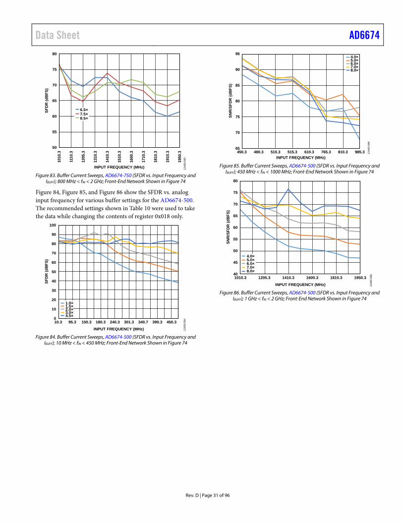
Figure 81, Figure 82, and Figure 83 show the SFDR vs. analog input frequency for various buffer settings for the AD6674-500. The recommended settings shown in Table 10 were used to take the data while changing the contents of register 0x018 only.
55
60
65
70
75
80
85
90
95
10.3
65.3
95.3
125.
3
150.
3
170.
3
180.
3
SFD
R (d
BFS
)
INPUT FREQUENCY (MHz)
210.
3
240.
3
270.
3
301.
3
330.
3
340.
7
360.
3
390.
3
420.
3
450.
3
1.5×2.0×2.5×3.5×4.5×
1240
0-58
1
Figure 81. Buffer Current Sweeps, AD6674-750 (SFDR vs. Input Frequency and
IBUFF); 10 MHz < fIN < 450 MHz; Front-End Network Shown in Figure 74
SFDR
(dBF
S)
INPUT FREQUENCY (MHz) 1240
0-58
260
65
70
75
80
85
90
95
450.3 480.3 510.3 515.3 610.3 765.3 810.3 985.3 1010.3
4.5×5.5×6.5×7.5×
Figure 82. Buffer Current Sweeps, AD6674-750 (SFDR vs. Input Frequency and
IBUFF); 450 MHz < fIN < 800 MHz; Front-End Network Shown in Figure 74
Data Sheet AD6674
Rev. D | Page 31 of 96
50
55
60
65
70
75
8010
10.3
1110
.3
1205
.3
1310
.3
1410
.3
1510
.3
1600
.3
1710
.3
1810
.3
1910
.3
1950
.3
SFDR
(dBF
S)
INPUT FREQUENCY (MHz) 1240
0-58
3
6.5×7.5×8.5×
Figure 83. Buffer Current Sweeps, AD6674-750 (SFDR vs. Input Frequency and
IBUFF); 800 MHz < fIN < 2 GHz; Front-End Network Shown in Figure 74
Figure 84, Figure 85, and Figure 86 show the SFDR vs. analog input frequency for various buffer settings for the AD6674-500. The recommended settings shown in Table 10 were used to take the data while changing the contents of register 0x018 only.
0
10
20
30
40
50
60
70
80
90
100
10.3 95.3 150.3 180.3 240.3 301.3 340.7 390.3 450.3
SFDR
(dBF
S)
INPUT FREQUENCY (MHz)
1.0×1.5×2.0×3.0×4.5×
1240
0-58
4
Figure 84. Buffer Current Sweeps, AD6674-500 (SFDR vs. Input Frequency and
IBUFF); 10 MHz < fIN < 450 MHz; Front-End Network Shown in Figure 74
65
70
75
80
85
90
95
450.3 480.3 510.3 515.3 610.3 765.3 810.3 985.3
SNR
/SFD
R (d
BFS
)
4.0×5.0×6.0×7.0×8.0×
1240
0-58
5
INPUT FREQUENCY (MHz) Figure 85. Buffer Current Sweeps, AD6674-500 (SFDR vs. Input Frequency and
IBUFF); 450 MHz < fIN < 1000 MHz; Front-End Network Shown in Figure 74
SNR/
SFDR
(dBF
S)
40
45
50
55
60
65
70
75
80
1010.3 1205.3 1410.3 1600.3 1810.3 1950.3
INPUT FREQUENCY (MHz)
4.0×5.0×6.0×7.0×8.0×
1240
0-58
6
Figure 86. Buffer Current Sweeps, AD6674-500 (SFDR vs. Input Frequency and
IBUFF); 1 GHz < fIN < 2 GHz; Front-End Network Shown in Figure 74
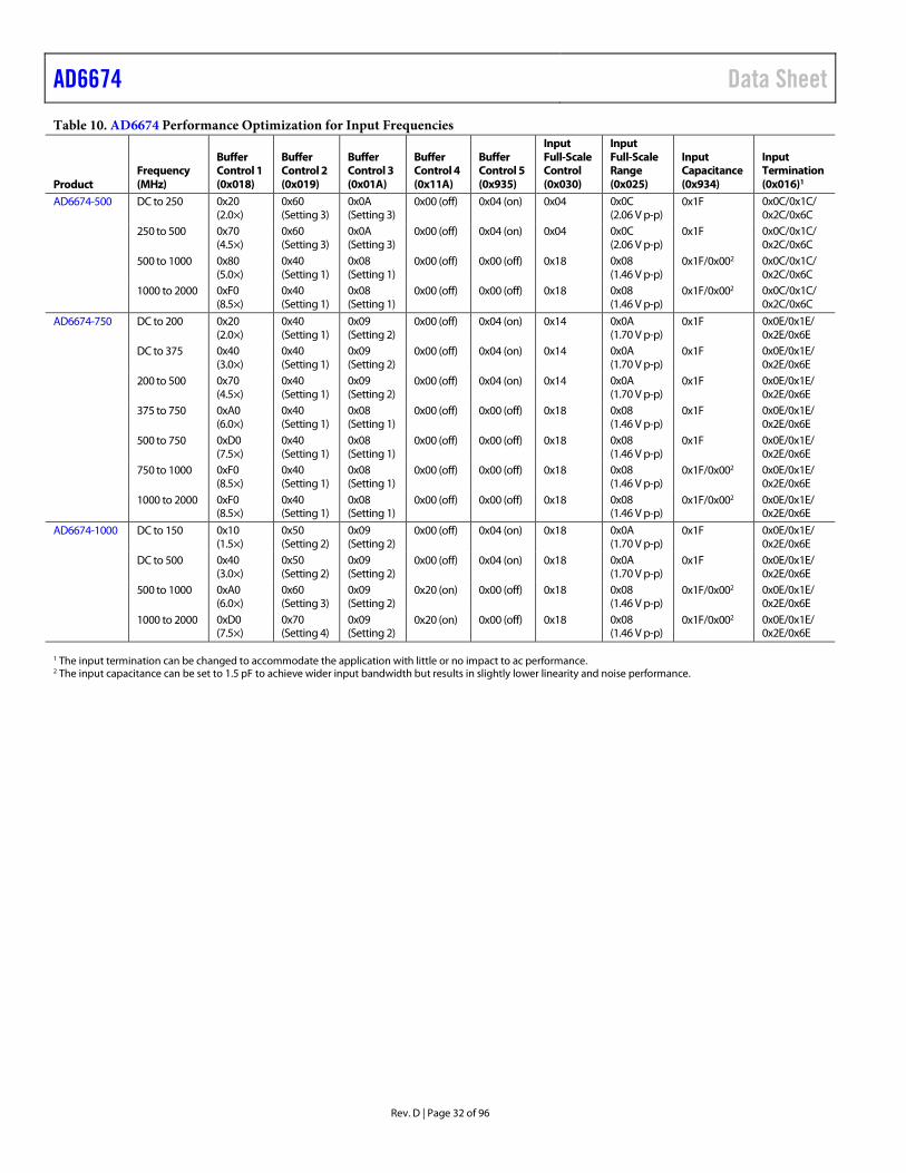
AD6674 Data Sheet
Rev. D | Page 32 of 96
Table 10. AD6674 Performance Optimization for Input Frequencies
Product Frequency (MHz)
Buffer Control 1 (0x018)
Buffer Control 2 (0x019)
Buffer Control 3 (0x01A)
Buffer Control 4 (0x11A)
Buffer Control 5 (0x935)
Input Full-Scale Control (0x030)
Input Full-Scale Range (0x025)
Input Capacitance (0x934)
Input Termination (0x016)1
AD6674-500 DC to 250 0x20 (2.0×)
0x60 (Setting 3)
0x0A (Setting 3)
0x00 (off) 0x04 (on) 0x04 0x0C (2.06 V p-p)
0x1F 0x0C/0x1C/ 0x2C/0x6C
250 to 500 0x70 (4.5×)
0x60 (Setting 3)
0x0A (Setting 3)
0x00 (off) 0x04 (on) 0x04 0x0C (2.06 V p-p)
0x1F 0x0C/0x1C/ 0x2C/0x6C
500 to 1000 0x80 (5.0×)
0x40 (Setting 1)
0x08 (Setting 1)
0x00 (off) 0x00 (off) 0x18 0x08 (1.46 V p-p)
0x1F/0x002 0x0C/0x1C/ 0x2C/0x6C
1000 to 2000 0xF0 (8.5×)
0x40 (Setting 1)
0x08 (Setting 1)
0x00 (off) 0x00 (off) 0x18 0x08 (1.46 V p-p)
0x1F/0x002 0x0C/0x1C/ 0x2C/0x6C
AD6674-750 DC to 200 0x20 (2.0×)
0x40 (Setting 1)
0x09 (Setting 2)
0x00 (off) 0x04 (on) 0x14 0x0A (1.70 V p-p)
0x1F 0x0E/0x1E/ 0x2E/0x6E
DC to 375 0x40 (3.0×)
0x40 (Setting 1)
0x09 (Setting 2)
0x00 (off) 0x04 (on) 0x14 0x0A (1.70 V p-p)
0x1F 0x0E/0x1E/ 0x2E/0x6E
200 to 500 0x70 (4.5×)
0x40 (Setting 1)
0x09 (Setting 2)
0x00 (off) 0x04 (on) 0x14 0x0A (1.70 V p-p)
0x1F 0x0E/0x1E/ 0x2E/0x6E
375 to 750 0xA0 (6.0×)
0x40 (Setting 1)
0x08 (Setting 1)
0x00 (off) 0x00 (off) 0x18 0x08 (1.46 V p-p)
0x1F 0x0E/0x1E/ 0x2E/0x6E
500 to 750 0xD0 (7.5×)
0x40 (Setting 1)
0x08 (Setting 1)
0x00 (off) 0x00 (off) 0x18 0x08 (1.46 V p-p)
0x1F 0x0E/0x1E/ 0x2E/0x6E
750 to 1000 0xF0 (8.5×)
0x40 (Setting 1)
0x08 (Setting 1)
0x00 (off) 0x00 (off) 0x18 0x08 (1.46 V p-p)
0x1F/0x002 0x0E/0x1E/ 0x2E/0x6E
1000 to 2000 0xF0 (8.5×)
0x40 (Setting 1)
0x08 (Setting 1)
0x00 (off) 0x00 (off) 0x18 0x08 (1.46 V p-p)
0x1F/0x002 0x0E/0x1E/ 0x2E/0x6E
AD6674-1000 DC to 150 0x10 (1.5×)
0x50 (Setting 2)
0x09 (Setting 2)
0x00 (off) 0x04 (on) 0x18 0x0A (1.70 V p-p)
0x1F 0x0E/0x1E/ 0x2E/0x6E
DC to 500 0x40 (3.0×)
0x50 (Setting 2)
0x09 (Setting 2)
0x00 (off) 0x04 (on) 0x18 0x0A (1.70 V p-p)
0x1F 0x0E/0x1E/ 0x2E/0x6E
500 to 1000 0xA0 (6.0×)
0x60 (Setting 3)
0x09 (Setting 2)
0x20 (on) 0x00 (off) 0x18 0x08 (1.46 V p-p)
0x1F/0x002 0x0E/0x1E/ 0x2E/0x6E
1000 to 2000 0xD0 (7.5×)
0x70 (Setting 4)
0x09 (Setting 2)
0x20 (on) 0x00 (off) 0x18 0x08 (1.46 V p-p)
0x1F/0x002 0x0E/0x1E/ 0x2E/0x6E
1 The input termination can be changed to accommodate the application with little or no impact to ac performance. 2 The input capacitance can be set to 1.5 pF to achieve wider input bandwidth but results in slightly lower linearity and noise performance.
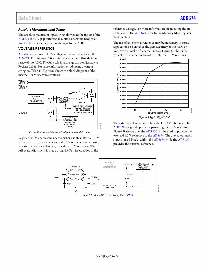
Data Sheet AD6674
Rev. D | Page 33 of 96
Absolute Maximum Input Swing
The absolute maximum input swing allowed at the inputs of the AD6674 is 4.3 V p-p differential. Signals operating near or at this level can cause permanent damage to the ADC.
VOLTAGE REFERENCE A stable and accurate 1.0 V voltage reference is built into the AD6674. This internal 1.0 V reference sets the full-scale input range of the ADC. The full-scale input range can be adjusted via Register 0x025. For more information on adjusting the input swing, see Table 45. Figure 87 shows the block diagram of the internal 1.0 V reference controls.
ADCCOREFULL-SCALE
VOLTAGEADJUST
V_1P0 PINCONTROL SPI
REGISTER(0x025 AND
0x024)
V_1P0
VIN–A/VIN–B
VIN+A/VIN+B
INTERNALV_1P0
GENERATOR
INPUT FULL-SCALERANGE ADJUSTSPI REGISTER
(0x025 AND 0x024)
1240
0-03
1
Figure 87. Internal Reference Configuration and Controls
Register 0x024 enables the user to either use this internal 1.0 V reference or to provide an external 1.0 V reference. When using an external voltage reference, provide a 1.0 V reference. The full-scale adjustment is made using the SPI, irrespective of the
reference voltage. For more information on adjusting the full-scale level of the AD6674, refer to the Memory Map Register Table section.
The use of an external reference may be necessary, in some applications, to enhance the gain accuracy of the ADC or improve thermal drift characteristics. Figure 88 shows the typical drift characteristics of the internal 1.0 V reference.
–50 0 25 90
V_1P
0 VO
LTAG
E (V
)
TEMPERATURE (°C)
0.9998
0.9999
1.0000
1.0001
1.0002
1.0003
1.0004
1.0005
1.0006
1.0007
1.0008
1.0009
1.0010
1240
0-10
6
Figure 88. Typical V_1P0 Drift
The external reference must be a stable 1.0 V reference. The ADR130 is a good option for providing the 1.0 V reference. Figure 89 shows how the ADR130 can be used to provide the external 1.0 V reference to the AD6674. The grayed out areas show unused blocks within the AD6674 while the ADR130 provides the external reference.
FULL-SCALEVOLTAGEADJUST
V_1P0
0.1µF
VOUT 4
SET 5
NC 6
VIN3
GND2
NC1
ADR130
0.1µF
INPUT
FULL-SCALECONTROL
INTERNALV_1P0
GENERATOR
1240
0-03
2
Figure 89. External Reference Using the ADR130
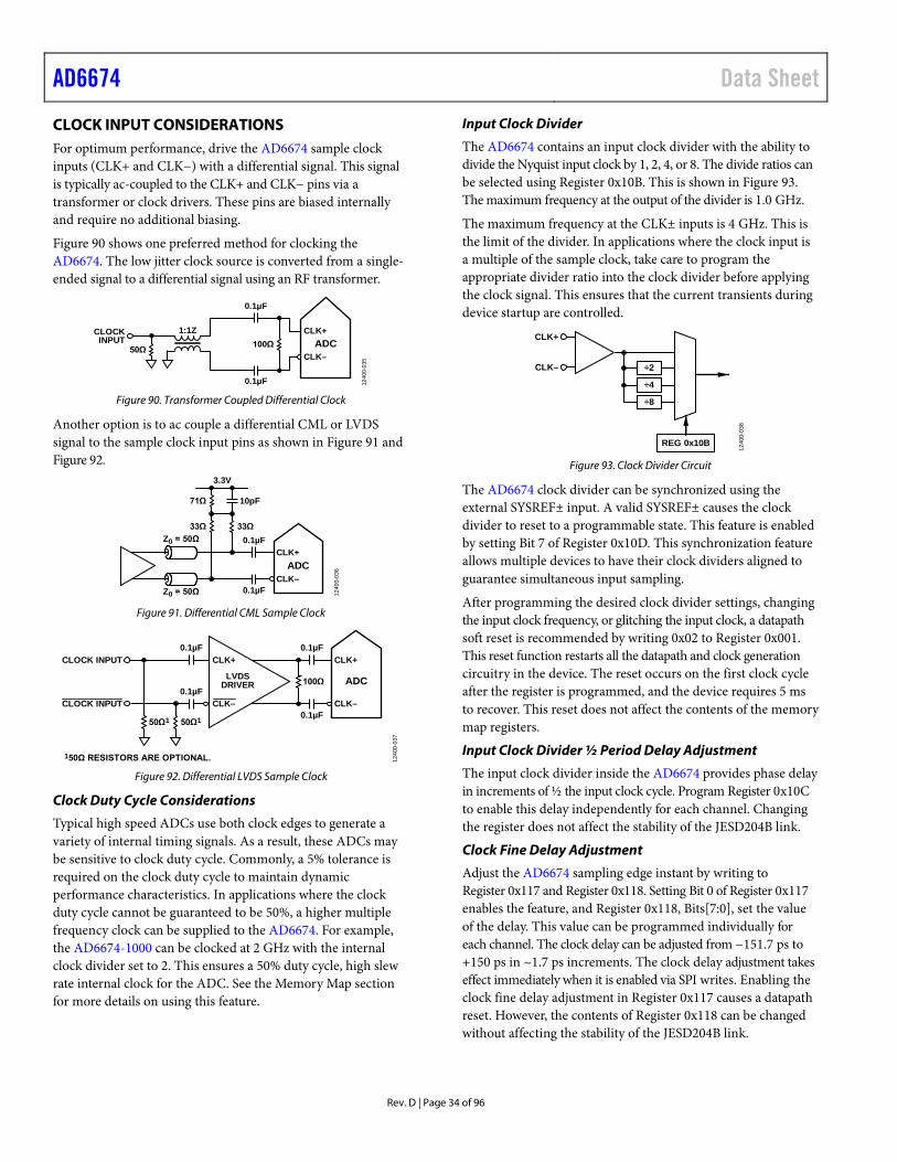
AD6674 Data Sheet
Rev. D | Page 34 of 96
CLOCK INPUT CONSIDERATIONS For optimum performance, drive the AD6674 sample clock inputs (CLK+ and CLK−) with a differential signal. This signal is typically ac-coupled to the CLK+ and CLK− pins via a transformer or clock drivers. These pins are biased internally and require no additional biasing.
Figure 90 shows one preferred method for clocking the AD6674. The low jitter clock source is converted from a single-ended signal to a differential signal using an RF transformer.
ADCCLK+
CLK–
0.1µF
0.1µF
100Ω50Ω
CLOCKINPUT
1:1Z
1240
0-03
5
Figure 90. Transformer Coupled Differential Clock
Another option is to ac couple a differential CML or LVDS signal to the sample clock input pins as shown in Figure 91 and Figure 92.
ADCCLK+
CLK–
0.1µF
0.1µF
Z0 = 50Ω
Z0 = 50Ω
33Ω 33Ω
71Ω 10pF
3.3V
1240
0-03
6
Figure 91. Differential CML Sample Clock
ADC
CLK+
CLK–
0.1µF
0.1µF
0.1µF
0.1µF
50Ω150Ω1
100Ω
CLOCK INPUT
LVDSDRIVER
CLK+
CLK–
150Ω RESISTORS ARE OPTIONAL.
CLOCK INPUT
1240
0-03
7
Figure 92. Differential LVDS Sample Clock
Clock Duty Cycle Considerations
Typical high speed ADCs use both clock edges to generate a variety of internal timing signals. As a result, these ADCs may be sensitive to clock duty cycle. Commonly, a 5% tolerance is required on the clock duty cycle to maintain dynamic performance characteristics. In applications where the clock duty cycle cannot be guaranteed to be 50%, a higher multiple frequency clock can be supplied to the AD6674. For example, the AD6674-1000 can be clocked at 2 GHz with the internal clock divider set to 2. This ensures a 50% duty cycle, high slew rate internal clock for the ADC. See the Memory Map section for more details on using this feature.
Input Clock Divider
The AD6674 contains an input clock divider with the ability to divide the Nyquist input clock by 1, 2, 4, or 8. The divide ratios can be selected using Register 0x10B. This is shown in Figure 93. The maximum frequency at the output of the divider is 1.0 GHz.
The maximum frequency at the CLK± inputs is 4 GHz. This is the limit of the divider. In applications where the clock input is a multiple of the sample clock, take care to program the appropriate divider ratio into the clock divider before applying the clock signal. This ensures that the current transients during device startup are controlled.
CLK+
CLK– ÷2
÷4
REG 0x10B
÷8
1240
0-03
8
Figure 93. Clock Divider Circuit
The AD6674 clock divider can be synchronized using the external SYSREF± input. A valid SYSREF± causes the clock divider to reset to a programmable state. This feature is enabled by setting Bit 7 of Register 0x10D. This synchronization feature allows multiple devices to have their clock dividers aligned to guarantee simultaneous input sampling.
After programming the desired clock divider settings, changing the input clock frequency, or glitching the input clock, a datapath soft reset is recommended by writing 0x02 to Register 0x001. This reset function restarts all the datapath and clock generation circuitry in the device. The reset occurs on the first clock cycle after the register is programmed, and the device requires 5 ms to recover. This reset does not affect the contents of the memory map registers.
Input Clock Divider ½ Period Delay Adjustment
The input clock divider inside the AD6674 provides phase delay in increments of ½ the input clock cycle. Program Register 0x10C to enable this delay independently for each channel. Changing the register does not affect the stability of the JESD204B link.
Clock Fine Delay Adjustment
Adjust the AD6674 sampling edge instant by writing to Register 0x117 and Register 0x118. Setting Bit 0 of Register 0x117 enables the feature, and Register 0x118, Bits[7:0], set the value of the delay. This value can be programmed individually for each channel. The clock delay can be adjusted from −151.7 ps to +150 ps in ~1.7 ps increments. The clock delay adjustment takes effect immediately when it is enabled via SPI writes. Enabling the clock fine delay adjustment in Register 0x117 causes a datapath reset. However, the contents of Register 0x118 can be changed without affecting the stability of the JESD204B link.
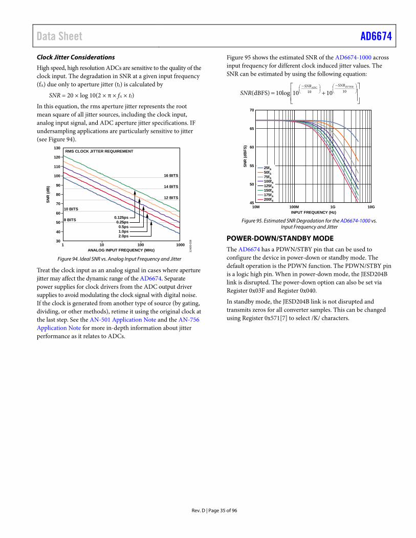
Data Sheet AD6674
Rev. D | Page 35 of 96
Clock Jitter Considerations
High speed, high resolution ADCs are sensitive to the quality of the clock input. The degradation in SNR at a given input frequency (fA) due only to aperture jitter (tJ) is calculated by
SNR = 20 × log 10(2 × π × fA × tJ)
In this equation, the rms aperture jitter represents the root mean square of all jitter sources, including the clock input, analog input signal, and ADC aperture jitter specifications. IF undersampling applications are particularly sensitive to jitter (see Figure 94).
1 10 100 100030
40
50
60
70
80
90
100
110
120
130
0.125ps0.25ps
0.5ps1.0ps2.0ps
10 BITS
16 BITS
14 BITS
12 BITS
8 BITS
RMS CLOCK JITTER REQUIREMENT
SNR
(dB
)
ANALOG INPUT FREQUENCY (MHz) 1240
0-03
9
Figure 94. Ideal SNR vs. Analog Input Frequency and Jitter
Treat the clock input as an analog signal in cases where aperture jitter may affect the dynamic range of the AD6674. Separate power supplies for clock drivers from the ADC output driver supplies to avoid modulating the clock signal with digital noise. If the clock is generated from another type of source (by gating, dividing, or other methods), retime it using the original clock at the last step. See the AN-501 Application Note and the AN-756 Application Note for more in-depth information about jitter performance as it relates to ADCs.
Figure 95 shows the estimated SNR of the AD6674-1000 across input frequency for different clock induced jitter values. The SNR can be estimated by using the following equation:
+=
−
−
1010 101010log(dBFS)JITTERADC
SNRSNR
SNR
SNR
(dB
FS)
INPUT FREQUENCY (Hz)
45
50
55
60
65
70
10M 100M 1G 10G
25fs50fs75fs100fs125fs150fs175fs200fs
Figure 95. Estimated SNR Degradation for the AD6674-1000 vs.
Input Frequency and Jitter
POWER-DOWN/STANDBY MODE The AD6674 has a PDWN/STBY pin that can be used to configure the device in power-down or standby mode. The default operation is the PDWN function. The PDWN/STBY pin is a logic high pin. When in power-down mode, the JESD204B link is disrupted. The power-down option can also be set via Register 0x03F and Register 0x040.
In standby mode, the JESD204B link is not disrupted and transmits zeros for all converter samples. This can be changed using Register 0x571[7] to select /K/ characters.
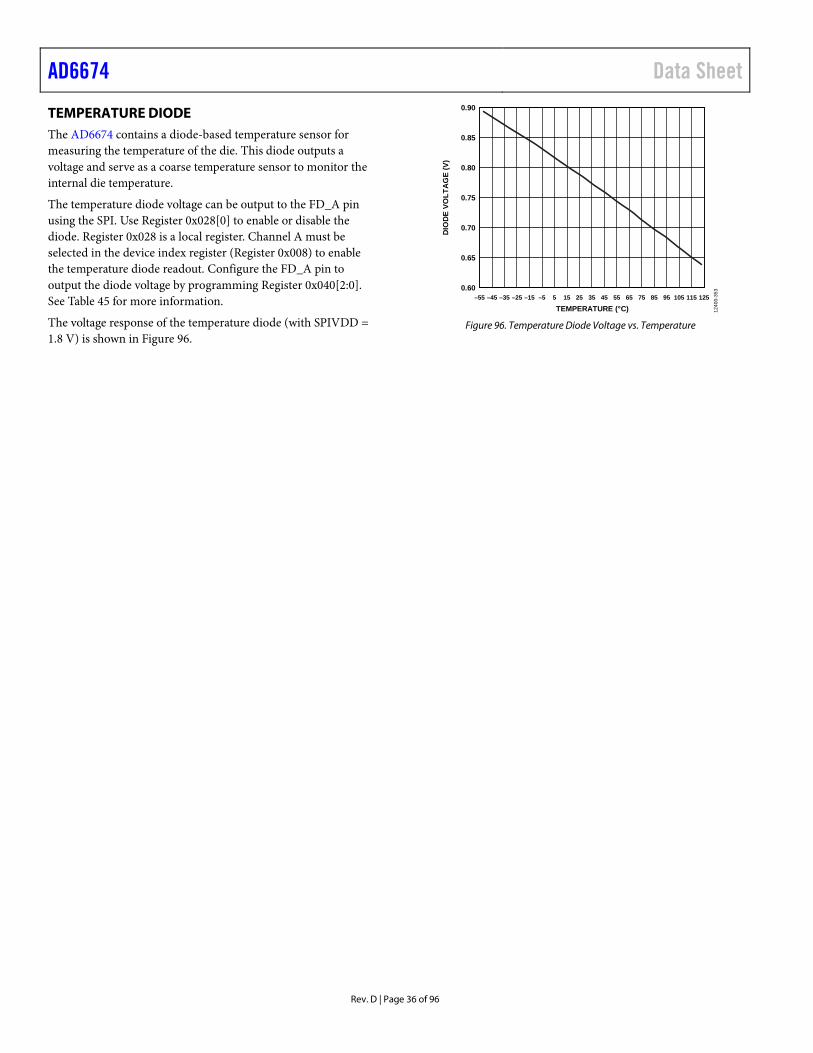
AD6674 Data Sheet
Rev. D | Page 36 of 96
TEMPERATURE DIODE The AD6674 contains a diode-based temperature sensor for measuring the temperature of the die. This diode outputs a voltage and serve as a coarse temperature sensor to monitor the internal die temperature.
The temperature diode voltage can be output to the FD_A pin using the SPI. Use Register 0x028[0] to enable or disable the diode. Register 0x028 is a local register. Channel A must be selected in the device index register (Register 0x008) to enable the temperature diode readout. Configure the FD_A pin to output the diode voltage by programming Register 0x040[2:0]. See Table 45 for more information.
The voltage response of the temperature diode (with SPIVDD = 1.8 V) is shown in Figure 96.
DIO
DE
VOLT
AG
E (V
)
TEMPERATURE (°C)
0.60
0.65
0.70
0.75
0.80
0.85
0.90
1240
0-35
3
–55 –45 –35 –25 –15 –5 5 15 25 35 45 55 65 75 85 95 105 115 125
Figure 96. Temperature Diode Voltage vs. Temperature
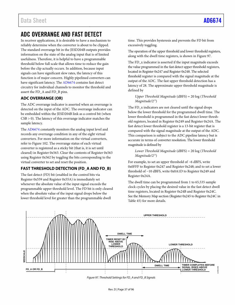
Data Sheet AD6674
Rev. D | Page 37 of 96
ADC OVERRANGE AND FAST DETECT In receiver applications, it is desirable to have a mechanism to reliably determine when the converter is about to be clipped. The standard overrange bit in the JESD204B outputs provides information on the state of the analog input that is of limited usefulness. Therefore, it is helpful to have a programmable threshold below full scale that allows time to reduce the gain before the clip actually occurs. In addition, because input signals can have significant slew rates, the latency of this function is of major concern. Highly pipelined converters can have significant latency. The AD6674 contains fast detect circuitry for individual channels to monitor the threshold and assert the FD_A and FD_B pins.
ADC OVERRANGE (OR) The ADC overrange indicator is asserted when an overrange is detected on the input of the ADC. The overrange indicator can be embedded within the JESD204B link as a control bit (when CSB > 0). The latency of this overrange indicator matches the sample latency.
The AD6674 constantly monitors the analog input level and records any overrange condition in any of the eight virtual converters. For more information on the virtual converters, refer to Figure 102. The overrange status of each virtual converter is registered as a sticky bit (that is, it is set until cleared) in Register 0x563. Clear the contents of Register 0x563 using Register 0x562 by toggling the bits corresponding to the virtual converter to set and reset the position.
FAST THRESHOLD DETECTION (FD_A AND FD_B) The fast detect (FD) bit (enabled in the control bits via Register 0x559 and Register 0x55A) is immediately set whenever the absolute value of the input signal exceeds the programmable upper threshold level. The FD bit is only cleared when the absolute value of the input signal drops below the lower threshold level for greater than the programmable dwell
time. This provides hysteresis and prevents the FD bit from excessively toggling.
The operation of the upper threshold and lower threshold registers, along with the dwell time registers, is shown in Figure 97.
The FD_x indicator is asserted if the input magnitude exceeds the value programmed in the fast detect upper threshold registers, located in Register 0x247 and Register 0x248. The selected threshold register is compared with the signal magnitude at the output of the ADC. The fast upper threshold detection has a latency of 28. The approximate upper threshold magnitude is defined by
Upper Threshold Magnitude (dBFS) = 20 log (Threshold Magnitude/213)
The FD_x indicators are not cleared until the signal drops below the lower threshold for the programmed dwell time. The lower threshold is programmed in the fast detect lower thresh-old registers, located in Register 0x249 and Register 0x24A. The fast detect lower threshold register is a 13-bit register that is compared with the signal magnitude at the output of the ADC. This comparison is subject to the ADC pipeline latency but is accurate in terms of converter resolution. The lower threshold magnitude is defined by
Lower Threshold Magnitude (dBFS) = 20 log (Threshold Magnitude/213)
For example, to set an upper threshold of −6 dBFS, write 0x0FFF to Register 0x247 and Register 0x248; and to set a lower threshold of −10 dBFS, write 0x0A1D to Register 0x249 and Register 0x24A.
The dwell time can be programmed from 1 to 65,535 sample clock cycles by placing the desired value in the fast detect dwell time registers, located in Register 0x24B and Register 0x24C. See the Memory Map section (Register 0x245 to Register 0x24C in Table 45) for more details.
UPPER THRESHOLD
LOWER THRESHOLD
FD_A OR FD_B
MID
SCA
LE
DWELL TIME
TIMER RESET BYRISE ABOVE
LOWERTHRESHOLD
TIMER COMPLETES BEFORESIGNAL RISES ABOVELOWER THRESHOLD
DWELL TIME
1240
0-04
0
Figure 97. Threshold Settings for FD_A and FD_B Signals
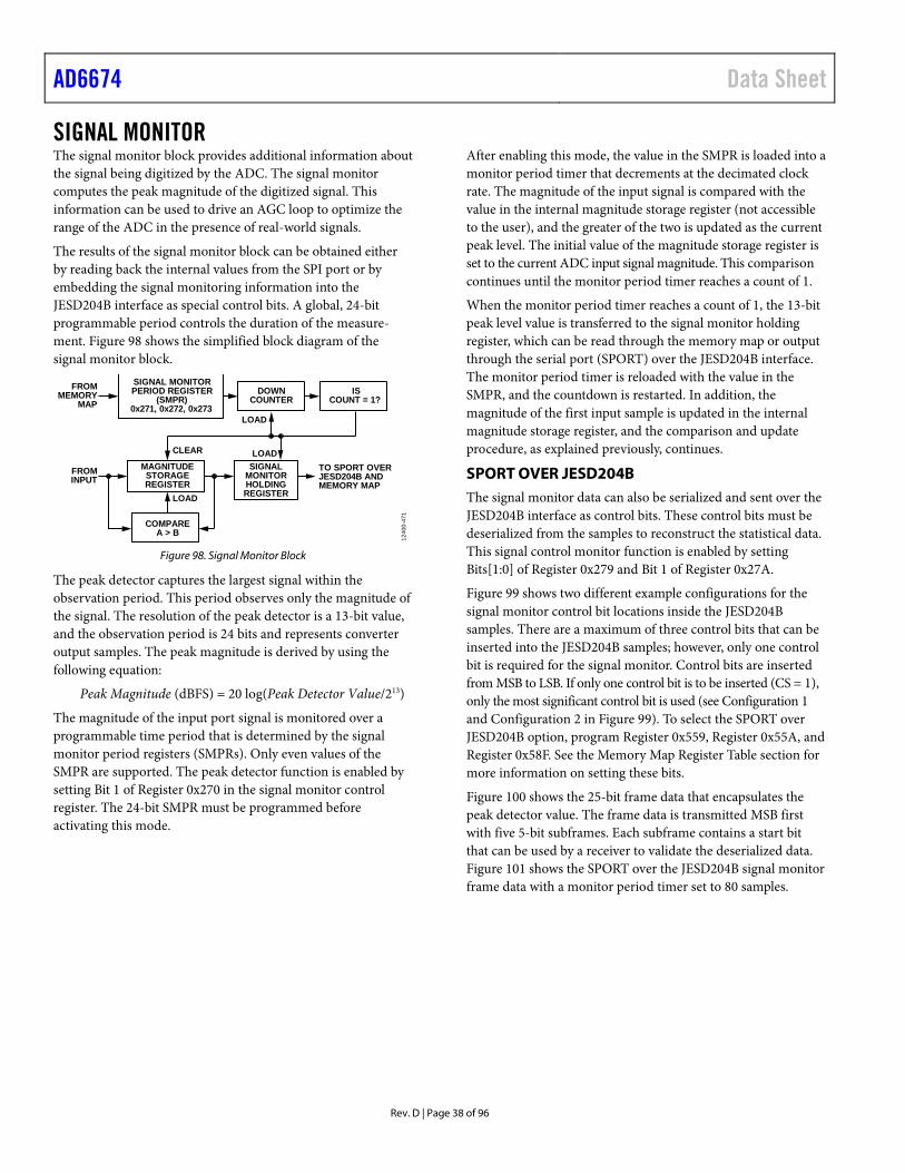
AD6674 Data Sheet
Rev. D | Page 38 of 96
SIGNAL MONITOR The signal monitor block provides additional information about the signal being digitized by the ADC. The signal monitor computes the peak magnitude of the digitized signal. This information can be used to drive an AGC loop to optimize the range of the ADC in the presence of real-world signals.
The results of the signal monitor block can be obtained either by reading back the internal values from the SPI port or by embedding the signal monitoring information into the JESD204B interface as special control bits. A global, 24-bit programmable period controls the duration of the measure-ment. Figure 98 shows the simplified block diagram of the signal monitor block.
FROMMEMORY
MAPDOWN
COUNTERIS
COUNT = 1?
MAGNITUDESTORAGEREGISTER
FROMINPUT
SIGNALMONITORHOLDINGREGISTER
LOAD
CLEAR
COMPAREA > B
LOAD
LOADTO SPORT OVERJESD204B ANDMEMORY MAP
SIGNAL MONITORPERIOD REGISTER
(SMPR)0x271, 0x272, 0x273
1240
0-47
1
Figure 98. Signal Monitor Block
The peak detector captures the largest signal within the observation period. This period observes only the magnitude of the signal. The resolution of the peak detector is a 13-bit value, and the observation period is 24 bits and represents converter output samples. The peak magnitude is derived by using the following equation:
Peak Magnitude (dBFS) = 20 log(Peak Detector Value/213)
The magnitude of the input port signal is monitored over a programmable time period that is determined by the signal monitor period registers (SMPRs). Only even values of the SMPR are supported. The peak detector function is enabled by setting Bit 1 of Register 0x270 in the signal monitor control register. The 24-bit SMPR must be programmed before activating this mode.
After enabling this mode, the value in the SMPR is loaded into a monitor period timer that decrements at the decimated clock rate. The magnitude of the input signal is compared with the value in the internal magnitude storage register (not accessible to the user), and the greater of the two is updated as the current peak level. The initial value of the magnitude storage register is set to the current ADC input signal magnitude. This comparison continues until the monitor period timer reaches a count of 1.
When the monitor period timer reaches a count of 1, the 13-bit peak level value is transferred to the signal monitor holding register, which can be read through the memory map or output through the serial port (SPORT) over the JESD204B interface. The monitor period timer is reloaded with the value in the SMPR, and the countdown is restarted. In addition, the magnitude of the first input sample is updated in the internal magnitude storage register, and the comparison and update procedure, as explained previously, continues.
SPORT OVER JESD204B The signal monitor data can also be serialized and sent over the JESD204B interface as control bits. These control bits must be deserialized from the samples to reconstruct the statistical data. This signal control monitor function is enabled by setting Bits[1:0] of Register 0x279 and Bit 1 of Register 0x27A.
Figure 99 shows two different example configurations for the signal monitor control bit locations inside the JESD204B samples. There are a maximum of three control bits that can be inserted into the JESD204B samples; however, only one control bit is required for the signal monitor. Control bits are inserted from MSB to LSB. If only one control bit is to be inserted (CS = 1), only the most significant control bit is used (see Configuration 1 and Configuration 2 in Figure 99). To select the SPORT over JESD204B option, program Register 0x559, Register 0x55A, and Register 0x58F. See the Memory Map Register Table section for more information on setting these bits.
Figure 100 shows the 25-bit frame data that encapsulates the peak detector value. The frame data is transmitted MSB first with five 5-bit subframes. Each subframe contains a start bit that can be used by a receiver to validate the deserialized data. Figure 101 shows the SPORT over the JESD204B signal monitor frame data with a monitor period timer set to 80 samples.
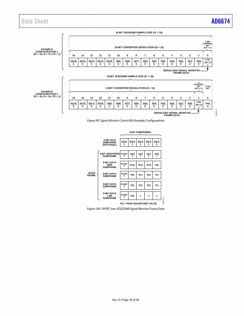
Data Sheet AD6674
Rev. D | Page 39 of 96
15
14-BIT CONVERTER RESOLUTION (N = 14)
TAILX
1CONTROL
BIT(CS = 1)
1-BITCONTROL
BIT(CS = 1)
14 13 12 11 10 9 8 7 6 5 4 3 2 1 0
15 14 13 12 11 10 9 8 7 6 5 4 3 2 1 0
1 TAILBIT
SERIALIZED SIGNAL MONITORFRAME DATA
EXAMPLECONFIGURATION 1
(N' = 16, N = 15, CS = 1)
EXAMPLECONFIGURATION 2
(N' = 16, N = 14, CS = 1)
SERIALIZED SIGNAL MONITORFRAME DATA
16-BIT JESD204B SAMPLE SIZE (N' = 16)
S[13]X
S[12]X
S[11]X
S[10]X
S[9]X
S[8]X
S[7]X
S[6]X
S[5]X
S[4]X
S[3]X
S[2]X
S[1]X
S[0]X
CTRL[BIT 2]
X
CTRL[BIT 2]
X
S[14]X
S[13]X
S[12]X
S[11]X
S[10]X
S[9]X
S[8]X
S[7]X
S[6]X
S[5]X
S[4]X
S[3]X
S[2]X
S[1]X
S[0]X
15-BIT CONVERTER RESOLUTION (N = 15)
16-BIT JESD204B SAMPLE SIZE (N' = 16)
1240
0-47
2
Figure 99. Signal Monitor Control Bit Example Configurations
25-BITFRAME
5-BIT IDLESUBFRAME(OPTIONAL)
5-BIT IDENTIFIERSUBFRAME
5-BIT DATAMSB
SUBFRAME
5-BIT DATASUBFRAME
5-BIT DATASUBFRAME
5-BIT DATALSB
SUBFRAME
5-BIT SUBFRAMES
P[] = PEAK MAGNITUDE VALUE
IDLE1
IDLE1
IDLE1
IDLE1
IDLE1
START0 P[0] 0 0 0
START0 P[4] P[3] P[2] P1]
START0 P[8] P[7] P[6] P5]
START0 P[12] P[11] P[10] P[9]
START0
ID[3]0
ID[2]0
ID[1]0
ID[0]1
1240
0-47
3
Figure 100. SPORT over JESD204B Signal Monitor Frame Data
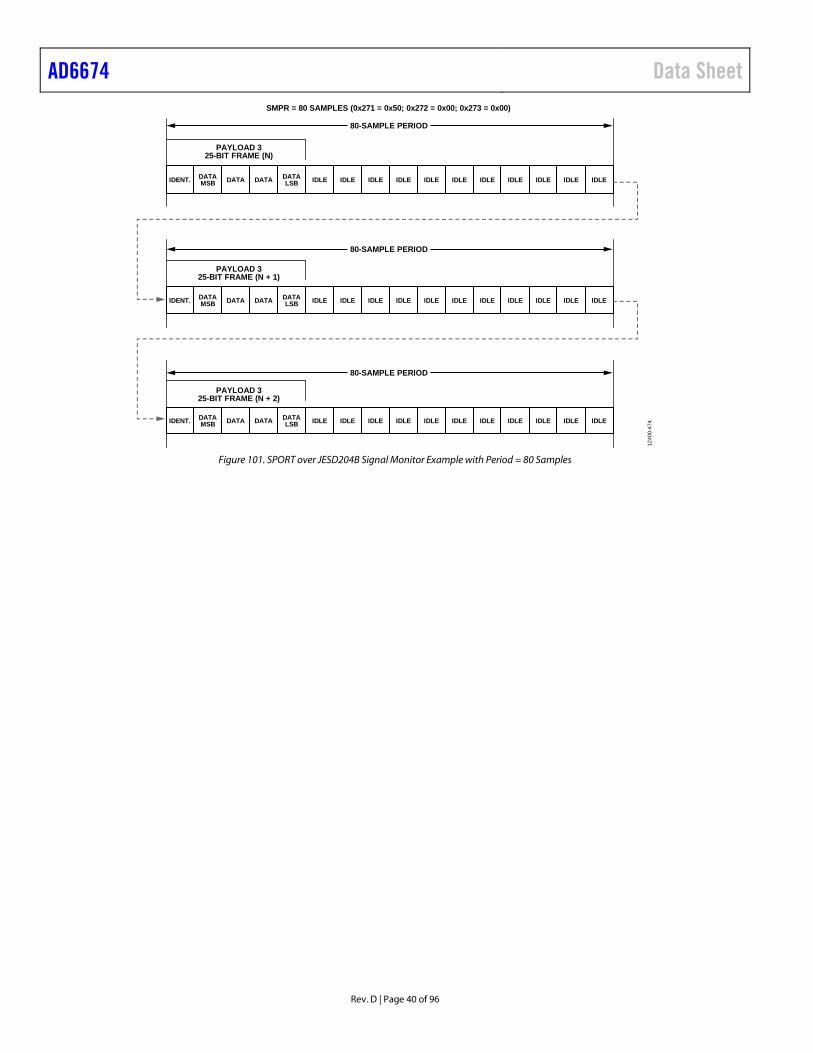
AD6674 Data Sheet
Rev. D | Page 40 of 96
PAYLOAD 325-BIT FRAME (N)
PAYLOAD 325-BIT FRAME (N + 1)
PAYLOAD 325-BIT FRAME (N + 2)
IDLE IDLE IDLE IDLE IDLE IDLEIDLE IDLE IDLE IDLE IDLEIDENT. DATAMSB DATA DATA DATA
LSB
IDLE IDLE IDLE IDLE IDLE IDLEIDLE IDLE IDLE IDLE IDLEIDENT. DATAMSB DATA DATA DATA
LSB
IDLE IDLE IDLE IDLE IDLE IDLEIDLE IDLE IDLE IDLE IDLEIDENT. DATAMSB DATA DATA DATA
LSB
SMPR = 80 SAMPLES (0x271 = 0x50; 0x272 = 0x00; 0x273 = 0x00)
80-SAMPLE PERIOD
80-SAMPLE PERIOD
80-SAMPLE PERIOD
1240
0-47
4
Figure 101. SPORT over JESD204B Signal Monitor Example with Period = 80 Samples
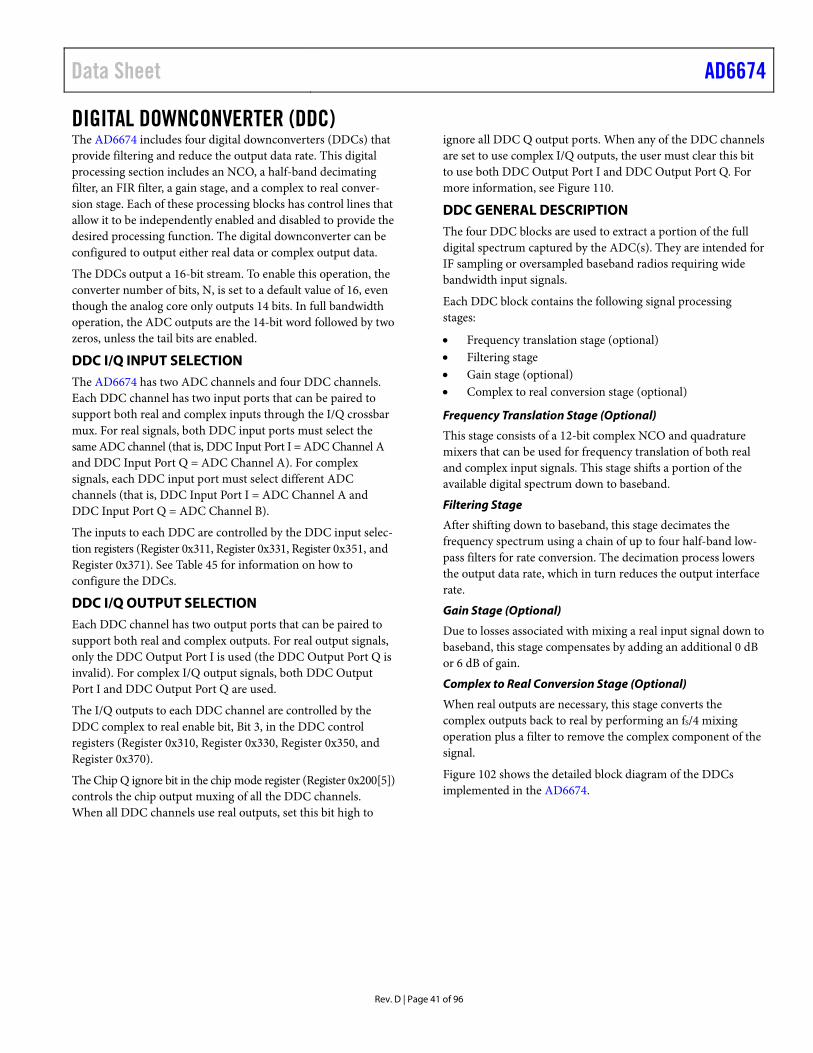
Data Sheet AD6674
Rev. D | Page 41 of 96
DIGITAL DOWNCONVERTER (DDC) The AD6674 includes four digital downconverters (DDCs) that provide filtering and reduce the output data rate. This digital processing section includes an NCO, a half-band decimating filter, an FIR filter, a gain stage, and a complex to real conver-sion stage. Each of these processing blocks has control lines that allow it to be independently enabled and disabled to provide the desired processing function. The digital downconverter can be configured to output either real data or complex output data.
The DDCs output a 16-bit stream. To enable this operation, the converter number of bits, N, is set to a default value of 16, even though the analog core only outputs 14 bits. In full bandwidth operation, the ADC outputs are the 14-bit word followed by two zeros, unless the tail bits are enabled.
DDC I/Q INPUT SELECTION The AD6674 has two ADC channels and four DDC channels. Each DDC channel has two input ports that can be paired to support both real and complex inputs through the I/Q crossbar mux. For real signals, both DDC input ports must select the same ADC channel (that is, DDC Input Port I = ADC Channel A and DDC Input Port Q = ADC Channel A). For complex signals, each DDC input port must select different ADC channels (that is, DDC Input Port I = ADC Channel A and DDC Input Port Q = ADC Channel B).
The inputs to each DDC are controlled by the DDC input selec-tion registers (Register 0x311, Register 0x331, Register 0x351, and Register 0x371). See Table 45 for information on how to configure the DDCs.
DDC I/Q OUTPUT SELECTION Each DDC channel has two output ports that can be paired to support both real and complex outputs. For real output signals, only the DDC Output Port I is used (the DDC Output Port Q is invalid). For complex I/Q output signals, both DDC Output Port I and DDC Output Port Q are used.
The I/Q outputs to each DDC channel are controlled by the DDC complex to real enable bit, Bit 3, in the DDC control registers (Register 0x310, Register 0x330, Register 0x350, and Register 0x370).
The Chip Q ignore bit in the chip mode register (Register 0x200[5]) controls the chip output muxing of all the DDC channels. When all DDC channels use real outputs, set this bit high to
ignore all DDC Q output ports. When any of the DDC channels are set to use complex I/Q outputs, the user must clear this bit to use both DDC Output Port I and DDC Output Port Q. For more information, see Figure 110.
DDC GENERAL DESCRIPTION The four DDC blocks are used to extract a portion of the full digital spectrum captured by the ADC(s). They are intended for IF sampling or oversampled baseband radios requiring wide bandwidth input signals.
Each DDC block contains the following signal processing stages:
• Frequency translation stage (optional) • Filtering stage • Gain stage (optional) • Complex to real conversion stage (optional)
Frequency Translation Stage (Optional) This stage consists of a 12-bit complex NCO and quadrature mixers that can be used for frequency translation of both real and complex input signals. This stage shifts a portion of the available digital spectrum down to baseband.
Filtering Stage
After shifting down to baseband, this stage decimates the frequency spectrum using a chain of up to four half-band low-pass filters for rate conversion. The decimation process lowers the output data rate, which in turn reduces the output interface rate.
Gain Stage (Optional)
Due to losses associated with mixing a real input signal down to baseband, this stage compensates by adding an additional 0 dB or 6 dB of gain.
Complex to Real Conversion Stage (Optional)
When real outputs are necessary, this stage converts the complex outputs back to real by performing an fS/4 mixing operation plus a filter to remove the complex component of the signal.
Figure 102 shows the detailed block diagram of the DDCs implemented in the AD6674.
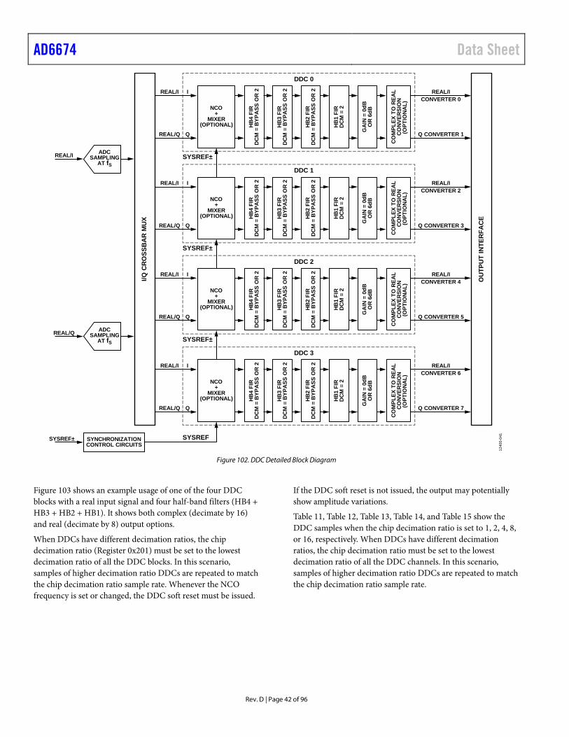
AD6674 Data Sheet
Rev. D | Page 42 of 96
NCO+
MIXER(OPTIONAL)
CO
MPL
EX T
O R
EAL
CO
NVE
RSI
ON
(OPT
ION
AL)
HB
4 FI
RD
CM
= B
YPA
SS O
R 2
HB
3 FI
RD
CM
= B
YPA
SS O
R 2
HB
2 FI
RD
CM
= B
YPA
SS O
R 2
HB
1 FI
RD
CM
= 2
GA
IN =
0dB
OR
6dB
DDC 3
SYSREF
REAL/I
REAL/Q
REAL/ICONVERTER 6
Q CONVERTER 7
I
Q
NCO+
MIXER(OPTIONAL)
CO
MPL
EX T
O R
EAL
CO
NVE
RSI
ON
(OPT
ION
AL)
HB
4 FI
RD
CM
= B
YPA
SS O
R 2
HB
3 FI
RD
CM
= B
YPA
SS O
R 2
HB
2 FI
RD
CM
= B
YPA
SS O
R 2
HB
1 FI
RD
CM
= 2
GA
IN =
0dB
OR
6dB
DDC 0
SYSREF±
REAL/I
REAL/Q
REAL/ICONVERTER 0
Q CONVERTER 1
I
Q
NCO+
MIXER(OPTIONAL)
CO
MPL
EX T
O R
EAL
CO
NVE
RSI
ON
(OPT
ION
AL)
HB
4 FI
RD
CM
= B
YPA
SS O
R 2
HB
3 FI
RD
CM
= B
YPA
SS O
R 2
HB
2 FI
RD
CM
= B
YPA
SS O
R 2
HB
1 FI
RD
CM
= 2
GA
IN =
0dB
OR
6dB
DDC 1
SYSREF±
REAL/I
REAL/Q
REAL/ICONVERTER 2
Q CONVERTER 3
I
Q
NCO+
MIXER(OPTIONAL)
CO
MPL
EX T
O R
EAL
CO
NVE
RSI
ON
(OPT
ION
AL)
HB
4 FI
RD
CM
= B
YPA
SS O
R 2
HB
3 FI
RD
CM
= B
YPA
SS O
R 2
HB
2 FI
RD
CM
= B
YPA
SS O
R 2
HB
1 FI
RD
CM
= 2
GA
IN =
0dB
OR
6dB
DDC 2
SYSREF±
REAL/I
REAL/Q
REAL/ICONVERTER 4
Q CONVERTER 5
I
Q
OU
TPU
T IN
TER
FAC
E
I/Q C
RO
SSB
AR
MU
XADC
SAMPLINGAT fS
REAL/I
ADCSAMPLING
AT fS
REAL/Q
SYNCHRONIZATIONCONTROL CIRCUITS
SYSREF±
1240
0-04
1
Figure 102. DDC Detailed Block Diagram
Figure 103 shows an example usage of one of the four DDC blocks with a real input signal and four half-band filters (HB4 + HB3 + HB2 + HB1). It shows both complex (decimate by 16) and real (decimate by 8) output options.
When DDCs have different decimation ratios, the chip decimation ratio (Register 0x201) must be set to the lowest decimation ratio of all the DDC blocks. In this scenario, samples of higher decimation ratio DDCs are repeated to match the chip decimation ratio sample rate. Whenever the NCO frequency is set or changed, the DDC soft reset must be issued.
If the DDC soft reset is not issued, the output may potentially show amplitude variations.
Table 11, Table 12, Table 13, Table 14, and Table 15 show the DDC samples when the chip decimation ratio is set to 1, 2, 4, 8, or 16, respectively. When DDCs have different decimation ratios, the chip decimation ratio must be set to the lowest decimation ratio of all the DDC channels. In this scenario, samples of higher decimation ratio DDCs are repeated to match the chip decimation ratio sample rate.
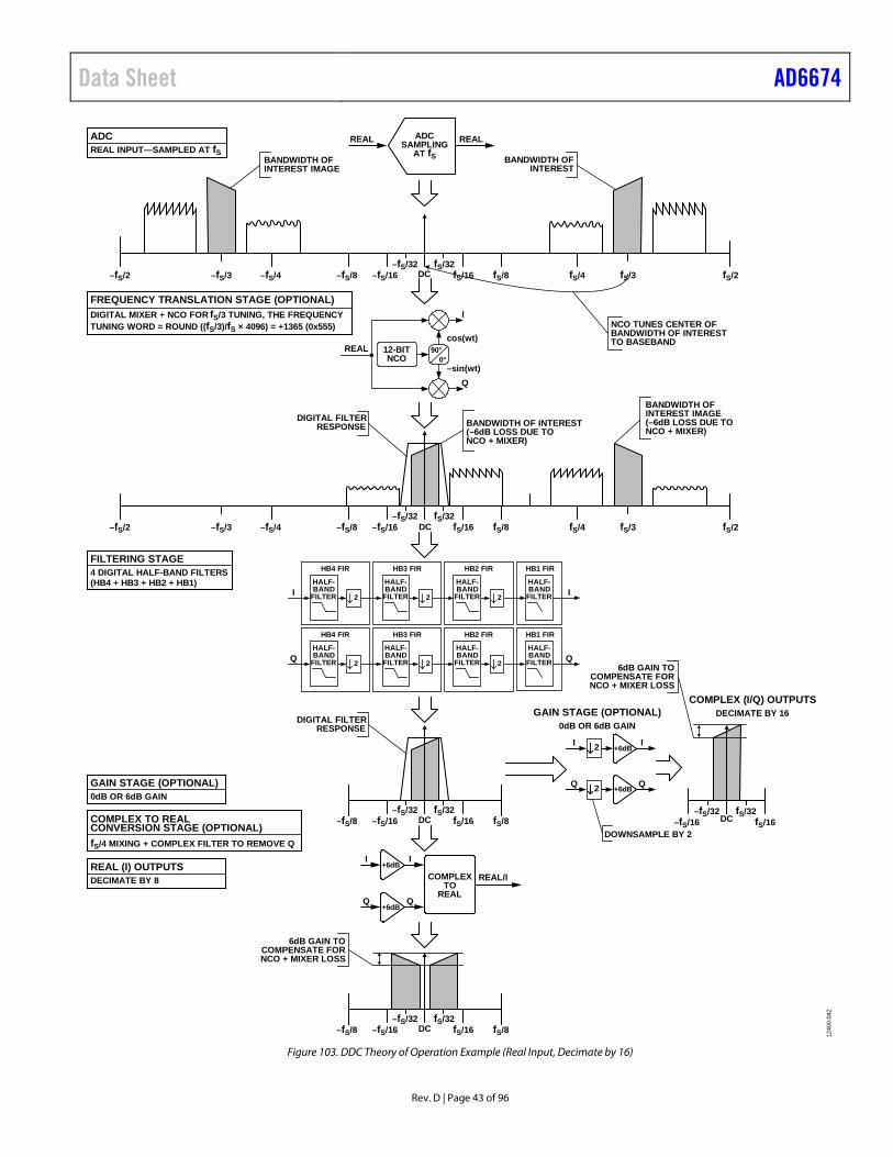
Data Sheet AD6674
Rev. D | Page 43 of 96
cos(wt)
0°90°
I
Q
REAL
BANDWIDTH OFINTEREST
BANDWIDTH OFINTEREST IMAGE
DIGITAL FILTERRESPONSE
DC
DC
ADCSAMPLING
AT fS
REAL REAL
HALF-BAND
FILTER
HB4 FIR
2
HALF-BAND
FILTER
HB3 FIR
2
HALF-BAND
FILTER
HB2 FIR
2
HALF-BAND
FILTER
HB1 FIR
I I
HALF-BAND
FILTER
HB4 FIR
2
HALF-BAND
FILTER
HB3 FIR
2
HALF-BAND
FILTER
HB2 FIR
2
HALF-BAND
FILTER
HB1 FIR
Q Q
ADCREAL INPUT—SAMPLED AT fS
FILTERING STAGE4 DIGITAL HALF-BAND FILTERS(HB4 + HB3 + HB2 + HB1)
FREQUENCY TRANSLATION STAGE (OPTIONAL)DIGITAL MIXER + NCO FOR fS/3 TUNING, THE FREQUENCYTUNING WORD = ROUND ((fS/3)/fS × 4096) = +1365 (0x555) NCO TUNES CENTER OF
BANDWIDTH OF INTERESTTO BASEBAND
BANDWIDTH OFINTEREST IMAGE(–6dB LOSS DUE TONCO + MIXER)
BANDWIDTH OF INTEREST(–6dB LOSS DUE TONCO + MIXER)
–fS/2 –fS/3 –fS/4 –fS/8 fS/16 fS/8 fS/4 fS/3 fS/2–fS/16–fS/32 fS/32
–fS/2 –fS/3 –fS/4 –fS/8 fS/16 fS/8 fS/4 fS/3 fS/2–fS/16–fS/32 fS/32
–sin(wt)
12-BITNCO
DC
DIGITAL FILTERRESPONSE
DCDC
I
Q
I
Q
2
2
I
Q
REAL/ICOMPLEXTO
REAL
I
Q
GAIN STAGE (OPTIONAL)0dB OR 6dB GAIN
COMPLEX (I/Q) OUTPUTSDECIMATE BY 16
GAIN STAGE (OPTIONAL)0dB OR 6dB GAIN
REAL (I) OUTPUTSDECIMATE BY 8
COMPLEX TO REALCONVERSION STAGE (OPTIONAL)fS/4 MIXING + COMPLEX FILTER TO REMOVE Q
–fS/8 fS/16 fS/8–fS/16–fS/32 fS/32
–fS/8 fS/16 fS/8–fS/16–fS/32 fS/32
fS/16–fS/16–fS/32 fS/32
6dB GAIN TOCOMPENSATE FORNCO + MIXER LOSS
6dB GAIN TOCOMPENSATE FORNCO + MIXER LOSS
DOWNSAMPLE BY 2
+6dB
+6dB
+6dB
+6dB
1240
0-04
2
Figure 103. DDC Theory of Operation Example (Real Input, Decimate by 16)
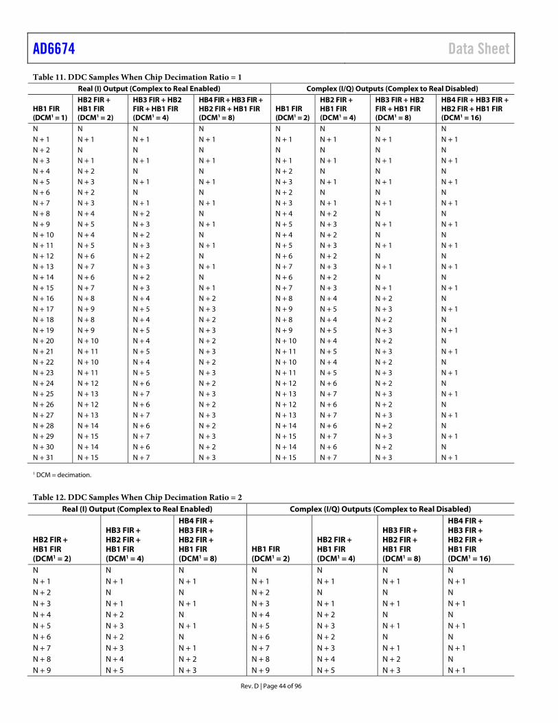
AD6674 Data Sheet
Rev. D | Page 44 of 96
Table 11. DDC Samples When Chip Decimation Ratio = 1 Real (I) Output (Complex to Real Enabled) Complex (I/Q) Outputs (Complex to Real Disabled)
HB1 FIR (DCM1 = 1)
HB2 FIR + HB1 FIR (DCM1 = 2)
HB3 FIR + HB2 FIR + HB1 FIR (DCM1 = 4)
HB4 FIR + HB3 FIR + HB2 FIR + HB1 FIR (DCM1 = 8)
HB1 FIR (DCM1 = 2)
HB2 FIR + HB1 FIR (DCM1 = 4)
HB3 FIR + HB2 FIR + HB1 FIR (DCM1 = 8)
HB4 FIR + HB3 FIR + HB2 FIR + HB1 FIR (DCM1 = 16)
N N N N N N N N N + 1 N + 1 N + 1 N + 1 N + 1 N + 1 N + 1 N + 1 N + 2 N N N N N N N N + 3 N + 1 N + 1 N + 1 N + 1 N + 1 N + 1 N + 1 N + 4 N + 2 N N N + 2 N N N N + 5 N + 3 N + 1 N + 1 N + 3 N + 1 N + 1 N + 1 N + 6 N + 2 N N N + 2 N N N N + 7 N + 3 N + 1 N + 1 N + 3 N + 1 N + 1 N + 1 N + 8 N + 4 N + 2 N N + 4 N + 2 N N N + 9 N + 5 N + 3 N + 1 N + 5 N + 3 N + 1 N + 1 N + 10 N + 4 N + 2 N N + 4 N + 2 N N N + 11 N + 5 N + 3 N + 1 N + 5 N + 3 N + 1 N + 1 N + 12 N + 6 N + 2 N N + 6 N + 2 N N N + 13 N + 7 N + 3 N + 1 N + 7 N + 3 N + 1 N + 1 N + 14 N + 6 N + 2 N N + 6 N + 2 N N N + 15 N + 7 N + 3 N + 1 N + 7 N + 3 N + 1 N + 1 N + 16 N + 8 N + 4 N + 2 N + 8 N + 4 N + 2 N N + 17 N + 9 N + 5 N + 3 N + 9 N + 5 N + 3 N + 1 N + 18 N + 8 N + 4 N + 2 N + 8 N + 4 N + 2 N N + 19 N + 9 N + 5 N + 3 N + 9 N + 5 N + 3 N + 1 N + 20 N + 10 N + 4 N + 2 N + 10 N + 4 N + 2 N N + 21 N + 11 N + 5 N + 3 N + 11 N + 5 N + 3 N + 1 N + 22 N + 10 N + 4 N + 2 N + 10 N + 4 N + 2 N N + 23 N + 11 N + 5 N + 3 N + 11 N + 5 N + 3 N + 1 N + 24 N + 12 N + 6 N + 2 N + 12 N + 6 N + 2 N N + 25 N + 13 N + 7 N + 3 N + 13 N + 7 N + 3 N + 1 N + 26 N + 12 N + 6 N + 2 N + 12 N + 6 N + 2 N N + 27 N + 13 N + 7 N + 3 N + 13 N + 7 N + 3 N + 1 N + 28 N + 14 N + 6 N + 2 N + 14 N + 6 N + 2 N N + 29 N + 15 N + 7 N + 3 N + 15 N + 7 N + 3 N + 1 N + 30 N + 14 N + 6 N + 2 N + 14 N + 6 N + 2 N N + 31 N + 15 N + 7 N + 3 N + 15 N + 7 N + 3 N + 1 1 DCM = decimation.
Table 12. DDC Samples When Chip Decimation Ratio = 2 Real (I) Output (Complex to Real Enabled) Complex (I/Q) Outputs (Complex to Real Disabled)
HB2 FIR + HB1 FIR (DCM1 = 2)
HB3 FIR + HB2 FIR + HB1 FIR (DCM1 = 4)
HB4 FIR + HB3 FIR + HB2 FIR + HB1 FIR (DCM1 = 8)
HB1 FIR (DCM1 = 2)
HB2 FIR + HB1 FIR (DCM1 = 4)
HB3 FIR + HB2 FIR + HB1 FIR (DCM1 = 8)
HB4 FIR + HB3 FIR + HB2 FIR + HB1 FIR (DCM1 = 16)
N N N N N N N N + 1 N + 1 N + 1 N + 1 N + 1 N + 1 N + 1 N + 2 N N N + 2 N N N N + 3 N + 1 N + 1 N + 3 N + 1 N + 1 N + 1 N + 4 N + 2 N N + 4 N + 2 N N N + 5 N + 3 N + 1 N + 5 N + 3 N + 1 N + 1 N + 6 N + 2 N N + 6 N + 2 N N N + 7 N + 3 N + 1 N + 7 N + 3 N + 1 N + 1 N + 8 N + 4 N + 2 N + 8 N + 4 N + 2 N N + 9 N + 5 N + 3 N + 9 N + 5 N + 3 N + 1
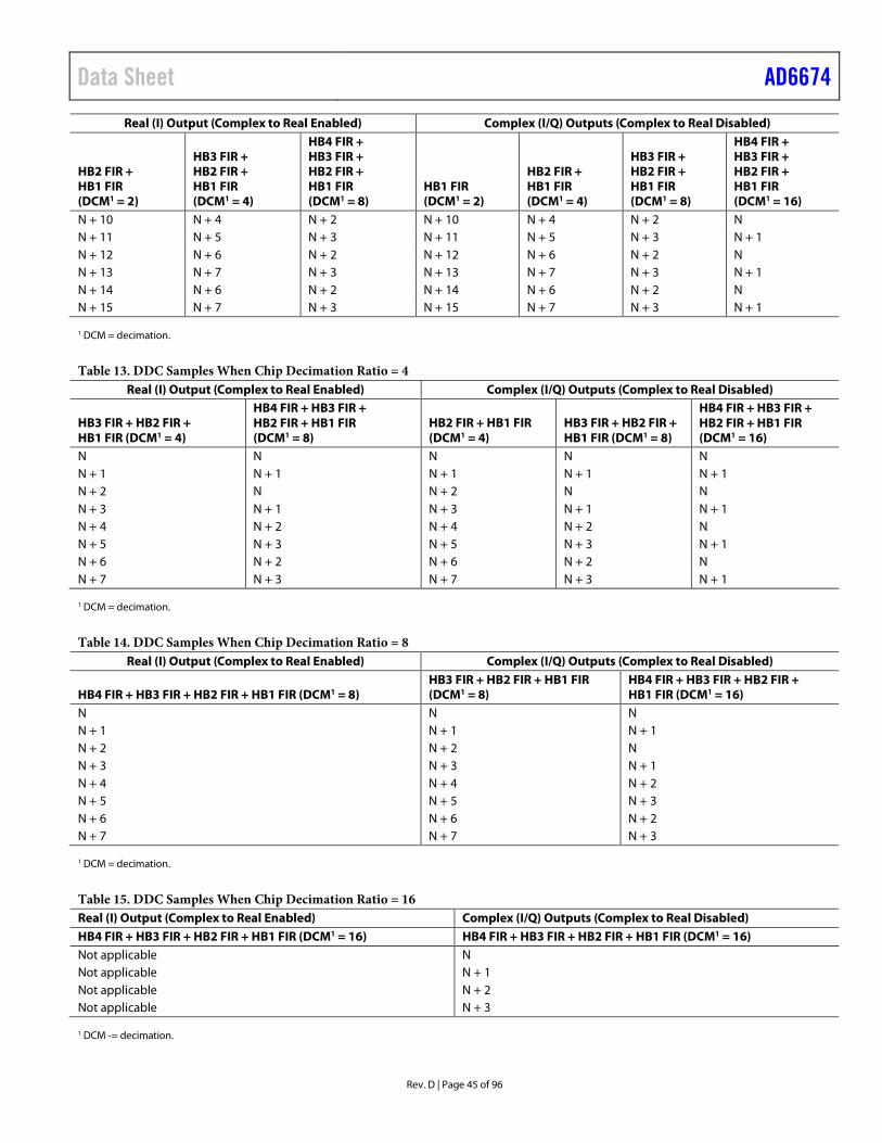
Data Sheet AD6674
Rev. D | Page 45 of 96
Real (I) Output (Complex to Real Enabled) Complex (I/Q) Outputs (Complex to Real Disabled)
HB2 FIR + HB1 FIR (DCM1 = 2)
HB3 FIR + HB2 FIR + HB1 FIR (DCM1 = 4)
HB4 FIR + HB3 FIR + HB2 FIR + HB1 FIR (DCM1 = 8)
HB1 FIR (DCM1 = 2)
HB2 FIR + HB1 FIR (DCM1 = 4)
HB3 FIR + HB2 FIR + HB1 FIR (DCM1 = 8)
HB4 FIR + HB3 FIR + HB2 FIR + HB1 FIR (DCM1 = 16)
N + 10 N + 4 N + 2 N + 10 N + 4 N + 2 N N + 11 N + 5 N + 3 N + 11 N + 5 N + 3 N + 1 N + 12 N + 6 N + 2 N + 12 N + 6 N + 2 N N + 13 N + 7 N + 3 N + 13 N + 7 N + 3 N + 1 N + 14 N + 6 N + 2 N + 14 N + 6 N + 2 N N + 15 N + 7 N + 3 N + 15 N + 7 N + 3 N + 1 1 DCM = decimation.
Table 13. DDC Samples When Chip Decimation Ratio = 4 Real (I) Output (Complex to Real Enabled) Complex (I/Q) Outputs (Complex to Real Disabled)
HB3 FIR + HB2 FIR + HB1 FIR (DCM1 = 4)
HB4 FIR + HB3 FIR + HB2 FIR + HB1 FIR (DCM1 = 8)
HB2 FIR + HB1 FIR (DCM1 = 4)
HB3 FIR + HB2 FIR + HB1 FIR (DCM1 = 8)
HB4 FIR + HB3 FIR + HB2 FIR + HB1 FIR (DCM1 = 16)
N N N N N N + 1 N + 1 N + 1 N + 1 N + 1 N + 2 N N + 2 N N N + 3 N + 1 N + 3 N + 1 N + 1 N + 4 N + 2 N + 4 N + 2 N N + 5 N + 3 N + 5 N + 3 N + 1 N + 6 N + 2 N + 6 N + 2 N N + 7 N + 3 N + 7 N + 3 N + 1 1 DCM = decimation.
Table 14. DDC Samples When Chip Decimation Ratio = 8 Real (I) Output (Complex to Real Enabled) Complex (I/Q) Outputs (Complex to Real Disabled)
HB4 FIR + HB3 FIR + HB2 FIR + HB1 FIR (DCM1 = 8) HB3 FIR + HB2 FIR + HB1 FIR (DCM1 = 8)
HB4 FIR + HB3 FIR + HB2 FIR + HB1 FIR (DCM1 = 16)
N N N N + 1 N + 1 N + 1 N + 2 N + 2 N N + 3 N + 3 N + 1 N + 4 N + 4 N + 2 N + 5 N + 5 N + 3 N + 6 N + 6 N + 2 N + 7 N + 7 N + 3 1 DCM = decimation.
Table 15. DDC Samples When Chip Decimation Ratio = 16 Real (I) Output (Complex to Real Enabled) Complex (I/Q) Outputs (Complex to Real Disabled) HB4 FIR + HB3 FIR + HB2 FIR + HB1 FIR (DCM1 = 16) HB4 FIR + HB3 FIR + HB2 FIR + HB1 FIR (DCM1 = 16) Not applicable N Not applicable N + 1 Not applicable N + 2 Not applicable N + 3 1 DCM -= decimation.
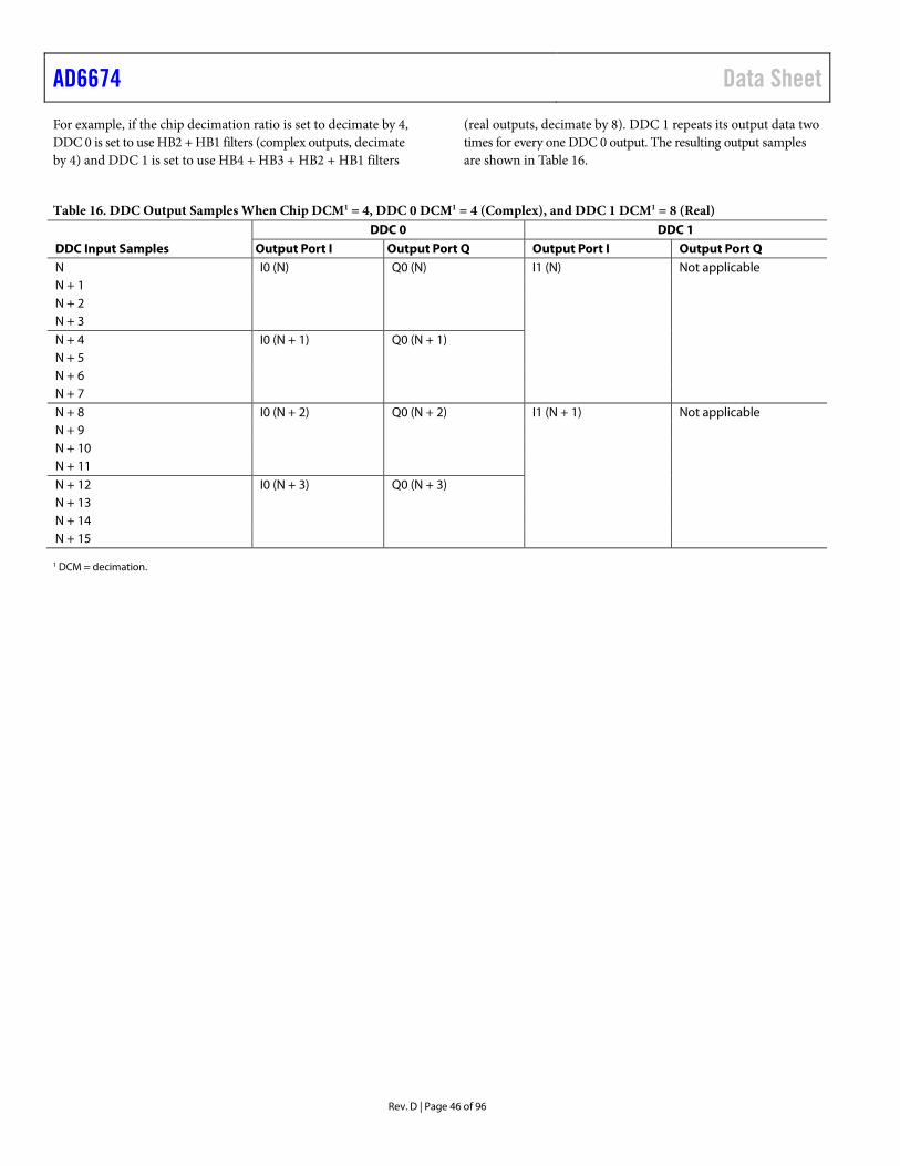
AD6674 Data Sheet
Rev. D | Page 46 of 96
For example, if the chip decimation ratio is set to decimate by 4, DDC 0 is set to use HB2 + HB1 filters (complex outputs, decimate by 4) and DDC 1 is set to use HB4 + HB3 + HB2 + HB1 filters
(real outputs, decimate by 8). DDC 1 repeats its output data two times for every one DDC 0 output. The resulting output samples are shown in Table 16.
Table 16. DDC Output Samples When Chip DCM1 = 4, DDC 0 DCM1 = 4 (Complex), and DDC 1 DCM1 = 8 (Real)
DDC 0 DDC 1
DDC Input Samples Output Port I Output Port Q Output Port I Output Port Q N I0 (N) Q0 (N) I1 (N) Not applicable N + 1 N + 2 N + 3 N + 4 I0 (N + 1) Q0 (N + 1) N + 5 N + 6 N + 7 N + 8 I0 (N + 2) Q0 (N + 2) I1 (N + 1) Not applicable N + 9 N + 10 N + 11 N + 12 I0 (N + 3) Q0 (N + 3) N + 13 N + 14 N + 15 1 DCM = decimation.
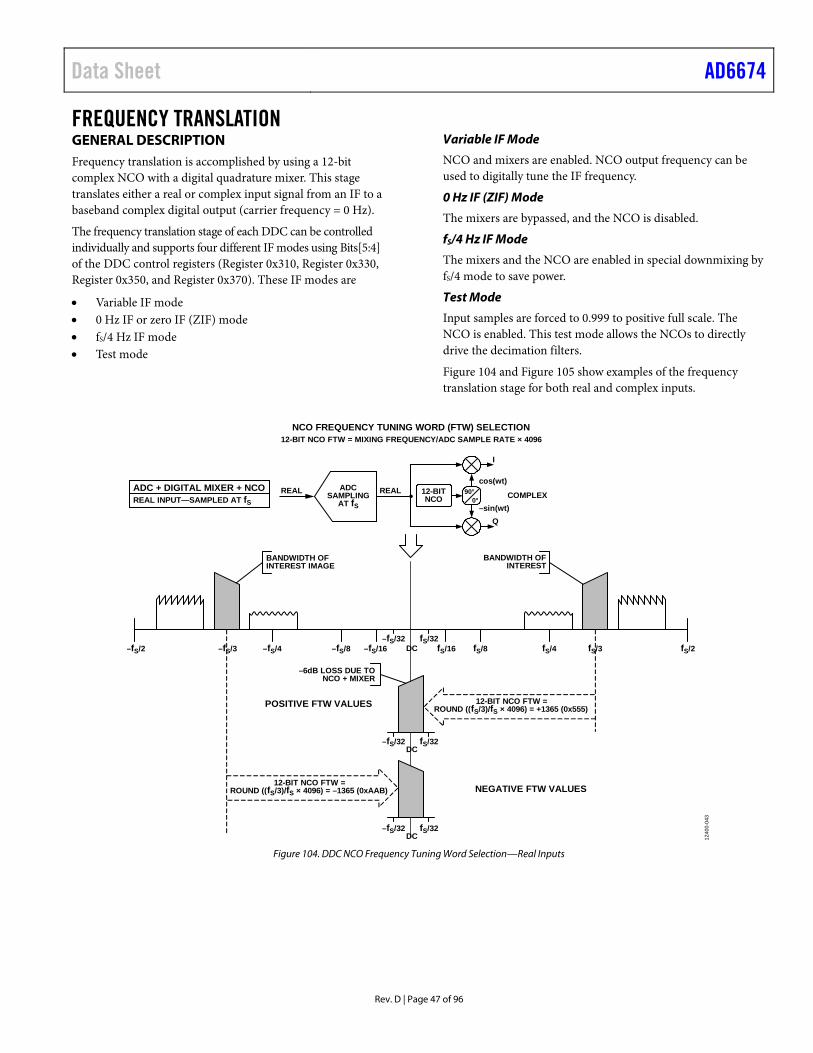
Data Sheet AD6674
Rev. D | Page 47 of 96
FREQUENCY TRANSLATION GENERAL DESCRIPTION Frequency translation is accomplished by using a 12-bit complex NCO with a digital quadrature mixer. This stage translates either a real or complex input signal from an IF to a baseband complex digital output (carrier frequency = 0 Hz).
The frequency translation stage of each DDC can be controlled individually and supports four different IF modes using Bits[5:4] of the DDC control registers (Register 0x310, Register 0x330, Register 0x350, and Register 0x370). These IF modes are
• Variable IF mode • 0 Hz IF or zero IF (ZIF) mode • fS/4 Hz IF mode • Test mode
Variable IF Mode
NCO and mixers are enabled. NCO output frequency can be used to digitally tune the IF frequency.
0 Hz IF (ZIF) Mode
The mixers are bypassed, and the NCO is disabled.
fS/4 Hz IF Mode
The mixers and the NCO are enabled in special downmixing by fS/4 mode to save power.
Test Mode
Input samples are forced to 0.999 to positive full scale. The NCO is enabled. This test mode allows the NCOs to directly drive the decimation filters.
Figure 104 and Figure 105 show examples of the frequency translation stage for both real and complex inputs.
BANDWIDTH OFINTEREST
BANDWIDTH OFINTEREST IMAGE
NCO FREQUENCY TUNING WORD (FTW) SELECTION12-BIT NCO FTW = MIXING FREQUENCY/ADC SAMPLE RATE × 4096
ADC + DIGITAL MIXER + NCOREAL INPUT—SAMPLED AT fS
DC–fS/2 –fS/3 –fS/4 –fS/8 fS/16 fS/8 fS/4 fS/3 fS/2–fS/16–fS/32 fS/32
DC–fS/32 fS/32
DC–fS/32 fS/32
cos(wt)
0°90°
I
Q
ADCSAMPLING
AT fS
REAL REAL
–sin(wt)
12-BITNCO
POSITIVE FTW VALUES
NEGATIVE FTW VALUES
COMPLEX
–6dB LOSS DUE TONCO + MIXER
12-BIT NCO FTW =ROUND ((fS/3)/fS × 4096) = +1365 (0x555)
12-BIT NCO FTW =ROUND ((fS/3)/fS × 4096) = –1365 (0xAAB)
1240
0-04
3
Figure 104. DDC NCO Frequency Tuning Word Selection—Real Inputs
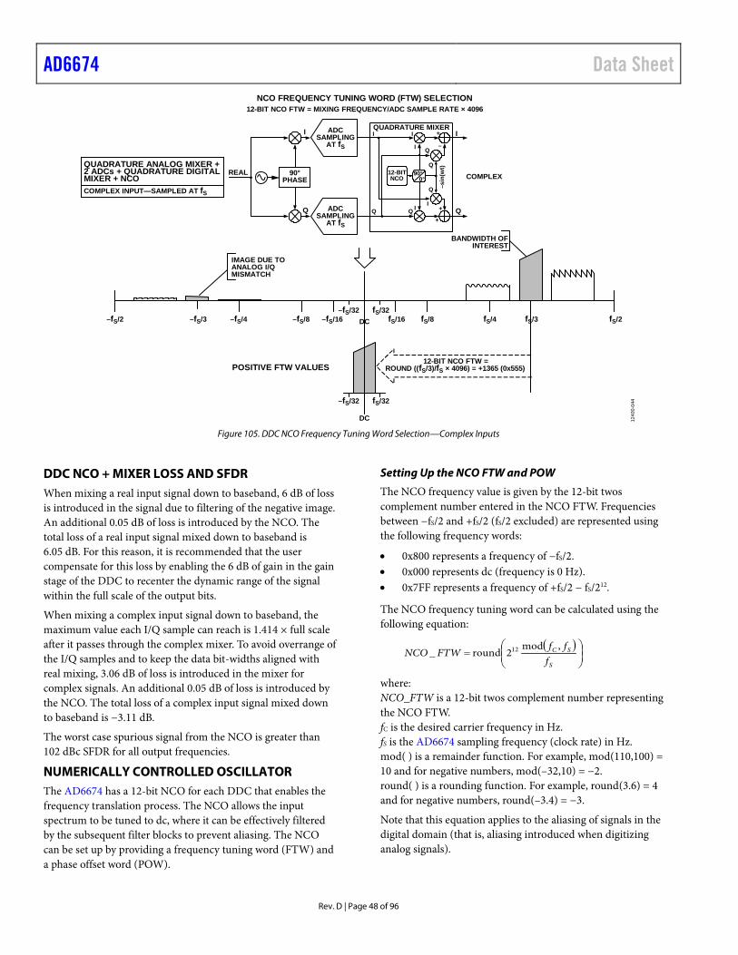
AD6674 Data Sheet
Rev. D | Page 48 of 96
NCO FREQUENCY TUNING WORD (FTW) SELECTION12-BIT NCO FTW = MIXING FREQUENCY/ADC SAMPLE RATE × 4096
QUADRATURE ANALOG MIXER +2 ADCs + QUADRATURE DIGITALMIXER + NCOCOMPLEX INPUT—SAMPLED AT fS
–fS/2 –fS/3 –fS/4 –fS/8 fS/16 fS/8 fS/4 fS/3 fS/2–fS/16–fS/32 fS/32
–fS/32 fS/32
DC
DC
12-BIT NCO FTW =ROUND ((fS/3)/fS × 4096) = +1365 (0x555)
BANDWIDTH OFINTEREST
POSITIVE FTW VALUES
IMAGE DUE TOANALOG I/QMISMATCH
REAL
I
Q
QUADRATURE MIXERI
Q
I
–
+
Q
QI
Q +
+
Q
II
COMPLEX
I
Q
–sin
(wt)
ADCSAMPLING
AT fS
ADCSAMPLING
AT fS
90°PHASE
12-BITNCO
90°0°
1240
0-04
4
Figure 105. DDC NCO Frequency Tuning Word Selection—Complex Inputs
DDC NCO + MIXER LOSS AND SFDR When mixing a real input signal down to baseband, 6 dB of loss is introduced in the signal due to filtering of the negative image. An additional 0.05 dB of loss is introduced by the NCO. The total loss of a real input signal mixed down to baseband is 6.05 dB. For this reason, it is recommended that the user compensate for this loss by enabling the 6 dB of gain in the gain stage of the DDC to recenter the dynamic range of the signal within the full scale of the output bits.
When mixing a complex input signal down to baseband, the maximum value each I/Q sample can reach is 1.414 × full scale after it passes through the complex mixer. To avoid overrange of the I/Q samples and to keep the data bit-widths aligned with real mixing, 3.06 dB of loss is introduced in the mixer for complex signals. An additional 0.05 dB of loss is introduced by the NCO. The total loss of a complex input signal mixed down to baseband is −3.11 dB.
The worst case spurious signal from the NCO is greater than 102 dBc SFDR for all output frequencies.
NUMERICALLY CONTROLLED OSCILLATOR The AD6674 has a 12-bit NCO for each DDC that enables the frequency translation process. The NCO allows the input spectrum to be tuned to dc, where it can be effectively filtered by the subsequent filter blocks to prevent aliasing. The NCO can be set up by providing a frequency tuning word (FTW) and a phase offset word (POW).
Setting Up the NCO FTW and POW
The NCO frequency value is given by the 12-bit twos complement number entered in the NCO FTW. Frequencies between −fS/2 and +fS/2 (fS/2 excluded) are represented using the following frequency words:
• 0x800 represents a frequency of −fS/2. • 0x000 represents dc (frequency is 0 Hz). • 0x7FF represents a frequency of +fS/2 − fS/212.
The NCO frequency tuning word can be calculated using the following equation:
( )
=
S
SC
fff
FTWNCO,mod
2round_ 12
where: NCO_FTW is a 12-bit twos complement number representing the NCO FTW. fC is the desired carrier frequency in Hz. fS is the AD6674 sampling frequency (clock rate) in Hz. mod( ) is a remainder function. For example, mod(110,100) = 10 and for negative numbers, mod(–32,10) = −2. round( ) is a rounding function. For example, round(3.6) = 4 and for negative numbers, round(–3.4) = −3.
Note that this equation applies to the aliasing of signals in the digital domain (that is, aliasing introduced when digitizing analog signals).
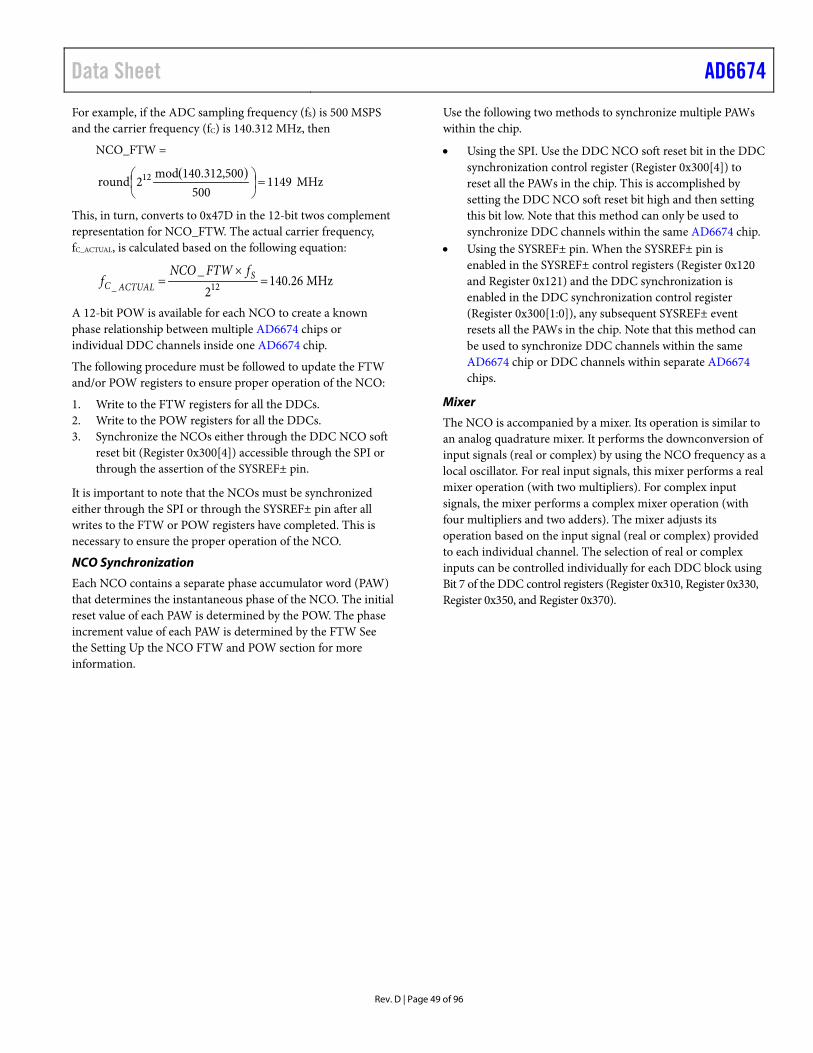
Data Sheet AD6674
Rev. D | Page 49 of 96
For example, if the ADC sampling frequency (fS) is 500 MSPS and the carrier frequency (fC) is 140.312 MHz, then
NCO_FTW =
( )MHz1149
500500,312.140mod
2round 12 =
This, in turn, converts to 0x47D in the 12-bit twos complement representation for NCO_FTW. The actual carrier frequency, fC_ACTUAL, is calculated based on the following equation:
MHz26.1402
_12_ =
×= S
ACTUALCfFTWNCO
f
A 12-bit POW is available for each NCO to create a known phase relationship between multiple AD6674 chips or individual DDC channels inside one AD6674 chip.
The following procedure must be followed to update the FTW and/or POW registers to ensure proper operation of the NCO:
1. Write to the FTW registers for all the DDCs. 2. Write to the POW registers for all the DDCs. 3. Synchronize the NCOs either through the DDC NCO soft
reset bit (Register 0x300[4]) accessible through the SPI or through the assertion of the SYSREF± pin.
It is important to note that the NCOs must be synchronized either through the SPI or through the SYSREF± pin after all writes to the FTW or POW registers have completed. This is necessary to ensure the proper operation of the NCO.
NCO Synchronization
Each NCO contains a separate phase accumulator word (PAW) that determines the instantaneous phase of the NCO. The initial reset value of each PAW is determined by the POW. The phase increment value of each PAW is determined by the FTW See the Setting Up the NCO FTW and POW section for more information.
Use the following two methods to synchronize multiple PAWs within the chip.
• Using the SPI. Use the DDC NCO soft reset bit in the DDC synchronization control register (Register 0x300[4]) to reset all the PAWs in the chip. This is accomplished by setting the DDC NCO soft reset bit high and then setting this bit low. Note that this method can only be used to synchronize DDC channels within the same AD6674 chip.
• Using the SYSREF± pin. When the SYSREF± pin is enabled in the SYSREF± control registers (Register 0x120 and Register 0x121) and the DDC synchronization is enabled in the DDC synchronization control register (Register 0x300[1:0]), any subsequent SYSREF± event resets all the PAWs in the chip. Note that this method can be used to synchronize DDC channels within the same AD6674 chip or DDC channels within separate AD6674 chips.
Mixer
The NCO is accompanied by a mixer. Its operation is similar to an analog quadrature mixer. It performs the downconversion of input signals (real or complex) by using the NCO frequency as a local oscillator. For real input signals, this mixer performs a real mixer operation (with two multipliers). For complex input signals, the mixer performs a complex mixer operation (with four multipliers and two adders). The mixer adjusts its operation based on the input signal (real or complex) provided to each individual channel. The selection of real or complex inputs can be controlled individually for each DDC block using Bit 7 of the DDC control registers (Register 0x310, Register 0x330, Register 0x350, and Register 0x370).
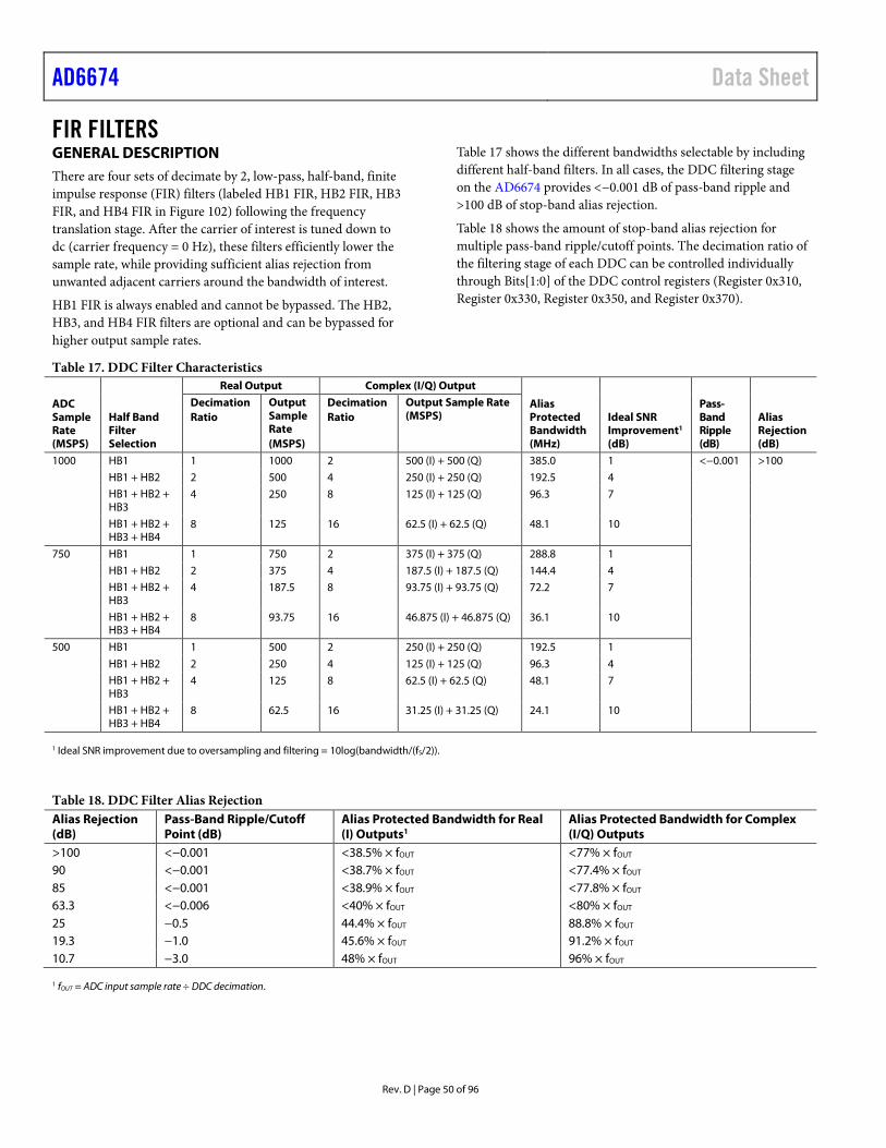
AD6674 Data Sheet
Rev. D | Page 50 of 96
FIR FILTERS GENERAL DESCRIPTION There are four sets of decimate by 2, low-pass, half-band, finite impulse response (FIR) filters (labeled HB1 FIR, HB2 FIR, HB3 FIR, and HB4 FIR in Figure 102) following the frequency translation stage. After the carrier of interest is tuned down to dc (carrier frequency = 0 Hz), these filters efficiently lower the sample rate, while providing sufficient alias rejection from unwanted adjacent carriers around the bandwidth of interest.
HB1 FIR is always enabled and cannot be bypassed. The HB2, HB3, and HB4 FIR filters are optional and can be bypassed for higher output sample rates.
Table 17 shows the different bandwidths selectable by including different half-band filters. In all cases, the DDC filtering stage on the AD6674 provides <−0.001 dB of pass-band ripple and >100 dB of stop-band alias rejection.
Table 18 shows the amount of stop-band alias rejection for multiple pass-band ripple/cutoff points. The decimation ratio of the filtering stage of each DDC can be controlled individually through Bits[1:0] of the DDC control registers (Register 0x310, Register 0x330, Register 0x350, and Register 0x370).
Table 17. DDC Filter Characteristics
ADC Sample Rate (MSPS)
Half Band Filter Selection
Real Output Complex (I/Q) Output
Alias Protected Bandwidth (MHz)
Ideal SNR Improvement1 (dB)
Pass-Band Ripple (dB)
Alias Rejection (dB)
Decimation Ratio
Output Sample Rate (MSPS)
Decimation Ratio
Output Sample Rate (MSPS)
1000 HB1 1 1000 2 500 (I) + 500 (Q) 385.0 1 <−0.001 >100
HB1 + HB2 2 500 4 250 (I) + 250 (Q) 192.5 4
HB1 + HB2 + HB3
4 250 8 125 (I) + 125 (Q) 96.3 7
HB1 + HB2 + HB3 + HB4
8 125 16 62.5 (I) + 62.5 (Q) 48.1 10
750 HB1 1 750 2 375 (I) + 375 (Q) 288.8 1
HB1 + HB2 2 375 4 187.5 (I) + 187.5 (Q) 144.4 4
HB1 + HB2 + HB3
4 187.5 8 93.75 (I) + 93.75 (Q) 72.2 7
HB1 + HB2 + HB3 + HB4
8 93.75 16 46.875 (I) + 46.875 (Q) 36.1 10
500 HB1 1 500 2 250 (I) + 250 (Q) 192.5 1
HB1 + HB2 2 250 4 125 (I) + 125 (Q) 96.3 4
HB1 + HB2 + HB3
4 125 8 62.5 (I) + 62.5 (Q) 48.1 7
HB1 + HB2 + HB3 + HB4
8 62.5 16 31.25 (I) + 31.25 (Q) 24.1 10
1 Ideal SNR improvement due to oversampling and filtering = 10log(bandwidth/(fS/2)).
Table 18. DDC Filter Alias Rejection Alias Rejection (dB)
Pass-Band Ripple/Cutoff Point (dB)
Alias Protected Bandwidth for Real (I) Outputs1
Alias Protected Bandwidth for Complex (I/Q) Outputs
>100 <−0.001 <38.5% × fOUT <77% × fOUT 90 <−0.001 <38.7% × fOUT <77.4% × fOUT 85 <−0.001 <38.9% × fOUT <77.8% × fOUT 63.3 <−0.006 <40% × fOUT <80% × fOUT 25 −0.5 44.4% × fOUT 88.8% × fOUT 19.3 −1.0 45.6% × fOUT 91.2% × fOUT 10.7 −3.0 48% × fOUT 96% × fOUT 1 fOUT = ADC input sample rate ÷ DDC decimation.
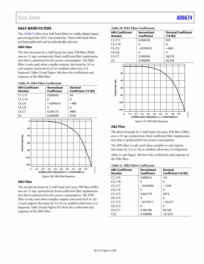
Data Sheet AD6674
Rev. D | Page 51 of 96
HALF-BAND FILTERS The AD6674 offers four half-band filters to enable digital signal processing of the ADC converted data. These half-band filters are bypassable and can be individually selected.
HB4 Filter
The first decimate by 2, half-band, low-pass, FIR filter (HB4) uses an 11-tap, symmetrical, fixed coefficient filter implementa-tion that is optimized for low power consumption. The HB4 filter is only used when complex outputs (decimate by 16) or real outputs (decimate by 8) are enabled; otherwise, it is bypassed. Table 19 and Figure 106 show the coefficients and response of the HB4 filter.
Table 19. HB4 Filter Coefficients HB4 Coefficient Number
Normalized Coefficient
Decimal Coefficient (15-Bit)
C1, C11 0.006042 99 C2, C10 0 0 C3, C9 −0.049316 −808 C4, C8 0 0 C5, C7 0.293273 4805 C6 0.500000 8192
0
–120
–100
–80
–60
–40
–20
0 0.1 0.2 0.3 0.4 0.5 0.6 0.7 0.8 0.9
MAG
NITU
DE (d
B)
NORMALIZED FREQUENCY (× π RAD/SAMPLE) 1240
0-04
5
Figure 106. HB4 Filter Response
HB3 Filter
The second decimate by 2, half-band, low-pass, FIR filter (HB3) uses an 11-tap, symmetrical, fixed coefficient filter implementa-tion that is optimized for low power consumption. The HB3 filter is only used when complex outputs (decimate by 8 or 16) or real outputs (decimate by 4 or 8) are enabled; otherwise, it is bypassed. Table 20 and Figure 107 show the coefficients and response of the HB3 filter.
Table 20. HB3 Filter Coefficients HB3 Coefficient Number
Normalized Coefficient
Decimal Coefficient (18-Bit)
C1, C11 0.006554 859 C2, C10 0 0 C3, C9 −0.050819 −6661 C4, C8 0 0 C5, C7 0.294266 38,570 C6 0.500000 65,536
0
–120
–100
–80
–60
–40
–20
0 0.1 0.2 0.3 0.4 0.5 0.6 0.7 0.8 0.9M
AGNI
TUDE
(dB)
NORMALIZED FREQUENCY (× π RAD/SAMPLE) 1240
0-04
6
Figure 107. HB3 Filter Response
HB2 Filter
The third decimate by 2, half-band, low-pass, FIR filter (HB2) uses a 19-tap, symmetrical, fixed coefficient filter implementa-tion that is optimized for low power consumption.
The HB2 filter is only used when complex or real outputs (decimate by 4, 8, or 16) is enabled; otherwise, it is bypassed.
Table 21 and Figure 108 show the coefficients and response of the HB2 filter.
Table 21. HB2 Filter Coefficients HB2 Coefficient Number
Normalized Coefficient
Decimal Coefficient (19-Bit)
C1, C19 0.000614 161 C2, C18 0 0 C3, C17 −0.005066 −1328 C4, C16 0 0 C5, C15 0.022179 5814 C6, C14 0 0 C7, C13 −0.073517 −19,272 C8, C12 0 0 C9, C11 0.305786 80,160 C10 0.500000 131,072
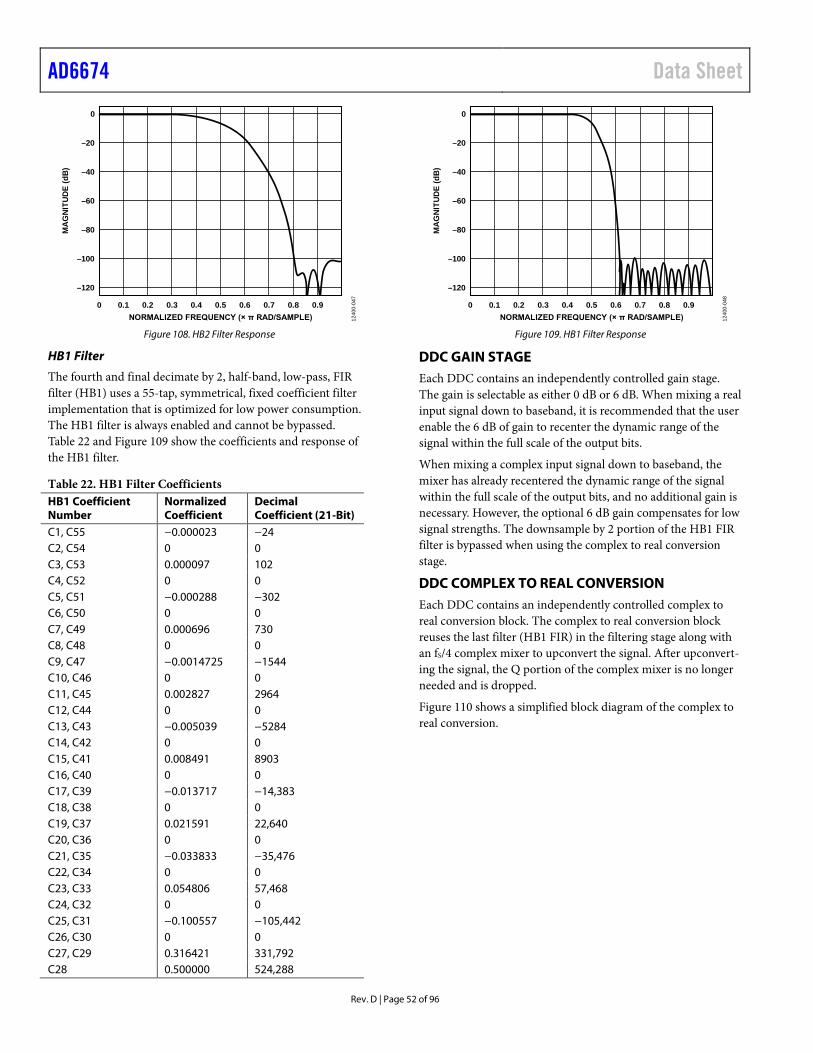
AD6674 Data Sheet
Rev. D | Page 52 of 96
0
–120
–100
–80
–60
–40
–20
0 0.1 0.2 0.3 0.4 0.5 0.6 0.7 0.8 0.9
MAG
NITU
DE (d
B)
NORMALIZED FREQUENCY (× π RAD/SAMPLE) 1240
0-04
7
Figure 108. HB2 Filter Response
HB1 Filter
The fourth and final decimate by 2, half-band, low-pass, FIR filter (HB1) uses a 55-tap, symmetrical, fixed coefficient filter implementation that is optimized for low power consumption. The HB1 filter is always enabled and cannot be bypassed. Table 22 and Figure 109 show the coefficients and response of the HB1 filter.
Table 22. HB1 Filter Coefficients HB1 Coefficient Number
Normalized Coefficient
Decimal Coefficient (21-Bit)
C1, C55 −0.000023 −24 C2, C54 0 0 C3, C53 0.000097 102 C4, C52 0 0 C5, C51 −0.000288 −302 C6, C50 0 0 C7, C49 0.000696 730 C8, C48 0 0 C9, C47 −0.0014725 −1544 C10, C46 0 0 C11, C45 0.002827 2964 C12, C44 0 0 C13, C43 −0.005039 −5284 C14, C42 0 0 C15, C41 0.008491 8903 C16, C40 0 0 C17, C39 −0.013717 −14,383 C18, C38 0 0 C19, C37 0.021591 22,640 C20, C36 0 0 C21, C35 −0.033833 −35,476 C22, C34 0 0 C23, C33 0.054806 57,468 C24, C32 0 0 C25, C31 −0.100557 −105,442 C26, C30 0 0 C27, C29 0.316421 331,792 C28 0.500000 524,288
0
–120
–100
–80
–60
–40
–20
0 0.1 0.2 0.3 0.4 0.5 0.6 0.7 0.8 0.9
MAG
NITU
DE (d
B)
NORMALIZED FREQUENCY (× π RAD/SAMPLE) 1240
0-04
8
Figure 109. HB1 Filter Response
DDC GAIN STAGE Each DDC contains an independently controlled gain stage. The gain is selectable as either 0 dB or 6 dB. When mixing a real input signal down to baseband, it is recommended that the user enable the 6 dB of gain to recenter the dynamic range of the signal within the full scale of the output bits.
When mixing a complex input signal down to baseband, the mixer has already recentered the dynamic range of the signal within the full scale of the output bits, and no additional gain is necessary. However, the optional 6 dB gain compensates for low signal strengths. The downsample by 2 portion of the HB1 FIR filter is bypassed when using the complex to real conversion stage.
DDC COMPLEX TO REAL CONVERSION Each DDC contains an independently controlled complex to real conversion block. The complex to real conversion block reuses the last filter (HB1 FIR) in the filtering stage along with an fS/4 complex mixer to upconvert the signal. After upconvert-ing the signal, the Q portion of the complex mixer is no longer needed and is dropped.
Figure 110 shows a simplified block diagram of the complex to real conversion.
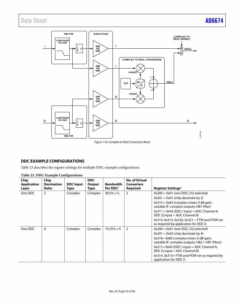
Data Sheet AD6674
Rev. D | Page 53 of 96
LOW-PASSFILTER
2I
Q
REAL
HB1 FIR
LOW-PASSFILTER
2
HB1 FIR
0
1
COMPLEX TOREAL ENABLE
Q
90°0°
+
–
COMPLEX TO REAL CONVERSION
I
Q
I
Q
GAIN STAGE
cos(wt)
sin(wt)
fS/4
I/REAL
0dBOR6dB
0dBOR6dB
0dBOR6dB
0dBOR6dB
1240
0-04
9
Figure 110. Complex to Real Conversion Block
DDC EXAMPLE CONFIGURATIONS Table 23 describes the register settings for multiple DDC example configurations.
Table 23. DDC Example Configurations Chip Application Layer
Chip Decimation Ratio
DDC Input Type
DDC Output Type
Bandwidth Per DDC1
No. of Virtual Converters Required Register Settings2
One DDC 2 Complex Complex 38.5% × fS 2 0x200 = 0x01 (one DDC; I/Q selected) 0x201 = 0x01 (chip decimate by 2) 0x310 = 0x83 (complex mixer; 0 dB gain;
variable IF; complex outputs; HB1 filter) 0x311 = 0x04 (DDC I input = ADC Channel A;
DDC Q input = ADC Channel B) 0x314, 0x315, 0x320, 0x321 = FTW and POW set
as required by application for DDC 0 One DDC 4 Complex Complex 19.25% × fS 2 0x200 = 0x01 (one DDC; I/Q selected) 0x201 = 0x02 (chip decimate by 4) 0x310= 0x80 (complex mixer; 0 dB gain;
variable IF; complex outputs; HB2 + HB1 filters) 0x311= 0x04 (DDC I input = ADC Channel A;
DDC Q input = ADC Channel B) 0x314, 0x315= FTW and POW set as required by
application for DDC 0
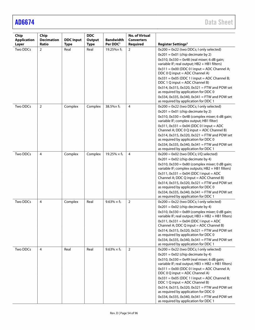
AD6674 Data Sheet
Rev. D | Page 54 of 96
Chip Application Layer
Chip Decimation Ratio
DDC Input Type
DDC Output Type
Bandwidth Per DDC1
No. of Virtual Converters Required Register Settings2
Two DDCs 2 Real Real 19.25%× fS 2 0x200 = 0x22 (two DDCs; I only selected) 0x201 = 0x01 (chip decimate by 2) 0x310, 0x330 = 0x48 (real mixer; 6 dB gain;
variable IF; real output; HB2 + HB1 filters) 0x311 = 0x00 (DDC 0 I input = ADC Channel A;
DDC 0 Q input = ADC Channel A) 0x331 = 0x05 (DDC 1 I input = ADC Channel B;
DDC 1 Q input = ADC Channel B) 0x314, 0x315, 0x320, 0x321 = FTW and POW set
as required by application for DDC 0 0x334, 0x335, 0x340, 0x341 = FTW and POW set
as required by application for DDC 1 Two DDCs 2 Complex Complex 38.5%× fS 4 0x200 = 0x22 (two DDCs; I only selected) 0x201 = 0x01 (chip decimate by 2) 0x310, 0x330 = 0x4B (complex mixer; 6 dB gain;
variable IF; complex output; HB1 filter) 0x311, 0x331 = 0x04 (DDC 0 I input = ADC
Channel A; DDC 0 Q input = ADC Channel B) 0x314, 0x315, 0x320, 0x321 = FTW and POW set
as required by application for DDC 0 0x334, 0x335, 0x340, 0x341 = FTW and POW set
as required by application for DDC 1 Two DDCs 4 Complex Complex 19.25% × fS 4 0x200 = 0x02 (two DDCs; I/Q selected) 0x201 = 0x02 (chip decimate by 4) 0x310, 0x330 = 0x80 (complex mixer; 0 dB gain;
variable IF; complex outputs; HB2 + HB1 filters) 0x311, 0x331 = 0x04 (DDC I input = ADC
Channel A; DDC Q input = ADC Channel B) 0x314, 0x315, 0x320, 0x321 = FTW and POW set
as required by application for DDC 0 0x334, 0x335, 0x340, 0x341 = FTW and POW set
as required by application for DDC 1 Two DDCs 4 Complex Real 9.63% × fS 2 0x200 = 0x22 (two DDCs; I only selected) 0x201 = 0x02 (chip decimate by 4) 0x310, 0x330 = 0x89 (complex mixer; 0 dB gain;
variable IF; real output; HB3 + HB2 + HB1 filters) 0x311, 0x331 = 0x04 (DDC I input = ADC
Channel A; DDC Q input = ADC Channel B) 0x314, 0x315, 0x320, 0x321 = FTW and POW set
as required by application for DDC 0 0x334, 0x335, 0x340, 0x341 = FTW and POW set
as required by application for DDC 1 Two DDCs 4 Real Real 9.63% × fS 2 0x200 = 0x22 (two DDCs; I only selected) 0x201 = 0x02 (chip decimate by 4) 0x310, 0x330 = 0x49 (real mixer; 6 dB gain;
variable IF; real output; HB3 + HB2 + HB1 filters) 0x311 = 0x00 (DDC 0 I input = ADC Channel A;
DDC 0 Q input = ADC Channel A) 0x331 = 0x05 (DDC 1 I input = ADC Channel B;
DDC 1 Q input = ADC Channel B) 0x314, 0x315, 0x320, 0x321 = FTW and POW set
as required by application for DDC 0 0x334, 0x335, 0x340, 0x341 = FTW and POW set
as required by application for DDC 1
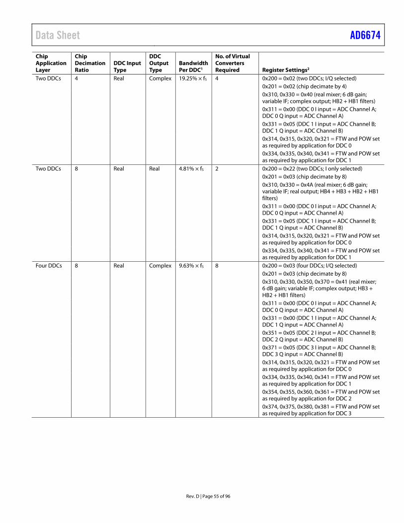
Data Sheet AD6674
Rev. D | Page 55 of 96
Chip Application Layer
Chip Decimation Ratio
DDC Input Type
DDC Output Type
Bandwidth Per DDC1
No. of Virtual Converters Required Register Settings2
Two DDCs 4 Real Complex 19.25% × fS 4 0x200 = 0x02 (two DDCs; I/Q selected) 0x201 = 0x02 (chip decimate by 4) 0x310, 0x330 = 0x40 (real mixer; 6 dB gain;
variable IF; complex output; HB2 + HB1 filters) 0x311 = 0x00 (DDC 0 I input = ADC Channel A;
DDC 0 Q input = ADC Channel A) 0x331 = 0x05 (DDC 1 I input = ADC Channel B;
DDC 1 Q input = ADC Channel B) 0x314, 0x315, 0x320, 0x321 = FTW and POW set
as required by application for DDC 0 0x334, 0x335, 0x340, 0x341 = FTW and POW set
as required by application for DDC 1 Two DDCs 8 Real Real 4.81% × fS 2 0x200 = 0x22 (two DDCs; I only selected) 0x201 = 0x03 (chip decimate by 8) 0x310, 0x330 = 0x4A (real mixer; 6 dB gain;
variable IF; real output; HB4 + HB3 + HB2 + HB1 filters)
0x311 = 0x00 (DDC 0 I input = ADC Channel A; DDC 0 Q input = ADC Channel A)
0x331 = 0x05 (DDC 1 I input = ADC Channel B; DDC 1 Q input = ADC Channel B)
0x314, 0x315, 0x320, 0x321 = FTW and POW set as required by application for DDC 0
0x334, 0x335, 0x340, 0x341 = FTW and POW set as required by application for DDC 1
Four DDCs 8 Real Complex 9.63% × fS 8 0x200 = 0x03 (four DDCs; I/Q selected) 0x201 = 0x03 (chip decimate by 8) 0x310, 0x330, 0x350, 0x370 = 0x41 (real mixer;
6 dB gain; variable IF; complex output; HB3 + HB2 + HB1 filters)
0x311 = 0x00 (DDC 0 I input = ADC Channel A; DDC 0 Q input = ADC Channel A)
0x331 = 0x00 (DDC 1 I input = ADC Channel A; DDC 1 Q input = ADC Channel A)
0x351 = 0x05 (DDC 2 I input = ADC Channel B; DDC 2 Q input = ADC Channel B)
0x371 = 0x05 (DDC 3 I input = ADC Channel B; DDC 3 Q input = ADC Channel B)
0x314, 0x315, 0x320, 0x321 = FTW and POW set as required by application for DDC 0
0x334, 0x335, 0x340, 0x341 = FTW and POW set as required by application for DDC 1
0x354, 0x355, 0x360, 0x361 = FTW and POW set as required by application for DDC 2
0x374, 0x375, 0x380, 0x381 = FTW and POW set as required by application for DDC 3
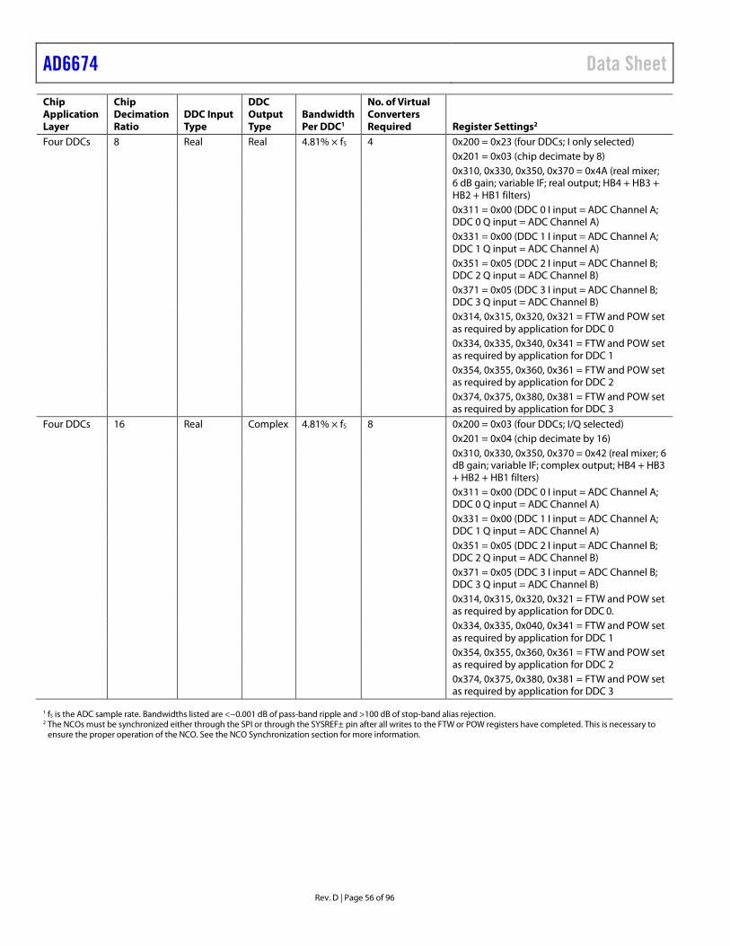
AD6674 Data Sheet
Rev. D | Page 56 of 96
Chip Application Layer
Chip Decimation Ratio
DDC Input Type
DDC Output Type
Bandwidth Per DDC1
No. of Virtual Converters Required Register Settings2
Four DDCs 8 Real Real 4.81% × fS 4 0x200 = 0x23 (four DDCs; I only selected) 0x201 = 0x03 (chip decimate by 8) 0x310, 0x330, 0x350, 0x370 = 0x4A (real mixer;
6 dB gain; variable IF; real output; HB4 + HB3 + HB2 + HB1 filters)
0x311 = 0x00 (DDC 0 I input = ADC Channel A; DDC 0 Q input = ADC Channel A)
0x331 = 0x00 (DDC 1 I input = ADC Channel A; DDC 1 Q input = ADC Channel A)
0x351 = 0x05 (DDC 2 I input = ADC Channel B; DDC 2 Q input = ADC Channel B)
0x371 = 0x05 (DDC 3 I input = ADC Channel B; DDC 3 Q input = ADC Channel B)
0x314, 0x315, 0x320, 0x321 = FTW and POW set as required by application for DDC 0
0x334, 0x335, 0x340, 0x341 = FTW and POW set as required by application for DDC 1
0x354, 0x355, 0x360, 0x361 = FTW and POW set as required by application for DDC 2
0x374, 0x375, 0x380, 0x381 = FTW and POW set as required by application for DDC 3
Four DDCs 16 Real Complex 4.81% × fS 8 0x200 = 0x03 (four DDCs; I/Q selected) 0x201 = 0x04 (chip decimate by 16) 0x310, 0x330, 0x350, 0x370 = 0x42 (real mixer; 6
dB gain; variable IF; complex output; HB4 + HB3 + HB2 + HB1 filters)
0x311 = 0x00 (DDC 0 I input = ADC Channel A; DDC 0 Q input = ADC Channel A)
0x331 = 0x00 (DDC 1 I input = ADC Channel A; DDC 1 Q input = ADC Channel A)
0x351 = 0x05 (DDC 2 I input = ADC Channel B; DDC 2 Q input = ADC Channel B)
0x371 = 0x05 (DDC 3 I input = ADC Channel B; DDC 3 Q input = ADC Channel B)
0x314, 0x315, 0x320, 0x321 = FTW and POW set as required by application for DDC 0.
0x334, 0x335, 0x040, 0x341 = FTW and POW set as required by application for DDC 1
0x354, 0x355, 0x360, 0x361 = FTW and POW set as required by application for DDC 2
0x374, 0x375, 0x380, 0x381 = FTW and POW set as required by application for DDC 3
1 fS is the ADC sample rate. Bandwidths listed are <−0.001 dB of pass-band ripple and >100 dB of stop-band alias rejection. 2 The NCOs must be synchronized either through the SPI or through the SYSREF± pin after all writes to the FTW or POW registers have completed. This is necessary to
ensure the proper operation of the NCO. See the NCO Synchronization section for more information.
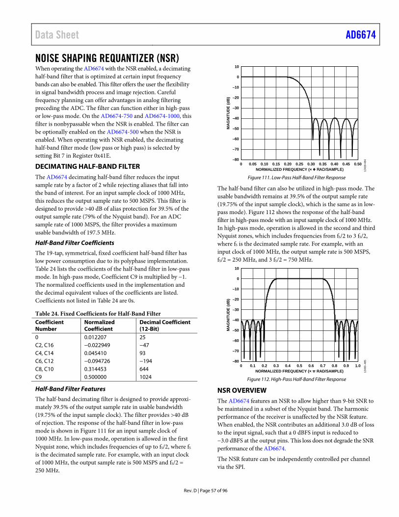
Data Sheet AD6674
Rev. D | Page 57 of 96
NOISE SHAPING REQUANTIZER (NSR) When operating the AD6674 with the NSR enabled, a decimating half-band filter that is optimized at certain input frequency bands can also be enabled. This filter offers the user the flexibility in signal bandwidth process and image rejection. Careful frequency planning can offer advantages in analog filtering preceding the ADC. The filter can function either in high-pass or low-pass mode. On the AD6674-750 and AD6674-1000, this filter is nonbypassable when the NSR is enabled. The filter can be optionally enabled on the AD6674-500 when the NSR is enabled. When operating with NSR enabled, the decimating half-band filter mode (low pass or high pass) is selected by setting Bit 7 in Register 0x41E.
DECIMATING HALF-BAND FILTER The AD6674 decimating half-band filter reduces the input sample rate by a factor of 2 while rejecting aliases that fall into the band of interest. For an input sample clock of 1000 MHz, this reduces the output sample rate to 500 MSPS. This filter is designed to provide >40 dB of alias protection for 39.5% of the output sample rate (79% of the Nyquist band). For an ADC sample rate of 1000 MSPS, the filter provides a maximum usable bandwidth of 197.5 MHz.
Half-Band Filter Coefficients
The 19-tap, symmetrical, fixed coefficient half-band filter has low power consumption due to its polyphase implementation. Table 24 lists the coefficients of the half-band filter in low-pass mode. In high-pass mode, Coefficient C9 is multiplied by −1. The normalized coefficients used in the implementation and the decimal equivalent values of the coefficients are listed. Coefficients not listed in Table 24 are 0s.
Table 24. Fixed Coefficients for Half-Band Filter Coefficient Number
Normalized Coefficient
Decimal Coefficient (12-Bit)
0 0.012207 25 C2, C16 −0.022949 −47 C4, C14 0.045410 93 C6, C12 −0.094726 −194 C8, C10 0.314453 644 C9 0.500000 1024
Half-Band Filter Features
The half-band decimating filter is designed to provide approxi-mately 39.5% of the output sample rate in usable bandwidth (19.75% of the input sample clock). The filter provides >40 dB of rejection. The response of the half-band filter in low-pass mode is shown in Figure 111 for an input sample clock of 1000 MHz. In low-pass mode, operation is allowed in the first Nyquist zone, which includes frequencies of up to fS/2, where fS is the decimated sample rate. For example, with an input clock of 1000 MHz, the output sample rate is 500 MSPS and fS/2 = 250 MHz.
–80
–70
–60
–50
–40
–30
–20
–10
0
10
0 0.05 0.10 0.15 0.20 0.25NORMALIZED FREQUENCY (× RAD/SAMPLE)
MA
GN
ITU
DE
(dB
)
0.30 0.35 0.40 0.45 0.50
1240
0-48
4
Figure 111. Low-Pass Half-Band Filter Response
The half-band filter can also be utilized in high-pass mode. The usable bandwidth remains at 39.5% of the output sample rate (19.75% of the input sample clock), which is the same as in low-pass mode). Figure 112 shows the response of the half-band filter in high-pass mode with an input sample clock of 1000 MHz. In high-pass mode, operation is allowed in the second and third Nyquist zones, which includes frequencies from fS/2 to 3 fS/2, where fS is the decimated sample rate. For example, with an input clock of 1000 MHz, the output sample rate is 500 MSPS, fS/2 = 250 MHz, and 3 fS/2 = 750 MHz.
–80
–70
–60
–50
–40
–30
–20
–10
0
10
0 0.1 0.2 0.3 0.4 0.5NORMALIZED FREQUENCY (× π RAD/SAMPLE)
MA
GN
ITU
DE
(dB
)
0.6 0.7 0.8 0.9 1.0 1
2400
–485
Figure 112. High-Pass Half-Band Filter Response
NSR OVERVIEW The AD6674 features an NSR to allow higher than 9-bit SNR to be maintained in a subset of the Nyquist band. The harmonic performance of the receiver is unaffected by the NSR feature. When enabled, the NSR contributes an additional 3.0 dB of loss to the input signal, such that a 0 dBFS input is reduced to −3.0 dBFS at the output pins. This loss does not degrade the SNR performance of the AD6674.
The NSR feature can be independently controlled per channel via the SPI.
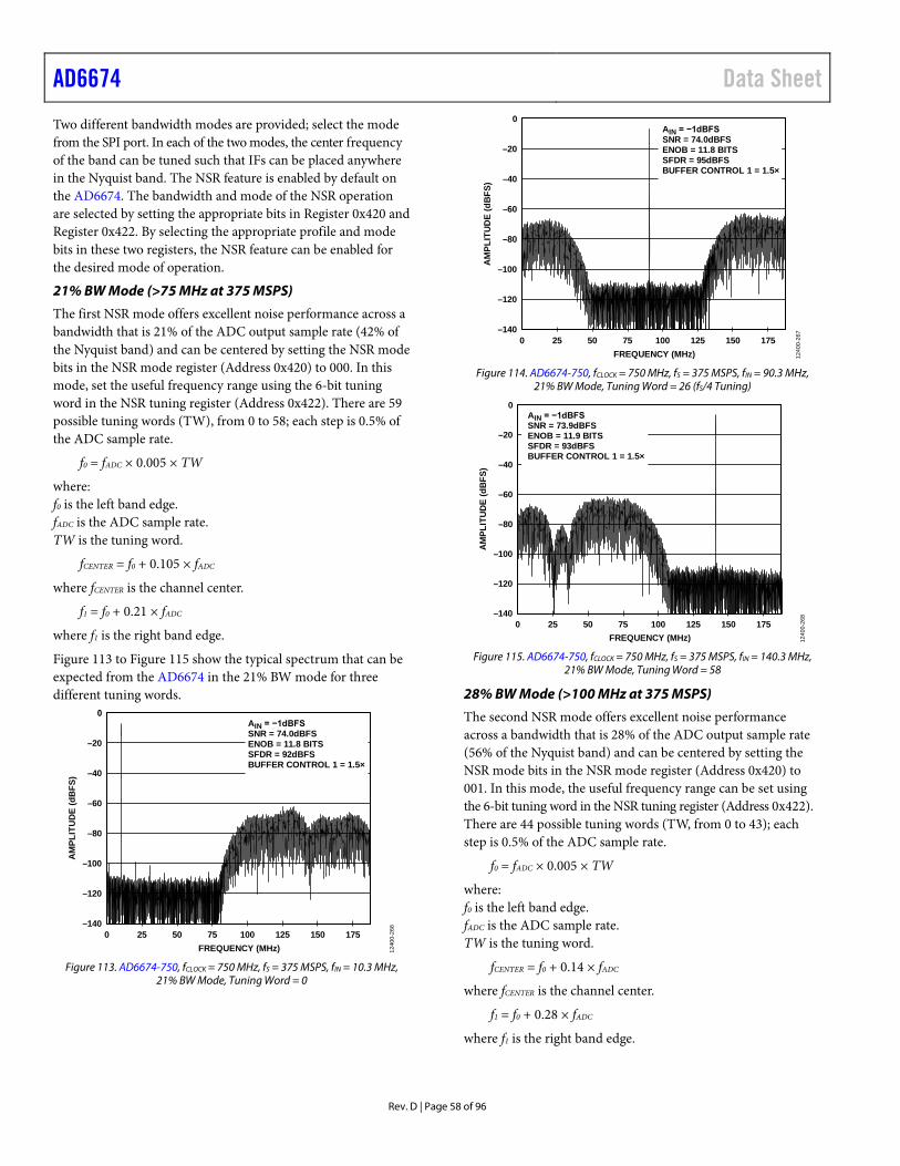
AD6674 Data Sheet
Rev. D | Page 58 of 96
Two different bandwidth modes are provided; select the mode from the SPI port. In each of the two modes, the center frequency of the band can be tuned such that IFs can be placed anywhere in the Nyquist band. The NSR feature is enabled by default on the AD6674. The bandwidth and mode of the NSR operation are selected by setting the appropriate bits in Register 0x420 and Register 0x422. By selecting the appropriate profile and mode bits in these two registers, the NSR feature can be enabled for the desired mode of operation.
21% BW Mode (>75 MHz at 375 MSPS)
The first NSR mode offers excellent noise performance across a bandwidth that is 21% of the ADC output sample rate (42% of the Nyquist band) and can be centered by setting the NSR mode bits in the NSR mode register (Address 0x420) to 000. In this mode, set the useful frequency range using the 6-bit tuning word in the NSR tuning register (Address 0x422). There are 59 possible tuning words (TW), from 0 to 58; each step is 0.5% of the ADC sample rate.
f0 = fADC × 0.005 × TW
where: f0 is the left band edge. fADC is the ADC sample rate. TW is the tuning word.
fCENTER = f0 + 0.105 × fADC
where fCENTER is the channel center.
f1 = f0 + 0.21 × fADC
where f1 is the right band edge.
Figure 113 to Figure 115 show the typical spectrum that can be expected from the AD6674 in the 21% BW mode for three different tuning words.
–140
0
–20
–40
–60
–80
–100
–120
AM
PLIT
UD
E (d
BFS
)
FREQUENCY (MHz)
AIN = −1dBFSSNR = 74.0dBFSENOB = 11.8 BITSSFDR = 92dBFSBUFFER CONTROL 1 = 1.5×
1240
0-26
6
0 175150125100755025
Figure 113. AD6674-750, fCLOCK = 750 MHz, fS = 375 MSPS, fIN = 10.3 MHz, 21% BW Mode, Tuning Word = 0
–140
0
–20
–40
–60
–80
–100
–120
0 175150125100755025
AM
PLIT
UD
E (d
BFS
)
FREQUENCY (MHz)
AIN = −1dBFSSNR = 74.0dBFSENOB = 11.8 BITSSFDR = 95dBFSBUFFER CONTROL 1 = 1.5×
1240
0-26
7
Figure 114. AD6674-750, fCLOCK = 750 MHz, fS = 375 MSPS, fIN = 90.3 MHz, 21% BW Mode, Tuning Word = 26 (fS/4 Tuning)
–140
0
–20
–40
–60
–80
–100
–120
0 175150125100755025
AM
PLIT
UD
E (d
BFS
)
FREQUENCY (MHz)
AIN = −1dBFSSNR = 73.9dBFSENOB = 11.9 BITSSFDR = 93dBFSBUFFER CONTROL 1 = 1.5×
1240
0-26
8
Figure 115. AD6674-750, fCLOCK = 750 MHz, fS = 375 MSPS, fIN = 140.3 MHz, 21% BW Mode, Tuning Word = 58
28% BW Mode (>100 MHz at 375 MSPS)
The second NSR mode offers excellent noise performance across a bandwidth that is 28% of the ADC output sample rate (56% of the Nyquist band) and can be centered by setting the NSR mode bits in the NSR mode register (Address 0x420) to 001. In this mode, the useful frequency range can be set using the 6-bit tuning word in the NSR tuning register (Address 0x422). There are 44 possible tuning words (TW, from 0 to 43); each step is 0.5% of the ADC sample rate.
f0 = fADC × 0.005 × TW
where: f0 is the left band edge. fADC is the ADC sample rate. TW is the tuning word.
fCENTER = f0 + 0.14 × fADC
where fCENTER is the channel center.
f1 = f0 + 0.28 × fADC
where f1 is the right band edge.
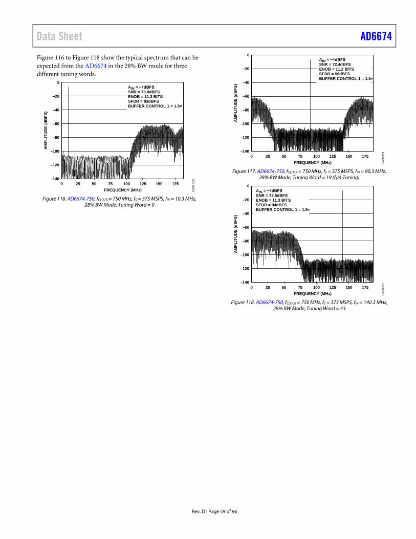
Data Sheet AD6674
Rev. D | Page 59 of 96
Figure 116 to Figure 118 show the typical spectrum that can be expected from the AD6674 in the 28% BW mode for three different tuning words.
–140
0
–20
–40
–60
–80
–100
–120
0 175150125100755025
AM
PLIT
UD
E (d
BFS
)
FREQUENCY (MHz)
AIN = −1dBFSSNR = 73.0dBFSENOB = 11.3 BITSSFDR = 93dBFSBUFFER CONTROL 1 = 1.5×
1240
0-26
9
Figure 116. AD6674-750, fCLOCK = 750 MHz, fS = 375 MSPS, fIN = 10.3 MHz, 28% BW Mode, Tuning Word = 0
–140
0
–20
–40
–60
–80
–100
–120
0 175150125100755025
AM
PLIT
UD
E (d
BFS
)
FREQUENCY (MHz)
AIN = −1dBFSSNR = 72.4dBFSENOB = 11.2 BITSSFDR = 96dBFSBUFFER CONTROL 1 = 1.5×
1240
0-27
0
Figure 117. AD6674-750, fCLOCK = 750 MHz, fS = 375 MSPS, fIN = 90.3 MHz, 28% BW Mode, Tuning Word = 19 (fS/4 Tuning)
–140
0
–20
–40
–60
–80
–100
–120
0 175150125100755025
AM
PLIT
UD
E (d
BFS
)
FREQUENCY (MHz)
AIN = −1dBFSSNR = 72.5dBFSENOB = 11.3 BITSSFDR = 94dBFSBUFFER CONTROL 1 = 1.5×
1240
0-27
1
Figure 118. AD6674-750, fCLOCK = 750 MHz, fS = 375 MSPS, fIN = 140.3 MHz, 28% BW Mode, Tuning Word = 43
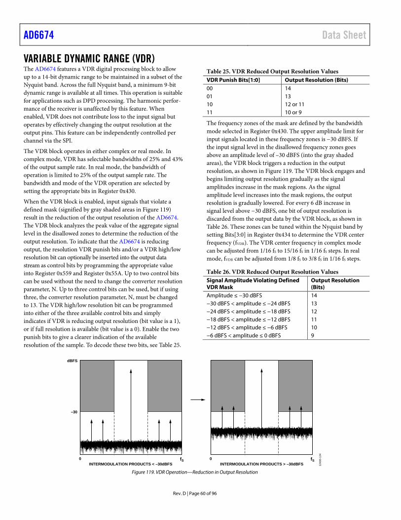
AD6674 Data Sheet
Rev. D | Page 60 of 96
VARIABLE DYNAMIC RANGE (VDR) The AD6674 features a VDR digital processing block to allow up to a 14-bit dynamic range to be maintained in a subset of the Nyquist band. Across the full Nyquist band, a minimum 9-bit dynamic range is available at all times. This operation is suitable for applications such as DPD processing. The harmonic perfor-mance of the receiver is unaffected by this feature. When enabled, VDR does not contribute loss to the input signal but operates by effectively changing the output resolution at the output pins. This feature can be independently controlled per channel via the SPI.
The VDR block operates in either complex or real mode. In complex mode, VDR has selectable bandwidths of 25% and 43% of the output sample rate. In real mode, the bandwidth of operation is limited to 25% of the output sample rate. The bandwidth and mode of the VDR operation are selected by setting the appropriate bits in Register 0x430.
When the VDR block is enabled, input signals that violate a defined mask (signified by gray shaded areas in Figure 119) result in the reduction of the output resolution of the AD6674. The VDR block analyzes the peak value of the aggregate signal level in the disallowed zones to determine the reduction of the output resolution. To indicate that the AD6674 is reducing output, the resolution VDR punish bits and/or a VDR high/low resolution bit can optionally be inserted into the output data stream as control bits by programming the appropriate value into Register 0x559 and Register 0x55A. Up to two control bits can be used without the need to change the converter resolution parameter, N. Up to three control bits can be used, but if using three, the converter resolution parameter, N, must be changed to 13. The VDR high/low resolution bit can be programmed into either of the three available control bits and simply indicates if VDR is reducing output resolution (bit value is a 1), or if full resolution is available (bit value is a 0). Enable the two punish bits to give a clearer indication of the available resolution of the sample. To decode these two bits, see Table 25.
Table 25. VDR Reduced Output Resolution Values VDR Punish Bits[1:0] Output Resolution (Bits) 00 14 01 13 10 12 or 11 11 10 or 9
The frequency zones of the mask are defined by the bandwidth mode selected in Register 0x430. The upper amplitude limit for input signals located in these frequency zones is −30 dBFS. If the input signal level in the disallowed frequency zones goes above an amplitude level of –30 dBFS (into the gray shaded areas), the VDR block triggers a reduction in the output resolution, as shown in Figure 119. The VDR block engages and begins limiting output resolution gradually as the signal amplitudes increase in the mask regions. As the signal amplitude level increases into the mask regions, the output resolution is gradually lowered. For every 6 dB increase in signal level above −30 dBFS, one bit of output resolution is discarded from the output data by the VDR block, as shown in Table 26. These zones can be tuned within the Nyquist band by setting Bits[3:0] in Register 0x434 to determine the VDR center frequency (fVDR). The VDR center frequency in complex mode can be adjusted from 1/16 fS to 15/16 fS in 1/16 fS steps. In real mode, fVDR can be adjusted from 1/8 fS to 3/8 fS in 1/16 fS steps.
Table 26. VDR Reduced Output Resolution Values Signal Amplitude Violating Defined VDR Mask
Output Resolution (Bits)
Amplitude ≤ −30 dBFS 14 −30 dBFS < amplitude ≤ −24 dBFS 13 −24 dBFS < amplitude ≤ −18 dBFS 12 −18 dBFS < amplitude ≤ −12 dBFS 11 −12 dBFS < amplitude ≤ −6 dBFS 10 −6 dBFS < amplitude ≤ 0 dBFS 9
dBFS
–30
0INTERMODULATION PRODUCTS < –30dBFS INTERMODULATION PRODUCTS > –30dBFS
fS 0 fS
1240
0-12
4
Figure 119. VDR Operation—Reduction in Output Resolution
Data Sheet AD6674
Rev. D | Page 61 of 96
VDR REAL MODE The real mode of VDR works over a bandwidth of 25% of the sample rate (50% of the Nyquist band). The output bandwidth of the AD6674 can be 25% only when operating in real mode. Figure 120 shows the frequency zones for the 25% bandwidth real output VDR mode tuned to a center frequency (fVDR) of fS/4 (tuning word = 0x04). The frequency zones where the amplitude may not exceed −30 dBFS are the upper and lower portions of the Nyquist band signified by the red shaded areas.
dBFS
–30
0 1/8 fS 3/8 fS 1/2 fS 1240
0-12
5
Figure 120. 25% VDR Bandwidth, Real Mode
The center frequency (fVDR) of the VDR function can be tuned within the Nyquist band from 1/8 fS to 3/8 fS in 1/16 fS steps. In real mode, Tuning Word 2 (0x02) through Tuning Word 6 (0x06) are valid. Table 27 shows the relative frequency values, and Table 28 shows the absolute frequency values based on a sample rate of 737.28 MSPS.
Table 27. VDR Tuning Words and Relative Frequency Values, 25% BW, Real Mode Tuning Word
Lower Band Edge
Center Frequency
Upper Band Edge
2 (0x02) 0 1/8 fS 1/4 fS 3 (0x03) 1/16 fS 3/16 fS 5/16 fS 4 (0x04) 1/8 fS 1/4 fS 3/8 fS 5 (0x05) 3/16 fS 5/16 fS 7/16 fS 6 (0x06) 1/4 fS 3/8 fS 1/2 fS
Table 28. VDR Tuning Words and Absolute Frequency Values, 25% BW, Real Mode with fS = 737.28 MSPS
Tuning Word
Lower Band Edge (MHz)
Center Frequency (MHz)
Upper Band Edge (MHz)
2 (0x02) 0 92.16 184.32 3 (0x03) 46.08 138.24 230.40 4 (0x04) 92.16 184.32 276.48 5 (0x05) 138.24 230.40 322.56 6 (0x06) 184.32 276.48 368.64
VDR COMPLEX MODE The complex mode of VDR works with selectable bandwidths of 25% of the sample rate (50% of the Nyquist band) and 43% of the sample rate (86% of the Nyquist band). Figure 121 and Figure 122 show the frequency zones for VDR in the complex mode. When operating VDR in complex mode, place I input signal data on Channel A and place Q input signal data on Channel B.
Figure 121 shows the frequency zones for the 25% bandwidth VDR mode with a center frequency of fS/4 (tuning word = 0x04). The frequency zones where the amplitude may not exceed –30 dBFS are the upper and lower portions of the Nyquist band extending into the complex domain.
–30
dBFS
1/8 fS 3/8 fS 1/2 fS–1/2 fS 0
1240
0-12
6
Figure 121. 25% VDR Bandwidth, Complex Mode
The center frequency (fVDR) of the VDR function can be tuned within the Nyquist band from 0 to 15/16 fS in 1/16 fS steps. In complex mode, Tuning Word 0 (0x00) through Tuning Word 15 (0x0F) are valid. Table 29 and Table 30 show the tuning words and frequency values for the 25% complex mode. Table 29 shows the relative frequency values, and Table 30 shows the absolute frequency values based on a sample rate of 737.28 MSPS.
Table 29. VDR Tuning Words and Relative Frequency Values, 25% BW, Complex Mode
Tuning Word Lower Band Edge
Center Frequency
Upper Band Edge
0 (0x00) –1/8 fS 0 1/8 fS 1 (0x01) –1/16 fS 1/16 fS 3/16 fS 2 (0x02) 0 1/8 fS 1/4 fS 3 (0x03) 1/16 fS 3/16 fS 5/16 fS 4 (0x04) 1/8 fS 1/4 fS 3/8 fS 5 (0x05) 3/16 fS 5/16 fS 7/16 fS 6 (0x06) 1/4 fS 3/8 fS 1/2 fS 7 (0x07) 5/16 fS 7/16 fS 9/16 fS 8 (0x08) 3/8 fS 1/2 fS 5/8 fS 9 (0x09) 7/16 fS 9/16 fS 11/16 fS 10 (0x0A) 1/2 fS 5/8 fS 3/4 fS 11 (0x0B) 9/16 fS 11/16 fS 13/16 fS 12 (0x0C) 5/8 fS 3/4 fS 7/8 fS 13 (0x0D) 11/16 fS 13/16 fS 15/16 fS 14 (0x0E) 3/4 fS 7/8 fS fS 15 (0x0F) 13/16 fS 15/16 fS 17/16 fS
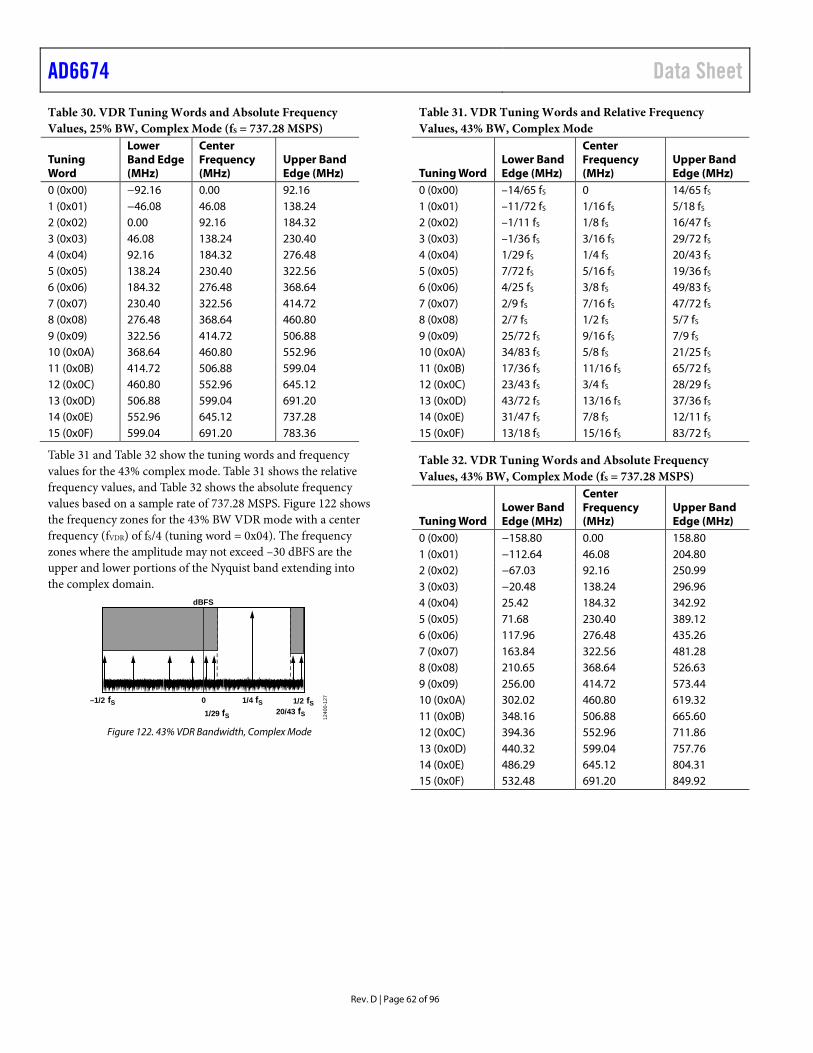
AD6674 Data Sheet
Rev. D | Page 62 of 96
Table 30. VDR Tuning Words and Absolute Frequency Values, 25% BW, Complex Mode (fS = 737.28 MSPS)
Tuning Word
Lower Band Edge (MHz)
Center Frequency (MHz)
Upper Band Edge (MHz)
0 (0x00) −92.16 0.00 92.16 1 (0x01) −46.08 46.08 138.24 2 (0x02) 0.00 92.16 184.32 3 (0x03) 46.08 138.24 230.40 4 (0x04) 92.16 184.32 276.48 5 (0x05) 138.24 230.40 322.56 6 (0x06) 184.32 276.48 368.64 7 (0x07) 230.40 322.56 414.72 8 (0x08) 276.48 368.64 460.80 9 (0x09) 322.56 414.72 506.88 10 (0x0A) 368.64 460.80 552.96 11 (0x0B) 414.72 506.88 599.04 12 (0x0C) 460.80 552.96 645.12 13 (0x0D) 506.88 599.04 691.20 14 (0x0E) 552.96 645.12 737.28 15 (0x0F) 599.04 691.20 783.36
Table 31 and Table 32 show the tuning words and frequency values for the 43% complex mode. Table 31 shows the relative frequency values, and Table 32 shows the absolute frequency values based on a sample rate of 737.28 MSPS. Figure 122 shows the frequency zones for the 43% BW VDR mode with a center frequency (fVDR) of fS/4 (tuning word = 0x04). The frequency zones where the amplitude may not exceed –30 dBFS are the upper and lower portions of the Nyquist band extending into the complex domain.
dBFS
1/29 fS
1/4 fS20/43 fS
1/2 fS–1/2 fS 0
1240
0-12
7
Figure 122. 43% VDR Bandwidth, Complex Mode
Table 31. VDR Tuning Words and Relative Frequency Values, 43% BW, Complex Mode
Tuning Word Lower Band Edge (MHz)
Center Frequency (MHz)
Upper Band Edge (MHz)
0 (0x00) –14/65 fS 0 14/65 fS 1 (0x01) –11/72 fS 1/16 fS 5/18 fS 2 (0x02) –1/11 fS 1/8 fS 16/47 fS 3 (0x03) –1/36 fS 3/16 fS 29/72 fS 4 (0x04) 1/29 fS 1/4 fS 20/43 fS 5 (0x05) 7/72 fS 5/16 fS 19/36 fS 6 (0x06) 4/25 fS 3/8 fS 49/83 fS 7 (0x07) 2/9 fS 7/16 fS 47/72 fS 8 (0x08) 2/7 fS 1/2 fS 5/7 fS 9 (0x09) 25/72 fS 9/16 fS 7/9 fS 10 (0x0A) 34/83 fS 5/8 fS 21/25 fS 11 (0x0B) 17/36 fS 11/16 fS 65/72 fS 12 (0x0C) 23/43 fS 3/4 fS 28/29 fS 13 (0x0D) 43/72 fS 13/16 fS 37/36 fS 14 (0x0E) 31/47 fS 7/8 fS 12/11 fS 15 (0x0F) 13/18 fS 15/16 fS 83/72 fS
Table 32. VDR Tuning Words and Absolute Frequency Values, 43% BW, Complex Mode (fS = 737.28 MSPS)
Tuning Word Lower Band Edge (MHz)
Center Frequency (MHz)
Upper Band Edge (MHz)
0 (0x00) −158.80 0.00 158.80 1 (0x01) −112.64 46.08 204.80 2 (0x02) −67.03 92.16 250.99 3 (0x03) −20.48 138.24 296.96 4 (0x04) 25.42 184.32 342.92 5 (0x05) 71.68 230.40 389.12 6 (0x06) 117.96 276.48 435.26 7 (0x07) 163.84 322.56 481.28 8 (0x08) 210.65 368.64 526.63 9 (0x09) 256.00 414.72 573.44 10 (0x0A) 302.02 460.80 619.32 11 (0x0B) 348.16 506.88 665.60 12 (0x0C) 394.36 552.96 711.86 13 (0x0D) 440.32 599.04 757.76 14 (0x0E) 486.29 645.12 804.31 15 (0x0F) 532.48 691.20 849.92
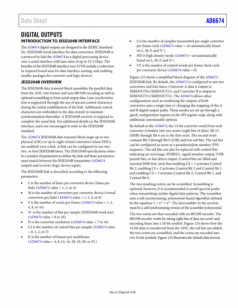
Data Sheet AD6674
Rev. D | Page 63 of 96
DIGITAL OUTPUTS INTRODUCTION TO JESD204B INTERFACE The AD6674 digital outputs are designed to the JEDEC Standard No. JESD204B serial interface for data converters. JESD204B is a protocol to link the AD6674 to a digital processing device over a serial interface with lane rates of up to 12.5 Gbps. The benefits of the JESD204B interface over LVDS include a reduction in required board area for data interface routing, and enabling smaller packages for converter and logic devices.
JESD204B OVERVIEW The JESD204B data transmit block assembles the parallel data from the ADC into frames and uses 8B/10B encoding as well as optional scrambling to form serial output data. Lane synchroniza-tion is supported through the use of special control characters during the initial establishment of the link. Additional control characters are embedded in the data stream to maintain synchronization thereafter. A JESD204B receiver is required to complete the serial link. For additional details on the JESD204B interface, users are encouraged to refer to the JESD204B standard.
The AD6674 JESD204B data transmit block maps up to two physical ADCs or up to eight virtual converters (when DDCs are enabled) over a link. A link can be configured to use one, two, or four JESD204B lanes. The JESD204B specification refers to a number of parameters to define the link and these parameters must match between the JESD204B transmitter (AD6674 output) and receiver (logic device input).
The JESD204B link is described according to the following parameters:
• L is the number of lanes per converter device (lanes per link) (AD6674 value = 1, 2, or 4)
• M is the number of converters per converter device (virtual converters per link) (AD6674 value = 1, 2, 4, or 8)
• F is the number of octets per frame (AD6674 value = 1, 2, 4, 8, or 16)
• N΄ is the number of bits per sample (JESD204B word size) (AD6674 value = 8 or 16)
• N is the converter resolution (AD6674 value = 7 to 16) • CS is the number of control bits per sample (AD6674 value
= 0, 1, 2, or 3) • K is the number of frames per multiframe
(AD6674 value = 4, 8, 12, 16, 20, 24, 28, or 32 )
• S is the number of samples transmitted per single converter per frame cycle (AD6674 value = set automatically based on L, M, F, and N΄)
• HD is high density mode (AD6674 = set automatically based on L, M, F, and N΄)
• CF is the number of control words per frame clock cycle per converter device (AD6674 value = 0)
Figure 123 shows a simplified block diagram of the AD6674 JESD204B link. By default, the AD6674 is configured to use two converters and four lanes. Converter A data is output to SERDOUT0±/SERDOUT1±, and Converter B is output to SERDOUT2±/SERDOUT3±. The AD6674 allows other configurations such as combining the outputs of both converters onto a single lane or changing the mapping of the A and B digital output paths. These modes are set up through a quick configuration register in the SPI register map, along with additional customizable options.
By default in the AD6674, the 14-bit converter word from each converter is broken into two octets (eight bits of data). Bit 13 (MSB) through Bit 6 are in the first octet. The second octet contains Bit 5 through Bit 0 (LSB) and two tail bits. The tail bits can be configured as zeros or a pseudorandom number (PN) sequence. The tail bits can also be replaced with control bits indicating an overrange, SYSREF±, signal monitor output, VDR punish bits, or fast detect output. Control bits are filled and inserted MSB first, such that enabling CS = 1 activates Control Bit 2, enabling CS = 2 activates Control Bit 2 and Control Bit 1, and enabling CS = 3 activates Control Bit 2, Control Bit 1, and Control Bit 0.
The two resulting octets can be scrambled. Scrambling is optional; however, it is recommended to avoid spectral peaks when transmitting similar digital data patterns. The scrambler uses a self synchronizing, polynomial-based algorithm defined by the equation 1 + x14 + x15. The descrambler in the receiver must be a self synchronizing version of the scrambler polynomial.
The two octets are then encoded with an 8B/10B encoder. The 8B/10B encoder works by taking eight bits of data (an octet) and encoding them into a 10-bit symbol. Figure 124 shows how the 14-bit data is transferred from the ADC, the tail bits are added, the two octets are scrambled, and the octets are encoded into two 10-bit symbols. Figure 124 illustrates the default data format.
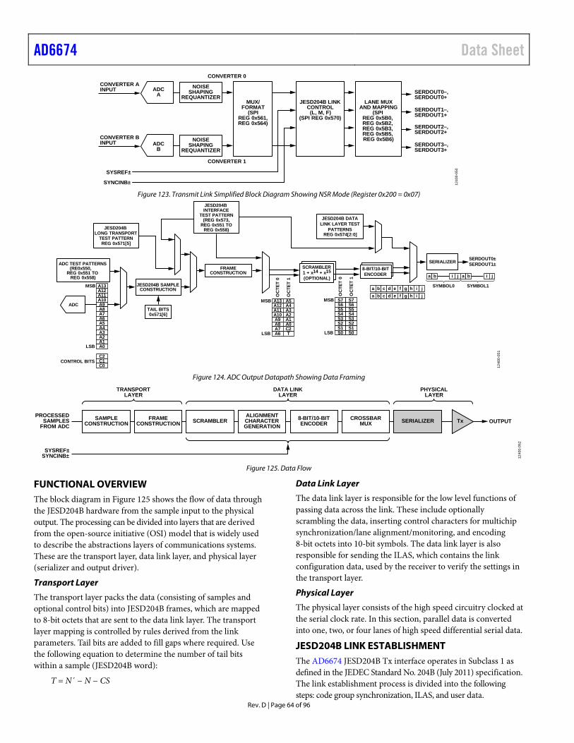
AD6674 Data Sheet
Rev. D | Page 64 of 96
ADCA
ADCB
SYSREF±
SYNCINB±
CONVERTER AINPUT
CONVERTER BINPUT
CONVERTER 0
CONVERTER 1
SERDOUT0–,SERDOUT0+
SERDOUT1–,SERDOUT1+
SERDOUT2–,SERDOUT2+
SERDOUT3–,SERDOUT3+
LANE MUXAND MAPPING
(SPIREG 0x5B0,REG 0x5B2,REG 0x5B3,REG 0x5B5,REG 0x5B6)
JESD204B LINKCONTROL
(L, M, F)(SPI REG 0x570)
MUX/FORMAT
(SPIREG 0x561,REG 0x564)
NOISESHAPING
REQUANTIZER
NOISESHAPING
REQUANTIZER
1240
0-05
0
Figure 123. Transmit Link Simplified Block Diagram Showing NSR Mode (Register 0x200 = 0x07)
8-BIT/10-BITENCODER
SERDOUT0±SERDOUT1±
TAIL BITS0x571[6]
SERIALIZER
ADC
SYMBOL0 SYMBOL1A13A12A11A10A9A8A7A6A5A4A3A2A1A0
C2C1C0
MSB
LSB
CONTROL BITS
ADC TEST PATTERNS(RE0x550,
REG 0x551 TOREG 0x558)
JESD204B SAMPLECONSTRUCTION
JESD204BINTERFACE
TEST PATTERN(REG 0x573,
REG 0x551 TOREG 0x558)
FRAMECONSTRUCTION
JESD204B DATALINK LAYER TEST
PATTERNSREG 0x574[2:0]
SCRAMBLER1 + x14 + x15(OPTIONAL)
A13A12A11A10A9A8A7A6
A5A4A3A2A1A0C2T
MSB
LSB
OC
TET
0
OC
TET
1
S7S6S5S4S3S2S1S0
S7S6S5S4S3S2S1S0
MSB
LSBO
CTE
T0
OC
TET
1
a b c d e f g h i ja b c d e f g h i j
a b i j a b i j
1240
0-05
1
JESD204BLONG TRANSPORT
TEST PATTERNREG 0x571[5]
Figure 124. ADC Output Datapath Showing Data Framing
TRANSPORTLAYER
PHYSICALLAYER
DATA LINKLAYER
Tx OUTPUTSAMPLECONSTRUCTION
FRAMECONSTRUCTION SCRAMBLER
ALIGNMENTCHARACTERGENERATION
8-BIT/10-BITENCODER
CROSSBARMUX SERIALIZER
PROCESSEDSAMPLES
FROM ADC
SYSREF±SYNCINB± 12
400-
052
Figure 125. Data Flow
FUNCTIONAL OVERVIEW The block diagram in Figure 125 shows the flow of data through the JESD204B hardware from the sample input to the physical output. The processing can be divided into layers that are derived from the open-source initiative (OSI) model that is widely used to describe the abstractions layers of communications systems. These are the transport layer, data link layer, and physical layer (serializer and output driver).
Transport Layer
The transport layer packs the data (consisting of samples and optional control bits) into JESD204B frames, which are mapped to 8-bit octets that are sent to the data link layer. The transport layer mapping is controlled by rules derived from the link parameters. Tail bits are added to fill gaps where required. Use the following equation to determine the number of tail bits within a sample (JESD204B word):
T = N΄ − N − CS
Data Link Layer
The data link layer is responsible for the low level functions of passing data across the link. These include optionally scrambling the data, inserting control characters for multichip synchronization/lane alignment/monitoring, and encoding 8-bit octets into 10-bit symbols. The data link layer is also responsible for sending the ILAS, which contains the link configuration data, used by the receiver to verify the settings in the transport layer.
Physical Layer
The physical layer consists of the high speed circuitry clocked at the serial clock rate. In this section, parallel data is converted into one, two, or four lanes of high speed differential serial data.
JESD204B LINK ESTABLISHMENT The AD6674 JESD204B Tx interface operates in Subclass 1 as defined in the JEDEC Standard No. 204B (July 2011) specification. The link establishment process is divided into the following steps: code group synchronization, ILAS, and user data.
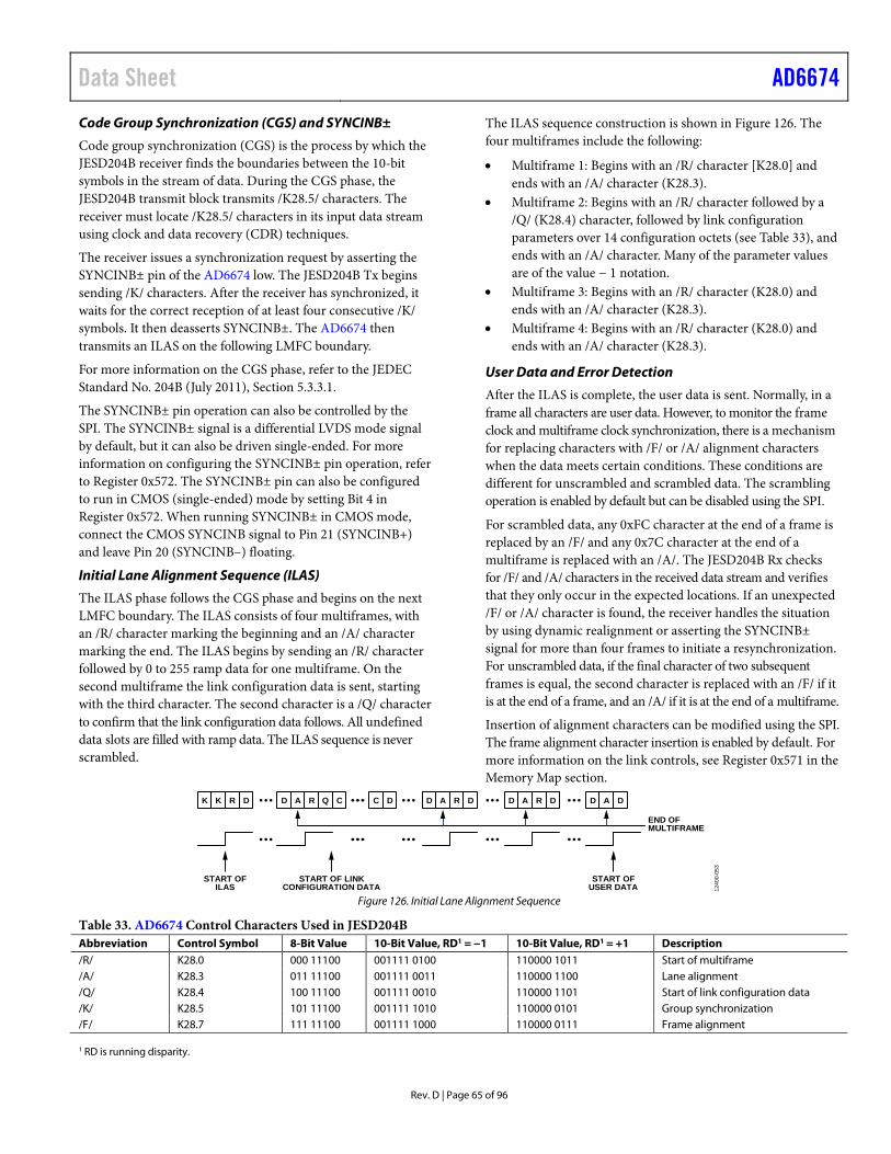
Data Sheet AD6674
Rev. D | Page 65 of 96
Code Group Synchronization (CGS) and SYNCINB±
Code group synchronization (CGS) is the process by which the JESD204B receiver finds the boundaries between the 10-bit symbols in the stream of data. During the CGS phase, the JESD204B transmit block transmits /K28.5/ characters. The receiver must locate /K28.5/ characters in its input data stream using clock and data recovery (CDR) techniques.
The receiver issues a synchronization request by asserting the SYNCINB± pin of the AD6674 low. The JESD204B Tx begins sending /K/ characters. After the receiver has synchronized, it waits for the correct reception of at least four consecutive /K/ symbols. It then deasserts SYNCINB±. The AD6674 then transmits an ILAS on the following LMFC boundary.
For more information on the CGS phase, refer to the JEDEC Standard No. 204B (July 2011), Section 5.3.3.1.
The SYNCINB± pin operation can also be controlled by the SPI. The SYNCINB± signal is a differential LVDS mode signal by default, but it can also be driven single-ended. For more information on configuring the SYNCINB± pin operation, refer to Register 0x572. The SYNCINB± pin can also be configured to run in CMOS (single-ended) mode by setting Bit 4 in Register 0x572. When running SYNCINB± in CMOS mode, connect the CMOS SYNCINB signal to Pin 21 (SYNCINB+) and leave Pin 20 (SYNCINB–) floating.
Initial Lane Alignment Sequence (ILAS)
The ILAS phase follows the CGS phase and begins on the next LMFC boundary. The ILAS consists of four multiframes, with an /R/ character marking the beginning and an /A/ character marking the end. The ILAS begins by sending an /R/ character followed by 0 to 255 ramp data for one multiframe. On the second multiframe the link configuration data is sent, starting with the third character. The second character is a /Q/ character to confirm that the link configuration data follows. All undefined data slots are filled with ramp data. The ILAS sequence is never scrambled.
The ILAS sequence construction is shown in Figure 126. The four multiframes include the following:
• Multiframe 1: Begins with an /R/ character [K28.0] and ends with an /A/ character (K28.3).
• Multiframe 2: Begins with an /R/ character followed by a /Q/ (K28.4) character, followed by link configuration parameters over 14 configuration octets (see Table 33), and ends with an /A/ character. Many of the parameter values are of the value − 1 notation.
• Multiframe 3: Begins with an /R/ character (K28.0) and ends with an /A/ character (K28.3).
• Multiframe 4: Begins with an /R/ character (K28.0) and ends with an /A/ character (K28.3).
User Data and Error Detection
After the ILAS is complete, the user data is sent. Normally, in a frame all characters are user data. However, to monitor the frame clock and multiframe clock synchronization, there is a mechanism for replacing characters with /F/ or /A/ alignment characters when the data meets certain conditions. These conditions are different for unscrambled and scrambled data. The scrambling operation is enabled by default but can be disabled using the SPI.
For scrambled data, any 0xFC character at the end of a frame is replaced by an /F/ and any 0x7C character at the end of a multiframe is replaced with an /A/. The JESD204B Rx checks for /F/ and /A/ characters in the received data stream and verifies that they only occur in the expected locations. If an unexpected /F/ or /A/ character is found, the receiver handles the situation by using dynamic realignment or asserting the SYNCINB± signal for more than four frames to initiate a resynchronization. For unscrambled data, if the final character of two subsequent frames is equal, the second character is replaced with an /F/ if it is at the end of a frame, and an /A/ if it is at the end of a multiframe.
Insertion of alignment characters can be modified using the SPI. The frame alignment character insertion is enabled by default. For more information on the link controls, see Register 0x571 in the Memory Map section.
K K R D D A R Q C C D D A R D D A R D D A D
START OFILAS
START OF LINKCONFIGURATION DATA
END OFMULTIFRAME
START OFUSER DATA 12
400-
053
Figure 126. Initial Lane Alignment Sequence
Table 33. AD6674 Control Characters Used in JESD204B Abbreviation Control Symbol 8-Bit Value 10-Bit Value, RD1 = −1 10-Bit Value, RD1 = +1 Description /R/ K28.0 000 11100 001111 0100 110000 1011 Start of multiframe /A/ K28.3 011 11100 001111 0011 110000 1100 Lane alignment /Q/ K28.4 100 11100 001111 0010 110000 1101 Start of link configuration data /K/ K28.5 101 11100 001111 1010 110000 0101 Group synchronization /F/ K28.7 111 11100 001111 1000 110000 0111 Frame alignment 1 RD is running disparity.
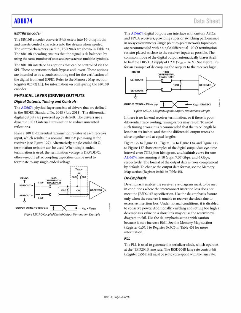
AD6674 Data Sheet
Rev. D | Page 66 of 96
8B/10B Encoder
The 8B/10B encoder converts 8-bit octets into 10-bit symbols and inserts control characters into the stream when needed. The control characters used in JESD204B are shown in Table 33. The 8B/10B encoding ensures that the signal is dc balanced by using the same number of ones and zeros across multiple symbols.
The 8B/10B interface has options that can be controlled via the SPI. These operations include bypass and invert. These options are intended to be a troubleshooting tool for the verification of the digital front end (DFE). Refer to the Memory Map section, Register 0x572[2:1], for information on configuring the 8B/10B encoder.
PHYSICAL LAYER (DRIVER) OUTPUTS Digital Outputs, Timing and Controls
The AD6674 physical layer consists of drivers that are defined in the JEDEC Standard No. 204B (July 2011). The differential digital outputs are powered up by default. The drivers use a dynamic 100 Ω internal termination to reduce unwanted reflections.
Place a 100 Ω differential termination resistor at each receiver input, which results in a nominal 300 mV p-p swing at the receiver (see Figure 127). Alternatively, single-ended 50 Ω termination resistors can be used. When single-ended termination is used, the termination voltage is DRVDD/2; otherwise, 0.1 μF ac coupling capacitors can be used to terminate to any single-ended voltage.
OR
SERDOUTx+
DRVDD
VRXCM
SERDOUTx–
OUTPUT SWING = 300mV p-p
0.1µF
100Ω
50Ω50Ω
0.1µF
RECEIVER
VCM = VRXCM
100ΩDIFFERENTIALTRACE PAIR
1240
0-05
4
Figure 127. AC-Coupled Digital Output Termination Example
The AD6674 digital outputs can interface with custom ASICs and FPGA receivers, providing superior switching performance in noisy environments. Single point-to-point network topologies are recommended with a single differential 100 Ω termination resistor placed as close to the receiver inputs as possible. The common mode of the digital output automatically biases itself to half the DRVDD supply of 1.2 V (VCM = 0.6 V). See Figure 128 for an example of dc coupling the outputs to the receiver logic.
SERDOUTx+
DRVDD
SERDOUTx–
OUTPUT SWING = 300mV p-p
100Ω RECEIVER
VCM = DRVDD/2
100ΩDIFFERENTIALTRACE PAIR
1240
0-05
5
Figure 128. DC-Coupled Digital Output Termination Example
If there is no far-end receiver termination, or if there is poor differential trace routing, timing errors may result. To avoid such timing errors, it is recommended that the trace length be less than six inches, and that the differential output traces be close together and at equal lengths.
Figure 129 to Figure 131, Figure 132 to Figure 134, and Figure 135 to Figure 137 show examples of the digital output data eye, time interval error (TIE) jitter histogram, and bathtub curve for one AD6674 lane running at 10 Gbps, 7.37 Gbps, and 6 Gbps, respectively. The format of the output data is twos complement by default. To change the output data format, see the Memory Map section (Register 0x561 in Table 45).
De-Emphasis
De-emphasis enables the receiver eye diagram mask to be met in conditions where the interconnect insertion loss does not meet the JESD204B specification. Use the de-emphasis feature only when the receiver is unable to recover the clock due to excessive insertion loss. Under normal conditions, it is disabled to conserve power. Additionally, enabling and setting too high a de-emphasis value on a short link may cause the receiver eye diagram to fail. Use the de-emphasis setting with caution because it may increase EMI. See the Memory Map section (Register 0x5C1 to Register 0x5C5 in Table 45) for more information.
PLL
The PLL is used to generate the serializer clock, which operates at the JESD204B lane rate. The JESD204B lane rate control bit (Register 0x56E[4]) must be set to correspond with the lane rate.
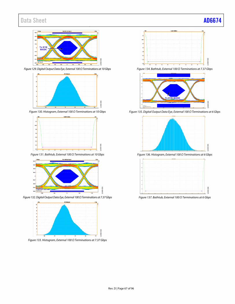
Data Sheet AD6674
Rev. D | Page 67 of 96
Tx EYEMASK
1240
0-58
8
Figure 129. Digital Output Data Eye, External 100 Ω Terminations at 10 Gbps
1240
0-58
9
Figure 130. Histogram, External 100 Ω Terminations at 10 Gbps
1240
0-59
0
Figure 131. Bathtub, External 100 Ω Terminations at 10 Gbps
1240
0-59
1
Figure 132. Digital Output Data Eye, External 100 Ω Terminations at 7.37 Gbps
1240
0-59
2
Figure 133. Histogram, External 100 Ω Terminations at 7.37 Gbps
1240
0-59
3
Figure 134. Bathtub, External 100 Ω Terminations at 7.37 Gbps
Tx EYE MASK
1240
0-59
4
Figure 135. Digital Output Data Eye, External 100 Ω Terminations at 6 Gbps
1240
0-59
5
Figure 136. Histogram, External 100 Ω Terminations at 6 Gbps
1240
0-59
6
Figure 137. Bathtub, External 100 Ω Terminations at 6 Gbps
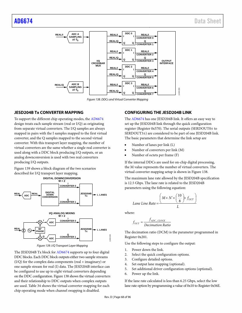
AD6674 Data Sheet
Rev. D | Page 68 of 96
DDC 0I
Q
I
Q
REAL/ICONVERTER 0
QCONVERTER 1
REAL/I
REAL/Q
DDC 1I
Q
I
Q
REAL/ICONVERTER 2
QCONVERTER 3
REAL/I
REAL/Q
DDC 2I
Q
I
Q
REAL/ICONVERTER 4
QCONVERTER 5
REAL/I
REAL/Q
DDC 3I
Q
I
Q
REAL/ICONVERTER 6
QCONVERTER 7
REAL/I
REAL/Q
OUTPUTINTERFACE
I/QCROSSBAR
MUX
ADC ASAMPLING
AT fS
REAL/I
ADC BSAMPLING
AT fS
REAL/Q
1240
0-05
9
Figure 138. DDCs and Virtual Converter Mapping
JESD204B Tx CONVERTER MAPPING To support the different chip operating modes, the AD6674 design treats each sample stream (real or I/Q) as originating from separate virtual converters. The I/Q samples are always mapped in pairs with the I samples mapped to the first virtual converter, and the Q samples mapped to the second virtual converter. With this transport layer mapping, the number of virtual converters are the same whether a single real converter is used along with a DDC block producing I/Q outputs, or an analog downconversion is used with two real converters producing I/Q outputs.
Figure 139 shows a block diagram of the two scenarios described for I/Q transport layer mapping.
REAL
I
Q
ICONVERTER 0
QCONVERTER 1
ADC
ADC
90°PHASEΣ JESD204B
Tx L LANES
I/Q ANALOG MIXINGM = 2
ADCREAL REAL
ICONVERTER 0
QCONVERTER 1
JESD204BTx L LANES
DIGITAL DOWNCONVERSIONM = 2
DIGITALDOWN
CONVERSION
1240
0-05
8
Figure 139. I/Q Transport Layer Mapping
The JESD204B Tx block for AD6674 supports up to four digital DDC blocks. Each DDC block outputs either two sample streams (I/Q) for the complex data components (real + imaginary) or one sample stream for real (I) data. The JESD204B interface can be configured to use up to eight virtual converters depending on the DDC configuration. Figure 138 shows the virtual converters and their relationship to DDC outputs when complex outputs are used. Table 34 shows the virtual converter mapping for each chip operating mode when channel swapping is disabled.
CONFIGURING THE JESD204B LINK The AD6674 has one JESD204B link. It offers an easy way to set up the JESD204B link through the quick configuration register (Register 0x570). The serial outputs (SERDOUT0± to SERDOUT3±) are considered to be part of one JESD204B link. The basic parameters that determine the link setup are
• Number of lanes per link (L) • Number of converters per link (M) • Number of octets per frame (F)
If the internal DDCs are used for on-chip digital processing, the M value represents the number of virtual converters. The virtual converter mapping setup is shown in Figure 138.
The maximum lane rate allowed by the JESD204B specification is 12.5 Gbps. The lane rate is related to the JESD204B parameters using the following equation:
L
fNMRateLineLane
OUT
×
××
= 810'
where:
RatioDecimationf
f CLOCKADCOUT
_=
The decimation ratio (DCM) is the parameter programmed in Register 0x201.
Use the following steps to configure the output:
1. Power down the link. 2. Select the quick configuration options. 3. Configure detailed options. 4. Set output lane mapping (optional). 5. Set additional driver configuration options (optional). 6. Power up the link.
If the lane rate calculated is less than 6.25 Gbps, select the low lane rate option by programming a value of 0x10 to Register 0x56E.
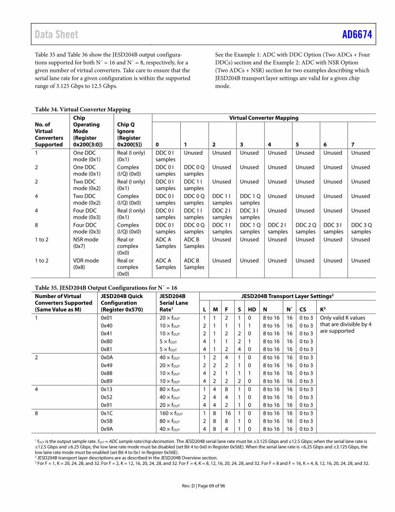
Data Sheet AD6674
Rev. D | Page 69 of 96
Table 35 and Table 36 show the JESD204B output configura-tions supported for both N΄ = 16 and N΄ = 8, respectively, for a given number of virtual converters. Take care to ensure that the serial lane rate for a given configuration is within the supported range of 3.125 Gbps to 12.5 Gbps.
See the Example 1: ADC with DDC Option (Two ADCs + Four DDCs) section and the Example 2: ADC with NSR Option (Two ADCs + NSR) section for two examples describing which JESD204B transport layer settings are valid for a given chip mode.
Table 34. Virtual Converter Mapping
No. of Virtual Converters Supported
Chip Operating Mode (Register 0x200[3:0])
Chip Q Ignore (Register 0x200[5])
Virtual Converter Mapping
0 1 2 3 4 5 6 7 1 One DDC
mode (0x1) Real (I only) (0x1)
DDC 0 I samples
Unused Unused Unused Unused Unused Unused Unused
2 One DDC mode (0x1)
Complex (I/Q) (0x0)
DDC 0 I samples
DDC 0 Q samples
Unused Unused Unused Unused Unused Unused
2 Two DDC mode (0x2)
Real (I only) (0x1)
DDC 0 I samples
DDC 1 I samples
Unused Unused Unused Unused Unused Unused
4 Two DDC mode (0x2)
Complex (I/Q) (0x0)
DDC 0 I samples
DDC 0 Q samples
DDC 1 I samples
DDC 1 Q samples
Unused Unused Unused Unused
4 Four DDC mode (0x3)
Real (I only) (0x1)
DDC 0 I samples
DDC 1 I samples
DDC 2 I samples
DDC 3 I samples
Unused Unused Unused Unused
8 Four DDC mode (0x3)
Complex (I/Q) (0x0)
DDC 0 I samples
DDC 0 Q samples
DDC 1 I samples
DDC 1 Q samples
DDC 2 I samples
DDC 2 Q samples
DDC 3 I samples
DDC 3 Q samples
1 to 2 NSR mode (0x7)
Real or complex (0x0)
ADC A Samples
ADC B Samples
Unused Unused Unused Unused Unused Unused
1 to 2 VDR mode (0x8)
Real or complex (0x0)
ADC A Samples
ADC B Samples
Unused Unused Unused Unused Unused Unused
Table 35. JESD204B Output Configurations for N΄ = 16 Number of Virtual Converters Supported (Same Value as M)
JESD204B Quick Configuration (Register 0x570)
JESD204B Serial Lane Rate1
JESD204B Transport Layer Settings2
L M F S HD N N΄ CS K3 1 0x01 20 × fOUT 1 1 2 1 0 8 to 16 16 0 to 3 Only valid K values
that are divisible by 4 are supported
0x40 10 × fOUT 2 1 1 1 1 8 to 16 16 0 to 3 0x41 10 × fOUT 2 1 2 2 0 8 to 16 16 0 to 3 0x80 5 × fOUT 4 1 1 2 1 8 to 16 16 0 to 3 0x81 5 × fOUT 4 1 2 4 0 8 to 16 16 0 to 3 2 0x0A 40 × fOUT 1 2 4 1 0 8 to 16 16 0 to 3 0x49 20 × fOUT 2 2 2 1 0 8 to 16 16 0 to 3 0x88 10 × fOUT 4 2 1 1 1 8 to 16 16 0 to 3 0x89 10 × fOUT 4 2 2 2 0 8 to 16 16 0 to 3 4 0x13 80 × fOUT 1 4 8 1 0 8 to 16 16 0 to 3 0x52 40 × fOUT 2 4 4 1 0 8 to 16 16 0 to 3 0x91 20 × fOUT 4 4 2 1 0 8 to 16 16 0 to 3 8 0x1C 160 × fOUT 1 8 16 1 0 8 to 16 16 0 to 3 0x5B 80 × fOUT 2 8 8 1 0 8 to 16 16 0 to 3 0x9A 40 × fOUT 4 8 4 1 0 8 to 16 16 0 to 3 1 fOUT is the output sample rate. fOUT = ADC sample rate/chip decimation. The JESD204B serial lane rate must be ≥3.125 Gbps and ≤12.5 Gbps; when the serial lane rate is ≤12.5 Gbps and ≥6.25 Gbps, the low lane rate mode must be disabled (set Bit 4 to 0x0 in Register 0x56E). When the serial lane rate is <6.25 Gbps and ≥3.125 Gbps, the low lane rate mode must be enabled (set Bit 4 to 0x1 in Register 0x56E). 2 JESD204B transport layer descriptions are as described in the JESD204B Overview section. 3 For F = 1, K = 20, 24, 28, and 32. For F = 2, K = 12, 16, 20, 24, 28, and 32. For F = 4, K = 8, 12, 16, 20, 24, 28, and 32. For F = 8 and F = 16, K = 4, 8, 12, 16, 20, 24, 28, and 32.
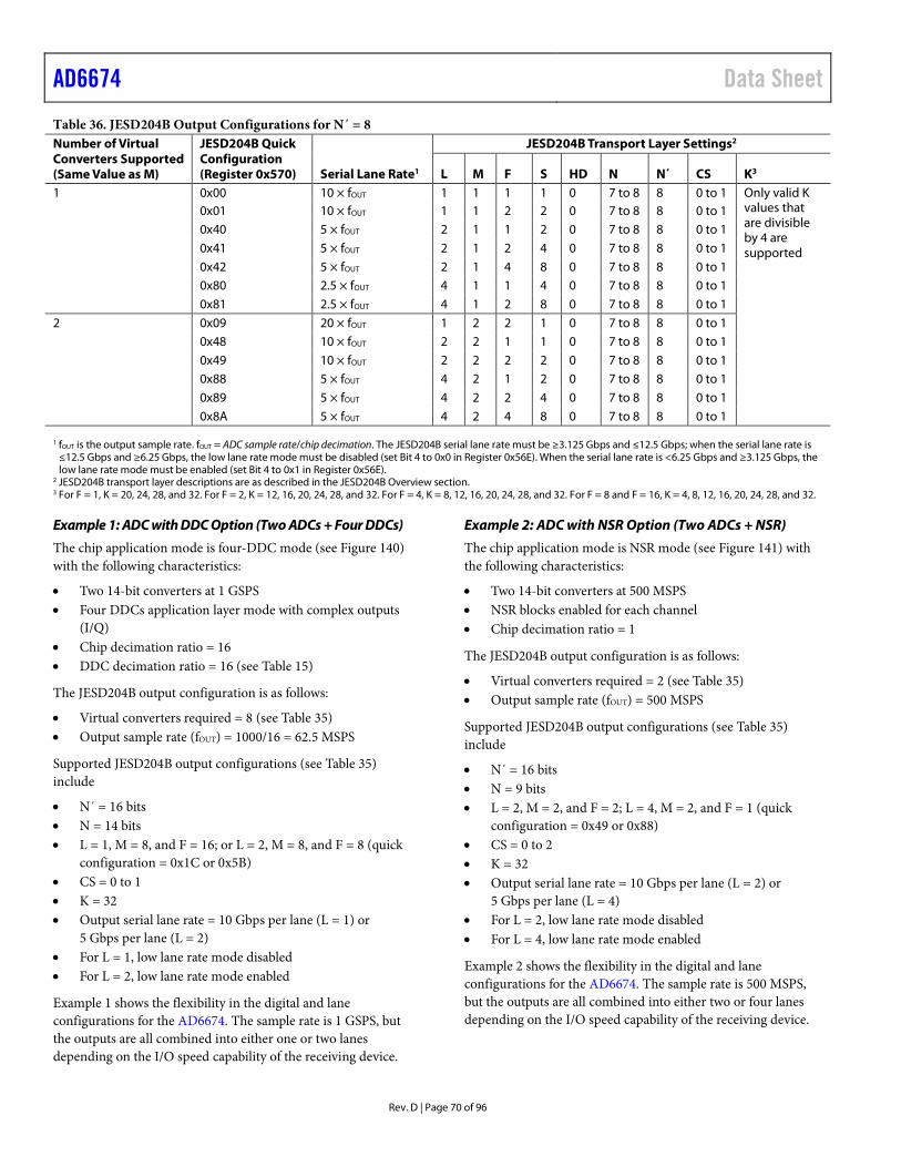
AD6674 Data Sheet
Rev. D | Page 70 of 96
Table 36. JESD204B Output Configurations for N΄ = 8 Number of Virtual Converters Supported (Same Value as M)
JESD204B Quick Configuration (Register 0x570) Serial Lane Rate1
JESD204B Transport Layer Settings2
L M F S HD N N΄ CS K3 1 0x00 10 × fOUT 1 1 1 1 0 7 to 8 8 0 to 1 Only valid K
values that are divisible by 4 are supported
0x01 10 × fOUT 1 1 2 2 0 7 to 8 8 0 to 1 0x40 5 × fOUT 2 1 1 2 0 7 to 8 8 0 to 1 0x41 5 × fOUT 2 1 2 4 0 7 to 8 8 0 to 1 0x42 5 × fOUT 2 1 4 8 0 7 to 8 8 0 to 1 0x80 2.5 × fOUT 4 1 1 4 0 7 to 8 8 0 to 1 0x81 2.5 × fOUT 4 1 2 8 0 7 to 8 8 0 to 1 2 0x09 20 × fOUT 1 2 2 1 0 7 to 8 8 0 to 1 0x48 10 × fOUT 2 2 1 1 0 7 to 8 8 0 to 1 0x49 10 × fOUT 2 2 2 2 0 7 to 8 8 0 to 1 0x88 5 × fOUT 4 2 1 2 0 7 to 8 8 0 to 1 0x89 5 × fOUT 4 2 2 4 0 7 to 8 8 0 to 1 0x8A 5 × fOUT 4 2 4 8 0 7 to 8 8 0 to 1 1 fOUT is the output sample rate. fOUT = ADC sample rate/chip decimation. The JESD204B serial lane rate must be ≥3.125 Gbps and ≤12.5 Gbps; when the serial lane rate is
≤12.5 Gbps and ≥6.25 Gbps, the low lane rate mode must be disabled (set Bit 4 to 0x0 in Register 0x56E). When the serial lane rate is <6.25 Gbps and ≥3.125 Gbps, the low lane rate mode must be enabled (set Bit 4 to 0x1 in Register 0x56E).
2 JESD204B transport layer descriptions are as described in the JESD204B Overview section. 3 For F = 1, K = 20, 24, 28, and 32. For F = 2, K = 12, 16, 20, 24, 28, and 32. For F = 4, K = 8, 12, 16, 20, 24, 28, and 32. For F = 8 and F = 16, K = 4, 8, 12, 16, 20, 24, 28, and 32.
Example 1: ADC with DDC Option (Two ADCs + Four DDCs)
The chip application mode is four-DDC mode (see Figure 140) with the following characteristics:
• Two 14-bit converters at 1 GSPS • Four DDCs application layer mode with complex outputs
(I/Q) • Chip decimation ratio = 16 • DDC decimation ratio = 16 (see Table 15)
The JESD204B output configuration is as follows:
• Virtual converters required = 8 (see Table 35) • Output sample rate (fOUT) = 1000/16 = 62.5 MSPS
Supported JESD204B output configurations (see Table 35) include
• N΄ = 16 bits • N = 14 bits • L = 1, M = 8, and F = 16; or L = 2, M = 8, and F = 8 (quick
configuration = 0x1C or 0x5B) • CS = 0 to 1 • K = 32 • Output serial lane rate = 10 Gbps per lane (L = 1) or
5 Gbps per lane (L = 2) • For L = 1, low lane rate mode disabled • For L = 2, low lane rate mode enabled
Example 1 shows the flexibility in the digital and lane configurations for the AD6674. The sample rate is 1 GSPS, but the outputs are all combined into either one or two lanes depending on the I/O speed capability of the receiving device.
Example 2: ADC with NSR Option (Two ADCs + NSR)
The chip application mode is NSR mode (see Figure 141) with the following characteristics:
• Two 14-bit converters at 500 MSPS • NSR blocks enabled for each channel • Chip decimation ratio = 1
The JESD204B output configuration is as follows:
• Virtual converters required = 2 (see Table 35) • Output sample rate (fOUT) = 500 MSPS
Supported JESD204B output configurations (see Table 35) include
• N΄ = 16 bits • N = 9 bits • L = 2, M = 2, and F = 2; L = 4, M = 2, and F = 1 (quick
configuration = 0x49 or 0x88) • CS = 0 to 2 • K = 32 • Output serial lane rate = 10 Gbps per lane (L = 2) or
5 Gbps per lane (L = 4) • For L = 2, low lane rate mode disabled • For L = 4, low lane rate mode enabled
Example 2 shows the flexibility in the digital and lane configurations for the AD6674. The sample rate is 500 MSPS, but the outputs are all combined into either two or four lanes depending on the I/O speed capability of the receiving device.
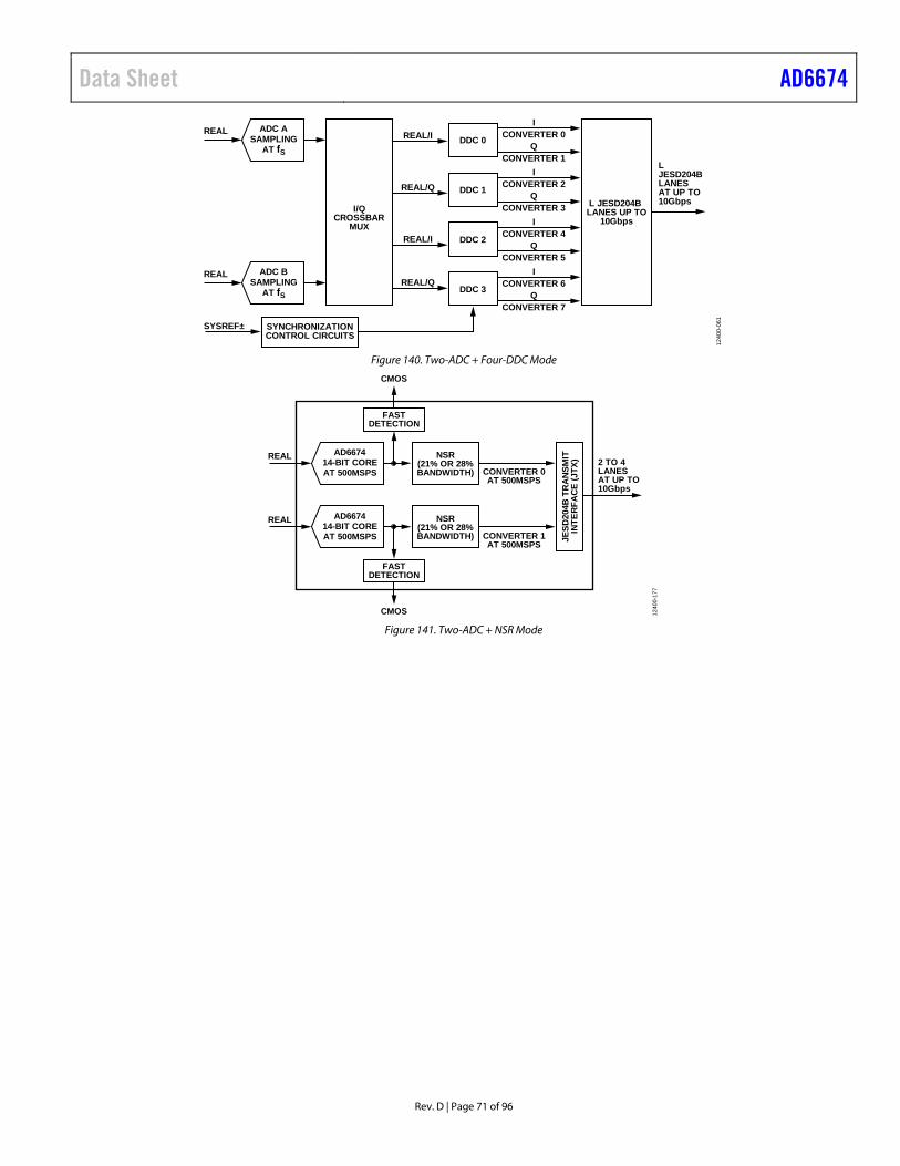
Data Sheet AD6674
Rev. D | Page 71 of 96
DDC 0
ICONVERTER 0
QCONVERTER 1
REAL/I
DDC 1
ICONVERTER 2
QCONVERTER 3
REAL/Q
DDC 2
ICONVERTER 4
QCONVERTER 5
REAL/I
DDC 3
ICONVERTER 6
QCONVERTER 7
REAL/Q
I/QCROSSBAR
MUX
ADC ASAMPLING
AT fS
REAL
ADC BSAMPLING
AT fS
REAL
SYNCHRONIZATIONCONTROL CIRCUITS
SYSREF±
L JESD204BLANES UP TO
10Gbps
LJESD204BLANESAT UP TO10Gbps
1240
0-06
1
Figure 140. Two-ADC + Four-DDC Mode
JESD
204B
TR
AN
SMIT
INTE
RFA
CE
(JTX
)NSR(21% OR 28%BANDWIDTH)
NSR(21% OR 28%BANDWIDTH)
FASTDETECTION
FASTDETECTION
CMOS
CMOS
CONVERTER 0AT 500MSPS
CONVERTER 1AT 500MSPS
REAL
2 TO 4LANESAT UP TO10Gbps
AD667414-BIT COREAT 500MSPS
AD667414-BIT COREAT 500MSPS
REAL
1240
0-17
7
Figure 141. Two-ADC + NSR Mode
AD6674 Data Sheet
Rev. D | Page 72 of 96
MULTICHIP SYNCHRONIZATION The AD6674 has a SYSREF± input that allows the user flexible options for synchronizing the internal blocks. The SYSREF± input is a source synchronous system reference signal that enables multichip synchronization. The input clock divider, DDCs, signal monitor block, and JESD204B link can be synchronized using the SYSREF± input. For the highest level of timing accuracy, SYSREF± must meet setup and hold require-ments relative to the CLK± input.
The flowchart in Figure 142 describes the internal mechanism by which multichip synchronization can be achieved in the
AD6674. The AD6674 supports several features that aid users in meeting the requirements for capturing a SYSREF± signal. The SYSREF± sample event is defined as either a synchronous low to high transition or a synchronous high to low transition. Addition-ally, the AD6674 allows the SYSREF± signal to be sampled using either the rising edge or falling edge of the CLK± input. The AD6674 also has the ability to ignore a programmable number (up to 16) of SYSREF± events. The SYSREF± control options can be selected using Register 0x120 and Register 0x121.
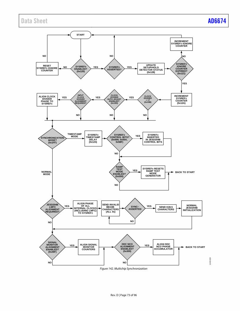
Data Sheet AD6674
Rev. D | Page 73 of 96
YESUPDATE
SETUP/HOLDDETECTOR STATUS
(0x128)
INCREMENTSYSREF± IGNORE
COUNTER
YES
NO
SYSREF±ENABLED?
(0x120)
NO
CLOCKDIVIDER
> 1?(0x10B)
YES
NO
INPUTCLOCKDIVIDER
ALIGNMENTREQUIRED?
YES
NONO
YESALIGN CLOCKDIVIDER
PHASE TOSYSREF±
SYNCHRONIZATIONMODE?(0x1FF)
TIMESTAMPMODE
NORMALMODE
YES SYSREF±INSERTED
IN JESD204BCONTROL BITS
BACK TO START
NO
DDC NCOALIGNMENTENABLED?
(0x300)
YES
NO NO
YES SEND K28.5CHARACTERS
NORMALJESD204B
INITIALIZATION
SYSREF±CONTROL BITS?
(0x559, 0x55A,0x58F)
RESETSYSREF± IGNORE
COUNTER
NO
START
SYSREF±ASSERTED?
YES
NO
YESALIGN SIGNALMONITOR
COUNTERSYES
NO NO
YES
NO
INCREMENTSYSREF±COUNTER
(0x12A)
SYSREF±TIMESTAMP
DELAY(0x123)
BACK TO START
SYSREF±IGNORE
COUNTEREXPIRED?
(0x121)
CLOCKDIVIDER
AUTO ADJUSTENABLED?
(0x10D)
RAMPTESTMODE
ENABLED?(0x550)
SYSREF± RESETSRAMP TEST
MODEGENERATOR
JESD204BLMFC
ALIGNMENTREQUIRED?
ALIGN PHASEOF ALL
INTERNAL CLOCKS(INCLUDING LMFC)
TO SYSREF±
SEND INVALID8B/10B
CHARACTERS(ALL 0s)
SYNC~ASSERTED
SIGNALMONITOR
ALIGNMENTENABLED?
(0x26F)
ALIGN DDCNCO PHASE
ACCUMULATOR
1240
0-50
9
Figure 142. Multichip Synchronization
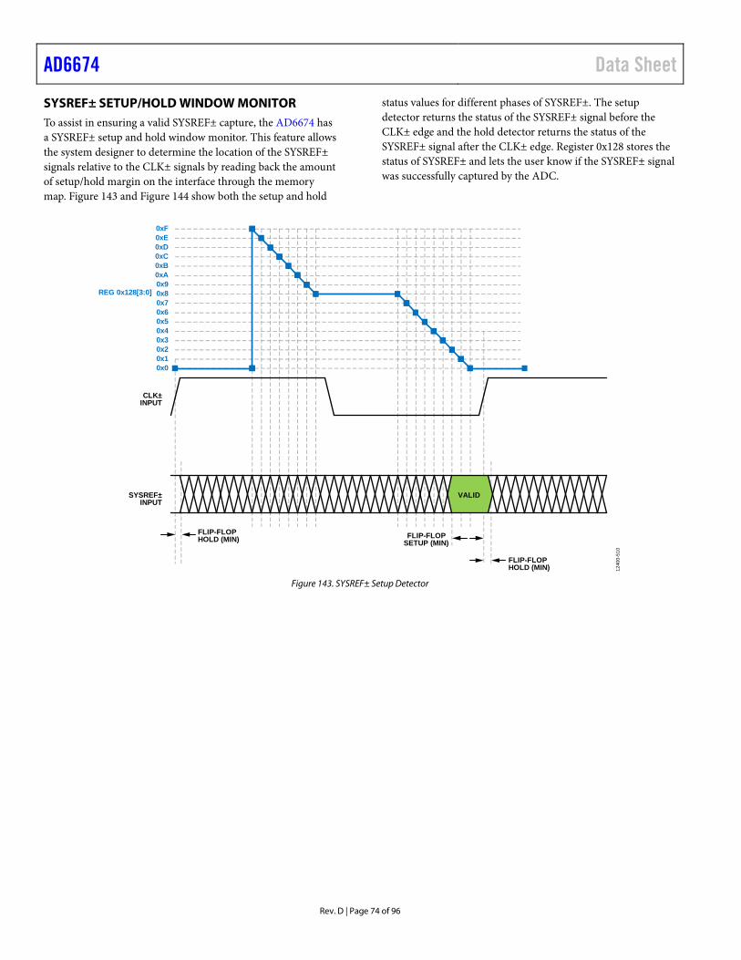
AD6674 Data Sheet
Rev. D | Page 74 of 96
SYSREF± SETUP/HOLD WINDOW MONITOR To assist in ensuring a valid SYSREF± capture, the AD6674 has a SYSREF± setup and hold window monitor. This feature allows the system designer to determine the location of the SYSREF± signals relative to the CLK± signals by reading back the amount of setup/hold margin on the interface through the memory map. Figure 143 and Figure 144 show both the setup and hold
status values for different phases of SYSREF±. The setup detector returns the status of the SYSREF± signal before the CLK± edge and the hold detector returns the status of the SYSREF± signal after the CLK± edge. Register 0x128 stores the status of SYSREF± and lets the user know if the SYSREF± signal was successfully captured by the ADC.
VALID
0xF0xE0xD0xC0xB0xA0x90x80x70x60x50x40x30x20x10x0
REG 0x128[3:0]
CLK±INPUT
SYSREF±INPUT
FLIP-FLOPHOLD (MIN)
FLIP-FLOPHOLD (MIN)
FLIP-FLOPSETUP (MIN)
1240
0-51
0
Figure 143. SYSREF± Setup Detector
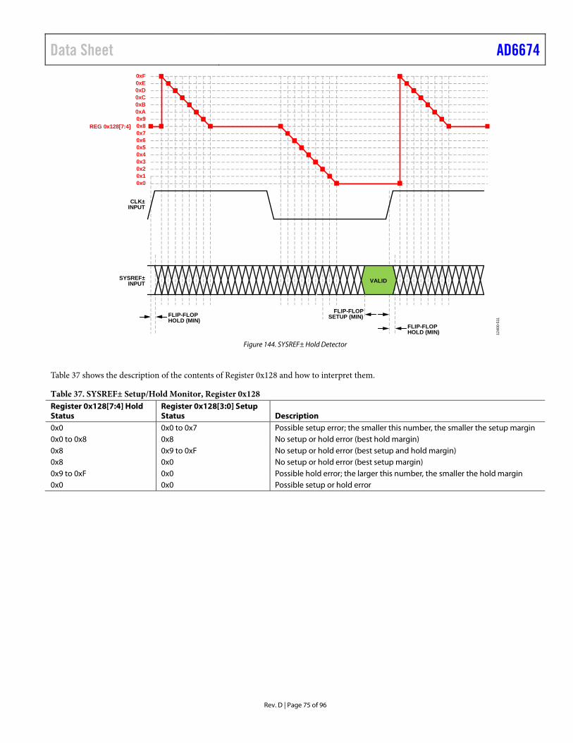
Data Sheet AD6674
Rev. D | Page 75 of 96
CLK±INPUT
SYSREF±INPUT VALID
REG 0x128[7:4]
FLIP-FLOPHOLD (MIN)
FLIP-FLOPHOLD (MIN)
FLIP-FLOPSETUP (MIN)
1240
0-51
1
0xF0xE0xD0xC0xB0xA0x90x80x70x60x50x40x30x20x10x0
Figure 144. SYSREF± Hold Detector
Table 37 shows the description of the contents of Register 0x128 and how to interpret them.
Table 37. SYSREF± Setup/Hold Monitor, Register 0x128 Register 0x128[7:4] Hold Status
Register 0x128[3:0] Setup Status Description
0x0 0x0 to 0x7 Possible setup error; the smaller this number, the smaller the setup margin 0x0 to 0x8 0x8 No setup or hold error (best hold margin) 0x8 0x9 to 0xF No setup or hold error (best setup and hold margin) 0x8 0x0 No setup or hold error (best setup margin) 0x9 to 0xF 0x0 Possible hold error; the larger this number, the smaller the hold margin 0x0 0x0 Possible setup or hold error
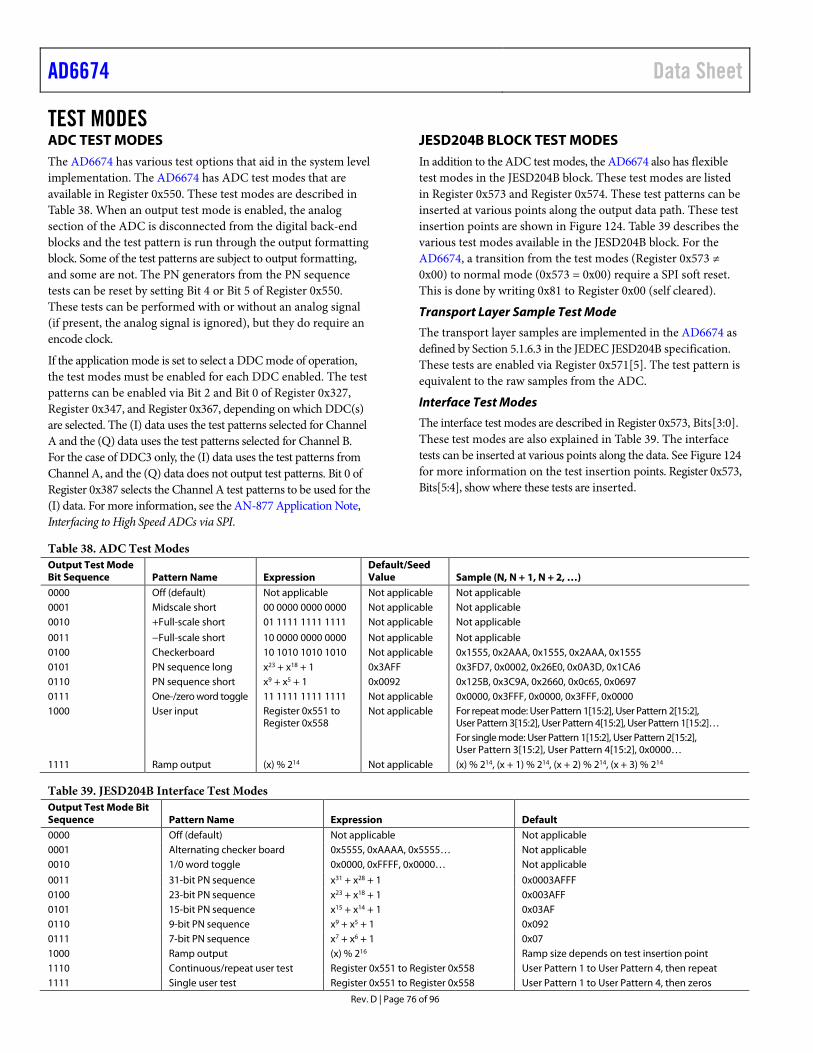
AD6674 Data Sheet
Rev. D | Page 76 of 96
TEST MODES ADC TEST MODES The AD6674 has various test options that aid in the system level implementation. The AD6674 has ADC test modes that are available in Register 0x550. These test modes are described in Table 38. When an output test mode is enabled, the analog section of the ADC is disconnected from the digital back-end blocks and the test pattern is run through the output formatting block. Some of the test patterns are subject to output formatting, and some are not. The PN generators from the PN sequence tests can be reset by setting Bit 4 or Bit 5 of Register 0x550. These tests can be performed with or without an analog signal (if present, the analog signal is ignored), but they do require an encode clock.
If the application mode is set to select a DDC mode of operation, the test modes must be enabled for each DDC enabled. The test patterns can be enabled via Bit 2 and Bit 0 of Register 0x327, Register 0x347, and Register 0x367, depending on which DDC(s) are selected. The (I) data uses the test patterns selected for Channel A and the (Q) data uses the test patterns selected for Channel B. For the case of DDC3 only, the (I) data uses the test patterns from Channel A, and the (Q) data does not output test patterns. Bit 0 of Register 0x387 selects the Channel A test patterns to be used for the (I) data. For more information, see the AN-877 Application Note, Interfacing to High Speed ADCs via SPI.
JESD204B BLOCK TEST MODES In addition to the ADC test modes, the AD6674 also has flexible test modes in the JESD204B block. These test modes are listed in Register 0x573 and Register 0x574. These test patterns can be inserted at various points along the output data path. These test insertion points are shown in Figure 124. Table 39 describes the various test modes available in the JESD204B block. For the AD6674, a transition from the test modes (Register 0x573 ≠ 0x00) to normal mode (0x573 = 0x00) require a SPI soft reset. This is done by writing 0x81 to Register 0x00 (self cleared).
Transport Layer Sample Test Mode
The transport layer samples are implemented in the AD6674 as defined by Section 5.1.6.3 in the JEDEC JESD204B specification. These tests are enabled via Register 0x571[5]. The test pattern is equivalent to the raw samples from the ADC.
Interface Test Modes
The interface test modes are described in Register 0x573, Bits[3:0]. These test modes are also explained in Table 39. The interface tests can be inserted at various points along the data. See Figure 124 for more information on the test insertion points. Register 0x573, Bits[5:4], show where these tests are inserted.
Table 38. ADC Test Modes Output Test Mode Bit Sequence Pattern Name Expression
Default/Seed Value Sample (N, N + 1, N + 2, …)
0000 Off (default) Not applicable Not applicable Not applicable 0001 Midscale short 00 0000 0000 0000 Not applicable Not applicable 0010 +Full-scale short 01 1111 1111 1111 Not applicable Not applicable
0011 −Full-scale short 10 0000 0000 0000 Not applicable Not applicable 0100 Checkerboard 10 1010 1010 1010 Not applicable 0x1555, 0x2AAA, 0x1555, 0x2AAA, 0x1555 0101 PN sequence long x23 + x18 + 1 0x3AFF 0x3FD7, 0x0002, 0x26E0, 0x0A3D, 0x1CA6 0110 PN sequence short x9 + x5 + 1 0x0092 0x125B, 0x3C9A, 0x2660, 0x0c65, 0x0697 0111 One-/zero word toggle 11 1111 1111 1111 Not applicable 0x0000, 0x3FFF, 0x0000, 0x3FFF, 0x0000 1000 User input Register 0x551 to
Register 0x558 Not applicable For repeat mode: User Pattern 1[15:2], User Pattern 2[15:2],
User Pattern 3[15:2], User Pattern 4[15:2], User Pattern 1[15:2]… For single mode: User Pattern 1[15:2], User Pattern 2[15:2],
User Pattern 3[15:2], User Pattern 4[15:2], 0x0000… 1111 Ramp output (x) % 214 Not applicable (x) % 214, (x + 1) % 214, (x + 2) % 214, (x + 3) % 214
Table 39. JESD204B Interface Test Modes Output Test Mode Bit Sequence Pattern Name Expression Default
0000 Off (default) Not applicable Not applicable 0001 Alternating checker board 0x5555, 0xAAAA, 0x5555… Not applicable 0010 1/0 word toggle 0x0000, 0xFFFF, 0x0000… Not applicable
0011 31-bit PN sequence x31 + x28 + 1 0x0003AFFF 0100 23-bit PN sequence x23 + x18 + 1 0x003AFF 0101 15-bit PN sequence x15 + x14 + 1 0x03AF 0110 9-bit PN sequence x9 + x5 + 1 0x092 0111 7-bit PN sequence x7 + x6 + 1 0x07 1000 Ramp output (x) % 216 Ramp size depends on test insertion point 1110 Continuous/repeat user test Register 0x551 to Register 0x558 User Pattern 1 to User Pattern 4, then repeat 1111 Single user test Register 0x551 to Register 0x558 User Pattern 1 to User Pattern 4, then zeros
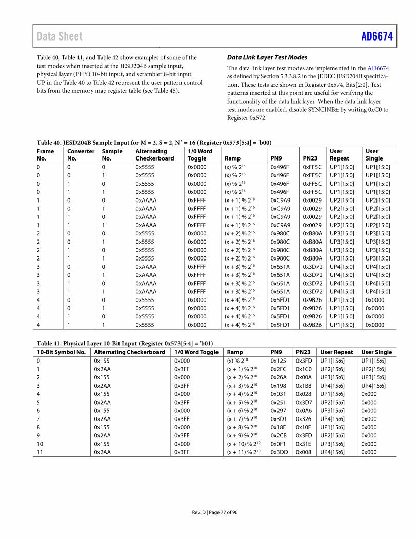
Data Sheet AD6674
Rev. D | Page 77 of 96
Table 40, Table 41, and Table 42 show examples of some of the test modes when inserted at the JESD204B sample input, physical layer (PHY) 10-bit input, and scrambler 8-bit input. UP in the Table 40 to Table 42 represent the user pattern control bits from the memory map register table (see Table 45).
Data Link Layer Test Modes
The data link layer test modes are implemented in the AD6674 as defined by Section 5.3.3.8.2 in the JEDEC JESD204B specifica-tion. These tests are shown in Register 0x574, Bits[2:0]. Test patterns inserted at this point are useful for verifying the functionality of the data link layer. When the data link layer test modes are enabled, disable SYNCINB± by writing 0xC0 to Register 0x572.
Table 40. JESD204B Sample Input for M = 2, S = 2, N΄ = 16 (Register 0x573[5:4] = 'b00) Frame No.
Converter No.
Sample No.
Alternating Checkerboard
1/0 Word Toggle Ramp PN9 PN23
User Repeat
User Single
0 0 0 0x5555 0x0000 (x) % 216 0x496F 0xFF5C UP1[15:0] UP1[15:0] 0 0 1 0x5555 0x0000 (x) % 216 0x496F 0xFF5C UP1[15:0] UP1[15:0] 0 1 0 0x5555 0x0000 (x) % 216 0x496F 0xFF5C UP1[15:0] UP1[15:0] 0 1 1 0x5555 0x0000 (x) % 216 0x496F 0xFF5C UP1[15:0] UP1[15:0] 1 0 0 0xAAAA 0xFFFF (x + 1) % 216 0xC9A9 0x0029 UP2[15:0] UP2[15:0] 1 0 1 0xAAAA 0xFFFF (x + 1) % 216 0xC9A9 0x0029 UP2[15:0] UP2[15:0] 1 1 0 0xAAAA 0xFFFF (x + 1) % 216 0xC9A9 0x0029 UP2[15:0] UP2[15:0] 1 1 1 0xAAAA 0xFFFF (x + 1) % 216 0xC9A9 0x0029 UP2[15:0] UP2[15:0] 2 0 0 0x5555 0x0000 (x + 2) % 216 0x980C 0xB80A UP3[15:0] UP3[15:0] 2 0 1 0x5555 0x0000 (x + 2) % 216 0x980C 0xB80A UP3[15:0] UP3[15:0] 2 1 0 0x5555 0x0000 (x + 2) % 216 0x980C 0xB80A UP3[15:0] UP3[15:0] 2 1 1 0x5555 0x0000 (x + 2) % 216 0x980C 0xB80A UP3[15:0] UP3[15:0] 3 0 0 0xAAAA 0xFFFF (x + 3) % 216 0x651A 0x3D72 UP4[15:0] UP4[15:0] 3 0 1 0xAAAA 0xFFFF (x + 3) % 216 0x651A 0x3D72 UP4[15:0] UP4[15:0] 3 1 0 0xAAAA 0xFFFF (x + 3) % 216 0x651A 0x3D72 UP4[15:0] UP4[15:0] 3 1 1 0xAAAA 0xFFFF (x + 3) % 216 0x651A 0x3D72 UP4[15:0] UP4[15:0] 4 0 0 0x5555 0x0000 (x + 4) % 216 0x5FD1 0x9B26 UP1[15:0] 0x0000 4 0 1 0x5555 0x0000 (x + 4) % 216 0x5FD1 0x9B26 UP1[15:0] 0x0000 4 1 0 0x5555 0x0000 (x + 4) % 216 0x5FD1 0x9B26 UP1[15:0] 0x0000 4 1 1 0x5555 0x0000 (x + 4) % 216 0x5FD1 0x9B26 UP1[15:0] 0x0000
Table 41. Physical Layer 10-Bit Input (Register 0x573[5:4] = 'b01) 10-Bit Symbol No. Alternating Checkerboard 1/0 Word Toggle Ramp PN9 PN23 User Repeat User Single 0 0x155 0x000 (x) % 210 0x125 0x3FD UP1[15:6] UP1[15:6] 1 0x2AA 0x3FF (x + 1) % 210 0x2FC 0x1C0 UP2[15:6] UP2[15:6] 2 0x155 0x000 (x + 2) % 210 0x26A 0x00A UP3[15:6] UP3[15:6] 3 0x2AA 0x3FF (x + 3) % 210 0x198 0x1B8 UP4[15:6] UP4[15:6] 4 0x155 0x000 (x + 4) % 210 0x031 0x028 UP1[15:6] 0x000 5 0x2AA 0x3FF (x + 5) % 210 0x251 0x3D7 UP2[15:6] 0x000 6 0x155 0x000 (x + 6) % 210 0x297 0x0A6 UP3[15:6] 0x000 7 0x2AA 0x3FF (x + 7) % 210 0x3D1 0x326 UP4[15:6] 0x000 8 0x155 0x000 (x + 8) % 210 0x18E 0x10F UP1[15:6] 0x000 9 0x2AA 0x3FF (x + 9) % 210 0x2CB 0x3FD UP2[15:6] 0x000 10 0x155 0x000 (x + 10) % 210 0x0F1 0x31E UP3[15:6] 0x000 11 0x2AA 0x3FF (x + 11) % 210 0x3DD 0x008 UP4[15:6] 0x000
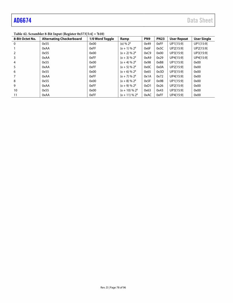
AD6674 Data Sheet
Rev. D | Page 78 of 96
Table 42. Scrambler 8-Bit Input (Register 0x573[5:4] = 'b10) 8-Bit Octet No. Alternating Checkerboard 1/0 Word Toggle Ramp PN9 PN23 User Repeat User Single 0 0x55 0x00 (x) % 28 0x49 0xFF UP1[15:9] UP1[15:9] 1 0xAA 0xFF (x + 1) % 28 0x6F 0x5C UP2[15:9] UP2[15:9] 2 0x55 0x00 (x + 2) % 28 0xC9 0x00 UP3[15:9] UP3[15:9] 3 0xAA 0xFF (x + 3) % 28 0xA9 0x29 UP4[15:9] UP4[15:9] 4 0x55 0x00 (x + 4) % 28 0x98 0xB8 UP1[15:9] 0x00 5 0xAA 0xFF (x + 5) % 28 0x0C 0x0A UP2[15:9] 0x00 6 0x55 0x00 (x + 6) % 28 0x65 0x3D UP3[15:9] 0x00 7 0xAA 0xFF (x + 7) % 28 0x1A 0x72 UP4[15:9] 0x00 8 0x55 0x00 (x + 8) % 28 0x5F 0x9B UP1[15:9] 0x00 9 0xAA 0xFF (x + 9) % 28 0xD1 0x26 UP2[15:9] 0x00 10 0x55 0x00 (x + 10) % 28 0x63 0x43 UP3[15:9] 0x00 11 0xAA 0xFF (x + 11) % 28 0xAC 0xFF UP4[15:9] 0x00
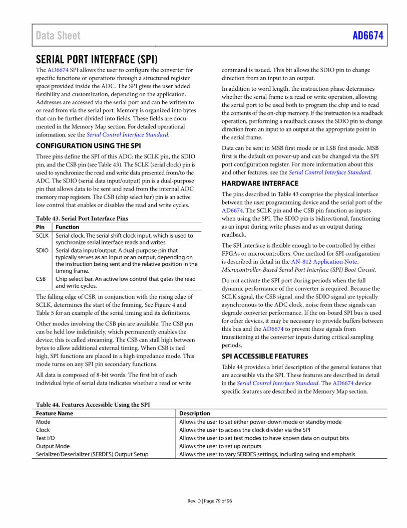
Data Sheet AD6674
Rev. D | Page 79 of 96
SERIAL PORT INTERFACE (SPI) The AD6674 SPI allows the user to configure the converter for specific functions or operations through a structured register space provided inside the ADC. The SPI gives the user added flexibility and customization, depending on the application. Addresses are accessed via the serial port and can be written to or read from via the serial port. Memory is organized into bytes that can be further divided into fields. These fields are docu-mented in the Memory Map section. For detailed operational information, see the Serial Control Interface Standard.
CONFIGURATION USING THE SPI Three pins define the SPI of this ADC: the SCLK pin, the SDIO pin, and the CSB pin (see Table 43). The SCLK (serial clock) pin is used to synchronize the read and write data presented from/to the ADC. The SDIO (serial data input/output) pin is a dual-purpose pin that allows data to be sent and read from the internal ADC memory map registers. The CSB (chip select bar) pin is an active low control that enables or disables the read and write cycles.
Table 43. Serial Port Interface Pins Pin Function SCLK Serial clock. The serial shift clock input, which is used to
synchronize serial interface reads and writes. SDIO Serial data input/output. A dual-purpose pin that
typically serves as an input or an output, depending on the instruction being sent and the relative position in the timing frame.
CSB Chip select bar. An active low control that gates the read and write cycles.
The falling edge of CSB, in conjunction with the rising edge of SCLK, determines the start of the framing. See Figure 4 and Table 5 for an example of the serial timing and its definitions.
Other modes involving the CSB pin are available. The CSB pin can be held low indefinitely, which permanently enables the device; this is called streaming. The CSB can stall high between bytes to allow additional external timing. When CSB is tied high, SPI functions are placed in a high impedance mode. This mode turns on any SPI pin secondary functions.
All data is composed of 8-bit words. The first bit of each individual byte of serial data indicates whether a read or write
command is issued. This bit allows the SDIO pin to change direction from an input to an output.
In addition to word length, the instruction phase determines whether the serial frame is a read or write operation, allowing the serial port to be used both to program the chip and to read the contents of the on-chip memory. If the instruction is a readback operation, performing a readback causes the SDIO pin to change direction from an input to an output at the appropriate point in the serial frame.
Data can be sent in MSB first mode or in LSB first mode. MSB first is the default on power-up and can be changed via the SPI port configuration register. For more information about this and other features, see the Serial Control Interface Standard.
HARDWARE INTERFACE The pins described in Table 43 comprise the physical interface between the user programming device and the serial port of the AD6674. The SCLK pin and the CSB pin function as inputs when using the SPI. The SDIO pin is bidirectional, functioning as an input during write phases and as an output during readback.
The SPI interface is flexible enough to be controlled by either FPGAs or microcontrollers. One method for SPI configuration is described in detail in the AN-812 Application Note, Microcontroller-Based Serial Port Interface (SPI) Boot Circuit.
Do not activate the SPI port during periods when the full dynamic performance of the converter is required. Because the SCLK signal, the CSB signal, and the SDIO signal are typically asynchronous to the ADC clock, noise from these signals can degrade converter performance. If the on-board SPI bus is used for other devices, it may be necessary to provide buffers between this bus and the AD6674 to prevent these signals from transitioning at the converter inputs during critical sampling periods.
SPI ACCESSIBLE FEATURES Table 44 provides a brief description of the general features that are accessible via the SPI. These features are described in detail in the Serial Control Interface Standard. The AD6674 device specific features are described in the Memory Map section.
Table 44. Features Accessible Using the SPI Feature Name Description Mode Allows the user to set either power-down mode or standby mode Clock Allows the user to access the clock divider via the SPI Test I/O Allows the user to set test modes to have known data on output bits Output Mode Allows the user to set up outputs Serializer/Deserializer (SERDES) Output Setup Allows the user to vary SERDES settings, including swing and emphasis
AD6674 Data Sheet
Rev. D | Page 80 of 96
MEMORY MAP READING THE MEMORY MAP REGISTER TABLE Each row in the memory map register table has eight bit locations. The memory map is roughly divided into seven sections: the Analog Devices SPI registers, the analog input buffer control registers, ADC function registers, the DDC function registers, NSR decimate by 2 and noise shaping requantizer registers, variable dynamic range registers, and the digital outputs and test modes registers.
Table 45 (see the Memory Map Register Table section) documents the default hexadecimal value for each hexadecimal address shown. The column with the heading Bit 7 (MSB) is the start of the default hexadecimal value given. For example, Address 0x561, the output mode register, has a hexadecimal default value of 0x01. This means that Bit 0 = 1, and the remaining bits are 0s. This setting is the default output format value, which is twos complement. For more information on this function and others, see the Table 45.
Open and Reserved Locations
All address and bit locations that are not included in Table 45 are not currently supported for this device. Write unused bits of a valid address location with 0s unless the default value is set otherwise. Writing to these locations is required only when part of an address location is open (for example, Address 0x561). If the entire address location is open (for example, Address 0x013), do not write to this address location.
Default Values
After the AD6674 is reset, critical registers are loaded with default values. The default values for the registers are given in the memory map register table, Table 45.
Logic Levels
An explanation of logic level terminology follows:
• “Bit is set” is synonymous with “bit is set to Logic 1” or “writing Logic 1 for the bit.”
• “Clear a bit” is synonymous with “bit is set to Logic 0” or “writing Logic 0 for the bit.”
• “X” denotes a “don’t care”.
Channel Specific Registers
Some channel setup functions such as buffer input termination (Register 0x016) can be programmed to a different value for each channel. In these cases, channel address locations are internally duplicated for each channel. These registers and bits are designated in Table 45 as local. These local registers and bits can be accessed by setting the appropriate Channel A or Channel B bits in Register 0x008. If both bits are set, the subsequent write affects the registers of both channels. In a read cycle, set only Channel A or Channel B to read one of the two registers. If both bits are set during an SPI read cycle, the device returns the value for Channel A. Registers and bits designated as global in Table 45 affect the entire device and the channel features for which independent settings are not allowed between channels. The settings in Register 0x008 do not affect the global registers and bits.
SPI Soft Reset
After issuing a soft reset by programming 0x81 to Register 0x000, the AD6674 requires 5 ms to recover. Therefore, when program-ming the AD6674 for application setup, ensure that an adequate delay is programmed into the firmware after asserting the soft reset and before starting the device setup.
Datapath Soft Reset
After programming the desired settings to the SPI registers, issue a datapath soft reset by programming 0x02 to Register 0x001. This reset function is implemented upon the next rising edge of the input clock, after the register is programmed to issue the datapath soft reset. This reset does not affect the contents of the memory map registers; it only resets the datapath.
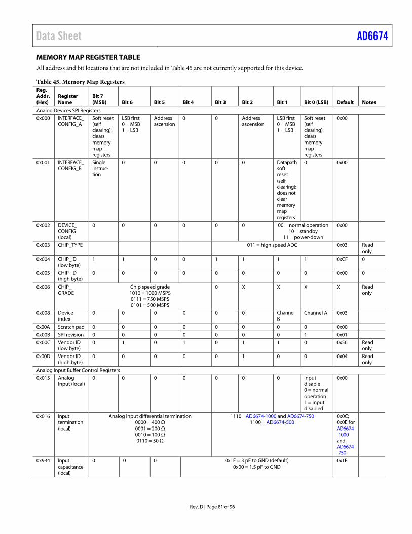
Data Sheet AD6674
Rev. D | Page 81 of 96
MEMORY MAP REGISTER TABLE All address and bit locations that are not included in Table 45 are not currently supported for this device.
Table 45. Memory Map Registers Reg. Addr.(Hex)
Register Name
Bit 7 (MSB) Bit 6 Bit 5 Bit 4 Bit 3 Bit 2 Bit 1 Bit 0 (LSB) Default Notes
Analog Devices SPI Registers
0x000 INTERFACE_CONFIG_A
Soft reset (self clearing): clears memory map registers
LSB first 0 = MSB 1 = LSB
Address ascension
0 0 Address ascension
LSB first 0 = MSB 1 = LSB
Soft reset (self clearing): clears memory map registers
0x00
0x001 INTERFACE_CONFIG_B
Single instruc-tion
0 0 0 0 0 Datapath soft reset (self clearing): does not clear memory map registers
0 0x00
0x002 DEVICE_ CONFIG (local)
0 0 0 0 0 0 00 = normal operation 10 = standby
11 = power-down
0x00
0x003 CHIP_TYPE 011 = high speed ADC 0x03 Read only
0x004 CHIP_ID (low byte)
1 1 0 0 1 1 1 1 0xCF 0
0x005 CHIP_ID (high byte)
0 0 0 0 0 0 0 0 0x00 0
0x006 CHIP_ GRADE
Chip speed grade 1010 = 1000 MSPS 0111 = 750 MSPS 0101 = 500 MSPS
0 X X X X Read only
0x008 Device index
0 0 0 0 0 0 Channel B
Channel A 0x03
0x00A Scratch pad 0 0 0 0 0 0 0 0 0x00
0x00B SPI revision 0 0 0 0 0 0 0 1 0x01
0x00C Vendor ID (low byte)
0 1 0 1 0 1 1 0 0x56 Read only
0x00D Vendor ID (high byte)
0 0 0 0 0 1 0 0 0x04 Read only
Analog Input Buffer Control Registers
0x015 Analog Input (local)
0 0 0 0 0 0 0 Input disable 0 = normal operation 1 = input disabled
0x00
0x016 Input termination (local)
Analog input differential termination 0000 = 400 Ω 0001 = 200 Ω 0010 = 100 Ω 0110 = 50 Ω
1110 =AD6674-1000 and AD6674-750 1100 = AD6674-500
0x0C; 0x0E for AD6674-1000 and AD6674-750
0x934 Input capacitance (local)
0 0 0 0x1F = 3 pF to GND (default) 0x00 = 1.5 pF to GND
0x1F
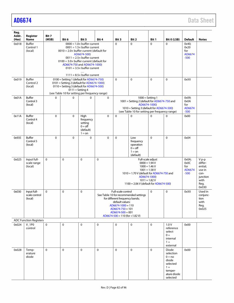
AD6674 Data Sheet
Rev. D | Page 82 of 96
Reg. Addr.(Hex)
Register Name
Bit 7 (MSB) Bit 6 Bit 5 Bit 4 Bit 3 Bit 2 Bit 1 Bit 0 (LSB) Default Notes
0x018 Buffer Control 1 (local)
0000 = 1.0× buffer current 0001 = 1.5× buffer current
0010 = 2.0× buffer current (default for AD6674-500)
0011 = 2.5× buffer current 0100 = 3.0× buffer current (default for
AD6674-750 and AD6674-1000) 0101 = 3.5× buffer current
… 1111 = 8.5× buffer current
0 0 0 0 0x40; 0x20 for AD6674-500
0x019 Buffer Control 2 (local)
0100 = Setting 1 (default for AD6674-750) 0101 = Setting 2 (default for AD6674-1000) 0110 = Setting 3 (default for AD6674-500)
0111 = Setting 4 (see Table 10 for setting per frequency range)
0 0 0 0 0xXX
0x01A Buffer Control 3 (local)
0 0 0 0 1000 = Setting 1 1001 = Setting 2 (default for AD6674-750 and
AD6674-1000) 1010 = Setting 3 (default for AD6674-500)
(see Table 10 for setting per frequency range)
0x09; 0x0A for AD6674-500
0x11A Buffer Control 4 (local)
0 0 High frequency setting 0 = off (default) 1 = on
0 0 0 0 0 0x00
0x935 Buffer Control 5 (local)
0 0 0 0 0 Low frequency operation 0 = off 1 = on (default)
0 0 0x04
0x025 Input full-scale range (local)
0 0 0 0 Full-scale adjust 0000 = 1.94 V 1000 = 1.46 V 1001 = 1.58 V
1010 = 1.70 V (default for AD6674-750 and AD6674-1000) 1011 = 1.82 V
1100 = 2.06 V (default for AD6674-500)
0x0A; 0x0C for AD6674-500
V p-p differ-ential; use in con-junction with Reg. 0x030
0x030 Input full-scale control (local)
0 0 0 Full-scale control See Table 10 for recommended settings
for different frequency bands; default values:
AD6674-1000 = 110 AD6674-750 = 101 AD6674-500 = 001
AD6674-500 = 110 (for <1.82 V)
0 0 0xXX Used in conjunc-tion with Reg. 0x025
ADC Function Registers
0x024 V_1P0 control
0 0 0 0 0 0 0 1.0 V reference select 0 = internal 1 = external
0x00
0x028 Temp-erature diode
0 0 0 0 0 0 0 Diode selection 0 = no diode selected 1 = temper-ature diode selected
0x00
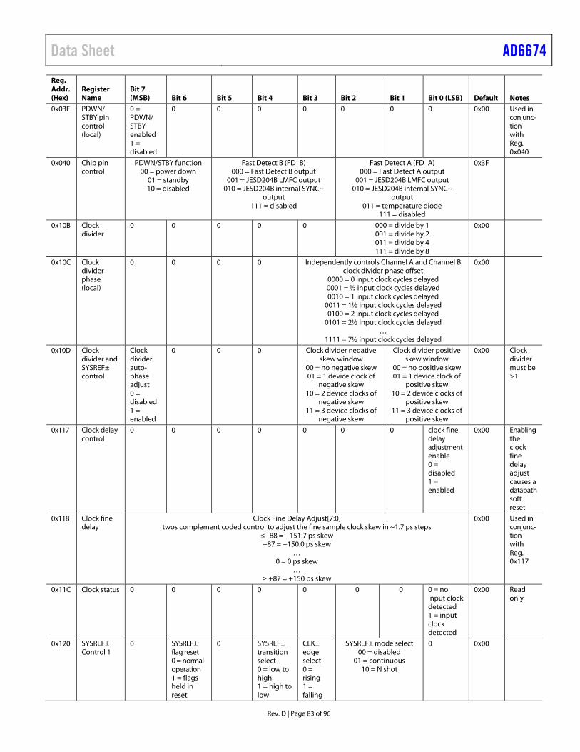
Data Sheet AD6674
Rev. D | Page 83 of 96
Reg. Addr.(Hex)
Register Name
Bit 7 (MSB) Bit 6 Bit 5 Bit 4 Bit 3 Bit 2 Bit 1 Bit 0 (LSB) Default Notes
0x03F PDWN/ STBY pin control (local)
0 = PDWN/ STBY enabled 1 = disabled
0 0 0 0 0 0 0 0x00 Used in conjunc-tion with Reg. 0x040
0x040 Chip pin control
PDWN/STBY function 00 = power down
01 = standby 10 = disabled
Fast Detect B (FD_B) 000 = Fast Detect B output
001 = JESD204B LMFC output 010 = JESD204B internal SYNC~
output 111 = disabled
Fast Detect A (FD_A) 000 = Fast Detect A output
001 = JESD204B LMFC output 010 = JESD204B internal SYNC~
output 011 = temperature diode
111 = disabled
0x3F
0x10B Clock divider
0 0 0 0 0 000 = divide by 1 001 = divide by 2 011 = divide by 4 111 = divide by 8
0x00
0x10C Clock divider phase (local)
0 0 0 0 Independently controls Channel A and Channel B clock divider phase offset
0000 = 0 input clock cycles delayed 0001 = ½ input clock cycles delayed 0010 = 1 input clock cycles delayed
0011 = 1½ input clock cycles delayed 0100 = 2 input clock cycles delayed
0101 = 2½ input clock cycles delayed …
1111 = 7½ input clock cycles delayed
0x00
0x10D Clock divider and SYSREF± control
Clock divider auto- phase adjust 0 = disabled 1 = enabled
0 0 0 Clock divider negative skew window
00 = no negative skew 01 = 1 device clock of
negative skew 10 = 2 device clocks of
negative skew 11 = 3 device clocks of
negative skew
Clock divider positive skew window
00 = no positive skew 01 = 1 device clock of
positive skew 10 = 2 device clocks of
positive skew 11 = 3 device clocks of
positive skew
0x00 Clock divider must be >1
0x117 Clock delay control
0 0 0 0 0 0 0 clock fine delay adjustment enable 0 = disabled 1 = enabled
0x00 Enabling the clock fine delay adjust causes a datapath soft reset
0x118 Clock fine delay
Clock Fine Delay Adjust[7:0] twos complement coded control to adjust the fine sample clock skew in ~1.7 ps steps
≤−88 = −151.7 ps skew −87 = −150.0 ps skew
… 0 = 0 ps skew
… ≥ +87 = +150 ps skew
0x00 Used in conjunc-tion with Reg. 0x117
0x11C Clock status 0 0 0 0 0 0 0 0 = no input clock detected 1 = input clock detected
0x00 Read only
0x120 SYSREF± Control 1
0 SYSREF± flag reset 0 = normal operation 1 = flags held in reset
0 SYSREF± transition select 0 = low to high 1 = high to low
CLK± edge select 0 = rising 1 = falling
SYSREF± mode select 00 = disabled
01 = continuous 10 = N shot
0 0x00
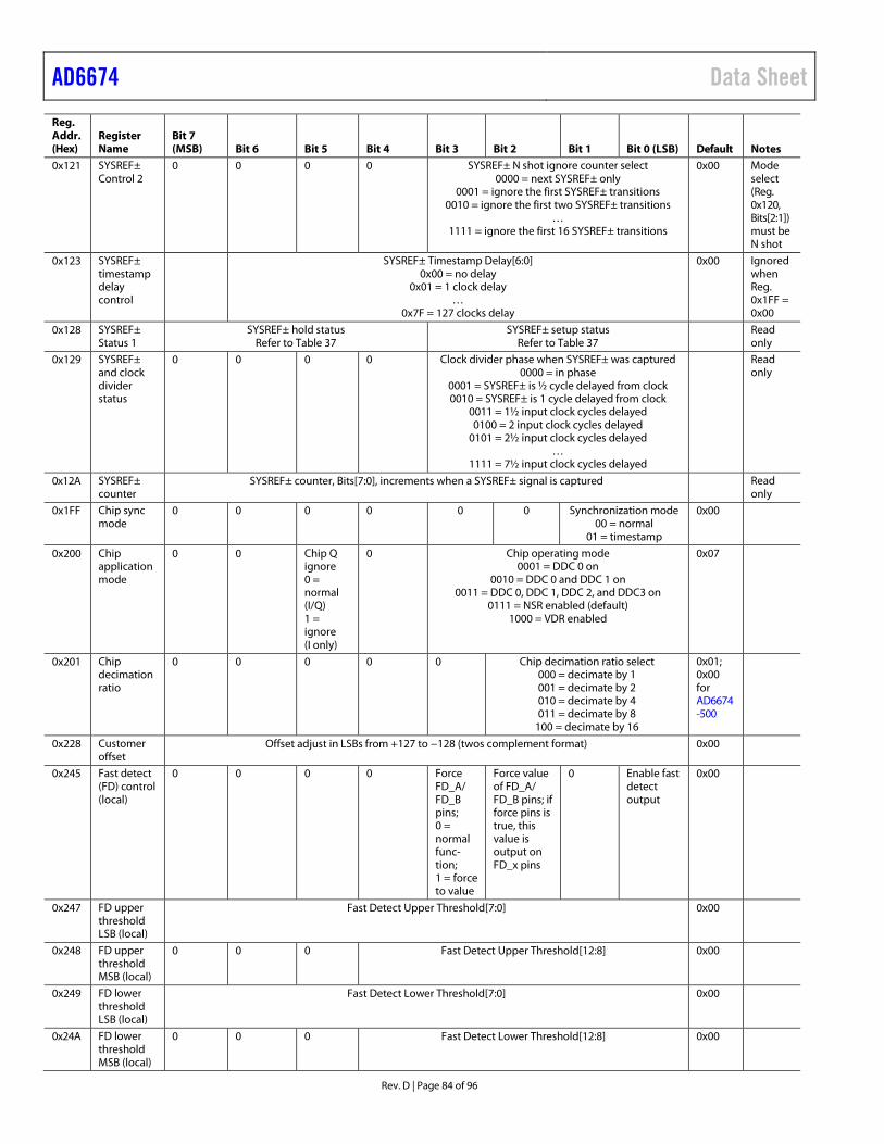
AD6674 Data Sheet
Rev. D | Page 84 of 96
Reg. Addr.(Hex)
Register Name
Bit 7 (MSB) Bit 6 Bit 5 Bit 4 Bit 3 Bit 2 Bit 1 Bit 0 (LSB) Default Notes
0x121 SYSREF± Control 2
0 0 0 0 SYSREF± N shot ignore counter select 0000 = next SYSREF± only
0001 = ignore the first SYSREF± transitions 0010 = ignore the first two SYSREF± transitions
… 1111 = ignore the first 16 SYSREF± transitions
0x00 Mode select (Reg. 0x120, Bits[2:1]) must be N shot
0x123 SYSREF± timestamp delay control
SYSREF± Timestamp Delay[6:0] 0x00 = no delay
0x01 = 1 clock delay …
0x7F = 127 clocks delay
0x00 Ignored when Reg. 0x1FF = 0x00
0x128 SYSREF± Status 1
SYSREF± hold status Refer to Table 37
SYSREF± setup status Refer to Table 37
Read only
0x129 SYSREF± and clock divider status
0 0 0 0 Clock divider phase when SYSREF± was captured 0000 = in phase
0001 = SYSREF± is ½ cycle delayed from clock 0010 = SYSREF± is 1 cycle delayed from clock
0011 = 1½ input clock cycles delayed 0100 = 2 input clock cycles delayed
0101 = 2½ input clock cycles delayed …
1111 = 7½ input clock cycles delayed
Read only
0x12A SYSREF± counter
SYSREF± counter, Bits[7:0], increments when a SYSREF± signal is captured Read only
0x1FF Chip sync mode
0 0 0 0 0 0 Synchronization mode 00 = normal
01 = timestamp
0x00
0x200 Chip application mode
0 0 Chip Q ignore 0 = normal (I/Q) 1 = ignore (I only)
0 Chip operating mode 0001 = DDC 0 on
0010 = DDC 0 and DDC 1 on 0011 = DDC 0, DDC 1, DDC 2, and DDC3 on
0111 = NSR enabled (default) 1000 = VDR enabled
0x07
0x201 Chip decimation ratio
0 0 0 0 0 Chip decimation ratio select 000 = decimate by 1 001 = decimate by 2 010 = decimate by 4 011 = decimate by 8
100 = decimate by 16
0x01; 0x00 for AD6674-500
0x228 Customer offset
Offset adjust in LSBs from +127 to −128 (twos complement format) 0x00
0x245 Fast detect (FD) control (local)
0 0 0 0 Force FD_A/ FD_B pins; 0 = normal func-tion; 1 = force to value
Force value of FD_A/ FD_B pins; if force pins is true, this value is output on FD_x pins
0 Enable fast detect output
0x00
0x247 FD upper threshold LSB (local)
Fast Detect Upper Threshold[7:0] 0x00
0x248 FD upper threshold MSB (local)
0 0 0 Fast Detect Upper Threshold[12:8] 0x00
0x249 FD lower threshold LSB (local)
Fast Detect Lower Threshold[7:0] 0x00
0x24A FD lower threshold MSB (local)
0 0 0 Fast Detect Lower Threshold[12:8] 0x00
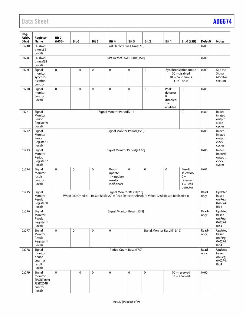
Data Sheet AD6674
Rev. D | Page 85 of 96
Reg. Addr.(Hex)
Register Name
Bit 7 (MSB) Bit 6 Bit 5 Bit 4 Bit 3 Bit 2 Bit 1 Bit 0 (LSB) Default Notes
0x24B FD dwell time LSB (local)
Fast Detect Dwell Time[7:0] 0x00
0x24C FD dwell time MSB (local)
Fast Detect Dwell Time[15:8] 0x00
0x26F Signal monitor synchro-nization control
0 0 0 0 0 0 Synchronization mode 00 = disabled
01 = continuous 11 = 1 shot
0x00 See the Signal Monitor section
0x270 Signal monitor control (local)
0 0 0 0 0 0 Peak detector 0 = disabled 1 = enabled
0 0x00
0x271 Signal Monitor Period Register 0 (local)
Signal Monitor Period[7:1] 0 0x80 In dec-imated output clock cycles
0x272 Signal Monitor Period Register 1 (local)
Signal Monitor Period[15:8] 0x00 In dec-imated output clock cycles
0x273 Signal Monitor Period Register 2 (local)
Signal Monitor Period[23:16] 0x00 In dec-imated output clock cycles
0x274 Signal monitor result control (local)
0 0 0 Result update 1 = update results (self clear)
0 0 0 Result selection 0 = reserved 1 = Peak detector
0x01
0x275 Signal Monitor Result Register 0 (local)
Signal Monitor Result[7:0] When 0x0274[0] = 1, Result Bits[19:7] = Peak Detector Absolute Value[12:0]; Result Bits[6:0] = 0
Read only
Updated based on Reg. 0x0274, Bit 4
0x276 Signal Monitor Result Register 1 (local)
Signal Monitor Result[15:8] Read-only
Updated based on Reg. 0x0274, Bit 4
0x277 Signal Monitor Result Register 1 (local)
0 0 0 0 Signal Monitor Result[19:16] Read-only
Updated based on Reg. 0x0274, Bit 4
0x278 Signal monitor period counter result (local)
Period Count Result[7:0] Read-only
Updated based on Reg. 0x0274, Bit 4
0x279 Signal monitor SPORT over JESD204B control (local)
0 0 0 0 0 0 00 = reserved 11 = enabled
0x00
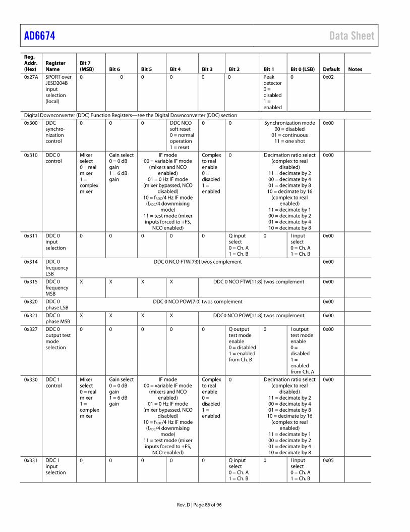
AD6674 Data Sheet
Rev. D | Page 86 of 96
Reg. Addr.(Hex)
Register Name
Bit 7 (MSB) Bit 6 Bit 5 Bit 4 Bit 3 Bit 2 Bit 1 Bit 0 (LSB) Default Notes
0x27A SPORT over JESD204B input selection (local)
0 0 0 0 0 0 Peak detector 0 = disabled 1 = enabled
0 0x02
Digital Downconverter (DDC) Function Registers—see the Digital Downconverter (DDC) section
0x300 DDC synchro-nization control
0 0 0 DDC NCO soft reset 0 = normal operation 1 = reset
0 0 Synchronization mode 00 = disabled
01 = continuous 11 = one shot
0x00
0x310 DDC 0 control
Mixer select 0 = real mixer 1 = complex mixer
Gain select 0 = 0 dB gain 1 = 6 dB gain
IF mode 00 = variable IF mode
(mixers and NCO enabled)
01 = 0 Hz IF mode (mixer bypassed, NCO
disabled) 10 = fADC/4 Hz IF mode
(fADC/4 downmixing mode)
11 = test mode (mixer inputs forced to +FS,
NCO enabled)
Complex to real enable 0 = disabled 1 = enabled
0 Decimation ratio select (complex to real
disabled) 11 = decimate by 2 00 = decimate by 4 01 = decimate by 8
10 = decimate by 16 (complex to real
enabled) 11 = decimate by 1 00 = decimate by 2 01 = decimate by 4 10 = decimate by 8
0x00
0x311 DDC 0 input selection
0 0 0 0 0 Q input select 0 = Ch. A 1 = Ch. B
0 I input select 0 = Ch. A 1 = Ch. B
0x00
0x314 DDC 0 frequency LSB
DDC 0 NCO FTW[7:0] twos complement 0x00
0x315 DDC 0 frequency MSB
X X X X DDC 0 NCO FTW[11:8] twos complement 0x00
0x320 DDC 0 phase LSB
DDC 0 NCO POW[7:0] twos complement 0x00
0x321 DDC 0 phase MSB
X X X X DDC0 NCO POW[11:8] twos complement 0x00
0x327 DDC 0 output test mode selection
0 0 0 0 0 Q output test mode enable 0 = disabled 1 = enabled from Ch. B
0 I output test mode enable 0 = disabled 1 = enabled from Ch. A
0x00
0x330 DDC 1 control
Mixer select 0 = real mixer 1 = complex mixer
Gain select 0 = 0 dB gain 1 = 6 dB gain
IF mode 00 = variable IF mode
(mixers and NCO enabled)
01 = 0 Hz IF mode (mixer bypassed, NCO
disabled) 10 = fADC/4 Hz IF mode
(fADC/4 downmixing mode)
11 = test mode (mixer inputs forced to +FS,
NCO enabled)
Complex to real enable 0 = disabled 1 = enabled
0 Decimation ratio select (complex to real
disabled) 11 = decimate by 2 00 = decimate by 4 01 = decimate by 8
10 = decimate by 16 (complex to real
enabled) 11 = decimate by 1 00 = decimate by 2 01 = decimate by 4 10 = decimate by 8
0x00
0x331 DDC 1 input selection
0 0 0 0 0 Q input select 0 = Ch. A 1 = Ch. B
0 I input select 0 = Ch. A 1 = Ch. B
0x05
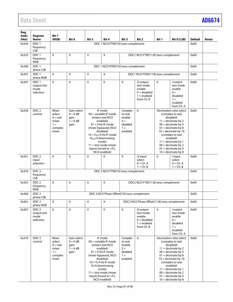
Data Sheet AD6674
Rev. D | Page 87 of 96
Reg. Addr.(Hex)
Register Name
Bit 7 (MSB) Bit 6 Bit 5 Bit 4 Bit 3 Bit 2 Bit 1 Bit 0 (LSB) Default Notes
0x334 DDC 1 frequency LSB
DDC 1 NCO FTW[7:0] twos complement 0x00
0x335 DDC 1 frequency MSB
X X X X DDC1 NCO FTW[11:8] twos complement 0x00
0x340 DDC 1 phase LSB
DDC 1 NCO POW[7:0] twos complement 0x00
0x341 DDC 1 phase MSB
X X X X DDC1 NCO POW[11:8] twos complement 0x00
0x347 DDC 1 output test mode selection
0 0 0 0 0 Q output test mode enable 0 = disabled 1 = enabled from Ch. B
0 I output test mode enable 0 = disabled 1 = enabled from Ch. A
0x00
0x350 DDC 2 control
Mixer select 0 = real mixer 1 = complex mixer
Gain select 0 = 0 dB gain 1 = 6 dB gain
IF mode 00 = variable IF mode
(mixers and NCO enabled)
01 = 0 Hz IF mode (mixer bypassed, NCO
disabled) 10 = fADC/4 Hz IF mode
(fADC/4 downmixing mode)
11 = test mode (mixer inputs forced to +FS,
NCO enabled)
Complex to real enable 0 = disabled 1 = enabled
0 Decimation ratio select (complex to real
disabled) 11 = decimate by 2 00 = decimate by 4 01 = decimate by 8
10 = decimate by 16 (complex to real
enabled) 11 = decimate by 1 00 = decimate by 2 01 = decimate by 4 10 = decimate by 8
0x00
0x351 DDC 2 input selection
0 0 0 0 0 Q input select 0 = Ch. A 1 = Ch. B
0 I input select 0 = Ch. A 1 = Ch. B
0x00
0x354 DDC 2 frequency LSB
DDC 2 NCO FTW[7:0] twos complement 0x00
0x355 DDC 2 frequency MSB
X X X X DDC2 NCO FTW[11:8] twos complement 0x00
0x360 DDC 2 phase LSB
DDC 2 NCO Phase Offset[7:0] twos complement 0x00
0x361 DDC 2 phase MSB
X X X X DDC2 NCO Phase Offset[11:8] twos complement 0x00
0x367 DDC 2 output test mode selection
0 0 0 0 0 Q output test mode enable 0 = disabled 1 = enabled from Ch. B
0 I output test mode enable 0 = disabled 1 = enabled from Ch. A
0x00
0x370 DDC 3 control
Mixer select 0 = real mixer 1 = complex mixer
Gain select 0 = 0 dB gain 1 = 6 dB gain
IF mode 00 = variable IF mode
(mixers and NCO enabled)
01 = 0 Hz IF mode (mixer bypassed, NCO
disabled) 10 = fS/4 Hz IF mode
(fS/4 downmixing mode)
11 = test mode (mixer inputs forced to +FS,
NCO enabled)
Complex to real enable 0 = disabled 1 = enabled
0 Decimation ratio select (complex to real
disabled) 11 = decimate by 2 00 = decimate by 4 01 = decimate by 8
10 = decimate by 16 (complex to real
enabled) 11 = decimate by 1 00 = decimate by 2 01 = decimate by 4 10 = decimate by 8
0x00
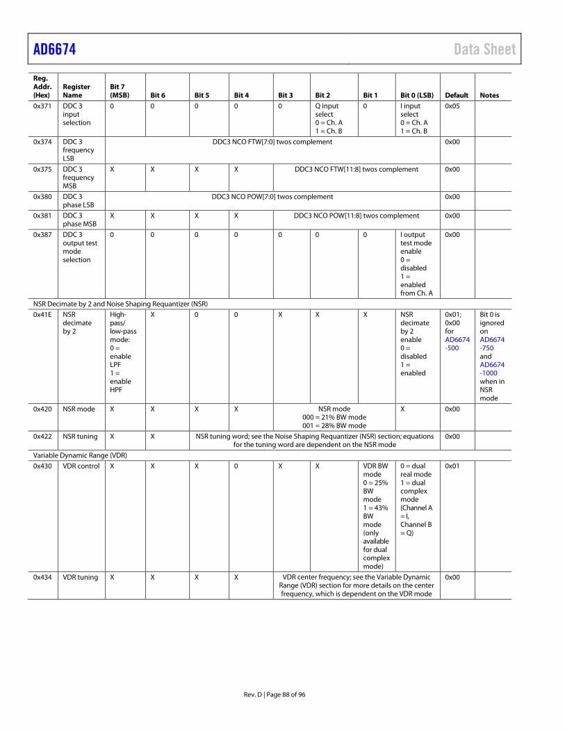
AD6674 Data Sheet
Rev. D | Page 88 of 96
Reg. Addr.(Hex)
Register Name
Bit 7 (MSB) Bit 6 Bit 5 Bit 4 Bit 3 Bit 2 Bit 1 Bit 0 (LSB) Default Notes
0x371 DDC 3 input selection
0 0 0 0 0 Q input select 0 = Ch. A 1 = Ch. B
0 I input select 0 = Ch. A 1 = Ch. B
0x05
0x374 DDC 3 frequency LSB
DDC3 NCO FTW[7:0] twos complement 0x00
0x375 DDC 3 frequency MSB
X X X X DDC3 NCO FTW[11:8] twos complement 0x00
0x380 DDC 3 phase LSB
DDC3 NCO POW[7:0] twos complement 0x00
0x381 DDC 3 phase MSB
X X X X DDC3 NCO POW[11:8] twos complement 0x00
0x387 DDC 3 output test mode selection
0 0 0 0 0 0 0 I output test mode enable 0 = disabled 1 = enabled from Ch. A
0x00
NSR Decimate by 2 and Noise Shaping Requantizer (NSR)
0x41E NSR decimate by 2
High-pass/ low-pass mode: 0 = enable LPF 1 = enable HPF
X 0 0 X X X NSR decimate by 2 enable 0 = disabled 1 = enabled
0x01; 0x00 for AD6674-500
Bit 0 is ignored on AD6674-750 and AD6674-1000 when in NSR mode
0x420 NSR mode X X X X NSR mode 000 = 21% BW mode 001 = 28% BW mode
X 0x00
0x422 NSR tuning X X NSR tuning word; see the Noise Shaping Requantizer (NSR) section; equations for the tuning word are dependent on the NSR mode
0x00
Variable Dynamic Range (VDR)
0x430 VDR control X X X 0 X X VDR BW mode 0 = 25% BW mode 1 = 43% BW mode (only available for dual complex mode)
0 = dual real mode 1 = dual complex mode (Channel A = I, Channel B = Q)
0x01
0x434 VDR tuning X X X X VDR center frequency; see the Variable Dynamic Range (VDR) section for more details on the center frequency, which is dependent on the VDR mode
0x00
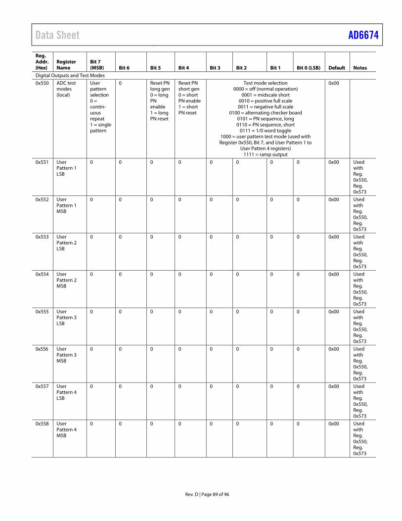
Data Sheet AD6674
Rev. D | Page 89 of 96
Reg. Addr.(Hex)
Register Name
Bit 7 (MSB) Bit 6 Bit 5 Bit 4 Bit 3 Bit 2 Bit 1 Bit 0 (LSB) Default Notes
Digital Outputs and Test Modes
0x550 ADC test modes (local)
User pattern selection 0 = contin-uous repeat 1 = single pattern
0 Reset PN long gen 0 = long PN enable 1 = long PN reset
Reset PN short gen 0 = short PN enable 1 = short PN reset
Test mode selection 0000 = off (normal operation)
0001 = midscale short 0010 = positive full scale 0011 = negative full scale
0100 = alternating checker board 0101 = PN sequence, long 0110 = PN sequence, short
0111 = 1/0 word toggle 1000 = user pattern test mode (used with Register 0x550, Bit 7, and User Pattern 1 to
User Patten 4 registers) 1111 = ramp output
0x00
0x551 User Pattern 1 LSB
0 0 0 0 0 0 0 0 0x00 Used with Reg. 0x550, Reg. 0x573
0x552 User Pattern 1 MSB
0 0 0 0 0 0 0 0 0x00 Used with Reg. 0x550, Reg. 0x573
0x553 User Pattern 2 LSB
0 0 0 0 0 0 0 0 0x00 Used with Reg. 0x550, Reg. 0x573
0x554 User Pattern 2 MSB
0 0 0 0 0 0 0 0 0x00 Used with Reg. 0x550, Reg. 0x573
0x555 User Pattern 3 LSB
0 0 0 0 0 0 0 0 0x00 Used with Reg. 0x550, Reg. 0x573
0x556 User Pattern 3 MSB
0 0 0 0 0 0 0 0 0x00 Used with Reg. 0x550, Reg. 0x573
0x557 User Pattern 4 LSB
0 0 0 0 0 0 0 0 0x00 Used with Reg. 0x550, Reg. 0x573
0x558 User Pattern 4 MSB
0 0 0 0 0 0 0 0 0x00 Used with Reg. 0x550, Reg. 0x573
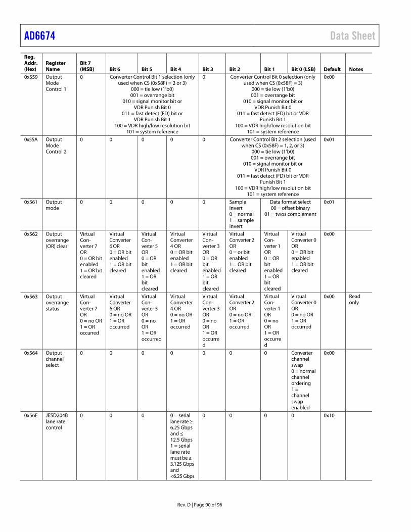
AD6674 Data Sheet
Rev. D | Page 90 of 96
Reg. Addr.(Hex)
Register Name
Bit 7 (MSB) Bit 6 Bit 5 Bit 4 Bit 3 Bit 2 Bit 1 Bit 0 (LSB) Default Notes
0x559 Output Mode Control 1
0 Converter Control Bit 1 selection (only used when CS (0x58F) = 2 or 3)
000 = tie low (1’b0) 001 = overrange bit
010 = signal monitor bit or VDR Punish Bit 0
011 = fast detect (FD) bit or VDR Punish Bit 1
100 = VDR high/low resolution bit 101 = system reference
0 Converter Control Bit 0 selection (only used when CS (0x58F) = 3)
000 = tie low (1’b0) 001 = overrange bit
010 = signal monitor bit or VDR Punish Bit 0
011 = fast detect (FD) bit or VDR Punish Bit 1
100 = VDR high/low resolution bit 101 = system reference
0x00
0x55A Output Mode Control 2
0 0 0 0 0 Converter Control Bit 2 selection (used when CS (0x58F) = 1, 2, or 3)
000 = tie low (1’b0) 001 = overrange bit
010 = signal monitor bit or VDR Punish Bit 0
011 = fast detect (FD) bit or VDR Punish Bit 1
100 = VDR high/low resolution bit 101 = system reference
0x01
0x561 Output mode
0 0 0 0 0 Sample invert 0 = normal 1 = sample invert
Data format select 00 = offset binary
01 = twos complement
0x01
0x562 Output overrange (OR) clear
Virtual Con-verter 7 OR 0 = OR bit enabled 1 = OR bit cleared
Virtual Converter 6 OR 0 = OR bit enabled 1 = OR bit cleared
Virtual Con-verter 5 OR 0 = OR bit enabled 1 = OR bit cleared
Virtual Converter 4 OR 0 = OR bit enabled 1 = OR bit cleared
Virtual Con-verter 3 OR 0 = OR bit enabled 1 = OR bit cleared
Virtual Converter 2 OR 0 = or bit enabled 1 = OR bit cleared
Virtual Con-verter 1 OR 0 = OR bit enabled 1 = OR bit cleared
Virtual Converter 0 OR 0 = OR bit enabled 1 = OR bit cleared
0x00
0x563 Output overrange status
Virtual Con-verter 7 OR 0 = no OR 1 = OR occurred
Virtual Converter 6 OR 0 = no OR 1 = OR occurred
Virtual Con-verter 5 OR 0 = no OR 1 = OR occurred
Virtual Converter 4 OR 0 = no OR 1 = OR occurred
Virtual Con-verter 3 OR 0 = no OR 1 = OR occurred
Virtual Converter 2 OR 0 = no OR 1 = OR occurred
Virtual Con-verter 1 OR 0 = no OR 1 = OR occurred
Virtual Converter 0 OR 0 = no OR 1 = OR occurred
0x00 Read only
0x564 Output channel select
0 0 0 0 0 0 0 Converter channel swap 0 = normal channel ordering 1 = channel swap enabled
0x00
0x56E JESD204B lane rate control
0 0 0 0 = serial lane rate ≥ 6.25 Gbps and ≤ 12.5 Gbps 1 = serial lane rate must be ≥ 3.125 Gbps and <6.25 Gbps
0 0 0 0 0x10
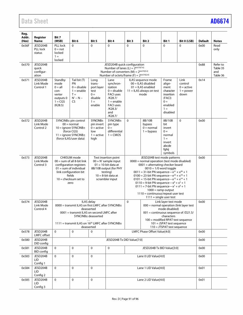
Data Sheet AD6674
Rev. D | Page 91 of 96
Reg. Addr.(Hex)
Register Name
Bit 7 (MSB) Bit 6 Bit 5 Bit 4 Bit 3 Bit 2 Bit 1 Bit 0 (LSB) Default Notes
0x56F JESD204B PLL lock status
PLL lock 0 = not locked 1 = locked
0 0 0 0 0 0 0 0x00 Read only
0x570 JESD204B quick configur-ation
JESD204B quick configuration Number of lanes (L) = 20x570[7:6]
Number of converters (M) = 20x570[5:3] Number of octets/frame (F) = 20x570[2:0]
0x88 Refer to Table 35 and Table 36
0x571 JESD204B Link Mode Control 1
Standby mode 0 = all con-verter outputs 0 1 = CGS (K28.5)
Tail bit (T) PN 0 = disable 1 = enable T = N’ − N − CS
Long trans-port layer test 0 = disable 1 = enable
Lane synchron-ization 0 = disable FACI uses /K28.7/ 1 = enable FACI uses /K28.3/ and /K28.7/
ILAS sequence mode 00 = ILAS disabled 01 = ILAS enabled
11 = ILAS always on test mode
Frame align-ment character insertion (FACI) 0 = enabled 1 = disabled
Link control 0 = active 1 = power down
0x14
0x572 JESD204B Link Mode Control 2
SYNCINB± pin control 00 = normal
10 = ignore SYNCINB± (force CGS)
11 = ignore SYNCINB± (force ILAS/user data)
SYNCINB± pin invert 0 = active low 1 = active high
SYNCINB± pin type 0 = differential 1 = CMOS
0 8B/10B bypass 0 = normal 1 = bypass
8B/10B bit invert 0 = normal 1 = invert abcde fghij symbols
0 0x00
0x573 JESD204B Link Mode Control 3
CHKSUM mode 00 = sum of all 8-bit link configuration registers 01 = sum of individual link configuration bit
fields 10 = checksum set to
zero
Test insertion point 00 = N’ sample input
01 = 10-bit data at 8B/10B output (for PHY
testing) 10 = 8-bit data at scrambler input
JESD204B test mode patterns 0000 = normal operation (test mode disabled)
0001 = alternating checker board 0010 = 1/0 word toggle
0011 = 31-bit PN sequence—x31 + x28 + 1 0100 = 23-bit PN sequence—x23 + x18 + 1 0101 = 15-bit PN sequence—x15 + x14 + 1
0110 = 9-bit PN sequence—x9 + x5 + 1 0111 = 7-bit PN sequence—x7 + x6 + 1
1000 = ramp output 1110 = continuous/repeat user test
1111 = single user test
0x00
0x574 JESD204B Link Mode Control 4
ILAS delay 0000 = transmit ILAS on first LMFC after SYNCINB±
deasserted 0001 = transmit ILAS on second LMFC after
SYNCINB± deasserted …
1111 = transmit ILAS on 16th LMFC after SYNCINB± deasserted
0 Link layer test mode 000 = normal operation (link layer test
mode disabled) 001 = continuous sequence of /D21.5/
characters 100 = modified RPAT test sequence
101 = JSPAT test sequence 110 = JTSPAT test sequence
0x00
0x578 JESD204B LMFC offset
0 0 0 LMFC Phase Offset Value[4:0] 0x00
0x580 JESD204B DID config
JESD204B Tx DID Value[7:0] 0x00
0x581 JESD204B BID config
0 0 0 0 JESD204B Tx BID Value[3:0] 0x00
0x583 JESD204B LID Config 1
0 0 0 Lane 0 LID Value[4:0] 0x00
0x584 JESD204B LID Config 2
0 0 0 Lane 1 LID Value[4:0] 0x01
0x585 JESD204B LID Config 3
0 0 0 Lane 2 LID Value[4:0] 0x01
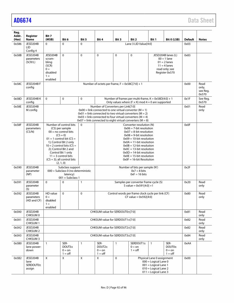
AD6674 Data Sheet
Rev. D | Page 92 of 96
Reg. Addr.(Hex)
Register Name
Bit 7 (MSB) Bit 6 Bit 5 Bit 4 Bit 3 Bit 2 Bit 1 Bit 0 (LSB) Default Notes
0x586 JESD204B LID Config 4
0 0 0 Lane 3 LID Value[4:0] 0x03
0x58B JESD204B parameters (SCR/L)
JESD204B scram-bling (SCR) 0 = disabled 1 = enabled
0 0 0 0 0 JESD204B lanes (L) 00 = 1 lane 01 = 2 lanes 11 = 4 lanes
read only; see Register 0x570
0x83
0x58C JESD204B F config
Number of octets per frame, F = 0x58C[7:0] + 1 0x00 Read only, see Reg. 0x570
0x58D JESD204B K config
0 0 0 Number of frames per multi-frame, K = 0x58D[4:0] + 1 Only values where (F × K) mod 4 = 0 are supported
0x1F See Reg. 0x570
0x58E JESD204B M config
Number of Converters per Link[7:0] 0x00 = link connected to one virtual converter (M = 1) 0x01 = link connected to two virtual converters (M = 2) 0x03 = link connected to four virtual converters (M = 4)
0x07 = link connected to eight virtual converters (M = 8)
0x01 Read only
0x58F JESD204B parameters (CS/N)
Number of control bits (CS) per sample
00 = no control bits (CS = 0)
01 = 1 control bit (CS = 1); Control Bit 2 only
10 = 2 control bits (CS = 2); Control Bit 2 and
Control Bit 1 only 11 = 3 control bits
(CS = 3); all control bits (2, 1, 0)
0 Converter resolution (N) 0x06 = 7-bit resolution 0x07 = 8-bit resolution 0x08 = 9-bit resolution
0x09 = 10-bit resolution 0x0A = 11-bit resolution 0x0B = 12-bit resolution 0x0C = 13-bit resolution 0x0D = 14-bit resolution 0x0E = 15-bit resolution 0x0F = 16-bit Resolution
0x0F
0x590 JESD204B parameter (NP)
Subclass support 000 = Subclass 0 (no deterministic
latency) 001 = Subclass 1
Number of bits per sample (N’) 0x7 = 8 bits
0xF = 16 bits
0x2F
0x591 JESD204B parameter (S)
0 0 1 Samples per converter frame cycle (S) S value = 0x591[4:0] +1
0x20 Read only
0x592 JESD204B parameters (HD and CF)
HD value 0 = disabled 1 = enabled
0 0 Control words per frame clock cycle per link (CF) CF value = 0x592[4:0]
0x80 Read only
0x5A0 JESD204B CHKSUM 0
CHKSUM value for SERDOUT0±[7:0] 0x81 Read only
0x5A1 JESD204B CHKSUM 1
CHKSUM value for SERDOUT1±[7:0] 0x82 Read only
0x5A2 JESD204B CHKSUM 2
CHKSUM value for SERDOUT2±[7:0] 0x82 Read only
0x5A3 JESD204B CHKSUM 3
CHKSUM value for SERDOUT3±[7:0] 0x84 Read only
0x5B0 JESD204B lane power-down
1 SER-DOUT3± 0 = on 1 = off
1 SER-DOUT2± 0 = on 1 = off
1 SERDOUT1± 0 = on 1 = off
1 SER-DOUT0± 0 = on 1 = off
0xAA
0x5B2 JESD204B lane SERDOUT0± assign
X X X X 0 Physical Lane 0 assignment 000 = Logical Lane 0 001 = Logical Lane 1 010 = Logical Lane 2 011 = Logical Lane 3
0x00
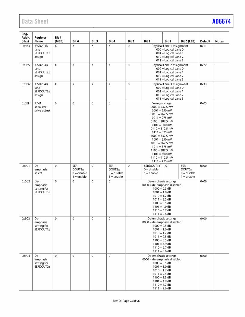
Data Sheet AD6674
Rev. D | Page 93 of 96
Reg. Addr.(Hex)
Register Name
Bit 7 (MSB) Bit 6 Bit 5 Bit 4 Bit 3 Bit 2 Bit 1 Bit 0 (LSB) Default Notes
0x5B3 JESD204B lane SERDOUT1± assign
X X X X 0 Physical Lane 1 assignment 000 = Logical Lane 0 001 = Logical Lane 1 010 = Logical Lane 2 011 = Logical Lane 3
0x11
0x5B5 JESD204B lane SERDOUT2± assign
X X X X 0 Physical Lane 2 assignment 000 = Logical Lane 0 001 = Logical Lane 1 010 = Logical Lane 2 011 = Logical Lane 3
0x22
0x5B6 JESD204B lane SERDOUT3± assign
X X X X 0 Physical Lane 3 assignment 000 = Logical Lane 0 001 = Logical Lane 1 010 = Logical Lane 2 011 = Logical Lane 3
0x33
0x5BF JESD serializer drive adjust
0 0 0 0 Swing voltage 0000 = 237.5 mV 0001 = 250 mV
0010 = 262.5 mV 0011 = 275 mV
0100 = 287.5 mV 0101 = 300 mV
0110 = 312.5 mV 0111 = 325 mV
1000 = 337.5 mV 1001 = 350 mV
1010 = 362.5 mV 1011 = 375 mV
1100 = 387.5 mV 1101 = 400 mV
1110 = 412.5 mV 1111 = 425 mV
0x05
0x5C1 De-emphasis select
0 SER-DOUT3± 0 = disable 1 = enable
0 SER-DOUT2± 0 = disable 1 = enable
0 SERDOUT1± 0 = disable 1 = enable
0 SER-DOUT0± 0 = disable 1 = enable
0x00
0x5C2 De-emphasis setting for SERDOUT0±
0 0 0 0 De-emphasis settings 0000 = de-emphasis disabled
1000 = 0.5 dB 1001 = 1.0 dB 1010 = 1.7 dB 1011 = 2.5 dB 1100 = 3.5 dB 1101 = 4.9 dB 1110 = 6.7 dB 1111 = 9.6 dB
0x00
0x5C3 De-emphasis setting for SERDOUT1±
0 0 0 0 De-emphasis settings 0000 = de-emphasis disabled
1000 = 0.5 dB 1001 = 1.0 dB 1010 = 1.7 dB 1011 = 2.5 dB 1100 = 3.5 dB 1101 = 4.9 dB 1110 = 6.7 dB 1111 = 9.6 dB
0x00
0x5C4 De-emphasis setting for SERDOUT2±
0 0 0 0 De-emphasis settings 0000 = de-emphasis disabled
1000 = 0.5 dB 1001 = 1.0 dB 1010 = 1.7 dB 1011 = 2.5 dB 1100 = 3.5 dB 1101 = 4.9 dB 1110 = 6.7 dB 1111 = 9.6 dB
0x00
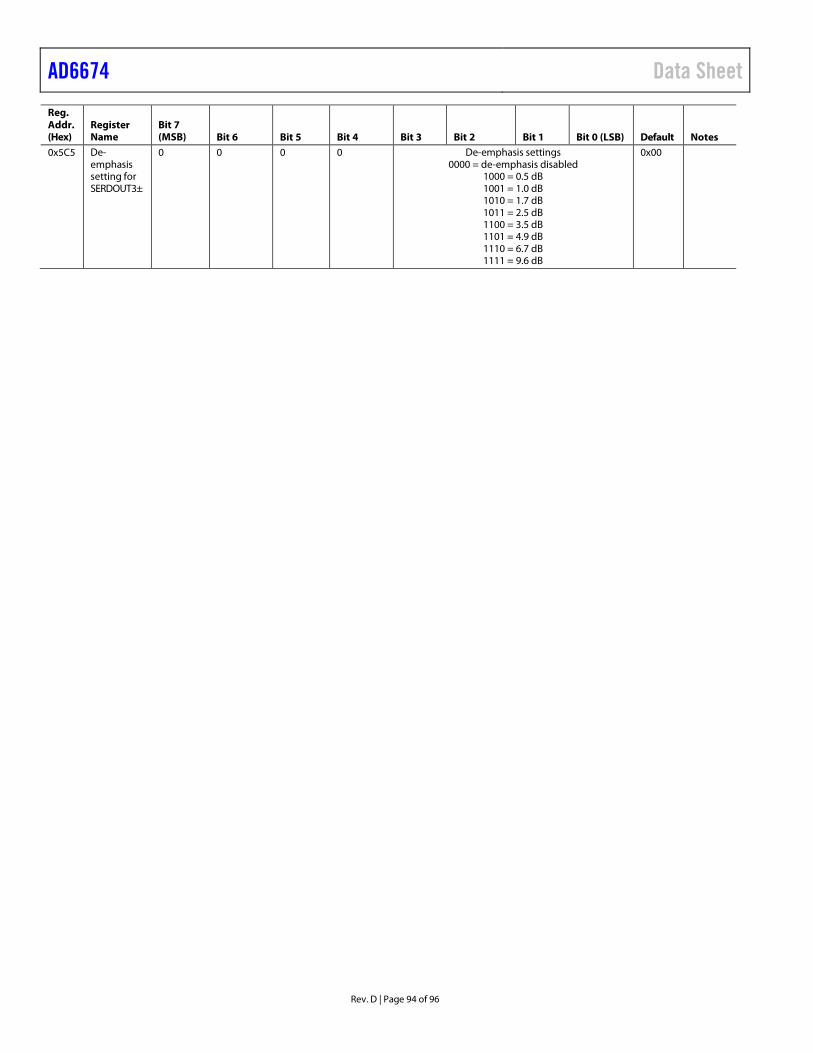
AD6674 Data Sheet
Rev. D | Page 94 of 96
Reg. Addr.(Hex)
Register Name
Bit 7 (MSB) Bit 6 Bit 5 Bit 4 Bit 3 Bit 2 Bit 1 Bit 0 (LSB) Default Notes
0x5C5 De-emphasis setting for SERDOUT3±
0 0 0 0 De-emphasis settings 0000 = de-emphasis disabled
1000 = 0.5 dB 1001 = 1.0 dB 1010 = 1.7 dB 1011 = 2.5 dB 1100 = 3.5 dB 1101 = 4.9 dB 1110 = 6.7 dB 1111 = 9.6 dB
0x00
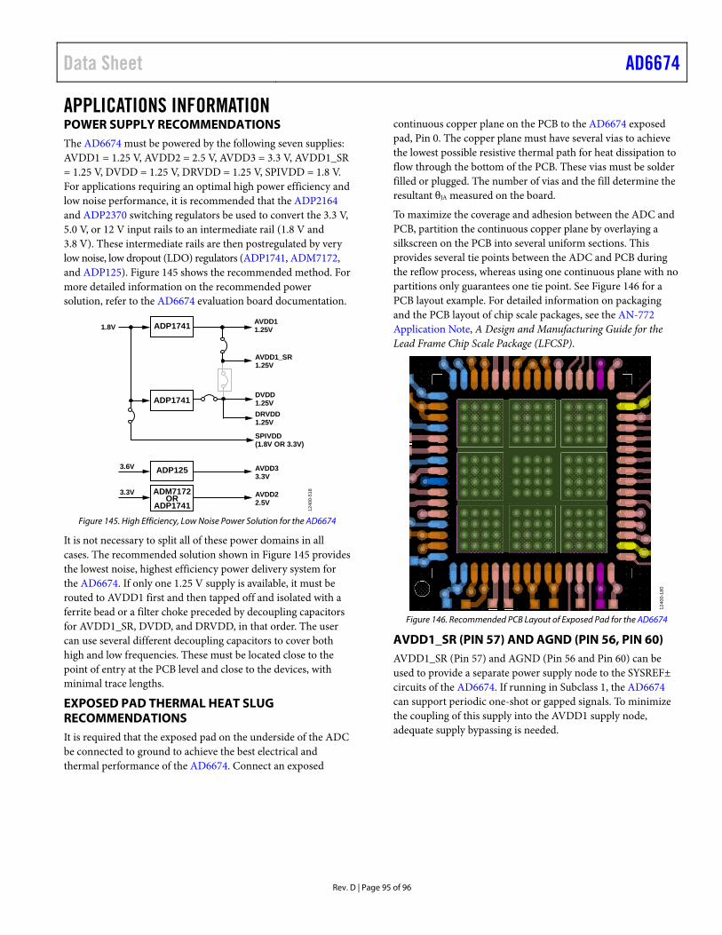
Data Sheet AD6674
Rev. D | Page 95 of 96
APPLICATIONS INFORMATION POWER SUPPLY RECOMMENDATIONS The AD6674 must be powered by the following seven supplies: AVDD1 = 1.25 V, AVDD2 = 2.5 V, AVDD3 = 3.3 V, AVDD1_SR = 1.25 V, DVDD = 1.25 V, DRVDD = 1.25 V, SPIVDD = 1.8 V. For applications requiring an optimal high power efficiency and low noise performance, it is recommended that the ADP2164 and ADP2370 switching regulators be used to convert the 3.3 V, 5.0 V, or 12 V input rails to an intermediate rail (1.8 V and 3.8 V). These intermediate rails are then postregulated by very low noise, low dropout (LDO) regulators (ADP1741, ADM7172, and ADP125). Figure 145 shows the recommended method. For more detailed information on the recommended power solution, refer to the AD6674 evaluation board documentation.
AVDD11.25V
AVDD1_SR1.25V
DVDD1.25V
SPIVDD(1.8V OR 3.3V)
3.6V
3.3V
DRVDD1.25V
1.8V
1240
0-51
8
ADP1741
ADP125 AVDD33.3V
ADM7172OR
ADP1741AVDD22.5V
ADP1741
Figure 145. High Efficiency, Low Noise Power Solution for the AD6674
It is not necessary to split all of these power domains in all cases. The recommended solution shown in Figure 145 provides the lowest noise, highest efficiency power delivery system for the AD6674. If only one 1.25 V supply is available, it must be routed to AVDD1 first and then tapped off and isolated with a ferrite bead or a filter choke preceded by decoupling capacitors for AVDD1_SR, DVDD, and DRVDD, in that order. The user can use several different decoupling capacitors to cover both high and low frequencies. These must be located close to the point of entry at the PCB level and close to the devices, with minimal trace lengths.
EXPOSED PAD THERMAL HEAT SLUG RECOMMENDATIONS It is required that the exposed pad on the underside of the ADC be connected to ground to achieve the best electrical and thermal performance of the AD6674. Connect an exposed
continuous copper plane on the PCB to the AD6674 exposed pad, Pin 0. The copper plane must have several vias to achieve the lowest possible resistive thermal path for heat dissipation to flow through the bottom of the PCB. These vias must be solder filled or plugged. The number of vias and the fill determine the resultant θJA measured on the board.
To maximize the coverage and adhesion between the ADC and PCB, partition the continuous copper plane by overlaying a silkscreen on the PCB into several uniform sections. This provides several tie points between the ADC and PCB during the reflow process, whereas using one continuous plane with no partitions only guarantees one tie point. See Figure 146 for a PCB layout example. For detailed information on packaging and the PCB layout of chip scale packages, see the AN-772 Application Note, A Design and Manufacturing Guide for the Lead Frame Chip Scale Package (LFCSP).
1240
0-18
0
Figure 146. Recommended PCB Layout of Exposed Pad for the AD6674
AVDD1_SR (PIN 57) AND AGND (PIN 56, PIN 60) AVDD1_SR (Pin 57) and AGND (Pin 56 and Pin 60) can be used to provide a separate power supply node to the SYSREF± circuits of the AD6674. If running in Subclass 1, the AD6674 can support periodic one-shot or gapped signals. To minimize the coupling of this supply into the AVDD1 supply node, adequate supply bypassing is needed.
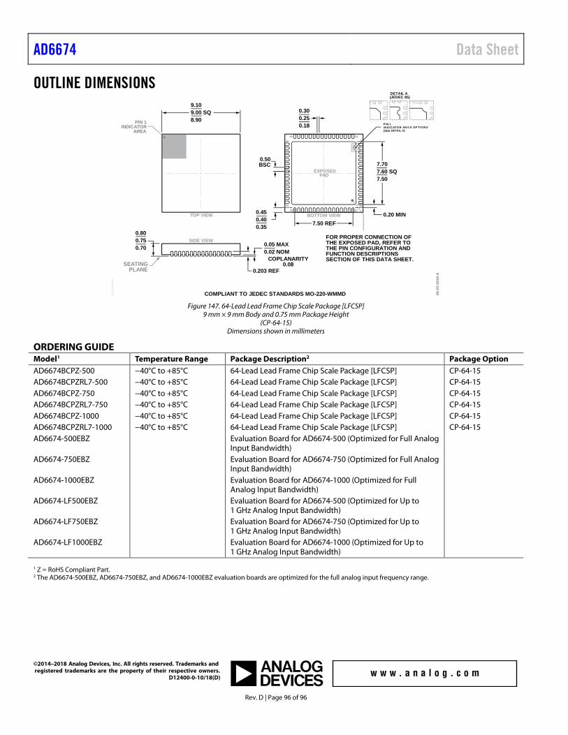
AD6674 Data Sheet
Rev. D | Page 96 of 96
OUTLINE DIMENSIONS
0.50BSC
BOTTOM VIEWTOP VIEW
7.707.60 SQ7.50
0.450.400.35
0.800.750.70 0.05 MAX
0.02 NOM
0.203 REF
COPLANARITY0.08
0.300.250.18
09-2
5-20
18-A
9.109.00 SQ8.90
FOR PROPER CONNECTION OFTHE EXPOSED PAD, REFER TOTHE PIN CONFIGURATION ANDFUNCTION DESCRIPTIONSSECTION OF THIS DATA SHEET.
0.20 MIN7.50 REF
COMPLIANT TO JEDEC STANDARDS MO-220-WMMD
164
1617
49
48
3233
PKG
-004
396
SIDE VIEW
EXPOSEDPAD
SEATINGPLANE
PIN 1INDICATOR
AREA
DETAIL A(JEDEC 95)
PIN 1IN D ICATO R AR E A OP TIO N S(SEE DETAIL A)
Figure 147. 64-Lead Lead Frame Chip Scale Package [LFCSP]
9 mm × 9 mm Body and 0.75 mm Package Height (CP-64-15)
Dimensions shown in millimeters
ORDERING GUIDE Model1 Temperature Range Package Description2 Package Option AD6674BCPZ-500 −40°C to +85°C 64-Lead Lead Frame Chip Scale Package [LFCSP] CP-64-15 AD6674BCPZRL7-500 −40°C to +85°C 64-Lead Lead Frame Chip Scale Package [LFCSP] CP-64-15 AD6674BCPZ-750 −40°C to +85°C 64-Lead Lead Frame Chip Scale Package [LFCSP] CP-64-15 AD6674BCPZRL7-750 −40°C to +85°C 64-Lead Lead Frame Chip Scale Package [LFCSP] CP-64-15 AD6674BCPZ-1000 −40°C to +85°C 64-Lead Lead Frame Chip Scale Package [LFCSP] CP-64-15 AD6674BCPZRL7-1000 −40°C to +85°C 64-Lead Lead Frame Chip Scale Package [LFCSP] CP-64-15 AD6674-500EBZ Evaluation Board for AD6674-500 (Optimized for Full Analog
Input Bandwidth)
AD6674-750EBZ Evaluation Board for AD6674-750 (Optimized for Full Analog Input Bandwidth)
AD6674-1000EBZ Evaluation Board for AD6674-1000 (Optimized for Full Analog Input Bandwidth)
AD6674-LF500EBZ Evaluation Board for AD6674-500 (Optimized for Up to 1 GHz Analog Input Bandwidth)
AD6674-LF750EBZ Evaluation Board for AD6674-750 (Optimized for Up to 1 GHz Analog Input Bandwidth)
AD6674-LF1000EBZ Evaluation Board for AD6674-1000 (Optimized for Up to 1 GHz Analog Input Bandwidth)
1 Z = RoHS Compliant Part. 2 The AD6674-500EBZ, AD6674-750EBZ, and AD6674-1000EBZ evaluation boards are optimized for the full analog input frequency range.
©2014–2018 Analog Devices, Inc. All rights reserved. Trademarks and registered trademarks are the property of their respective owners. D12400-0-10/18(D)


![Test report no. 1307119-2 Ed. 4 - fccid.io€¦ · Antenna UARFCN / Frequency [MHz] No. RF power Channel BW Downlink Uplink Test model 0 1 W (30.0 dBm) 10 MHz 1150/1985.0 18900/1880.0](https://img.pdfslide.net/doc/110x75/5b3747e07f8b9a5a178c0fc4/test-report-no-1307119-2-ed-4-fccidio-antenna-uarfcn-frequency-mhz.jpg)