Embed Size (px)
Citation preview
MICROSTEPPING DMOS DRIVER WITH TRANSLATOR
Always order by complete part number: the prefix ‘A’ + the basic part number(3977) + a suffix letter to indicate operating temperature range + a two-lettersuffix to indicate package style, e.g., A3977SLP .
ABSOLUTE MAXIMUM RATINGS
Load Supply Voltage, VBB ............. 35 VOutput Current, IOUT .................. ±2.5 A*
Logic Supply Voltage, VDD ........... 7.0 VLogic Input Voltage Range, VIN
(tw >30 ns) .... -0.3 V to VDD + 0.3 V(tw <30 ns) .......... -1 V to VDD + 1 V
Sense Voltage, VSENSE ................ 0.5 VReference Voltage, VREF................. VDD
Package Power Dissipation,PD ................................ See page 3
Operating Temperature Range, TA
(A3977Kx)............ -40°C to +125°C(A3977Sx).............. -20°C to +85°C
Junction Temperature, TJ ......... +150°CStorage Temperature Range,
TS ......................... -55°C to +150°C* Output current rating may be limited byduty cycle, ambient temperature, and heatsinking. Under any set of conditions, do notexceed the specified current rating or ajunction temperature of 150°C.
Data S
heet26184.22B
3977
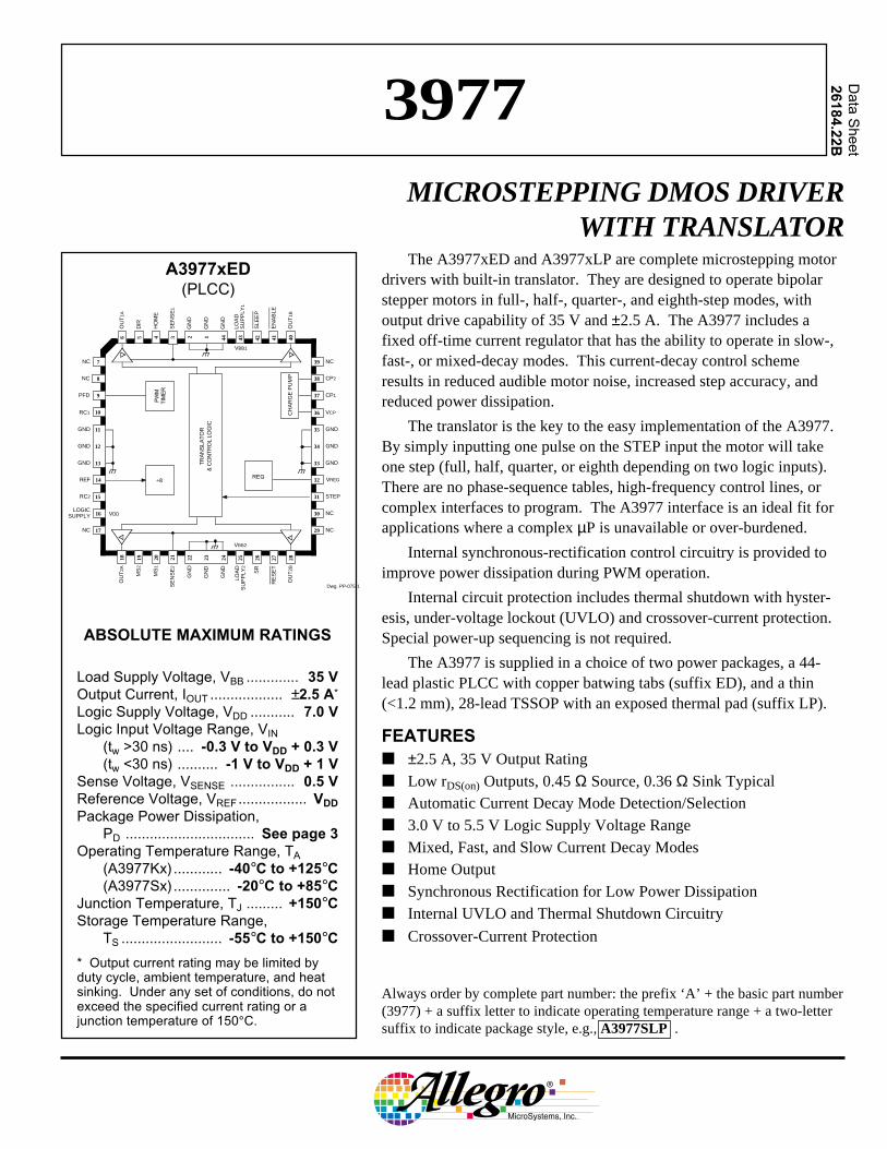
The A3977xED and A3977xLP are complete microstepping motordrivers with built-in translator. They are designed to operate bipolarstepper motors in full-, half-, quarter-, and eighth-step modes, withoutput drive capability of 35 V and ±2.5 A. The A3977 includes afixed off-time current regulator that has the ability to operate in slow-,fast-, or mixed-decay modes. This current-decay control schemeresults in reduced audible motor noise, increased step accuracy, andreduced power dissipation.
The translator is the key to the easy implementation of the A3977.By simply inputting one pulse on the STEP input the motor will takeone step (full, half, quarter, or eighth depending on two logic inputs).There are no phase-sequence tables, high-frequency control lines, orcomplex interfaces to program. The A3977 interface is an ideal fit forapplications where a complex µP is unavailable or over-burdened.
Internal synchronous-rectification control circuitry is provided toimprove power dissipation during PWM operation.
Internal circuit protection includes thermal shutdown with hyster-esis, under-voltage lockout (UVLO) and crossover-current protection.Special power-up sequencing is not required.
The A3977 is supplied in a choice of two power packages, a 44-lead plastic PLCC with copper batwing tabs (suffix ED), and a thin(<1.2 mm), 28-lead TSSOP with an exposed thermal pad (suffix LP).
FEATURES ±2.5 A, 35 V Output Rating Low rDS(on) Outputs, 0.45 Ω Source, 0.36 Ω Sink Typical Automatic Current Decay Mode Detection/Selection 3.0 V to 5.5 V Logic Supply Voltage Range Mixed, Fast, and Slow Current Decay Modes Home Output Synchronous Rectification for Low Power Dissipation Internal UVLO and Thermal Shutdown Circuitry
Crossover-Current Protection
A3977xED(PLCC)
6 5 4 3 2 1 44 43 42 41 40
7
8
9
10
11
12
13
14
15
16
17 29
30
39
38
37
36
35
34
33
32
31
2827262524232221201918
Dwg. PP-075-1
GND
GND
LOGIC SUPPLY
GN
D
GN
D
SE
NS
E1
OU
T1A
NC
GND
GND
REF
RC2
NC
OU
T2A
SE
NS
E2
GN
D
GN
D
GN
D
LOA
D S
UP
PLY
2
OU
T2B
NC
STEP
VREG
GND
GND
VCP
CP1
CP2
NC
OU
T1B
EN
AB
LE
LOA
D
SU
PP
LY1
GN
D
CH
AR
GE
PU
MP
VDD
VBB1
VBB2
NC
MS
2
MS
1
NC
SLE
EP
HO
ME
DIR
PFD
RC1
÷8REG
PW
MT
IME
R
TR
AN
SLA
TO
R&
CO
NTR
OL
LOG
IC
RE
SE
T
SR

115 Northeast Cutoff, Box 15036Worcester, Massachusetts 01615-0036 (508) 853-5000
3977MICROSTEPPING DMOS DRIVERWITH TRANSLATOR
2
Copyright © 2002, 2003 Allegro MicroSystems, Inc.
FUNCTIONAL BLOCK DIAGRAM
DMOS H BRIDGE
DMOS H BRIDGE
GA
TE D
RIV
E
TRA
NS
LATO
R
CHARGEPUMP
CP2 CP1
VCPLOAD
SUPPLY
VBB1
OUT1A
OUT1B
OUT2A
OUT2B
VBB2
SENSE1
VCP
Dwg. FP-050-2
VREG
PWM TIMER
PWM TIMER
PWM LATCHBLANKINGMIXED DECAY
CO
NTR
OL
LOG
IC
UVLO AND
FAULT
REGULATOR
BANDGAP
DAC
+ -
+ -DAC
2 V
SENSE1
PWM LATCHBLANKINGMIXED DECAY
SENSE2
4
4
REF
LOGICSUPPLY
VDD
STEP
DIR
MS1
SLEEP
MS2
HOME
ENABLE
RC1
RESET
SR
PFD
RC2
REF.SUPPLY
VPFD
3977MICROSTEPPING DMOS DRIVER
WITH TRANSLATOR
www.allegromicro.com 3
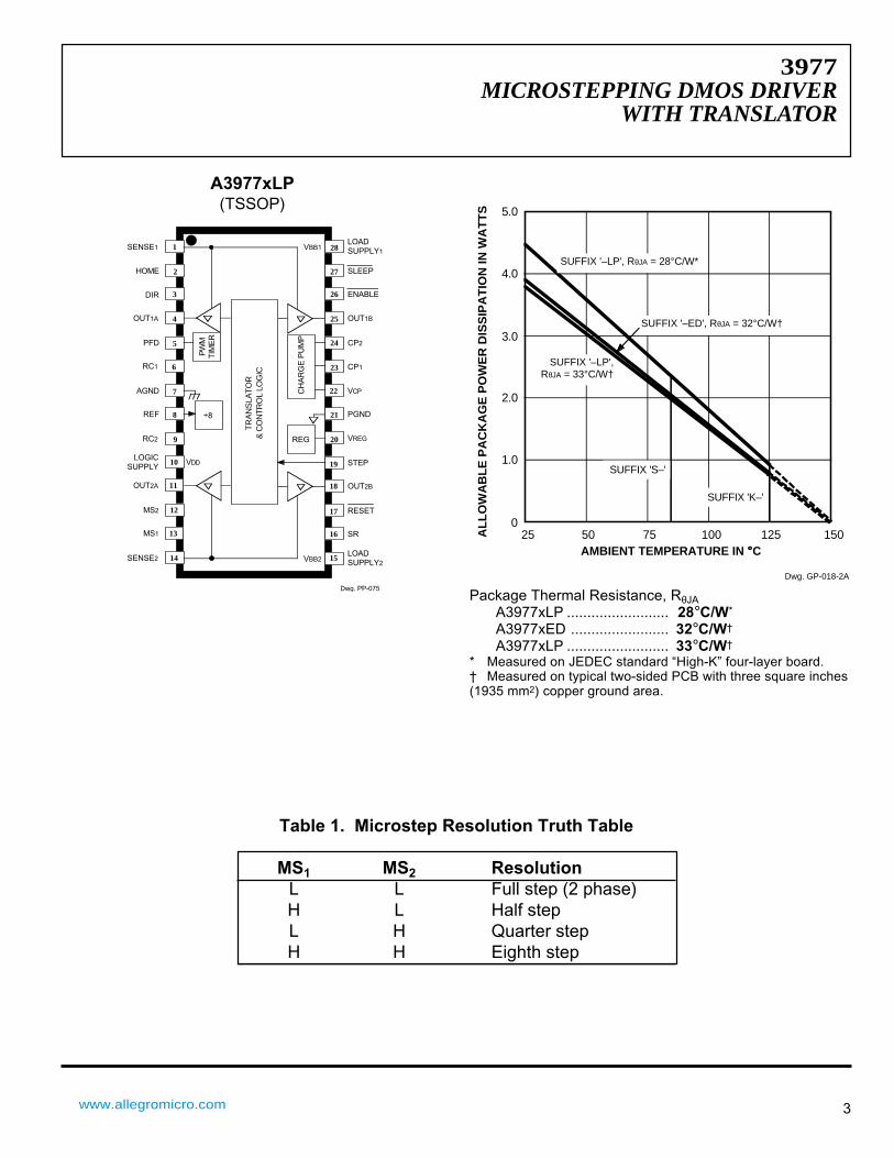
Table 1. Microstep Resolution Truth Table
MS1 MS2 ResolutionL L Full step (2 phase)H L Half stepL H Quarter stepH H Eighth step
A3977xLP(TSSOP)
1
2
3
4
5
6
7
8
9
10
11
12
13
14 15
16
17
18
19
20
21
22
23
24
25
26
27
28LOADSUPPLY1
SLEEP
ENABLE
OUT1B
CP2
CP1
VCP
PGND
VREG
STEP
OUT2B
RESET
SR
LOADSUPPLY2
SENSE1
HOME
DIR
OUT1A
PFD
RC1
AGND
REF
RC2
LOGICSUPPLY
OUT2A
MS2
MS1
SENSE2
÷8
REG
CH
AR
GE
PU
MP
PW
MT
IME
R
TR
AN
SLA
TO
R&
CO
NTR
OL
LOG
IC
VBB2
VBB1
VDD
Dwg. PP-075
Package Thermal Resistance, RθJAA3977xLP ......................... 28°C/W*
A3977xED ........................ 32°C/W†
A3977xLP ......................... 33°C/W†
* Measured on JEDEC standard “High-K” four-layer board.† Measured on typical two-sided PCB with three square inches(1935 mm2) copper ground area.
50 75 100 125 150
5.0
1.0
0
AL
LO
WA
BL
E P
AC
KA
GE
PO
WE
R D
ISS
IPA
TIO
N IN
WA
TT
S
AMBIENT TEMPERATURE IN °°°°C
4.0
3.0
2.0
25
SUFFIX '–LP', RθJA = 33°C/W†
Dwg. GP-018-2A
SUFFIX '–ED', RθJA = 32°C/W†
SUFFIX '–LP', RθJA = 28°C/W*
SUFFIX 'K–'
SUFFIX 'S–'
115 Northeast Cutoff, Box 15036Worcester, Massachusetts 01615-0036 (508) 853-5000
3977MICROSTEPPING DMOS DRIVERWITH TRANSLATOR
4
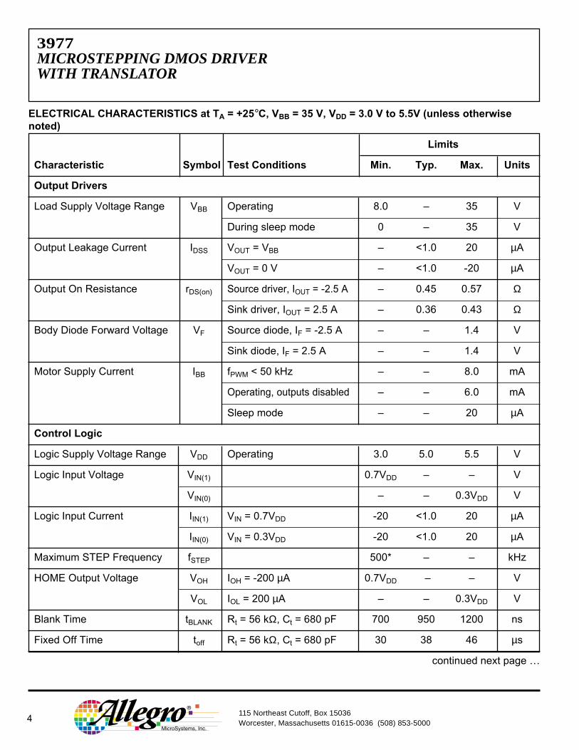
ELECTRICAL CHARACTERISTICS at TA = +25°C, VBB = 35 V, VDD = 3.0 V to 5.5V (unless otherwisenoted)
Limits
Characteristic Symbol Test Conditions Min. Typ. Max. Units
Output Drivers
Load Supply Voltage Range VBB Operating 8.0 – 35 V
During sleep mode 0 – 35 V
Output Leakage Current IDSS VOUT = VBB – <1.0 20 µA
VOUT = 0 V – <1.0 -20 µA
Output On Resistance rDS(on) Source driver, IOUT = -2.5 A – 0.45 0.57 Ω
Sink driver, IOUT = 2.5 A – 0.36 0.43 Ω
Body Diode Forward Voltage VF Source diode, IF = -2.5 A – – 1.4 V
Sink diode, IF = 2.5 A – – 1.4 V
Motor Supply Current IBB fPWM < 50 kHz – – 8.0 mA
Operating, outputs disabled – – 6.0 mA
Sleep mode – – 20 µA
Control Logic
Logic Supply Voltage Range VDD Operating 3.0 5.0 5.5 V
Logic Input Voltage VIN(1) 0.7VDD – – V
VIN(0) – – 0.3VDD V
Logic Input Current IIN(1) VIN = 0.7VDD -20 <1.0 20 µA
IIN(0) VIN = 0.3VDD -20 <1.0 20 µA
Maximum STEP Frequency fSTEP 500* – – kHz
HOME Output Voltage VOH IOH = -200 µA 0.7VDD – – V
VOL IOL = 200 µA – – 0.3VDD V
Blank Time tBLANK Rt = 56 kΩ, Ct = 680 pF 700 950 1200 ns
Fixed Off Time toff Rt = 56 kΩ, Ct = 680 pF 30 38 46 µs
continued next page …
3977MICROSTEPPPING DMOS DRIVER
WITH TRANSLATOR
www.allegromicro.com 5
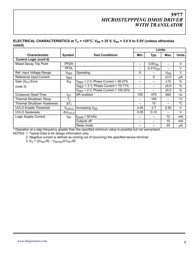
ELECTRICAL CHARACTERISTICS at TA = +25°C, VBB = 35 V, VDD = 3.0 V to 5.5V (unless otherwise noted)
Characteristic Symbol Test ConditionsLimits
Min. Typ. Max. UnitsControl Logic (cont’d)Mixed Decay Trip Point PFDH – 0.6VDD – V
PFDL – 0.21VDD – VRef. Input Voltage Range VREF Operating 0 – VDD VReference Input Current IREF – 0 ±3.0 µAGain (Gm) Error(note 3)
EG VREF = 2 V, Phase Current = 38.27% – – ±10 %VREF = 2 V, Phase Current = 70.71% – – ±5.0 %VREF = 2 V, Phase Current = 100.00% – – ±5.0 %
Crossover Dead Time tDT SR enabled 100 475 800 nsThermal Shutdown Temp. TJ – 165 – °CThermal Shutdown Hysteresis ∆TJ – 15 – °CUVLO Enable Threshold VUVLO Increasing VDD 2.45 2.7 2.95 VUVLO Hysteresis ∆VUVLO 0.05 0.10 – VLogic Supply Current IDD fPWM < 50 kHz – – 12 mA
Outputs off – – 10 mASleep mode – – 20 µA
* Operation at a step frequency greater than the specifi ed minimum value is possible but not warranteed. NOTES: 1. Typical Data is for design information only. 2. Negative current is defi ned as coming out of (sourcing) the specifi ed device terminal. 3. EG = ([VREF/8] – VSENSE)/(VREF/8)

115 Northeast Cutoff, Box 15036Worcester, Massachusetts 01615-0036 (508) 853-5000
3977MICROSTEPPING DMOS DRIVERWITH TRANSLATOR
6
Device Operation. The A3977 is a completemicrostepping motor driver with built in translator foreasy operation with minimal control lines. It is designedto operate bipolar stepper motors in full-, half-, quarter-and eighth-step modes. The current in each of the twooutput H-bridges, all n-channel DMOS, is regulated withfixed off time pulse-width modulated (PWM) controlcircuitry. The H-bridge current at each step is set by thevalue of an external current sense resistor (RS), a referencevoltage (VREF), and the DAC’s output voltage controlledby the output of the translator.
At power up, or reset, the translator sets the DACs andphase current polarity to initial home state (see figures forhome-state conditions), and sets the current regulator forboth phases to mixed-decay mode. When a step commandsignal occurs on the STEP input the translator automati-cally sequences the DACs to the next level (see table 2 forthe current level sequence and current polarity). Themicrostep resolution is set by inputs MS1 and MS2 asshown in table 1. If the new DAC output level is lowerthan the previous level the decay mode for that H-bridgewill be set by the PFD input (fast, slow or mixed decay).If the new DAC level is higher or equal to the previouslevel then the decay mode for that H-bridge will be slowdecay. This automatic current-decay selection willimprove microstepping performance by reducing thedistortion of the current waveform due to the motorBEMF.
Reset Input (RESET). The RESET input (active low)sets the translator to a predefined home state (see figuresfor home state conditions) and turns off all of the DMOSoutputs. The HOME output goes low and all STEP inputsare ignored until the RESET input goes high.
Home Output (HOME). The HOME output is a logicoutput indicator of the initial state of the translator. Atpower up the translator is reset to the home state (seefigures for home state conditions).
Step Input (STEP). A low-to-high transition on theSTEP input sequences the translator and advances themotor one increment. The translator controls the input tothe DACs and the direction of current flow in each wind-ing. The size of the increment is determined by the stateof inputs MS1 and MS2 (see table 1).
Microstep Select (MS1 and MS2). Input terminalsMS1 and MS2 select the microstepping format pertable 1. Changes to these inputs do not take effect untilthe STEP command (see figure).
Direction Input (DIR). The state of the DIRECTIONinput will determine the direction of rotation of the motor.
Internal PWM Current Control. Each H-bridge iscontrolled by a fixed off time PWM current-control circuitthat limits the load current to a desired value (ITRIP).Initially, a diagonal pair of source and sink DMOS outputsare enabled and current flows through the motor windingand RS. When the voltage across the current-sense resistorequals the DAC output voltage, the current-sense com-parator resets the PWM latch, which turns off the sourcedriver (slow-decay mode) or the sink and source drivers(fast- or mixed-decay modes).
The maximum value of current limiting is set by theselection of RS and the voltage at the VREF input with atransconductance function approximated by:
ITRIPmax = VREF/8RS
The DAC output reduces the VREF output to thecurrent-sense comparator in precise steps (see table 2 for% ITRIPmax at each step).
ITRIP = (% ITRIPmax/100) x ITRIPmax
It is critical to ensure that the maximum rating (0.5 V)on the SENSE terminal is not exceeded. For full-stepmode, VREF can be applied up to the maximum rating ofVDD, because the peak sense value is 0.707 x VREF/8. Inall other modes VREF should not exceed 4 V.
Functional Description

3977MICROSTEPPING DMOS DRIVER
WITH TRANSLATOR
www.allegromicro.com 7
Fixed Off-Time. The internal PWM current-controlcircuitry uses a one shot to control the time the driver(s)remain(s) off. The one shot off-time, toff, is determined bythe selection of an external resistor (RT) and capacitor(CT) connected from the RC timing terminal to ground.The off time, over a range of values of CT = 470 pF to1500 pF and RT = 12 kΩ to 100 kΩ is approximated by:
toff = RTCT
RC Blanking. In addition to the fixed off time of thePWM control circuit, the CT component sets the compara-tor blanking time. This function blanks the output of thecurrent-sense comparator when the outputs are switchedby the internal current-control circuitry. The comparatoroutput is blanked to prevent false over-current detectiondue to reverse recovery currents of the clamp diodes, and/or switching transients related to the capacitance of theload. The blank time tBLANK can be approximated by:
tBLANK = 1400CT
Charge Pump. (CP1 and CP2). The charge pump isused to generate a gate supply greater than VBB to drivethe source-side DMOS gates. A 0.22 µF ceramic capaci-tor should be connected between CP1 and CP2 for pump-ing purposes. A 0.22 µF ceramic capacitor is requiredbetween VCP and VBB to act as a reservoir to operate thehigh-side DMOS devices.
VREG. This internally generated voltage is used to operatethe sink-side DMOS outputs. The VREG terminal shouldbe decoupled with a 0.22 µF capacitor to ground. VREG isinternally monitored and in the case of a fault condition,the outputs of the device are disabled.
Enable Input (ENABLE). This active-low inputenables all of the DMOS outputs. When logic high theoutputs are disabled. Inputs to the translator (STEP,DIRECTION, MS1, MS2) are all active independent of theENABLE input state.
Shutdown. In the event of a fault (excessive junctiontemperature, or low voltage on VCP) the outputs of thedevice are disabled until the fault condition is removed.At power up, and in the event of low VDD, the under-voltage lockout (UVLO) circuit disables the drivers andresets the translator to the HOME state.
Sleep Mode (SLEEP). An active-low control inputused to minimize power consumption when not in use.This disables much of the internal circuitry including theoutput DMOS, regulator, and charge pump. A logic highallows normal operation and startup of the device in thehome position. When coming out of sleep mode, wait1 ms before issuing a STEP command to allow the chargepump (gate drive) to stabilize.
Percent Fast Decay Input (PFD). When a STEPinput signal commands a lower output current from theprevious step, it switches the output current decay to eitherslow-, fast-, or mixed-decay depending on the voltagelevel at the PFD input. If the voltage at the PFD input isgreater than 0.6VDD then slow-decay mode is selected. Ifthe voltage on the PFD input is less than 0.21VDD thenfast-decay mode is selected. Mixed decay is betweenthese two levels. This terminal should be decoupled witha 0.1 µF capacitor.
Mixed Decay Operation. If the voltage on the PFDinput is between 0.6VDD and 0.21VDD, the bridge willoperate in mixed-decay mode depending on the stepsequence (see figures). As the trip point is reached, thedevice will go into fast-decay mode until the voltage onthe RC terminal decays to the voltage applied to the PFDterminal. The time that the device operates in fast decay isapproximated by:
tFD = RTCTIn (0.6VDD/VPFD)
After this fast decay portion, tFD, the device willswitch to slow-decay mode for the remainder of the fixedoff-time period.
Functional Description (cont’d)
115 Northeast Cutoff, Box 15036Worcester, Massachusetts 01615-0036 (508) 853-5000
3977MICROSTEPPING DMOS DRIVERWITH TRANSLATOR
8
Synchronous Rectification. When a PWM off cycleis triggered by an internal fixed off-time cycle, loadcurrent will recirculate according to the decay modeselected by the control logic. The A3977 synchronousrectification feature will turn on the appropriateMOSFETs during the current decay and effectively shortout the body diodes with the low rDS(on) driver. This willreduce power dissipation significantly and eliminate theneed for external Schottky diodes for most applications.
The synchronous rectification can be set in eitheractive mode or disabled mode.
Functional Description (cont’d)
Active Mode. When the SR input is logic low, activemode is enabled and synchronous rectification will occur.This mode prevents reversal of the load current by turningoff synchronous rectification when a zero current level isdetected. This prevents the motor winding from conduct-ing in the reverse direction.
Disabled Mode. When the SR input is logic high,synchronous rectification is disabled. This mode istypically used when external diodes are required totransfer power dissipation from the A3977 package to theexternal diodes.
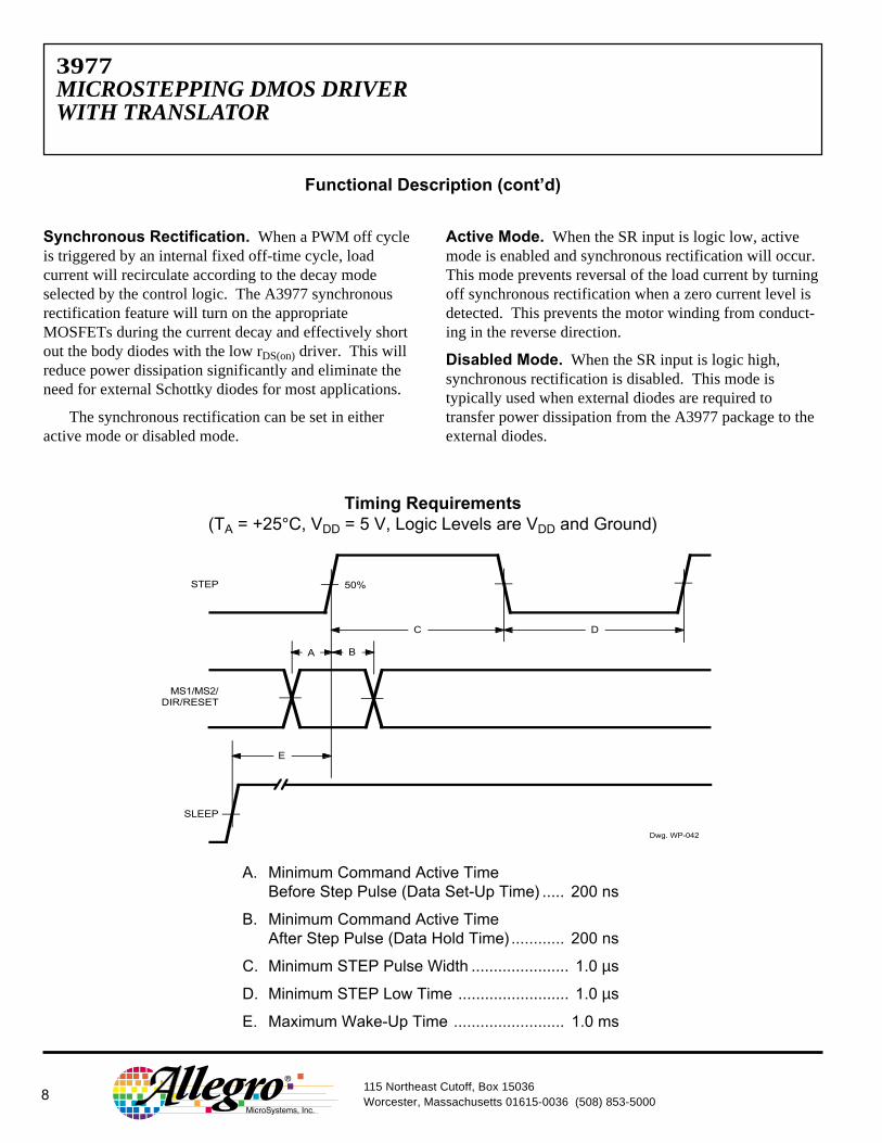
Timing Requirements(TA = +25°C, VDD = 5 V, Logic Levels are VDD and Ground)
A B
C D
50%STEP
MS1/MS2/DIR/RESET
Dwg. WP-042
SLEEP
E
A. Minimum Command Active TimeBefore Step Pulse (Data Set-Up Time) ..... 200 ns
B. Minimum Command Active TimeAfter Step Pulse (Data Hold Time)............ 200 ns
C. Minimum STEP Pulse Width ...................... 1.0 µs
D. Minimum STEP Low Time ......................... 1.0 µs
E. Maximum Wake-Up Time ......................... 1.0 ms
3977MICROSTEPPING DMOS DRIVER
WITH TRANSLATOR
www.allegromicro.com 9
Layout.
The printed wiring board should use a heavy groundplane.
For optimum electrical and thermal performance, thedriver should be soldered directly onto the board.
The load supply terminal, VBB, should be decoupledwith an electrolytic capacitor (>47 µF is recommended)placed as close to the device as possible.
To avoid problems due to capacitive coupling of thehigh dv/dt switching transients, route the bridge-outputtraces away from the sensitive logic-input traces. Alwaysdrive the logic inputs with a low source impedance toincrease noise immunity.
Grounding. A star ground system located close to thedriver is recommended.
The 44-lead PLCC has the analog ground and thepower ground internally bonded to the power tabs of thepackage (leads 44, 1, 2, 11 – 13, 22 – 24, and 33 – 35).
On the 28-lead TSSOP package, the analog ground(lead 7) and the power ground (lead 21) must be con-nected together externally. The copper ground planelocated under the exposed thermal pad is typically used asthe star ground.
Applications Information
Current Sensing. To minimize inaccuracies caused byground-trace IR drops in sensing the output current level,the current-sense resistor (RS) should have an independentground return to the star ground of the device. This pathshould be as short as possible. For low-value senseresistors the IR drops in the printed wiring board senseresistor’s traces can be significant and should be takeninto account. The use of sockets should be avoided asthey can introduce variation in RS due to their contactresistance.
Allegro MicroSystems recommends a value of RS
given by
RS = 0.5/ITRIPmax
Thermal Protection. Circuitry turns off all driverswhen the junction temperature reaches 165°C, typically.It is intended only to protect the device from failures dueto excessive junction temperatures and should not implythat output short circuits are permitted. Thermal shut-down has a hysteresis of approximately 15°C.

3977MICROSTEPPPING DMOS DRIVER WITH TRANSLATOR
115 Northeast Cutoff, Box 15036 Worcester, Massachusetts 01615-0036 (508) 853-500010
Full Step Half Step ¼ Step ⅛ StepPhase 1 Current
(%Itripmax)(%)
Phase 2 Current(%Itripmax)
(%)
Step Angle(º)
1 1 1 100.00 0.00 0.0
2 98.08 19.51 11.3
2 3 92.39 38.27 22.5
4 83.15 55.56 33.8
1 2 3 5 70.71 70.71 45.0
6 55.56 83.15 56.3
4 7 38.27 92.39 67.5
8 19.51 98.08 78.8
3 5 9 0.00 100.00 90.0
10 –19.51 98.08 101.3
6 11 –38.27 92.39 112.5
12 –55.56 83.15 123.8
2 4 7 13 –70.71 70.71 135.0
14 –83.15 55.56 146.3
8 15 –92.39 38.27 157.5
16 –98.08 19.51 168.8
5 9 17 –100.00 0.00 180.0
18 –98.08 –19.51 191.3
10 19 –92.39 –38.27 202.5
20 –83.15 –55.56 213.8
3 6 11 21 –70.71 –70.71 225.0
22 –55.56 –83.15 236.3
12 23 –38.27 –92.39 247.5
24 –19.51 –98.08 258.8
7 13 25 0.00 –100.00 270.0
26 19.51 –98.08 281.3
14 27 38.27 –92.39 292.5
28 55.56 –83.15 303.8
4 8 15 29 70.71 –70.71 315.0
30 83.15 –55.56 326.3
16 31 92.39 –38.27 337.5
32 98.08 –19.51 348.8
Table 2. Step SequencingHome State = 45º Step Angle, DIR = H
3977MICROSTEPPING DMOS DRIVER
WITH TRANSLATOR
www.allegromicro.com 11
Dwg. WK-004-15
PHASE 1CURRENT
PHASE 2CURRENT
SLOWDECAY
STEPINPUT
HOMEOUTPUT
70.7%
–70.7%
70.7%
–70.7%
SLOWDECAY
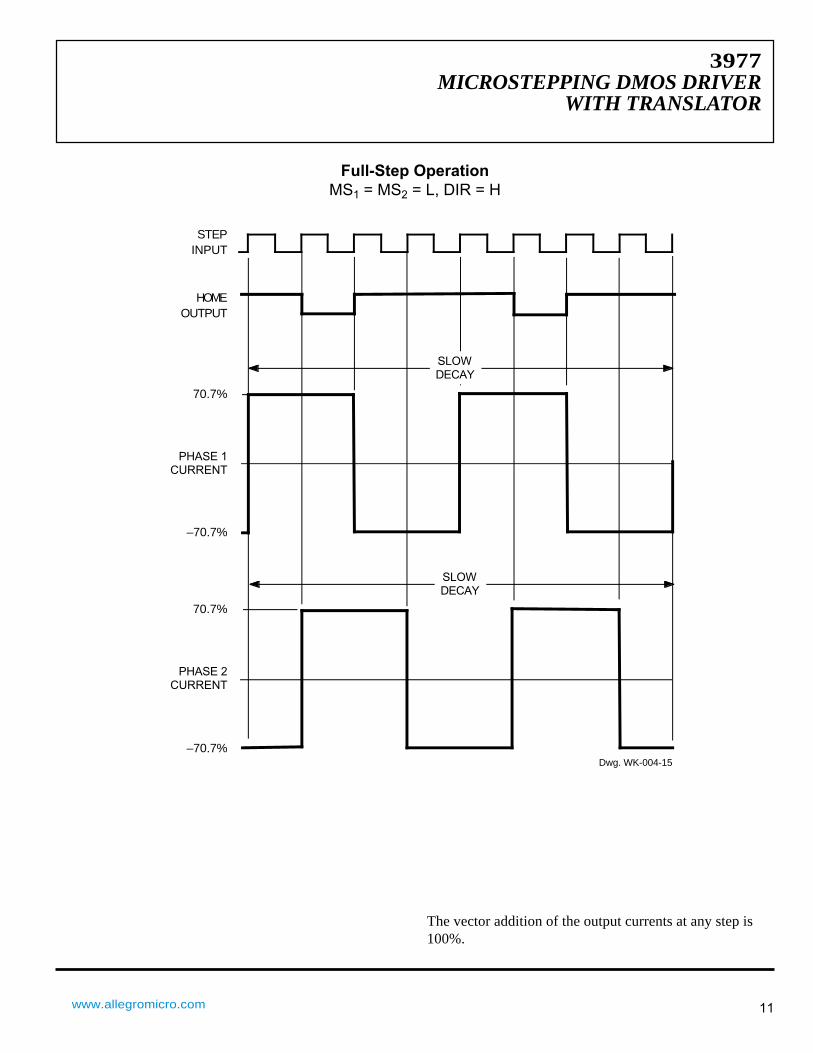
Full-Step OperationMS1 = MS2 = L, DIR = H
The vector addition of the output currents at any step is100%.

115 Northeast Cutoff, Box 15036Worcester, Massachusetts 01615-0036 (508) 853-5000
3977MICROSTEPPING DMOS DRIVERWITH TRANSLATOR
12
Dwg. WK-004-14
PHASE 1CURRENT
PHASE 2CURRENT
SLO
WD
EC
AY
MIX
ED
DE
CA
Y
SLO
WD
EC
AY
MIX
ED
DE
CA
Y
STEPINPUT
HOMEOUTPUT
100%
–100%
100%
–100%
SLO
WD
EC
AY
MIX
ED
DE
CA
Y
SLO
WD
EC
AY
MIX
ED
DE
CA
Y
SLO
WD
EC
AY
MIX
ED
DE
CA
Y
SLO
WD
EC
AY
MIX
ED
DE
CA
Y
SLO
WD
EC
AY
MIX
ED
DE
CA
Y
SLO
WD
EC
AY
MIX
ED
DE
CA
Y
70.7%
–70.7%
70.7%
–70.7%
Half-Step OperationMS1 = H, MS2 = L, DIR = H
The mixed-decay mode is controlled by the percent fastdecay voltage (VPFD). If the voltage at the PFD input isgreater than 0.6VDD then slow-decay mode is selected. Ifthe voltage on the PFD input is less than 0.21VDD thenfast-decay mode is selected. Mixed decay is betweenthese two levels.
3977MICROSTEPPING DMOS DRIVER
WITH TRANSLATOR
www.allegromicro.com 13
Dwg. WK-004-13
PHASE 1CURRENT
PHASE 2CURRENT
SLOWDECAY
MIXEDDECAY
SLOWDECAY
MIXEDDECAY
STEPINPUT
HOMEOUTPUT
100%
–100%
100%
–100%
SLOWDECAY
MIXEDDECAY
SLOWDECAY
MIXEDDECAY
38.3%
70.7%
–70.7%
70.7%
–70.7%
–38.3%
38.3%
–38.3%
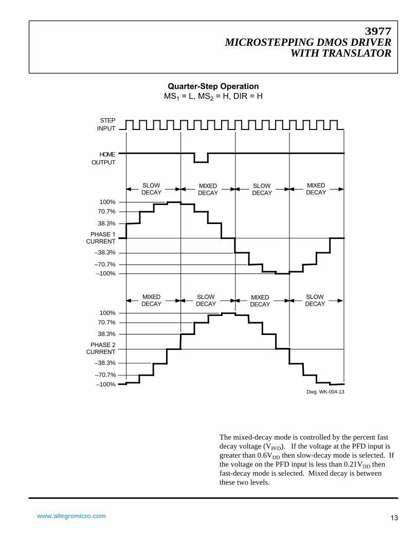
Quarter-Step OperationMS1 = L, MS2 = H, DIR = H
The mixed-decay mode is controlled by the percent fastdecay voltage (VPFD). If the voltage at the PFD input isgreater than 0.6VDD then slow-decay mode is selected. Ifthe voltage on the PFD input is less than 0.21VDD thenfast-decay mode is selected. Mixed decay is betweenthese two levels.
115 Northeast Cutoff, Box 15036Worcester, Massachusetts 01615-0036 (508) 853-5000
3977MICROSTEPPING DMOS DRIVERWITH TRANSLATOR
14
Dwg. WK-004-12
PHASE 2CURRENT
100%
–100%
SLOWDECAY
MIXEDDECAY
SLOWDECAY
MIXEDDECAY
PHASE 1CURRENT
SLOWDECAY
MIXEDDECAY
SLOWDECAY
MIXEDDECAY
STEPINPUT
HOMEOUTPUT
100%
–100%
70.7%
38.3%
–70.7%
–38.3%
70.7%
38.3%
–70.7%
–38.3%
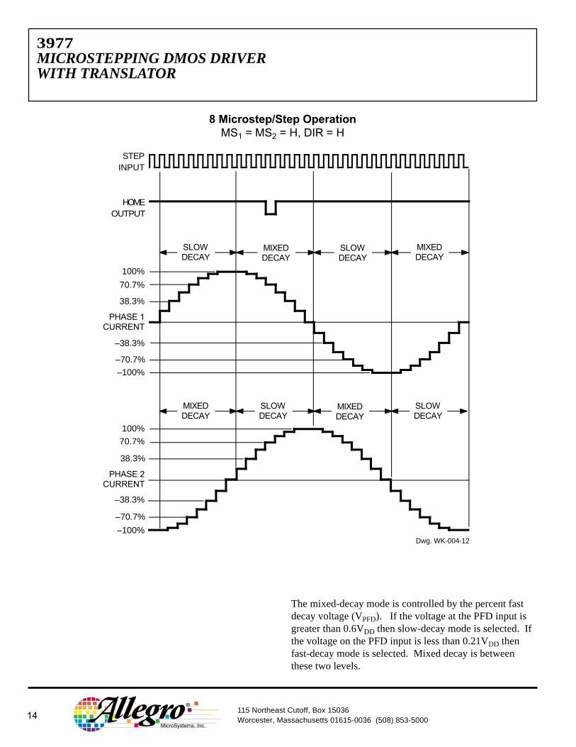
8 Microstep/Step OperationMS1 = MS2 = H, DIR = H
The mixed-decay mode is controlled by the percent fastdecay voltage (VPFD). If the voltage at the PFD input isgreater than 0.6VDD then slow-decay mode is selected. Ifthe voltage on the PFD input is less than 0.21VDD thenfast-decay mode is selected. Mixed decay is betweenthese two levels.
3977MICROSTEPPING DMOS DRIVER
WITH TRANSLATOR
www.allegromicro.com 15
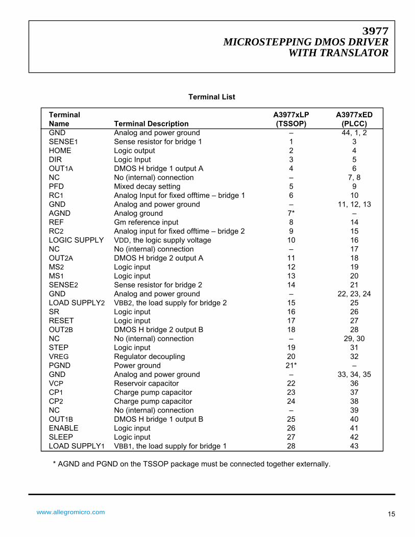
Terminal List
Terminal A3977xLP A3977xEDName Terminal Description (TSSOP) (PLCC)GND Analog and power ground – 44, 1, 2SENSE1 Sense resistor for bridge 1 1 3HOME Logic output 2 4DIR Logic Input 3 5OUT1A DMOS H bridge 1 output A 4 6NC No (internal) connection – 7, 8PFD Mixed decay setting 5 9RC1 Analog Input for fixed offtime – bridge 1 6 10GND Analog and power ground – 11, 12, 13AGND Analog ground 7* –REF Gm reference input 8 14RC2 Analog input for fixed offtime – bridge 2 9 15LOGIC SUPPLY VDD, the logic supply voltage 10 16NC No (internal) connection – 17OUT2A DMOS H bridge 2 output A 11 18MS2 Logic input 12 19MS1 Logic input 13 20SENSE2 Sense resistor for bridge 2 14 21GND Analog and power ground – 22, 23, 24LOAD SUPPLY2 VBB2, the load supply for bridge 2 15 25SR Logic input 16 26RESET Logic input 17 27OUT2B DMOS H bridge 2 output B 18 28NC No (internal) connection – 29, 30STEP Logic input 19 31VREG Regulator decoupling 20 32PGND Power ground 21* –GND Analog and power ground – 33, 34, 35VCP Reservoir capacitor 22 36CP1 Charge pump capacitor 23 37CP2 Charge pump capacitor 24 38NC No (internal) connection – 39OUT1B DMOS H bridge 1 output B 25 40ENABLE Logic input 26 41SLEEP Logic input 27 42LOAD SUPPLY1 VBB1, the load supply for bridge 1 28 43
* AGND and PGND on the TSSOP package must be connected together externally.
115 Northeast Cutoff, Box 15036Worcester, Massachusetts 01615-0036 (508) 853-5000
3977MICROSTEPPING DMOS DRIVERWITH TRANSLATOR
16
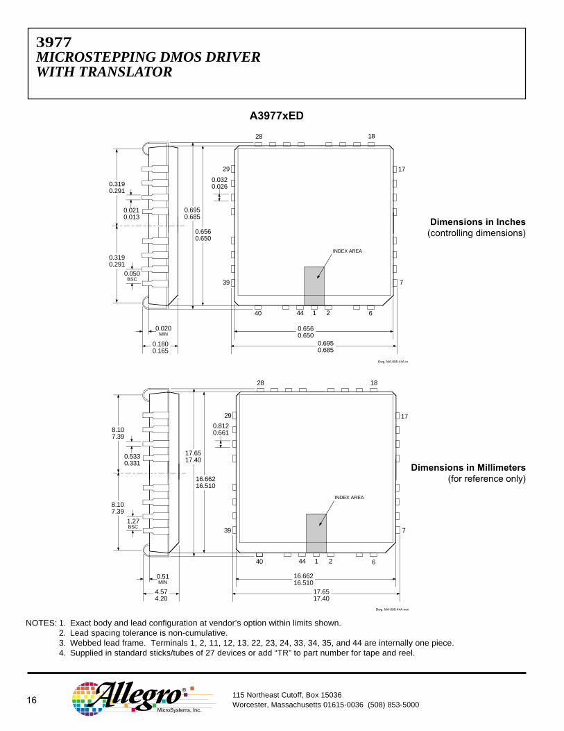
A3977xED
NOTES: 1. Exact body and lead configuration at vendor’s option within limits shown.2. Lead spacing tolerance is non-cumulative.3. Webbed lead frame. Terminals 1, 2, 11, 12, 13, 22, 23, 24, 33, 34, 35, and 44 are internally one piece.4. Supplied in standard sticks/tubes of 27 devices or add “TR” to part number for tape and reel.
1828
Dwg. MA-005-44A in
0.020MIN
0.050BSC
144
0.0210.013
INDEX AREA
2 6
7
1729
39
40
0.6950.685
0.0320.026
0.3190.291
0.3190.291
0.1800.165
0.6950.685
0.6560.650
0.6560.650
Dwg. MA-005-44A mm
17.6517.40
0.51MIN
4.574.20
17.6517.40
16.66216.510
1.27BSC
0.8120.661
144
0.5330.331
INDEX AREA
2
28
29
39
40 6
7
17
18
16.66216.510
8.107.39
8.107.39
Dimensions in Inches(controlling dimensions)
Dimensions in Millimeters(for reference only)
3977MICROSTEPPING DMOS DRIVER
WITH TRANSLATOR
www.allegromicro.com 17
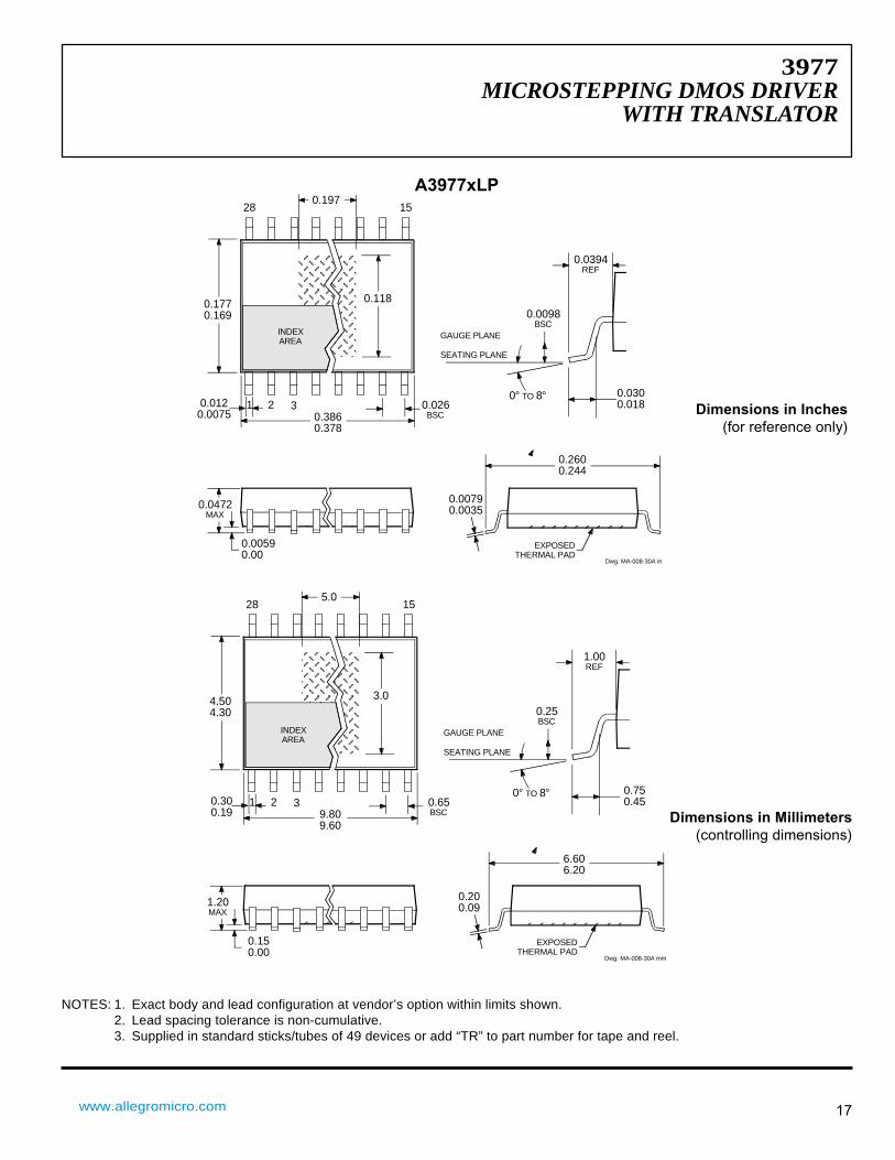
A3977xLP
NOTES: 1. Exact body and lead configuration at vendor’s option within limits shown.2. Lead spacing tolerance is non-cumulative.3. Supplied in standard sticks/tubes of 49 devices or add “TR” to part number for tape and reel.
28 15
1 2 30.3860.378
0.0120.0075
0.0472MAX
0.00590.00
0.026BSC
0.1770.169
0.118
0.197
0.00790.0035
0.0300.018
0° TO 8°
GAUGE PLANE
0.0098BSC
SEATING PLANE
0.0394REF
Dwg. MA-008-30A in
EXPOSEDTHERMAL PAD
INDEXAREA
0.2600.244
28 15
1 2 39.809.60
0.300.19
1.20MAX
0.150.00
Dwg. MA-008-30A mm
0.65BSC
4.504.30
3.0
5.0
0.200.09
6.606.20
0.750.45
0° TO 8°
GAUGE PLANE
0.25BSC
SEATING PLANE
1.00REF
INDEXAREA
EXPOSEDTHERMAL PAD
Dimensions in Inches(for reference only)
Dimensions in Millimeters(controlling dimensions)
115 Northeast Cutoff, Box 15036Worcester, Massachusetts 01615-0036 (508) 853-5000
3977MICROSTEPPING DMOS DRIVERWITH TRANSLATOR
18
The products described here are manufactured under one or moreU.S. patents or U.S. patents pending.
Allegro MicroSystems, Inc. reserves the right to make, from time totime, such departures from the detail specifications as may berequired to permit improvements in the performance, reliability, ormanufacturability of its products. Before placing an order, the user iscautioned to verify that the information being relied upon is current.
Allegro products are not authorized for use as critical componentsin life-support devices or systems without express written approval.
The information included herein is believed to be accurate andreliable. However, Allegro MicroSystems, Inc. assumes no responsi-bility for its use; nor for any infringement of patents or other rights ofthird parties which may result from its use.