Embed Size (px)
Citation preview
1FEATURESDESCRIPTION
APPLICATIONS
0
10
20
30
40
50
60
70
80
90
100
0.01 0.1 1 10
Eff
icie
nc
y -
%
I - Load Current - AL
V = 3.3 VO
V = 12 VI
V = 18 VI
V = 24 VI
V = 28 VI
V = 5 VIPH
VIN
GND
BOOT
VSENSE
COMP
SS
CSS
D1
VIN
VOUT
EN
TPS54331
CI
CBOOT
LO
CO
Ren1
RO2
C1
C2
R3
Ren2
RO1
TPS54331
www.ti.com ...................................................................................................................................................... SLVS839B–JULY 2008–REVISED OCTOBER 2008
3A, 28V INPUT, STEP DOWN SWIFT™ DC/DC CONVERTER WITH ECO-MODE™
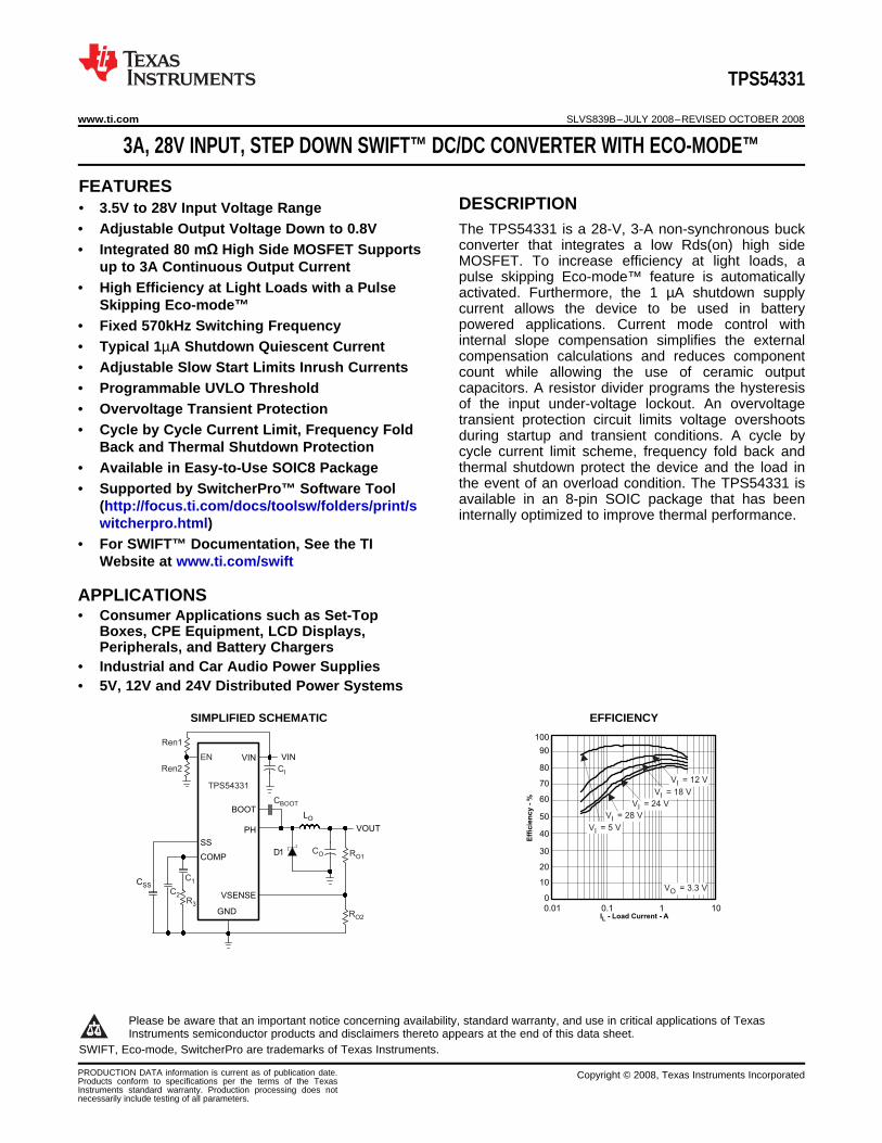
2• 3.5V to 28V Input Voltage Range• Adjustable Output Voltage Down to 0.8V The TPS54331 is a 28-V, 3-A non-synchronous buck
converter that integrates a low Rds(on) high side• Integrated 80 mΩ High Side MOSFET SupportsMOSFET. To increase efficiency at light loads, aup to 3A Continuous Output Currentpulse skipping Eco-mode™ feature is automatically
• High Efficiency at Light Loads with a Pulse activated. Furthermore, the 1 µA shutdown supplySkipping Eco-mode™ current allows the device to be used in battery
powered applications. Current mode control with• Fixed 570kHz Switching Frequencyinternal slope compensation simplifies the external• Typical 1µA Shutdown Quiescent Current compensation calculations and reduces component
• Adjustable Slow Start Limits Inrush Currents count while allowing the use of ceramic outputcapacitors. A resistor divider programs the hysteresis• Programmable UVLO Thresholdof the input under-voltage lockout. An overvoltage• Overvoltage Transient Protectiontransient protection circuit limits voltage overshoots
• Cycle by Cycle Current Limit, Frequency Fold during startup and transient conditions. A cycle byBack and Thermal Shutdown Protection cycle current limit scheme, frequency fold back and
thermal shutdown protect the device and the load in• Available in Easy-to-Use SOIC8 Packagethe event of an overload condition. The TPS54331 is• Supported by SwitcherPro™ Software Toolavailable in an 8-pin SOIC package that has been(http://focus.ti.com/docs/toolsw/folders/print/s internally optimized to improve thermal performance.witcherpro.html)
• For SWIFT™ Documentation, See the TIWebsite at www.ti.com/swift
• Consumer Applications such as Set-TopBoxes, CPE Equipment, LCD Displays,Peripherals, and Battery Chargers
• Industrial and Car Audio Power Supplies• 5V, 12V and 24V Distributed Power Systems
SIMPLIFIED SCHEMATIC EFFICIENCY
1
Please be aware that an important notice concerning availability, standard warranty, and use in critical applications of TexasInstruments semiconductor products and disclaimers thereto appears at the end of this data sheet.
2SWIFT, Eco-mode, SwitcherPro are trademarks of Texas Instruments.
PRODUCTION DATA information is current as of publication date. Copyright © 2008, Texas Instruments IncorporatedProducts conform to specifications per the terms of the TexasInstruments standard warranty. Production processing does notnecessarily include testing of all parameters.
ABSOLUTE MAXIMUM RATINGS (1)
PACKAGE DISSIPATION RATINGS (1) (2) (3)
TPS54331
SLVS839B–JULY 2008–REVISED OCTOBER 2008 ...................................................................................................................................................... www.ti.com
These devices have limited built-in ESD protection. The leads should be shorted together or the device placed in conductive foamduring storage or handling to prevent electrostatic damage to the MOS gates.
ORDERING INFORMATION (1)
TJ PACKAGE SWITCHING FREQUENCY PART NUMBER (2)
–40°C to 150°C 8 pin SOIC 570 kHz TPS54331D
(1) For the most current package and ordering information, see the Package Option Addendum at the end of this document, or see the TIweb site at www.ti.com.
(2) The D package is also available taped and reeled. Add an R suffix to the device type (i.e., TPS54331DR). See applications section ofdata sheet for layout information.
over operating free-air temperature range (unless otherwise noted)
VALUE UNITVIN –0.3 to 30EN –0.3 to 5BOOT 38
Input Voltage VVSENSE –0.3 to 3COMP –0.3 to 3SS –0.3 to 3BOOT-PH 8
Output Voltage PH –0.6 to 30 VPH (10 ns transient from ground to negative peak) –5EN 100 µABOOT 100 mA
Source CurrentVSENSE 10 µAPH 9 AVIN 9 A
Sink Current COMP 100µA
SS 200Electrostatic Discharge (HBM) 2 kVElectrostatic Discharge (CDM) 500 VOperating Junction Temperature –40 to 150 °CStorage Temperature –65 to 150 °C
(1) Stresses beyond those listed under absolute maximum ratings may cause permanent damage to the device. These are stress ratingsonly, and functional operation of the device at these or any other conditions beyond those indicated under recommended operatingconditions is not implied. Exposure to absolute-maximum-rated conditions for extended periods may affect device reliability.
PACKAGE THERMAL IMPEDANCE JUNCTION TO PSEUDO THERMAL IMPEDANCE JUNCTION TOAMBIENT TOP
SOIC8 100 °C/W 5 °C/W
(1) Maximum power dissipation may be limited by overcurrent protection(2) Power rating at a specific ambient temperature TA should be determined with a junction temperature of 150°C. This is the point where
distortion starts to substantially increase. Thermal management of the PCB should strive to keep the junction temperature at or below150°C for best performance and long-term reliability. See power dissipation estimate in application section of this data sheet for moreinformation.
(3) Test board conditions:a. 2 inches x 1.5 inches, 2 layers, thickness: 0.062 inchb. 2-ounce copper traces located on the top and bottom of the PCBc. 6 thermal vias located under the device package
2 Submit Documentation Feedback Copyright © 2008, Texas Instruments Incorporated
Product Folder Link(s): TPS54331
RECOMMENDED OPERATING CONDITIONS
ELECTRICAL CHARACTERISTICS
TPS54331
www.ti.com ...................................................................................................................................................... SLVS839B–JULY 2008–REVISED OCTOBER 2008
over operating free-air temperature range (unless otherwise noted)
MIN TYP MAX UNITOperating Input Voltage on (VIN pin) 3.5 28 VOperating junction temperature, TJ –40 150 °C
TJ = –40°C to 150°C, VIN = 3.5V to 28V (unless otherwise noted)
DESCRIPTION TEST CONDITIONS MIN TYP MAX UNITSUPPLY VOLTAGE (VIN PIN)Internal undervoltage lockout threshold Rising and Falling 3.5 VShutdown supply current EN = 0V, VIN = 12V, –40°C to 85°C 1 4 µAOperating – non switching supply current VSENSE = 0.85 V 110 190 µAENABLE AND UVLO (EN PIN)Enable threshold Rising and Falling 1.25 1.35 VInput current Enable threshold – 50 mV -1 µAInput current Enable threshold + 50 mV -4 µAVOLTAGE REFERENCEVoltage reference 0.772 0.8 0.828 VHIGH-SIDE MOSFETOn resistance BOOT-PH = 3 V, VIN = 3.5 V 115 200 mΩ
BOOT-PH = 6 V, VIN = 12 V 80 150ERROR AMPLIFIERError amplifier transconductance (gm) –2 µA < ICOMP < 2 µA, V(COMP) = 1 V 92 µmhosError amplifier DC gain (1) VSENSE = 0.8 V 800 V/VError amplifier unity gain bandwidth (1) 5 pF capacitance from COMP to GND pins 2.7 MHzError amplifier source/sink current V(COMP) = 1.0 V, 100 mV overdrive ±7 µASwitch current to COMP transconductance VIN = 12 V 12 A/VSWITCHING FREQUENCYTPS54331 Switching Frequency VIN = 12V, 25°C 456 570 684 kHzMinimum controllable on time VIN = 12V, 25°C 105 130 nsMaximum controllable duty ratio (1) BOOT-PH = 6 V 90 93 %PULSE SKIPPING ECO-MODE™Pulse skipping Eco-mode™ switch current threshold 160 mACURRENT LIMITCurrent limit threshold VIN = 12 V 3.5 5.8 ATHERMAL SHUTDOWNThermal Shutdown 165 °CSLOW START (SS PIN)Charge current V(SS) = 0.4 V 2 µASS to VSENSE matching V(SS) = 0.4 V 10 mV
(1) Specified by design
Copyright © 2008, Texas Instruments Incorporated Submit Documentation Feedback 3
Product Folder Link(s): TPS54331
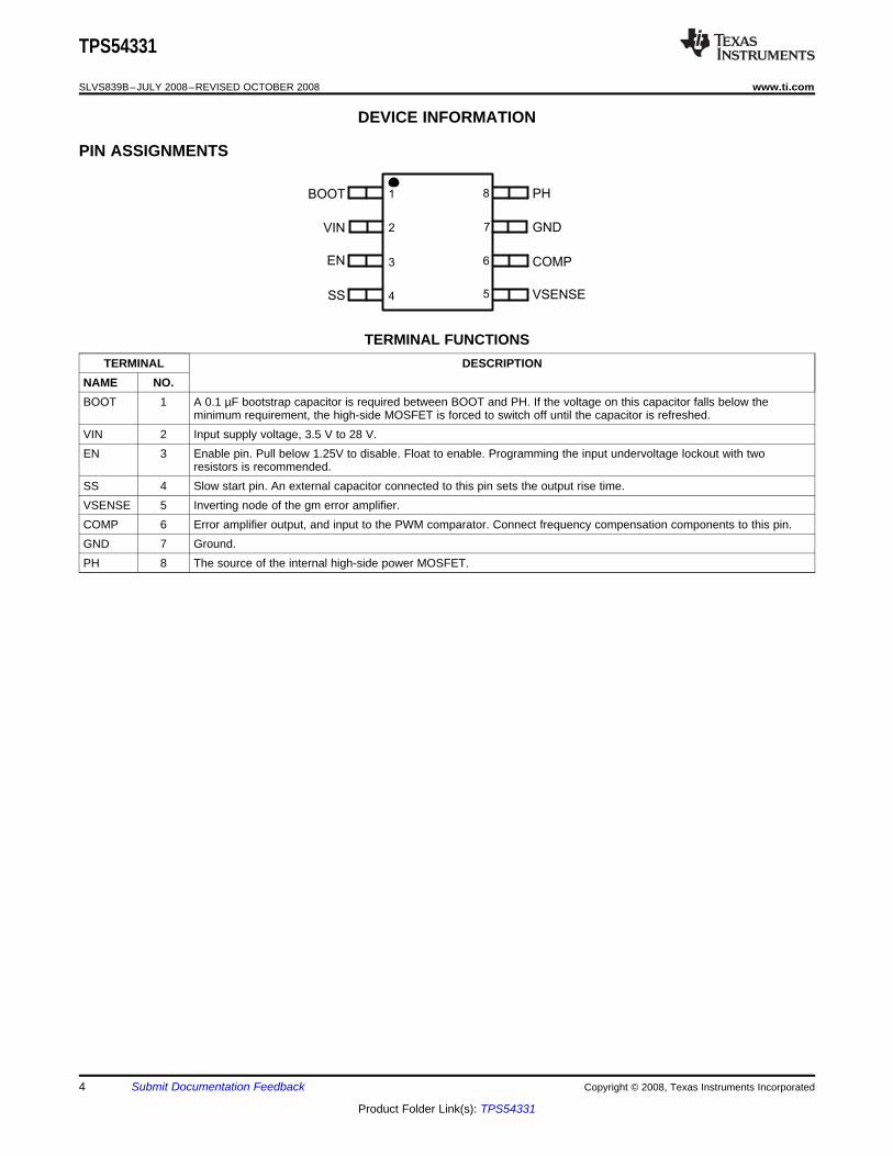
DEVICE INFORMATION
PIN ASSIGNMENTS
1
2
3
4 5
6
7
8BOOT
VIN
EN
SS
PH
GND
COMP
VSENSE
TPS54331
SLVS839B–JULY 2008–REVISED OCTOBER 2008 ...................................................................................................................................................... www.ti.com
TERMINAL FUNCTIONSTERMINAL DESCRIPTION
NAME NO.BOOT 1 A 0.1 µF bootstrap capacitor is required between BOOT and PH. If the voltage on this capacitor falls below the
minimum requirement, the high-side MOSFET is forced to switch off until the capacitor is refreshed.VIN 2 Input supply voltage, 3.5 V to 28 V.EN 3 Enable pin. Pull below 1.25V to disable. Float to enable. Programming the input undervoltage lockout with two
resistors is recommended.SS 4 Slow start pin. An external capacitor connected to this pin sets the output rise time.VSENSE 5 Inverting node of the gm error amplifier.COMP 6 Error amplifier output, and input to the PWM comparator. Connect frequency compensation components to this pin.GND 7 Ground.PH 8 The source of the internal high-side power MOSFET.
4 Submit Documentation Feedback Copyright © 2008, Texas Instruments Incorporated
Product Folder Link(s): TPS54331
ErrorAmplifier
R Q
S
BootCharge
BootUVLO
CurrentSense
OscillatorFrequency
Shift
GateDriveLogic
SlopeCompensation
PWMLatch
PWMComparator
ECO-MODEMinimum Clamp
™
MaximumClamp
VoltageReference
DischargeLogic
VSENSE
COMP
PH
BOOT
VIN
GND
ThermalShutdown
EN
EnableComparator
ShutdownLogic
Shutdown
EnableThreshold
S
1.25 V
0.8 V
80 mW
165C
2.1V
12 A/V
SS
Shutdown
VSENSE
1 Am 3 Am
gm = 92 A/VDC gain = 800 V/V
BW = 2.7 MHz
m
2 kW
2 Am
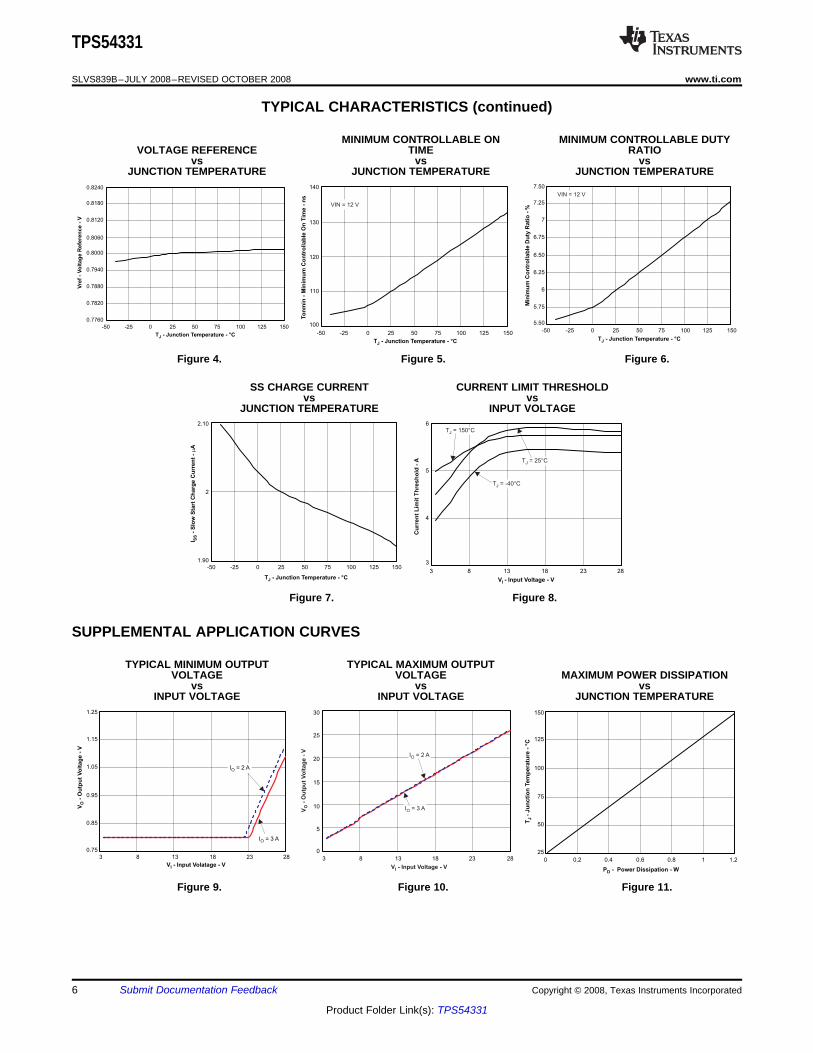
TYPICAL CHARACTERISTICS
CHARACTERIZATION CURVES
60
65
70
75
80
85
90
95
100
105
110
-50 -25 0 25 50 75 100 125 150
T - Junction Temperature - °CJ
Rd
so
n -
On
Resis
tan
ce -
mW
VIN = 12 V
0
1
2
3
4
3 8 13 18 23 28
V - Input Voltage - VI
Isd
- S
hu
tdo
wn
Cu
rren
t -
Am
EN = 0 V
T = 150°CJ
T = 25°CJ
T = -40°CJ
550
555
560
565
570
575
580
585
590
-50 -25 0 25 50 75 100 125 150
fsw
- O
scilla
tor
Fre
qu
en
cy -
kH
z
T - Junction Temperature - °CJ
VIN = 12 V
TPS54331
www.ti.com ...................................................................................................................................................... SLVS839B–JULY 2008–REVISED OCTOBER 2008
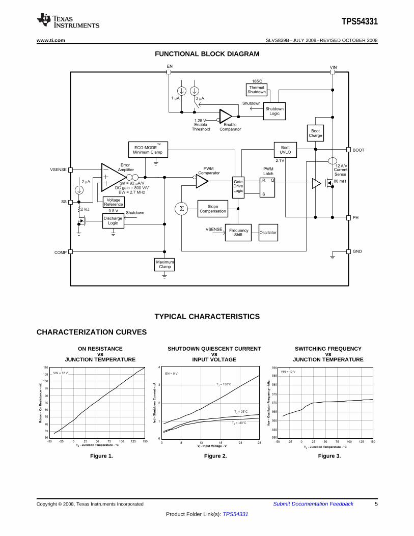
FUNCTIONAL BLOCK DIAGRAM
ON RESISTANCE SHUTDOWN QUIESCENT CURRENT SWITCHING FREQUENCYvs vs vs
JUNCTION TEMPERATURE INPUT VOLTAGE JUNCTION TEMPERATURE
Figure 1. Figure 2. Figure 3.
Copyright © 2008, Texas Instruments Incorporated Submit Documentation Feedback 5
Product Folder Link(s): TPS54331
0.7760
0.7820
0.7880
0.7940
0.8000
0.8060
0.8120
0.8180
0.8240
-50 -25 0 25 50 75 100 125 150
Vre
f -
Vo
lta
ge
Re
fere
nc
e -
V
T - Junction Temperature - °CJ
5.50
5.75
6
6.25
6.50
6.75
7
7.25
7.50
-50 -25 0 25 50 75 100 125 150
Min
imu
m C
on
tro
llab
le D
uty
Rati
o -
%
T - Junction Temperature - °CJ
VIN = 12 V
100
110
120
130
140
-50 -25 0 25 50 75 100 125 150
To
nm
in -
Min
imu
m C
on
tro
llab
le O
n T
ime -
ns
T - Junction Temperature - °CJ
VIN = 12 V
1.90
2
2.10
-50 -25 0 25 50 75 100 125 150
I-
Slo
w S
tart
Ch
arg
e C
urr
en
t -
AS
Sm
T - Junction Temperature - °CJ
3
4
5
6
3 8 13 18 23 28
V - Input Voltage - VI
Cu
rre
nt
Lim
it T
hre
sh
old
-A
T = 150°CJ
T = 25°CJ
T = -40°CJ
SUPPLEMENTAL APPLICATION CURVES
3 8 13 18 23 28
V-
Ou
tpu
t V
olt
ag
e -
VO
V - Input Volatage - VI
0.75
0.85
0.95
1.05
1.15
1.25
I = 2 AO
I = 3 AO
3 8 13 18 23 28
0
5
10
15
20
25
30
V-
Ou
tpu
t V
olt
ag
e -
VO
V - Input Voltage - VI
I = 2 AO
I = 3 AO
25
50
75
100
125
150
0 0.2 0.4 0.6 0.8 1 1.2
P - Power Dissipation - WD
T-
Ju
ncti
on
Tem
pera
ture
- °
CJ
TPS54331
SLVS839B–JULY 2008–REVISED OCTOBER 2008 ...................................................................................................................................................... www.ti.com
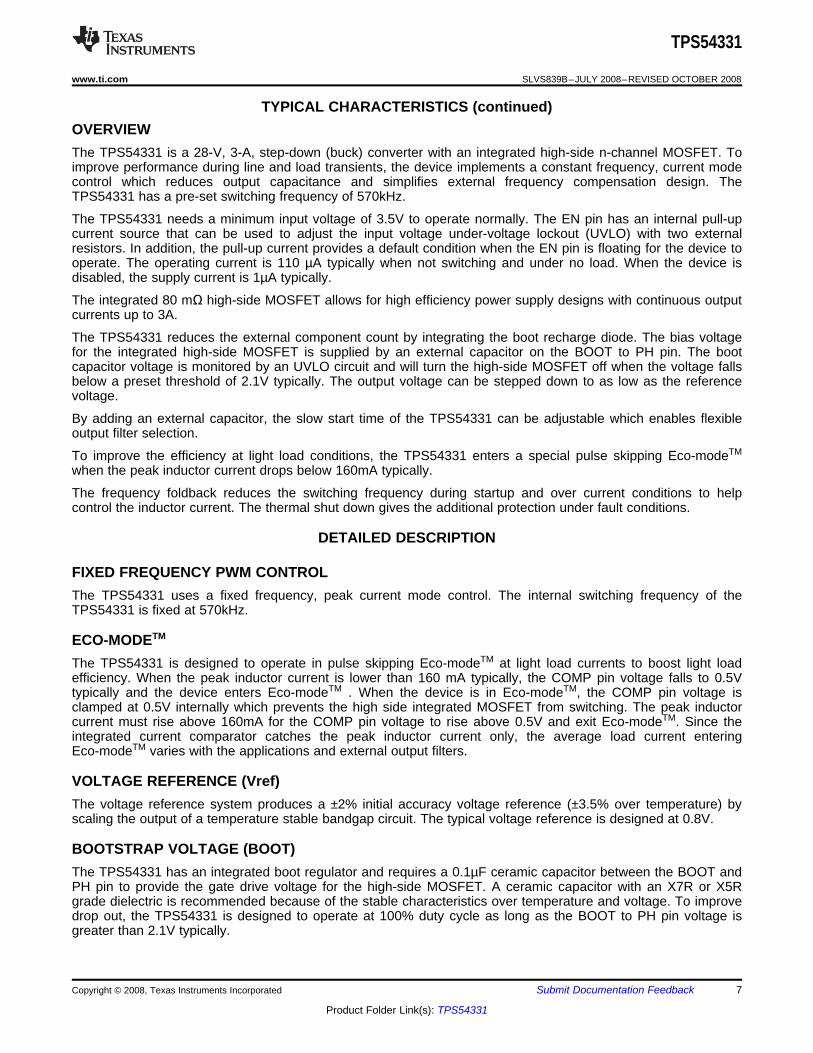
TYPICAL CHARACTERISTICS (continued)
MINIMUM CONTROLLABLE ON MINIMUM CONTROLLABLE DUTYVOLTAGE REFERENCE TIME RATIO
vs vs vsJUNCTION TEMPERATURE JUNCTION TEMPERATURE JUNCTION TEMPERATURE
Figure 4. Figure 5. Figure 6.
SS CHARGE CURRENT CURRENT LIMIT THRESHOLDvs vs
JUNCTION TEMPERATURE INPUT VOLTAGE
Figure 7. Figure 8.
TYPICAL MINIMUM OUTPUT TYPICAL MAXIMUM OUTPUTVOLTAGE VOLTAGE MAXIMUM POWER DISSIPATION
vs vs vsINPUT VOLTAGE INPUT VOLTAGE JUNCTION TEMPERATURE
Figure 9. Figure 10. Figure 11.
6 Submit Documentation Feedback Copyright © 2008, Texas Instruments Incorporated
Product Folder Link(s): TPS54331
OVERVIEW
DETAILED DESCRIPTION
FIXED FREQUENCY PWM CONTROL
ECO-MODETM
VOLTAGE REFERENCE (Vref)
BOOTSTRAP VOLTAGE (BOOT)
TPS54331
www.ti.com ...................................................................................................................................................... SLVS839B–JULY 2008–REVISED OCTOBER 2008
TYPICAL CHARACTERISTICS (continued)
The TPS54331 is a 28-V, 3-A, step-down (buck) converter with an integrated high-side n-channel MOSFET. Toimprove performance during line and load transients, the device implements a constant frequency, current modecontrol which reduces output capacitance and simplifies external frequency compensation design. TheTPS54331 has a pre-set switching frequency of 570kHz.
The TPS54331 needs a minimum input voltage of 3.5V to operate normally. The EN pin has an internal pull-upcurrent source that can be used to adjust the input voltage under-voltage lockout (UVLO) with two externalresistors. In addition, the pull-up current provides a default condition when the EN pin is floating for the device tooperate. The operating current is 110 µA typically when not switching and under no load. When the device isdisabled, the supply current is 1µA typically.
The integrated 80 mΩ high-side MOSFET allows for high efficiency power supply designs with continuous outputcurrents up to 3A.
The TPS54331 reduces the external component count by integrating the boot recharge diode. The bias voltagefor the integrated high-side MOSFET is supplied by an external capacitor on the BOOT to PH pin. The bootcapacitor voltage is monitored by an UVLO circuit and will turn the high-side MOSFET off when the voltage fallsbelow a preset threshold of 2.1V typically. The output voltage can be stepped down to as low as the referencevoltage.
By adding an external capacitor, the slow start time of the TPS54331 can be adjustable which enables flexibleoutput filter selection.
To improve the efficiency at light load conditions, the TPS54331 enters a special pulse skipping Eco-modeTM
when the peak inductor current drops below 160mA typically.
The frequency foldback reduces the switching frequency during startup and over current conditions to helpcontrol the inductor current. The thermal shut down gives the additional protection under fault conditions.
The TPS54331 uses a fixed frequency, peak current mode control. The internal switching frequency of theTPS54331 is fixed at 570kHz.
The TPS54331 is designed to operate in pulse skipping Eco-modeTM at light load currents to boost light loadefficiency. When the peak inductor current is lower than 160 mA typically, the COMP pin voltage falls to 0.5Vtypically and the device enters Eco-modeTM . When the device is in Eco-modeTM, the COMP pin voltage isclamped at 0.5V internally which prevents the high side integrated MOSFET from switching. The peak inductorcurrent must rise above 160mA for the COMP pin voltage to rise above 0.5V and exit Eco-modeTM. Since theintegrated current comparator catches the peak inductor current only, the average load current enteringEco-modeTM varies with the applications and external output filters.
The voltage reference system produces a ±2% initial accuracy voltage reference (±3.5% over temperature) byscaling the output of a temperature stable bandgap circuit. The typical voltage reference is designed at 0.8V.
The TPS54331 has an integrated boot regulator and requires a 0.1µF ceramic capacitor between the BOOT andPH pin to provide the gate drive voltage for the high-side MOSFET. A ceramic capacitor with an X7R or X5Rgrade dielectric is recommended because of the stable characteristics over temperature and voltage. To improvedrop out, the TPS54331 is designed to operate at 100% duty cycle as long as the BOOT to PH pin voltage isgreater than 2.1V typically.
Copyright © 2008, Texas Instruments Incorporated Submit Documentation Feedback 7
Product Folder Link(s): TPS54331
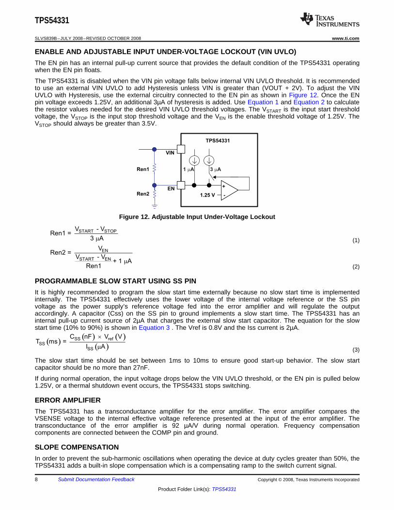
ENABLE AND ADJUSTABLE INPUT UNDER-VOLTAGE LOCKOUT (VIN UVLO)
EN
1.25 V
VIN
+
-
Ren1
Ren2
TPS54331
1 Am 3 Am
START STOPV - VRen1 =
3 Am (1)
EN
START EN
VRen2 =
V - V+ 1 A
Ren1m
(2)
PROGRAMMABLE SLOW START USING SS PIN
( )( ) ( )
( )SS ref
SS
SS
C nF V VT ms =
I A
´
m (3)
ERROR AMPLIFIER
SLOPE COMPENSATION
TPS54331
SLVS839B–JULY 2008–REVISED OCTOBER 2008 ...................................................................................................................................................... www.ti.com
The EN pin has an internal pull-up current source that provides the default condition of the TPS54331 operatingwhen the EN pin floats.
The TPS54331 is disabled when the VIN pin voltage falls below internal VIN UVLO threshold. It is recommendedto use an external VIN UVLO to add Hysteresis unless VIN is greater than (VOUT + 2V). To adjust the VINUVLO with Hysteresis, use the external circuitry connected to the EN pin as shown in Figure 12. Once the ENpin voltage exceeds 1.25V, an additional 3µA of hysteresis is added. Use Equation 1 and Equation 2 to calculatethe resistor values needed for the desired VIN UVLO threshold voltages. The VSTART is the input start thresholdvoltage, the VSTOP is the input stop threshold voltage and the VEN is the enable threshold voltage of 1.25V. TheVSTOP should always be greater than 3.5V.
Figure 12. Adjustable Input Under-Voltage Lockout
It is highly recommended to program the slow start time externally because no slow start time is implementedinternally. The TPS54331 effectively uses the lower voltage of the internal voltage reference or the SS pinvoltage as the power supply’s reference voltage fed into the error amplifier and will regulate the outputaccordingly. A capacitor (Css) on the SS pin to ground implements a slow start time. The TPS54331 has aninternal pull-up current source of 2µA that charges the external slow start capacitor. The equation for the slowstart time (10% to 90%) is shown in Equation 3 . The Vref is 0.8V and the Iss current is 2µA.
The slow start time should be set between 1ms to 10ms to ensure good start-up behavior. The slow startcapacitor should be no more than 27nF.
If during normal operation, the input voltage drops below the VIN UVLO threshold, or the EN pin is pulled below1.25V, or a thermal shutdown event occurs, the TPS54331 stops switching.
The TPS54331 has a transconductance amplifier for the error amplifier. The error amplifier compares theVSENSE voltage to the internal effective voltage reference presented at the input of the error amplifier. Thetransconductance of the error amplifier is 92 µA/V during normal operation. Frequency compensationcomponents are connected between the COMP pin and ground.
In order to prevent the sub-harmonic oscillations when operating the device at duty cycles greater than 50%, theTPS54331 adds a built-in slope compensation which is a compensating ramp to the switch current signal.
8 Submit Documentation Feedback Copyright © 2008, Texas Instruments Incorporated
Product Folder Link(s): TPS54331
CURRENT MODE COMPENSATION DESIGN
OVERCURRENT PROTECTION AND FREQUENCY SHIFT
OVERVOLTAGE TRANSIENT PROTECTION
THERMAL SHUTDOWN
TPS54331
www.ti.com ...................................................................................................................................................... SLVS839B–JULY 2008–REVISED OCTOBER 2008
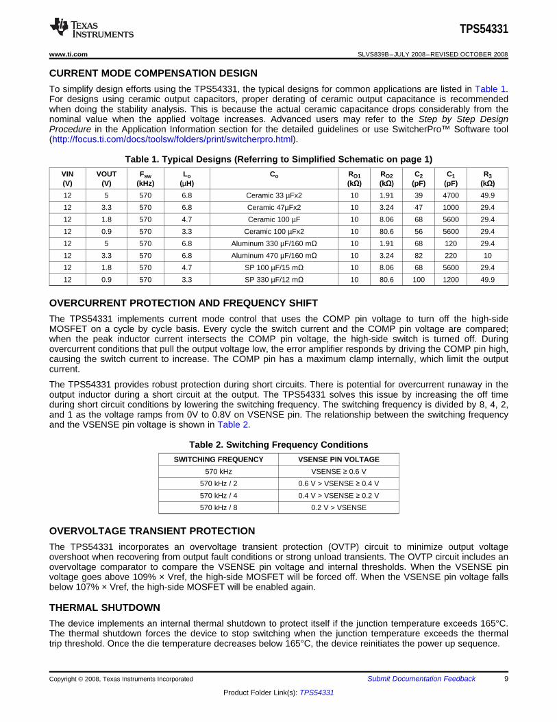
To simplify design efforts using the TPS54331, the typical designs for common applications are listed in Table 1.For designs using ceramic output capacitors, proper derating of ceramic output capacitance is recommendedwhen doing the stability analysis. This is because the actual ceramic capacitance drops considerably from thenominal value when the applied voltage increases. Advanced users may refer to the Step by Step DesignProcedure in the Application Information section for the detailed guidelines or use SwitcherPro™ Software tool(http://focus.ti.com/docs/toolsw/folders/print/switcherpro.html).
Table 1. Typical Designs (Referring to Simplified Schematic on page 1)VIN VOUT Fsw Lo Co RO1 RO2 C2 C1 R3(V) (V) (kHz) (µH) (kΩ) (kΩ) (pF) (pF) (kΩ)12 5 570 6.8 Ceramic 33 µFx2 10 1.91 39 4700 49.912 3.3 570 6.8 Ceramic 47µFx2 10 3.24 47 1000 29.412 1.8 570 4.7 Ceramic 100 µF 10 8.06 68 5600 29.412 0.9 570 3.3 Ceramic 100 µFx2 10 80.6 56 5600 29.412 5 570 6.8 Aluminum 330 µF/160 mΩ 10 1.91 68 120 29.412 3.3 570 6.8 Aluminum 470 µF/160 mΩ 10 3.24 82 220 1012 1.8 570 4.7 SP 100 µF/15 mΩ 10 8.06 68 5600 29.412 0.9 570 3.3 SP 330 µF/12 mΩ 10 80.6 100 1200 49.9
The TPS54331 implements current mode control that uses the COMP pin voltage to turn off the high-sideMOSFET on a cycle by cycle basis. Every cycle the switch current and the COMP pin voltage are compared;when the peak inductor current intersects the COMP pin voltage, the high-side switch is turned off. Duringovercurrent conditions that pull the output voltage low, the error amplifier responds by driving the COMP pin high,causing the switch current to increase. The COMP pin has a maximum clamp internally, which limit the outputcurrent.
The TPS54331 provides robust protection during short circuits. There is potential for overcurrent runaway in theoutput inductor during a short circuit at the output. The TPS54331 solves this issue by increasing the off timeduring short circuit conditions by lowering the switching frequency. The switching frequency is divided by 8, 4, 2,and 1 as the voltage ramps from 0V to 0.8V on VSENSE pin. The relationship between the switching frequencyand the VSENSE pin voltage is shown in Table 2.
Table 2. Switching Frequency ConditionsSWITCHING FREQUENCY VSENSE PIN VOLTAGE
570 kHz VSENSE ≥ 0.6 V570 kHz / 2 0.6 V > VSENSE ≥ 0.4 V570 kHz / 4 0.4 V > VSENSE ≥ 0.2 V570 kHz / 8 0.2 V > VSENSE
The TPS54331 incorporates an overvoltage transient protection (OVTP) circuit to minimize output voltageovershoot when recovering from output fault conditions or strong unload transients. The OVTP circuit includes anovervoltage comparator to compare the VSENSE pin voltage and internal thresholds. When the VSENSE pinvoltage goes above 109% × Vref, the high-side MOSFET will be forced off. When the VSENSE pin voltage fallsbelow 107% × Vref, the high-side MOSFET will be enabled again.
The device implements an internal thermal shutdown to protect itself if the junction temperature exceeds 165°C.The thermal shutdown forces the device to stop switching when the junction temperature exceeds the thermaltrip threshold. Once the die temperature decreases below 165°C, the device reinitiates the power up sequence.
Copyright © 2008, Texas Instruments Incorporated Submit Documentation Feedback 9
Product Folder Link(s): TPS54331
APPLICATION INFORMATION
0.01 µF
4.7µF 4.7µF
Vin 7 V 28 V–
0.01 μF
0.1 μF
332 kΩ
68.1 kΩ
47 pF
0Ω47 µF
Vout 3.3 V
Iout Max 3 A6.8 µH
10.2 kΩ
3.24 kΩ29.4 kΩ
1000 pF
47 µF
STEP BY STEP DESIGN PROCEDURE
SWITCHING FREQUENCY
TPS54331
SLVS839B–JULY 2008–REVISED OCTOBER 2008 ...................................................................................................................................................... www.ti.com
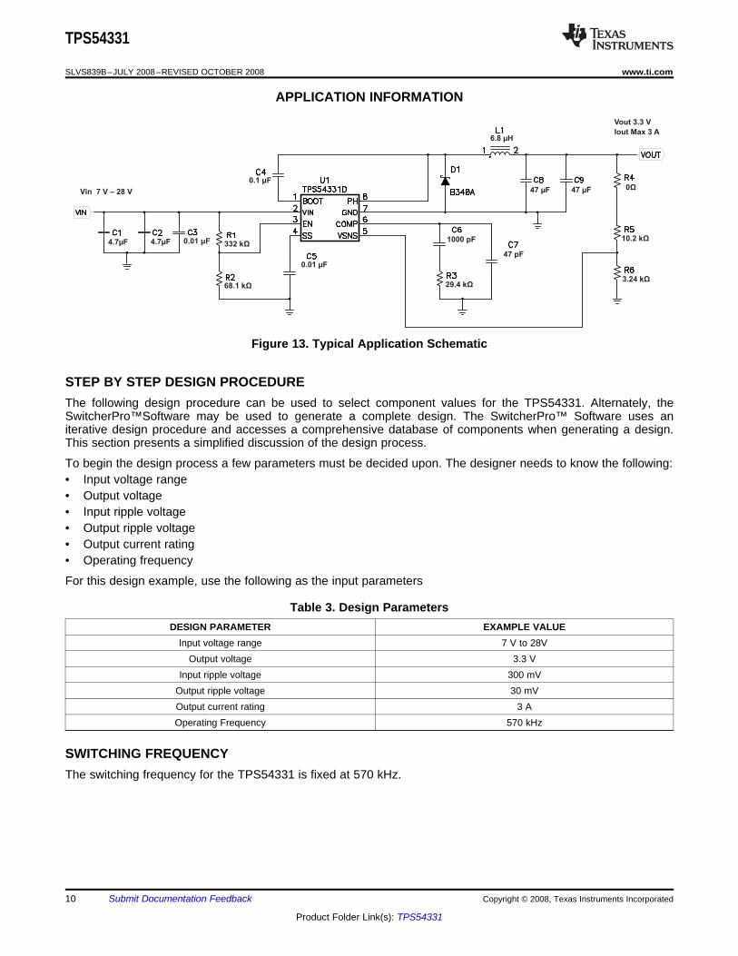
Figure 13. Typical Application Schematic
The following design procedure can be used to select component values for the TPS54331. Alternately, theSwitcherPro™Software may be used to generate a complete design. The SwitcherPro™ Software uses aniterative design procedure and accesses a comprehensive database of components when generating a design.This section presents a simplified discussion of the design process.
To begin the design process a few parameters must be decided upon. The designer needs to know the following:• Input voltage range• Output voltage• Input ripple voltage• Output ripple voltage• Output current rating• Operating frequency
For this design example, use the following as the input parameters
Table 3. Design ParametersDESIGN PARAMETER EXAMPLE VALUE
Input voltage range 7 V to 28VOutput voltage 3.3 V
Input ripple voltage 300 mVOutput ripple voltage 30 mVOutput current rating 3 AOperating Frequency 570 kHz
The switching frequency for the TPS54331 is fixed at 570 kHz.
10 Submit Documentation Feedback Copyright © 2008, Texas Instruments Incorporated
Product Folder Link(s): TPS54331
OUTPUT VOLTAGE SET POINT
REF
OUT REF
R5 VR6 =
V V
´
- (4)
OUT REF
R5V = V +1
R6
é ù´ ê ú
ë û (5)
INPUT CAPACITORS
( )OUT(MAX)IN OUT(MAX) MAX
BULK SW
I 0.25V = + I ESR
C f
´D ´
´ (6)
2
OUT(MAX)CIN
II =
(7)
OUTPUT FILTER COMPONENTS
Inductor Selection
TPS54331
www.ti.com ...................................................................................................................................................... SLVS839B–JULY 2008–REVISED OCTOBER 2008
The output voltage of the TPS54331 is externally adjustable using a resistor divider network. In the applicationcircuit of Figure 13, this divider network is comprised of R5 and R6. The relationship of the output voltage to theresistor divider is given by Equation 4 and Equation 5:
Choose R5 to be approximately 10.0 kΩ. Slightly increasing or decreasing R5 can result in closer output voltagematching when using standard value resistors. In this design, R4 = 10.2 kΩ and R = 3.24 kΩ, resulting in a 3.31V output voltage. The zero ohm resistor R4 is provided as a convenient place to break the control loop forstability testing.
The TPS54331 requires an input decoupling capacitor and depending on the application, a bulk input capacitor.The typical recommended value for the decoupling capacitor is 10 µF. A high-quality ceramic type X5R or X7R isrecommended. The voltage rating should be greater than the maximum input voltage. A smaller value may beused as long as all other requirements are met; however 10 µF has been shown to work well in a wide variety ofcircuits. Additionally, some bulk capacitance may be needed, especially if the TPS54331 circuit is not locatedwithin about 2 inches from the input voltage source. The value for this capacitor is not critical but should be ratedto handle the maximum input voltage including ripple voltage, and should filter the output so that input ripplevoltage is acceptable. For this design two 4.7 µF capacitors are used for the input decoupling capacitor. They areX7R dielectric rated for 50 V. The equivalent series resistance (ESR) is approximately 2mΩ, and the currentrating is 3 A. Additionally, a small 0.01 µF capacitor is included for high frequency filtering.
This input ripple voltage can be approximated by Equation 6
Where IOUT(MAX) is the maximum load current, fSW is the switching frequency, CBULK is the bulk capacitor valueand ESRMAX is the maximum series resistance of the bulk capacitor.
The maximum RMS ripple current also needs to be checked. For worst case conditions, this can beapproximated by Equation 7
In this case, the input ripple voltage would be 143 mV and the RMS ripple current would be 1.5 A. It is alsoimportant to note that the actual input voltage ripple will be greatly affected by parasitics associated with thelayout and the output impedance of the voltage source. The actual input voltage ripple for this circuit is shown inDesign Parameters and is larger than the calculated value. This measured value is still below the specified inputlimit of 300 mV. The maximum voltage across the input capacitors would be VIN max plus ΔVIN/2. The chosenbulk and bypass capacitors are each rated for 50 V and the ripple current capacity is greater than 3 A, bothproviding ample margin. It is very important that the maximum ratings for voltage and current are not exceededunder any circumstance.
Two components need to be selected for the output filter, L1 and C2. Since the TPS54331 is an externallycompensated device, a wide range of filter component types and values can be supported.
To calculate the minimum value of the output inductor, use Equation 8
Copyright © 2008, Texas Instruments Incorporated Submit Documentation Feedback 11
Product Folder Link(s): TPS54331
( )OUT(MAX) IN(MAX) OUT
MININ(MAX) IND OUT SW
V V VL =
V K I F
´ -
´ ´ ´ (8)
( )2
OUT IN(MAX) OUT2L(RMS) OUT(MAX)
IN(MAX) OUT SW
V V V1I = I +
12 V L F 0.8
æ ö´ -ç ÷´ç ÷´ ´ ´è ø (9)
( )OUT IN(MAX) OUT
L(PK) OUT(MAX)IN(MAX) OUT SW
V V VI = I +
1.6 V L F
´ -
´ ´ ´(10)
Capacitor Selection
)2/(1 max_min_ COOOFRC ´´´= p
(11)
úû
ùêë
é+
´´
-=
ESR
OSW
LPPOPPR
CF
DIV
4
)5.0(
(12)
TPS54331
SLVS839B–JULY 2008–REVISED OCTOBER 2008 ...................................................................................................................................................... www.ti.com
KIND is a coefficient that represents the amount of inductor ripple current relative to the maximum output current.In general, this value is at the discretion of the designer; however, the following guidelines may be used. Fordesigns using low ESR output capacitors such as ceramics, a value as high as KIND = 0.3 may be used. Whenusing higher ESR output capacitors, KIND = 0.2 yields better results.
For this design example, use KIND = 0.3 and the minimum inductor value is calculated to be 5.7µH. For thisdesign, a large value was chosen: 6.8 µH.
For the output filter inductor, it is important that the RMS current and saturation current ratings not be exceeded.The RMS inductor current can be found from Equation 9
and the peak inductor current can be determined with Equation 10
For this design, the RMS inductor current is 3.01 A and the peak inductor current is 3.47 A. The chosen inductoris a Sumida CDRH103-6R8 6.8 µH. It has a saturation current rating of 3.84 A and an RMS current rating of 3.60A, meeting these requirements. Smaller or larger inductor values can be used depending on the amount of ripplecurrent the designer wishes to allow so long as the other design requirements are met. Larger value inductorswill have lower ac current and result in lower output voltage ripple, while smaller inductor values will increase accurrent and output voltage ripple. In general, inductor values for use with the TPS54331 are in the range of6.8 µH to 47µH.
The important design factors for the output capacitor are dc voltage rating, ripple current rating, and equivalentseries resistance (ESR). The dc voltage and ripple current ratings cannot be exceeded. The ESR is importantbecause along with the inductor current it determines the amount of output ripple voltage. The actual value of theoutput capacitor is not critical, but some practical limits do exist. Consider the relationship between the desiredclosed loop crossover frequency of the design and LC corner frequency of the output filter. In general, it isdesirable to keep the closed loop crossover frequency at less than 1/5 of the switching frequency. With highswitching frequencies such as the 570-kHz frequency of this design, internal circuit limitations of the TPS54331limit the practical maximum crossover frequency to about 25 kHz. In general, the closed loop crossoverfrequency should be higher than the corner frequency determined by the load impedance and the outputcapacitor. This limits the minimum capacitor value for the output filter to:
Where RO is the output load impedance (VO/IO) and fCO is the desired crossover frequency. For a desiredmaximum crossover of 25 kHz the minimum value for the output capacitor is around 5.8µF. This may not satisfythe output ripple voltage requirement. The output ripple voltage consists of two components; the voltage changedue to the charge and discharge of the output filter capacitance and the voltage change due to the ripple currenttimes the ESR of the output filter capacitor. The output ripple voltage can be estimated by:
Where NC is the number of output capacitors in parallel.
12 Submit Documentation Feedback Copyright © 2008, Texas Instruments Incorporated
Product Folder Link(s): TPS54331
( )OPPMAX
max
LPP SW O
D 0.5VESR =
I 4 F C
--
´ ´(13)
( )12
OUT IN(MAX) OUT
COUT(RMS)IN(MAX) OUT SW C
V × V V1I = ×
V × L × F × N
æ ö-ç ÷ç ÷è ø (14)
COMPENSATION COMPONENTS
ggm REFDC
O
V VG =
V
´
(15)
( )PO OO ZV = 1/ 2 R Cp´ ´ ´ (16)
( )Z1 Z ZF = 1/ 2 R Cp´ ´ ´ (17)
( )P1 Z PF = 1/ 2 R Cp´ ´ ´ (18)
TPS54331
www.ti.com ...................................................................................................................................................... SLVS839B–JULY 2008–REVISED OCTOBER 2008
The maximum ESR of the output capacitor can be determined from the amount of allowable output ripple asspecified in the initial design parameters. The contribution to the output ripple voltage due to ESR is the inductorripple current times the ESR of the output filter, so the maximum specified ESR as listed in the capacitor datasheet is given by Equation 13
Where VOPPMAX is the desired maximum peak-to-peak output ripple. The maximum RMS ripple current in theoutput capacitor is given by Equation 14.
For this design example, two 47-µF ceramic output capacitors are chosen for C8 and C9. These are TDKC3216X5R0J476MT, rated at 6.3 V with a maximum ESR of 2 mΩ and a ripple current rating in excess of 3 A.The calculated total RMS ripple current is 161 mA ( 80.6 mA each) and the maximum total ESR required is 43mΩ. These output capacitors exceed the requirements by a wide margin and will result in a reliable,high-performance design. it is important to note that the actual capacitance in circuit may be less than thecatalog value when the output is operating at the desired output of 3.3 V The selected output capacitor must berated for a voltage greater than the desired output voltage plus ½ the ripple voltage. Any derating amount mustalso be included. Other capacitor types work well with the TPS54331, depending on the needs of the application.
The external compensation used with the TPS54331 allows for a wide range of output filter configurations. Alarge range of capacitor values and types of dielectric are supported. The design example uses ceramic X5Rdielectric output capacitors, but other types are supported.
A Type II compensation scheme is recommended for the TPS54331. The compensation components are chosento set the desired closed loop cross over frequency and phase margin for output filter components. The type IIcompensation has the following characteristics; a dc gain component, a low frequency pole, and a mid frequencyzero / pole pair.
The dc gain is determined by Equation 15:
Where:Vggm = 800VREF = 0.8 V
The low-frequency pole is determined by Equation 16:
The mid-frequency zero is determined by Equation 17:
And, the mid-frequency pole is given by Equation 18:
The first step is to choose the closed loop crossover frequency. In general, the closed-loop crossover frequencyshould be less than 1/8 of the minimum operating frequency, but for the TPS54331it is recommended that themaximum closed loop crossover frequency be not greater than 25 kHz. Next, the required gain and phase boostof the crossover network needs to be calculated. By definition, the gain of the compensation network must be theinverse of the gain of the modulator and output filter. For this design example, where the ESR zero is muchhigher than the closed loop crossover frequency, the gain of the modulator and output filter can be approximatedby Equation 19:
Copyright © 2008, Texas Instruments Incorporated Submit Documentation Feedback 13
Product Folder Link(s): TPS54331
( )SENSE CO OGain = 20 log 2 R F Cp- ´ ´ ´ ´ (19)
( ) ( )CO ESR O CO O OPL = tan 2 F R C tan 2 F R Ca ap p´ ´ ´ ´ - ´ ´ ´ ´ (20)
( )90degPB = PM PL- - (21)
÷ø
öçè
æ+= deg45
2tan
PBk
(22)
k
FF
CO
Z=
1
(23)
kFFCOP
´=1 (24)
CO O O OAZ
ICOMP ggm REF
2 × × F × V × C × RR =
GM × V × V
p
(25)
TPS54331
SLVS839B–JULY 2008–REVISED OCTOBER 2008 ...................................................................................................................................................... www.ti.com
Where:RSENSE = 1Ω/12FCO = Closed-loop crossover frequencyCO = Output capacitance
The phase loss is given by Equation 20:
Where:RESR = Equivalent series resistance of the output capacitorRO = VO/IO
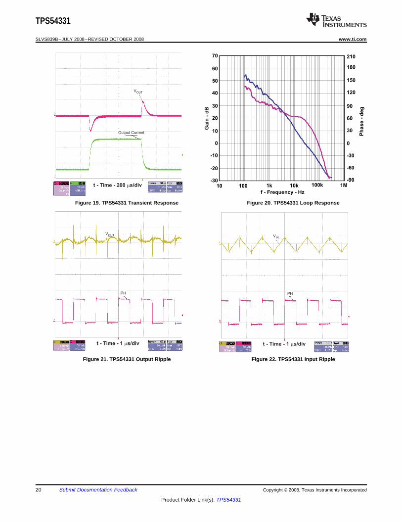
The measured overall loop response for the circuit is given in Figure 20. Note that the actual closed loopcrossover frequency is higher than intended at about 25 kHz. This is primarily due to variation in the actualvalues of the output filter components and tolerance variation of the internal feed-forward gain circuitry. Overallthe design has greater than 60 degrees of phase margin and will be completely stable over all combinations ofline and load variability.
Now that the phase loss is known the required amount of phase boost to meet the phase margin requirementcan be determined. The required phase boost is given by Equation 21:
Where PM = the desired phase margin.
A zero / pole pair of the compensation network will be placed symmetrically around the intended closed loopfrequency to provide maximum phase boost at the crossover point. The amount of separation can be determinedby Equation 22 and the resultant zero and pole frequencies are given by Equation 23 and Equation 24
The low-frequency pole is set so that the gain at the crossover frequency is equal to the inverse of the gain of themodulator and output filter. Due to the relationships established by the pole and zero relationships, the value ofRZ can be derived directly by Equation 25 :
Where:VO = Output voltageCO = Output capacitanceFCO = Desired crossover frequencyROA = 8 MΩGMCOMP = 12 A/VVggm = 800VREF = 0.8 V
With RZ known, CZ and CP can be calculated using Equation 26 and Equation 27:
14 Submit Documentation Feedback Copyright © 2008, Texas Instruments Incorporated
Product Folder Link(s): TPS54331
zZ
Z
RFC
´´´
=
12
1
p
(26)
zP
P
RFC
´´´
=
12
1
p(27)
-6 62 25000 3.3 54 10 8 10
Rz = = 29.2 k12 800 0.8
p´ ´ ´ ´ ´ ´ ´W
´ ´ (28)1
= = 928 pF2 6010 29200
Czp´ ´ ´ (29)
1= = 51 pF
2 103900 29200Cp
p´ ´ ´ (30)
BOOTSTRAP CAPACITOR
CATCH DIODE
TPS54331
www.ti.com ...................................................................................................................................................... SLVS839B–JULY 2008–REVISED OCTOBER 2008
For this design, the two 47-µF output capacitors are used. For ceramic capacitors, the actual output capacitanceis less than the rated value when the capacitors have a dc bias voltage applied. This is the case in a dc/dcconverter. The actual output capacitance may be as low as 54 µF. The combined ESR is approximately .001 Ω.
Using Equation 19 and Equation 20, the output stage gain and phase loss are equivalent as:Gain = –2.26 dBandPL - –83.52 degrees
For 70 degrees of phase margin, Equation 21 requires 63.52 degrees of phase boost.
Equation 22, Equation 23, and Equation 24 are used to find the zero and pole frequencies of:
FZ1 = 5883 Hz
And
FP1 = 106200 Hz
RZ, CZ, and CP are calculated using Equation 25, Equation 26, and Equation 27:
Using standard values for R3, C6, and C7 in the application schematic of Figure 13:
R3 = 29.4 kΩ
C6 = 1000 pF
C7 = 47 pF
Every TPS54331 design requires a bootstrap capacitor, C4. The bootstrap capacitor must be 0.1 µF. Thebootstrap capacitor is located between the PH pins and BOOT pin. The bootstrap capacitor should be ahigh-quality ceramic type with X7R or X5R grade dielectric for temperature stability.
The TPS54331 is designed to operate using an external catch diode between PH and GND. The selected diodemust meet the absolute maximum ratings for the application: Reverse voltage must be higher than the maximumvoltage at the PH pin, which is VINMAX + 0.5 V. Peak current must be greater than IOUTMAX plus on half thepeak to peak inductor current. Forward voltage drop should be small for higher efficiencies. It is important to notethat the catch diode conduction time is typically longer than the high-side FET on time, so attention paid to diodeparameters can make a marked improvement in overall efficiency. Additionally, check that the device chosen iscapable of dissipating the power losses. For this design, a Diodes, Inc. B340A is chosen, with a reverse voltageof 40 V, forward current of 3 A, and a forward voltage drop of 0.5 V.
Copyright © 2008, Texas Instruments Incorporated Submit Documentation Feedback 15
Product Folder Link(s): TPS54331
OUTPUT VOLTAGE LIMITATIONS
( )( ) ( )Omax IN min O max DSon max D O max L DV = 0.91 × V I × R + V I × R V- - - (31)
( )( ) ( )Omin IN max Omin D O min L DV = 0.089 V I Rin + V I R V´ - ´ - ´ -(32)
POWER DISSIPATION ESTIMATE
TPS54331
SLVS839B–JULY 2008–REVISED OCTOBER 2008 ...................................................................................................................................................... www.ti.com
Due to the internal design of the TPS54331, there are both upper and lower output voltage limits for any giveninput voltage. The upper limit of the output voltage set point is constrained by the maximum duty cycle of 91%and is given by Equation 31:
Where:VIN min = Minimum input voltageIO max = Maximum load currentVD = Catch diode forward voltageRL = Output inductor series resistance
The equation assumes maximum on resistance for the internal high-side FET.
The lower limit is constrained by the minimum controllable on time which may be as high as 130 ns. Theapproximate minimum output voltage for a given input voltage and minimum load current is given by Equation 32:
Where:VIN max = Maximum input voltageIO min = Minimum load currentVD = Catch diode forward voltageRL = Output inductor series resistance
This equation assumes nominal on-resistance for the high-side FET and accounts for worst case variation ofoperating frequency set point. Any design operating near the operational limits of the device should be carefullychecked to assure proper functionality.
The following formulas show how to estimate the device power dissipation under continuous conduction modeoperations. They should not be used if the device is working in the discontinuous conduction mode (DCM) orpulse skipping Eco-modeTM.
The device power dissipation includes:
1) Conduction loss: Pcon = IOUT2 x Rds(on) x VOUT/VIN
2) Switching loss: Psw = 0.5 x 10⁻⁹ x VIN2 x IOUT x Fsw
3) Gate charge loss: Pgc = 22.8 x 10⁻⁹ x Fsw
4) Quiescent current loss: Pq = 0.11 x 10⁻³ x VIN
Where:
IOUT is the output current (A).
Rds(on) is the on-resistance of the high-side MOSFET (Ω).
VOUT is the output voltage (V).
VIN is the input voltage (V).
Fsw is the switching frequency (Hz).
So
Ptot = Pcon + Psw + Pgc + Pq
For given TA , TJ = TA + Rth x Ptot.
For given TJMAX = 150°C, TAMAX = TJMAX– Rth x Ptot.
16 Submit Documentation Feedback Copyright © 2008, Texas Instruments Incorporated
Product Folder Link(s): TPS54331
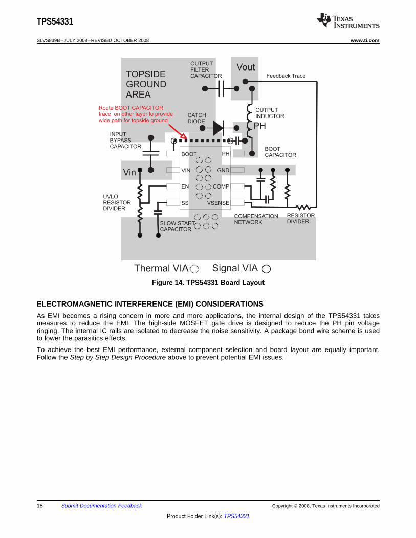
PCB LAYOUT
TPS54331
www.ti.com ...................................................................................................................................................... SLVS839B–JULY 2008–REVISED OCTOBER 2008
Where:
Ptot is the total device power dissipation (W).
TA is the ambient temperature (°C).
TJ is the junction temperature (°C) .
Rth is the thermal resistance of the package (°C/W).
TJMAX is maximum junction temperature (°C).
TAMAX is maximum ambient temperature (°C).
The VIN pin should be bypassed to ground with a low ESR ceramic bypass capacitor. Care should be taken tominimize the loop area formed by the bypass capacitor connections, the VIN pin, and the anode of the catchdiode. The typical recommended bypass capacitance is 10-µF ceramic with a X5R or X7R dielectric and theoptimum placement is closest to the VIN pins and the source of the anode of the catch diode. See Figure 14 fora PCB layout example. The GND D pin should be tied to the PCB ground plane at the pin of the IC. The sourceof the low-side MOSFET should be connected directly to the top side PCB ground area used to tie together theground sides of the input and output capacitors as well as the anode of the catch diode. The PH pin should berouted to the cathode of the catch diode and to the output inductor. Since the PH connection is the switchingnode, the catch diode and output inductor should be located very close to the PH pins, and the area of the PCBconductor minimized to prevent excessive capacitive coupling. For operation at full rated load, the top sideground area must provide adequate heat dissipating area. The TPS54331 uses a fused lead frame so that theGND pin acts as a conductive path for heat dissipation from the die. Many applications have larger areas ofinternal or back side ground plane available, and the top side ground area can be connected to these areasusing multiple vias under or adjacent to the device to help dissipate heat. The additional external componentscan be placed approximately as shown. It may be possible to obtain acceptable performance with alternatelayout schemes, however this layout has been shown to produce good results and is intended as a guideline.
Copyright © 2008, Texas Instruments Incorporated Submit Documentation Feedback 17
Product Folder Link(s): TPS54331
BOOT
VSENSE
PH
VIN GND
EN
Vout
PH
Vin
TOPSIDEGROUNDAREA
OUTPUTINDUCTOR
OUTPUTFILTERCAPACITOR
BOOTCAPACITOR
INPUTBYPASSCAPACITOR
CATCHDIODE
Signal VIA
Route BOOT CAPACITORtrace on other layer to providewide path for topside ground
RESISTORDIVIDER
Feedback Trace
COMP
SS
COMPENSATIONNETWORK
Thermal VIA
SLOW STARTCAPACITOR
UVLORESISTORDIVIDER
ELECTROMAGNETIC INTERFERENCE (EMI) CONSIDERATIONS
TPS54331
SLVS839B–JULY 2008–REVISED OCTOBER 2008 ...................................................................................................................................................... www.ti.com
Figure 14. TPS54331 Board Layout
As EMI becomes a rising concern in more and more applications, the internal design of the TPS54331 takesmeasures to reduce the EMI. The high-side MOSFET gate drive is designed to reduce the PH pin voltageringing. The internal IC rails are isolated to decrease the noise sensitivity. A package bond wire scheme is usedto lower the parasitics effects.
To achieve the best EMI performance, external component selection and board layout are equally important.Follow the Step by Step Design Procedure above to prevent potential EMI issues.
18 Submit Documentation Feedback Copyright © 2008, Texas Instruments Incorporated
Product Folder Link(s): TPS54331
APPLICATION CURVES
0
10
20
30
40
50
60
70
80
90
100
0 0.02 0.04 0.06 0.08 0.1 0.12 0.14 0.16 0.18 0.2
I - Output Current - AO
Eff
icie
nc
y -
%
V = 7 VIN V = 14 VIN
V = 21 VINV = 28 VIN
0
10
20
30
40
50
60
70
80
90
100
0 0.5 1 1.5 2 2.5 3
I - Output Current - AO
Eff
icie
nc
y -
%
V = 7 VIN
V = 14 VINV = 21 VINV = 28 VIN
0.9985
0.999
0.9995
1
1.0005
1.001
1.0015
1.002
1.0025
1.003
1.0035
1.004
0 0.5 1 1.5 2 2.5 3 3.5
V = 14 VIN
V = 21 VIN
V = 28 VIN
V = 7 VIN
I - Output Current - AO
Ou
tpu
t R
eg
ula
tio
n -
%
VO
utp
ut
Vo
lta
ge
- V
O-
3.28
3.29
3.3
3.31
3.32
3.33
3.34
3.35
3.36
3.37
3.38
0 5 10 15 20 25 30
V - Input Voltage -VI
I = 0 AO
I = 1.5 AO
I = 3 AO
TPS54331
www.ti.com ...................................................................................................................................................... SLVS839B–JULY 2008–REVISED OCTOBER 2008
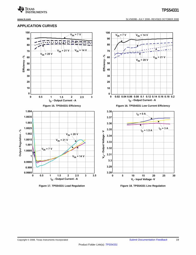
Figure 15. TPS54331 Efficiency Figure 16. TPS54331 Low Current Efficiency
Figure 17. TPS54331 Load Regulation Figure 18. TPS54331 Line Regulation
Copyright © 2008, Texas Instruments Incorporated Submit Documentation Feedback 19
Product Folder Link(s): TPS54331
-30
-20
-10
0
10
20
30
40
50
60
70
f - Frequency - Hz
-90
-60
-30
0
30
60
90
120
150
180
210
Ph
ase -
deg
10 100 1k 10k 100k 1M
Gain
- d
B
VOUT
Output Current
t - Time - 200 s/divm
VOUT
PH
t - Time - 1 s/divm
VIN
PH
t - Time - 1 s/divm
TPS54331
SLVS839B–JULY 2008–REVISED OCTOBER 2008 ...................................................................................................................................................... www.ti.com
Figure 19. TPS54331 Transient Response Figure 20. TPS54331 Loop Response
Figure 21. TPS54331 Output Ripple Figure 22. TPS54331 Input Ripple
20 Submit Documentation Feedback Copyright © 2008, Texas Instruments Incorporated
Product Folder Link(s): TPS54331
VIN
VOUT
t - Time - 5 ms/div
ENA
VOUT
t - Time - 5 ms/div
TPS54331
www.ti.com ...................................................................................................................................................... SLVS839B–JULY 2008–REVISED OCTOBER 2008
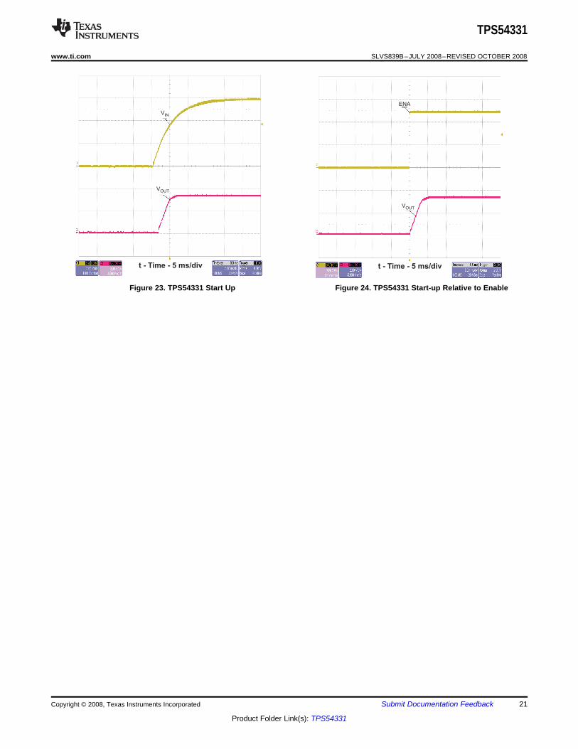
Figure 23. TPS54331 Start Up Figure 24. TPS54331 Start-up Relative to Enable
Copyright © 2008, Texas Instruments Incorporated Submit Documentation Feedback 21
Product Folder Link(s): TPS54331
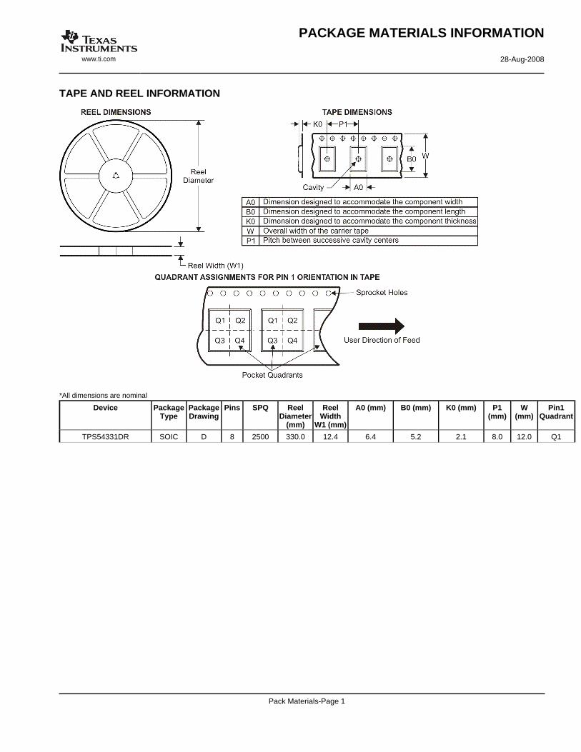
TAPE AND REEL INFORMATION
*All dimensions are nominal
Device PackageType
PackageDrawing
Pins SPQ ReelDiameter
(mm)
ReelWidth
W1 (mm)
A0 (mm) B0 (mm) K0 (mm) P1(mm)
W(mm)
Pin1Quadrant
TPS54331DR SOIC D 8 2500 330.0 12.4 6.4 5.2 2.1 8.0 12.0 Q1
PACKAGE MATERIALS INFORMATION
www.ti.com 28-Aug-2008
Pack Materials-Page 1
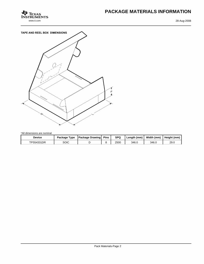
*All dimensions are nominal
Device Package Type Package Drawing Pins SPQ Length (mm) Width (mm) Height (mm)
TPS54331DR SOIC D 8 2500 346.0 346.0 29.0
PACKAGE MATERIALS INFORMATION
www.ti.com 28-Aug-2008
Pack Materials-Page 2
IMPORTANT NOTICETexas Instruments Incorporated and its subsidiaries (TI) reserve the right to make corrections, modifications, enhancements, improvements,and other changes to its products and services at any time and to discontinue any product or service without notice. Customers shouldobtain the latest relevant information before placing orders and should verify that such information is current and complete. All products aresold subject to TI’s terms and conditions of sale supplied at the time of order acknowledgment.TI warrants performance of its hardware products to the specifications applicable at the time of sale in accordance with TI’s standardwarranty. Testing and other quality control techniques are used to the extent TI deems necessary to support this warranty. Except wheremandated by government requirements, testing of all parameters of each product is not necessarily performed.TI assumes no liability for applications assistance or customer product design. Customers are responsible for their products andapplications using TI components. To minimize the risks associated with customer products and applications, customers should provideadequate design and operating safeguards.TI does not warrant or represent that any license, either express or implied, is granted under any TI patent right, copyright, mask work right,or other TI intellectual property right relating to any combination, machine, or process in which TI products or services are used. Informationpublished by TI regarding third-party products or services does not constitute a license from TI to use such products or services or awarranty or endorsement thereof. Use of such information may require a license from a third party under the patents or other intellectualproperty of the third party, or a license from TI under the patents or other intellectual property of TI.Reproduction of TI information in TI data books or data sheets is permissible only if reproduction is without alteration and is accompaniedby all associated warranties, conditions, limitations, and notices. Reproduction of this information with alteration is an unfair and deceptivebusiness practice. TI is not responsible or liable for such altered documentation. Information of third parties may be subject to additionalrestrictions.Resale of TI products or services with statements different from or beyond the parameters stated by TI for that product or service voids allexpress and any implied warranties for the associated TI product or service and is an unfair and deceptive business practice. TI is notresponsible or liable for any such statements.TI products are not authorized for use in safety-critical applications (such as life support) where a failure of the TI product would reasonablybe expected to cause severe personal injury or death, unless officers of the parties have executed an agreement specifically governingsuch use. Buyers represent that they have all necessary expertise in the safety and regulatory ramifications of their applications, andacknowledge and agree that they are solely responsible for all legal, regulatory and safety-related requirements concerning their productsand any use of TI products in such safety-critical applications, notwithstanding any applications-related information or support that may beprovided by TI. Further, Buyers must fully indemnify TI and its representatives against any damages arising out of the use of TI products insuch safety-critical applications.TI products are neither designed nor intended for use in military/aerospace applications or environments unless the TI products arespecifically designated by TI as military-grade or "enhanced plastic." Only products designated by TI as military-grade meet militaryspecifications. Buyers acknowledge and agree that any such use of TI products which TI has not designated as military-grade is solely atthe Buyer's risk, and that they are solely responsible for compliance with all legal and regulatory requirements in connection with such use.TI products are neither designed nor intended for use in automotive applications or environments unless the specific TI products aredesignated by TI as compliant with ISO/TS 16949 requirements. Buyers acknowledge and agree that, if they use any non-designatedproducts in automotive applications, TI will not be responsible for any failure to meet such requirements.Following are URLs where you can obtain information on other Texas Instruments products and application solutions:Products ApplicationsAmplifiers amplifier.ti.com Audio www.ti.com/audioData Converters dataconverter.ti.com Automotive www.ti.com/automotiveDSP dsp.ti.com Broadband www.ti.com/broadbandClocks and Timers www.ti.com/clocks Digital Control www.ti.com/digitalcontrolInterface interface.ti.com Medical www.ti.com/medicalLogic logic.ti.com Military www.ti.com/militaryPower Mgmt power.ti.com Optical Networking www.ti.com/opticalnetworkMicrocontrollers microcontroller.ti.com Security www.ti.com/securityRFID www.ti-rfid.com Telephony www.ti.com/telephonyRF/IF and ZigBee® Solutions www.ti.com/lprf Video & Imaging www.ti.com/video
Wireless www.ti.com/wireless
Mailing Address: Texas Instruments, Post Office Box 655303, Dallas, Texas 75265Copyright © 2008, Texas Instruments Incorporated