Embed Size (px)
Citation preview

Merging 3D printing with optical and CT-Scan imaging systemsfor re-creating PCBs
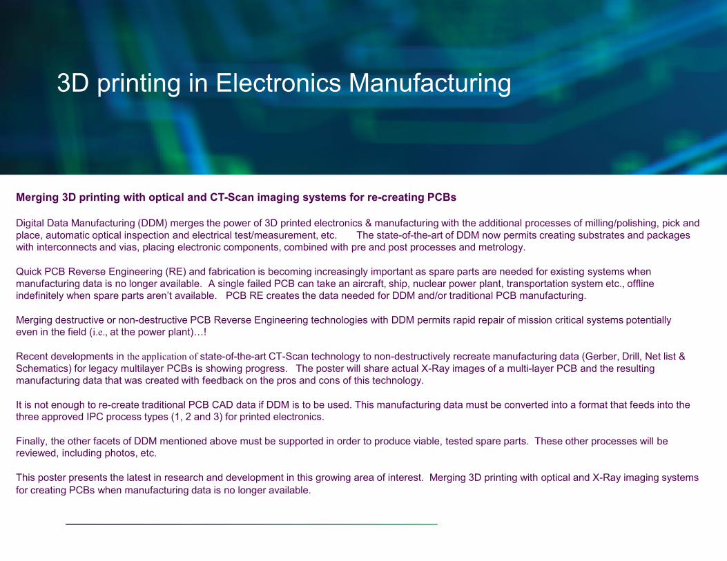
Merging 3D printing with optical and CT-Scan imaging systems for re-creating PCBs
Digital Data Manufacturing (DDM) merges the power of 3D printed electronics & manufacturing with the additional processes of milling/polishing, pick and place, automatic optical inspection and electrical test/measurement, etc. The state-of-the-art of DDM now permits creating substrates and packages with interconnects and vias, placing electronic components, combined with pre and post processes and metrology.
Quick PCB Reverse Engineering (RE) and fabrication is becoming increasingly important as spare parts are needed for existing systems when manufacturing data is no longer available. A single failed PCB can take an aircraft, ship, nuclear power plant, transportation system etc., offline indefinitely when spare parts aren’t available. PCB RE creates the data needed for DDM and/or traditional PCB manufacturing.
Merging destructive or non-destructive PCB Reverse Engineering technologies with DDM permits rapid repair of mission critical systems potentially even in the field (i.e., at the power plant)…!
Recent developments in the application of state-of-the-art CT-Scan technology to non-destructively recreate manufacturing data (Gerber, Drill, Net list & Schematics) for legacy multilayer PCBs is showing progress. The poster will share actual X-Ray images of a multi-layer PCB and the resulting manufacturing data that was created with feedback on the pros and cons of this technology.
It is not enough to re-create traditional PCB CAD data if DDM is to be used. This manufacturing data must be converted into a format that feeds into the three approved IPC process types (1, 2 and 3) for printed electronics.
Finally, the other facets of DDM mentioned above must be supported in order to produce viable, tested spare parts. These other processes will be reviewed, including photos, etc.
This poster presents the latest in research and development in this growing area of interest. Merging 3D printing with optical and X-Ray imaging systems for creating PCBs when manufacturing data is no longer available.
3D printing in Electronics Manufacturing
INTRODUCTION
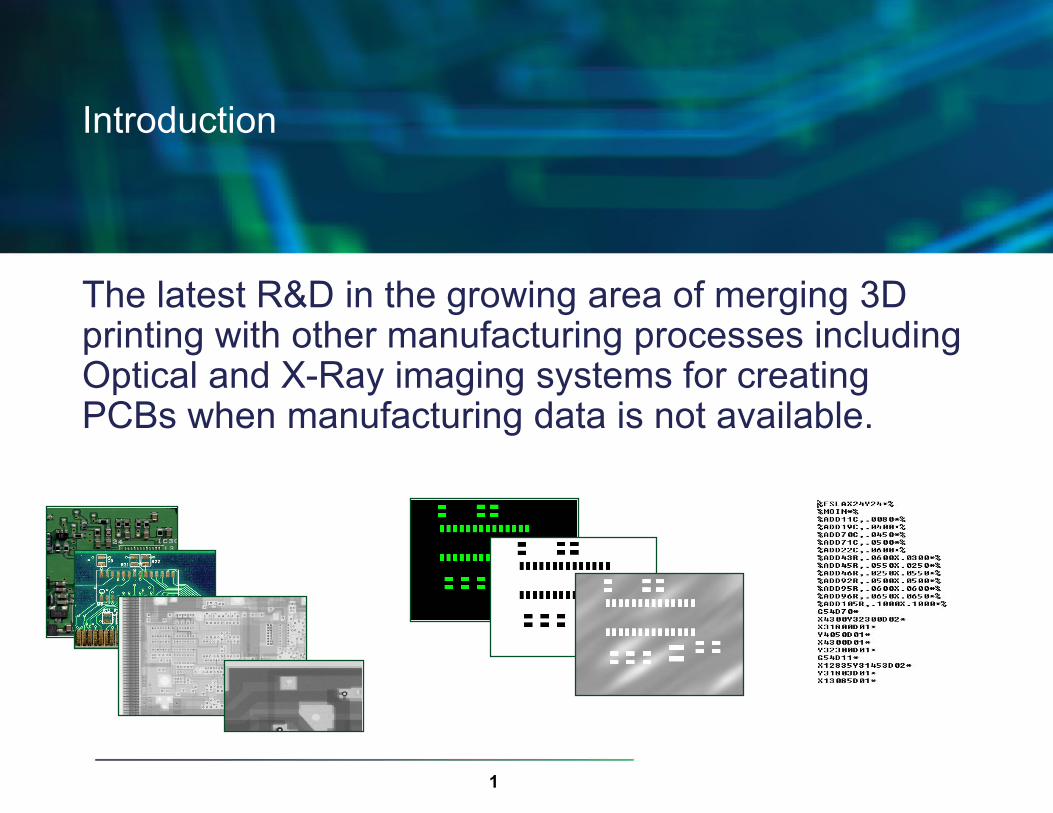
The latest R&D in the growing area of merging 3D printing with other manufacturing processes including Optical and X-Ray imaging systems for creating PCBs when manufacturing data is not available.
1
Introduction
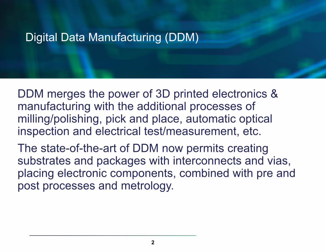
Digital Data Manufacturing (DDM)
DDM merges the power of 3D printed electronics & manufacturing with the additional processes of milling/polishing, pick and place, automatic optical inspection and electrical test/measurement, etc.The state-of-the-art of DDM now permits creating substrates and packages with interconnects and vias, placing electronic components, combined with pre and post processes and metrology.
2
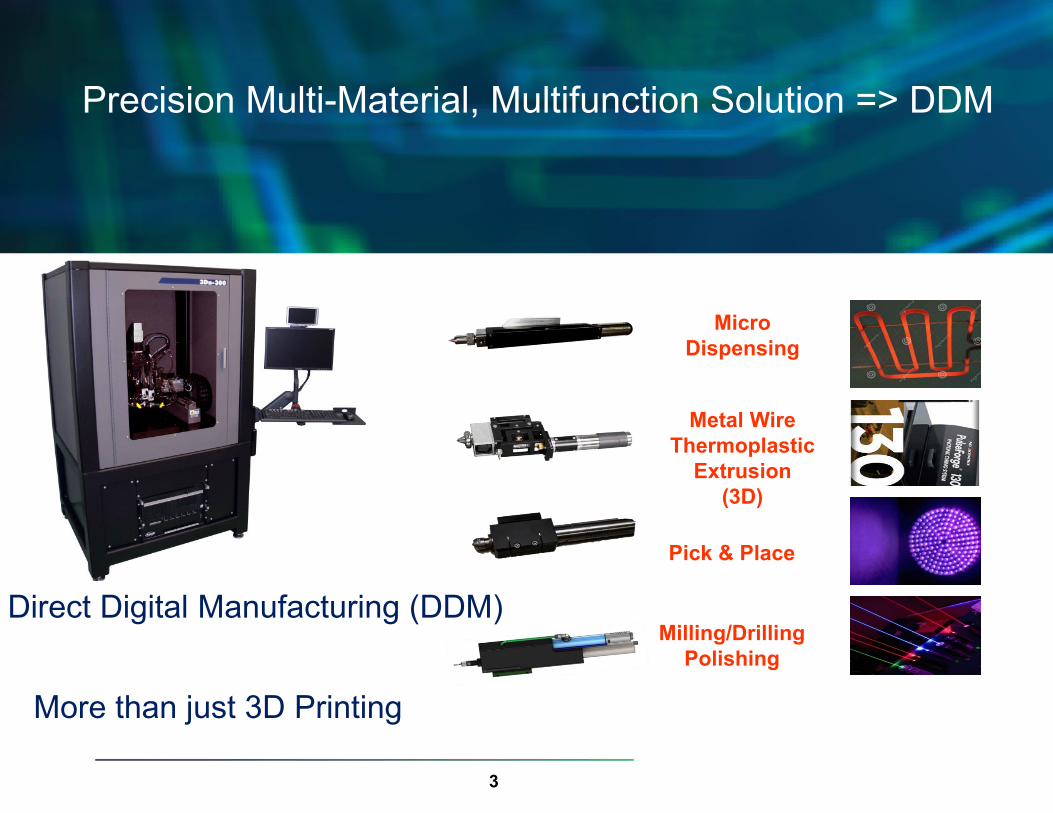
Precision Multi-Material, Multifunction Solution => DDM
3
Direct Digital Manufacturing (DDM)
More than just 3D Printing
MicroDispensing
Pick & Place
Metal WireThermoplastic
Extrusion(3D)
Milling/DrillingPolishing
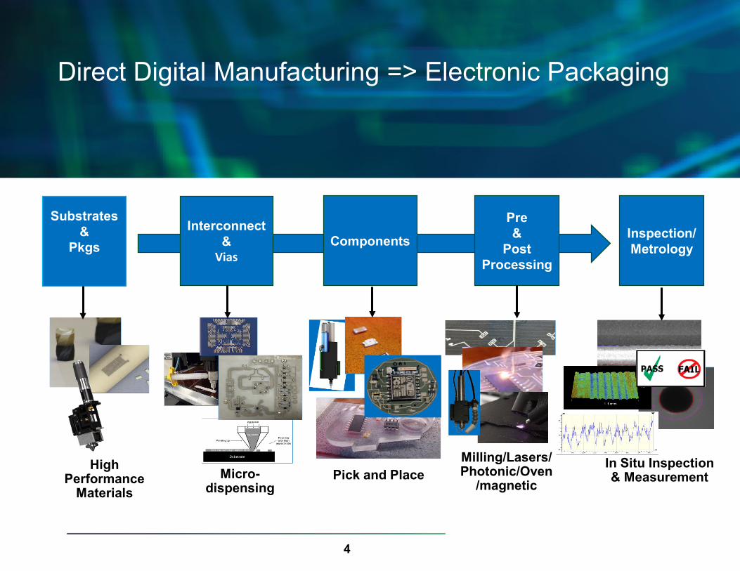
Direct Digital Manufacturing => Electronic Packaging
4
Interconnect&
ViasComponents
Pre&
PostProcessing
Inspection/Metrology
Substrates&
Pkgs
Micro-dispensing
High Performance
MaterialsPick and Place
Milling/Lasers/Photonic/Oven
/magneticIn Situ Inspection & Measurement

What if required data is not available for DDM…?
PCB Reverse Engineering (RE) provides the data
Quick PCB Reverse Engineering (RE) and fabrication/repair is becoming increasingly important as spare parts are needed for existing systems when manufacturing data isn’t available. A single failed PCB can take an aircraft, ship, nuclear power plant, transportation system, etc. offline indefinitely when spare parts aren’t available. PCB RE creates the data required for DDM and/or traditional PCB manufacturing.
5
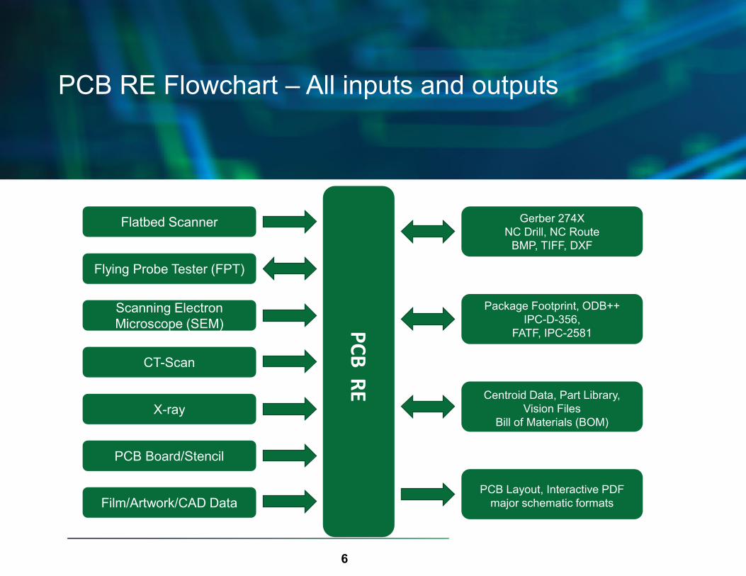
PCB RE Flowchart – All inputs and outputs
6
Flatbed Scanner
Flying Probe Tester (FPT)
Scanning Electron Microscope (SEM)
CT-Scan
X-ray
PCB Board/Stencil
Film/Artwork/CAD Data
Gerber 274XNC Drill, NC Route
BMP, TIFF, DXF
Package Footprint, ODB++IPC-D-356,
FATF, IPC-2581
Centroid Data, Part Library, Vision Files
Bill of Materials (BOM)
PCB Layout, Interactive PDFmajor schematic formats
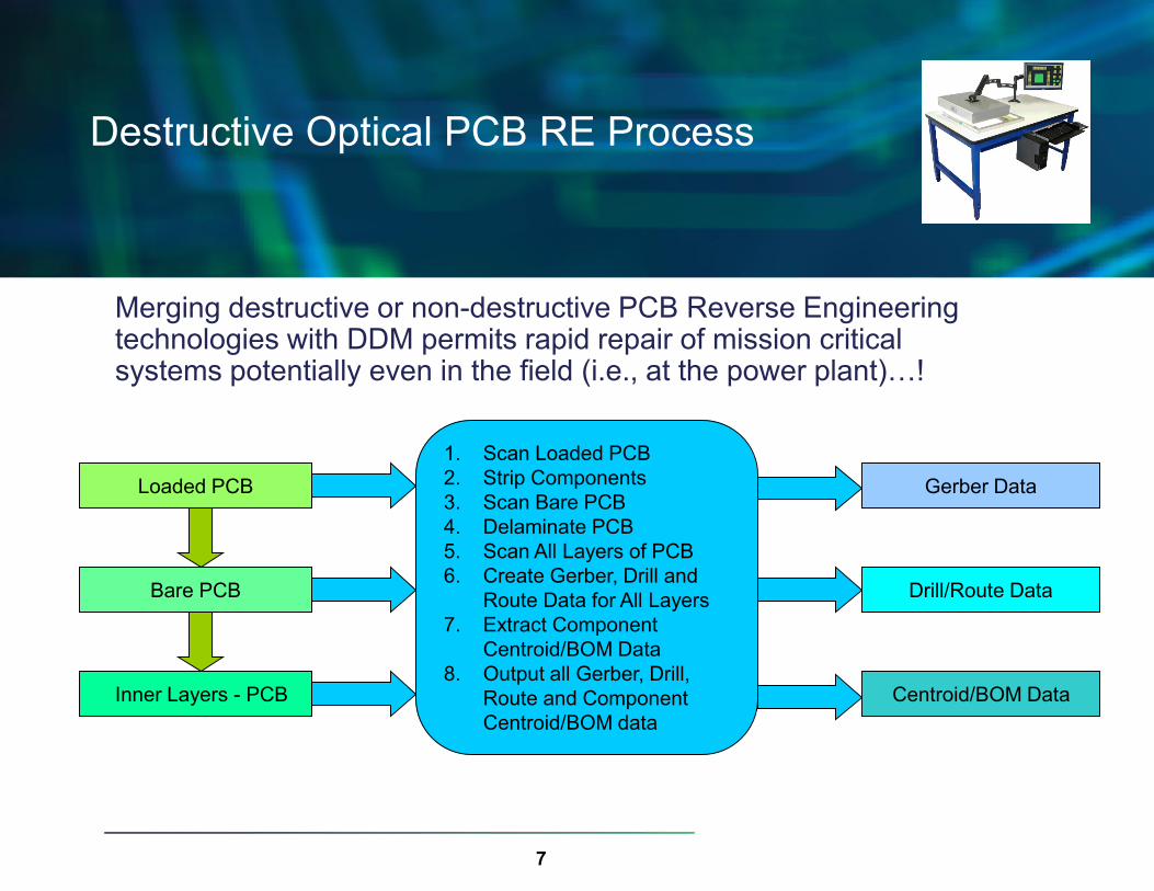
Destructive Optical PCB RE Process
Merging destructive or non-destructive PCB Reverse Engineering technologies with DDM permits rapid repair of mission critical systems potentially even in the field (i.e., at the power plant)…!
7
Loaded PCB
Bare PCB
Inner Layers - PCB
1. Scan Loaded PCB2. Strip Components3. Scan Bare PCB4. Delaminate PCB5. Scan All Layers of PCB6. Create Gerber, Drill and
Route Data for All Layers7. Extract Component
Centroid/BOM Data8. Output all Gerber, Drill,
Route and Component Centroid/BOM data
Gerber Data
Drill/Route Data
Centroid/BOM Data
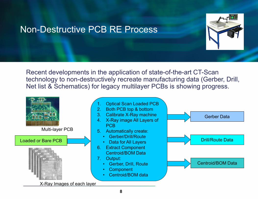
Non-Destructive PCB RE Process
Recent developments in the application of state-of-the-art CT-Scan technology to non-destructively recreate manufacturing data (Gerber, Drill, Net list & Schematics) for legacy multilayer PCBs is showing progress.
8X-Ray Images of each layer
Loaded or Bare PCB
1. Optical Scan Loaded PCB2. Both PCB top & bottom3. Calibrate X-Ray machine4. X-Ray image All Layers of
PCB5. Automatically create:
• Gerber/Drill/Route • Data for All Layers
6. Extract Component Centroid/BOM Data
7. Output: • Gerber, Drill, Route• Component• Centroid/BOM data
Gerber Data
Drill/Route Data
Centroid/BOM Data
Multi-layer PCB
Data Conversion and Process Types
It is not enough to re-create traditional PCB CAD data if DDM is to be used. This manufacturing data must be converted into a format that feeds into the three approved IPC process types (1, 2 and 3) for printed electronics.
9
• IPC Process Types - Three types of 3D printed electronics processes were approved:
• Type 1 -- Using printed electronics processes on a planar substrate • Type 2 -- Using printed electronics processes on a nonplanar substrate • Type 3 -- Using printed electronics processes to fully build and
functionalize a device in a 3D space (no starting substrate)
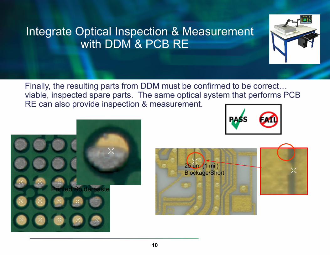
Integrate Optical Inspection & Measurement with DDM & PCB RE
Finally, the resulting parts from DDM must be confirmed to be correct… viable, inspected spare parts. The same optical system that performs PCB RE can also provide inspection & measurement.
10
25 um (1 mil) Blockage/Short
Printed Solderpaste
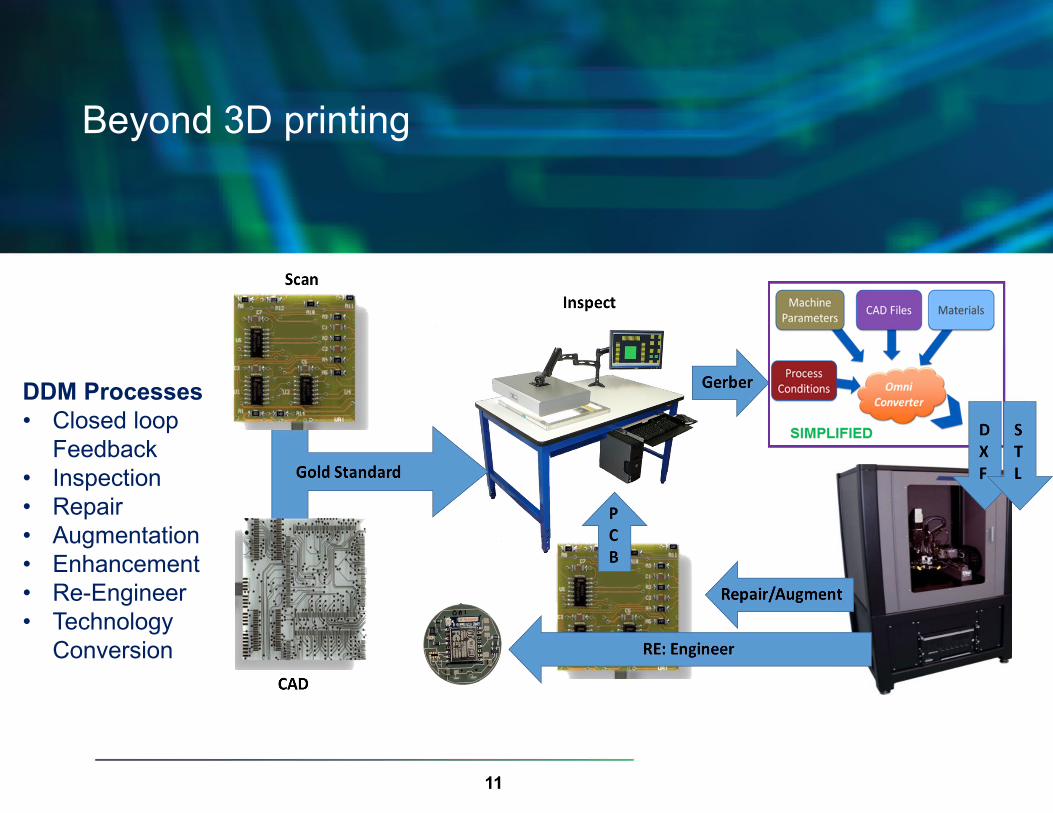
Beyond 3D printing
11
DDM Processes• Closed loop
Feedback• Inspection• Repair• Augmentation• Enhancement• Re-Engineer• Technology
Conversion

12
- PCB Re-Engineering- Micro-dispensing- Micro-spraying- Micro-milling- Digital Polishing- Pick and place- Post processing- Measurement &
Inspection- In situ monitoring
Summary: A Factory in a Tool… in the field!