Embed Size (px)
Citation preview
© 2007 Copyrights © Yole Développement SARL. All rights reserved.
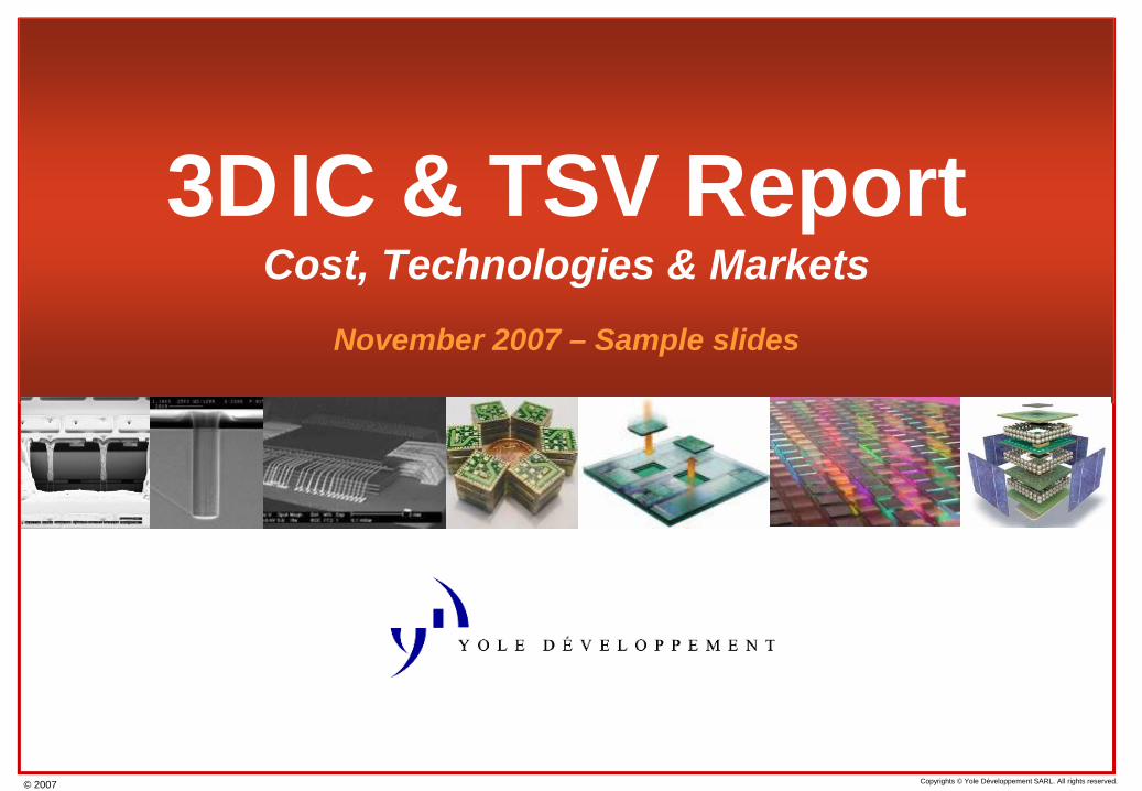
3DIC & TSV ReportCost, Technologies & Markets
November 2007 – Sample slides
© 2007 • 2Copyrights © Yole Développement SARL. All rights reserved.
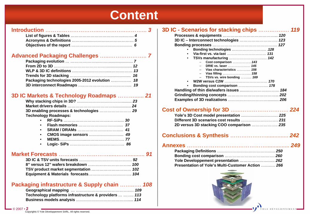
ContentIntroduction ………………………...…………..………... 3
List of figures & Tables …………………………………..……. 4Acronyms & Definitions …………..…………………………… 5Objectives of the report ………………………………………. 6
Advanced Packaging Challenges …...……………….. 7Packaging evolution … ………….……....….…...................... 7From 2D to 3D ……………………………….…....................... 12WLP & 3D IC definitions ….……….………….....…….……… 13Trends for 3D stacking …….….………………..................... 16Packaging technologies 2005-2012 evolution …..……….. 183D interconnect Roadmaps …..……………………………... 19
3D IC Markets & Technology Roadmaps ………...... 21Why stacking chips in 3D? ………………….…………......... 23Market drivers details ………………….…………................. 243D enabling processes & technologies …………………… 29Technology Roadmaps:
• RF-SiPs ……………………………..……...... 30• Flash memories ……………….…….…...... 37• SRAM / DRAMs ……………….…..……...... 41• CMOS image sensors ……….…….…….... 49• MEMS………………...……………………….. 77• Logic- SiPs ………………..…………..…….. 86
Market Forecasts ……………………….....……........... 913D IC & TSV units forecasts ……………………………….… 928” versus 12” wafers breakdown …………………………... 100TSV product market segmentation ………………………… 102Equipment & Materials forecasts…………………….…….. 104
Packaging infrastructure & Supply chain ……..…. 108Geographical mapping … …………………………………..… 109Technology platforms infrastructure & providers … …….. 113Business models analysis …………………………………..... 114
3D IC - Scenarios for stacking chips ………….…. 119Processes & equipments …………………………………... 1203D IC – Interconnect technologies ……………………….. 123Bonding processes …………………………………………. 127
• Bonding technologies ……………………….. .128• Via-first vs. via-last …………………………… 131• TSVs manufacturing ………………………..… 142
– Cost comparison ………………143– DRIE vs. laser ………………… 145– Vias characteristics …………. 156– Vias filling ……………………... 158– TSVs vs. wire bonding ……..... 169
• W2W versus C2W ……………………………… 170• Bonding cost comparison ……………………. 178
Handling of thin die/wafers issues .........…………..……... 184Grinding/thinning concepts ………………………………... 202Examples of 3D realizations ………………………….......... 206
Cost of Ownership for 3D …...…………………….. 224Yole’s 3D Cost model presentation …………….………… 225Different 3D scenarios cost results ………………………. 2312D versus 3D stacking COO comparison ……………….. 235
Conclusions & Synthesis …………….…............... 242
Annexes ……………………….……………............... 249Packaging Definitions ………………………………….…. 250Bonding cost comparison ………………………….……. 260Yole Developpement presentation ………………….….. 262Presentation of Yole’s Multi-Customer Action ……..… 266
© 2007 • 3Copyrights © Yole Développement SARL. All rights reserved.
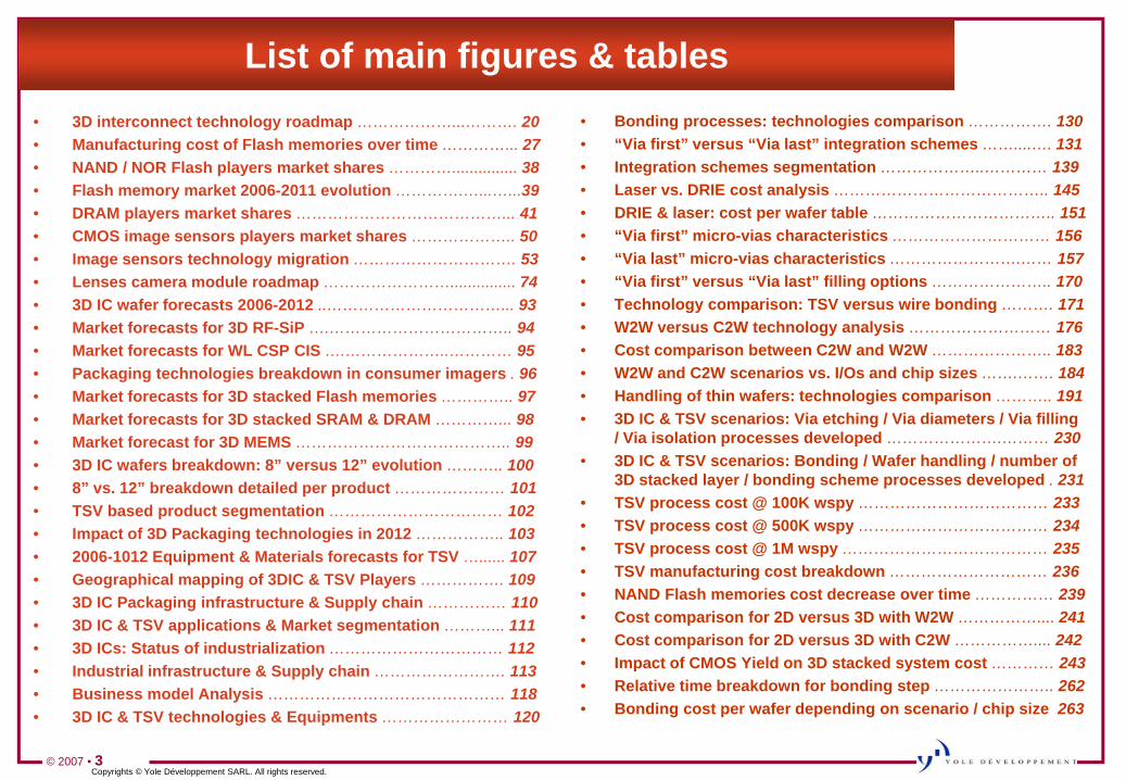
List of main figures & tables• 3D interconnect technology roadmap ………………...………. 20• Manufacturing cost of Flash memories over time …………... 27• NAND / NOR Flash players market shares …………............... 38• Flash memory market 2006-2011 evolution ………….…...…...39• DRAM players market shares …………………………………... 41• CMOS image sensors players market shares ……………….. 50• Image sensors technology migration …………………………. 53• Lenses camera module roadmap ……………………............... 74• 3D IC wafer forecasts 2006-2012 ..……………………………... 93• Market forecasts for 3D RF-SiP ….…………………………….. 94• Market forecasts for WL CSP CIS ….………………..………… 95• Packaging technologies breakdown in consumer imagers . 96• Market forecasts for 3D stacked Flash memories ………….. 97• Market forecasts for 3D stacked SRAM & DRAM …………... 98• Market forecast for 3D MEMS ………………………………….. 99• 3D IC wafers breakdown: 8” versus 12” evolution ……….. 100• 8” vs. 12” breakdown detailed per product ………………… 101• TSV based product segmentation …………………………… 102• Impact of 3D Packaging technologies in 2012 …………….. 103• 2006-1012 Equipment & Materials forecasts for TSV …...... 107• Geographical mapping of 3DIC & TSV Players ……………. 109• 3D IC Packaging infrastructure & Supply chain …………… 110• 3D IC & TSV applications & Market segmentation ………... 111• 3D ICs: Status of industrialization …………………………… 112• Industrial infrastructure & Supply chain ……………………. 113• Business model Analysis ……………………………………… 118• 3D IC & TSV technologies & Equipments …………………… 120
• Bonding processes: technologies comparison ……………. 130• “Via first” versus “Via last” integration schemes ……....…. 131• Integration schemes segmentation ………………..………… 139• Laser vs. DRIE cost analysis ………………………………….. 145• DRIE & laser: cost per wafer table …………………………….. 151• “Via first” micro-vias characteristics ………………………… 156• “Via last” micro-vias characteristics …………………….…… 157• “Via first” versus “Via last” filling options ………………….. 170• Technology comparison: TSV versus wire bonding ………. 171• W2W versus C2W technology analysis ……………………… 176• Cost comparison between C2W and W2W ………………….. 183• W2W and C2W scenarios vs. I/Os and chip sizes …….……. 184• Handling of thin wafers: technologies comparison ……….. 191• 3D IC & TSV scenarios: Via etching / Via diameters / Via filling
/ Via isolation processes developed ………………….……… 230• 3D IC & TSV scenarios: Bonding / Wafer handling / number of
3D stacked layer / bonding scheme processes developed . 231• TSV process cost @ 100K wspy ……………………………… 233• TSV process cost @ 500K wspy ……………………………… 234• TSV process cost @ 1M wspy ………………………………… 235• TSV manufacturing cost breakdown ………………………… 236• NAND Flash memories cost decrease over time …………… 239• Cost comparison for 2D versus 3D with W2W …………….... 241• Cost comparison for 2D versus 3D with C2W …………….... 242• Impact of CMOS Yield on 3D stacked system cost ………… 243• Relative time breakdown for bonding step ………………….. 262• Bonding cost per wafer depending on scenario / chip size 263
© 2007 • 4Copyrights © Yole Développement SARL. All rights reserved.
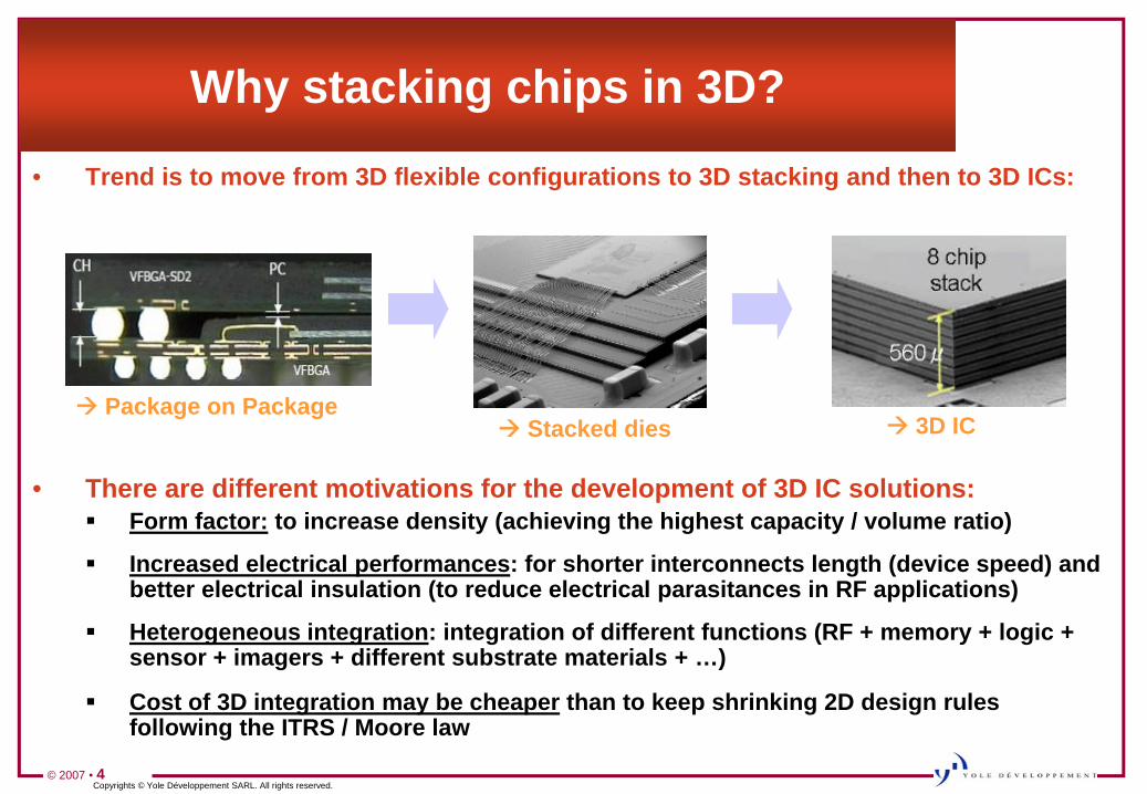
Why stacking chips in 3D?
• Trend is to move from 3D flexible configurations to 3D stacking and then to 3D ICs:
• There are different motivations for the development of 3D IC solutions:Form factor: to increase density (achieving the highest capacity / volume ratio)
Increased electrical performances: for shorter interconnects length (device speed) and better electrical insulation (to reduce electrical parasitances in RF applications)
Heterogeneous integration: integration of different functions (RF + memory + logic + sensor + imagers + different substrate materials + …)
Cost of 3D integration may be cheaper than to keep shrinking 2D design rules following the ITRS / Moore law
Stacked dies 3D ICPackage on Package
© 2007 • 5Copyrights © Yole Développement SARL. All rights reserved.
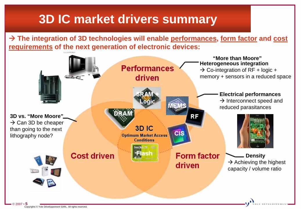
3D IC market drivers summary
Heterogeneous integration Co-integration of RF + logic +
memory + sensors in a reduced space
Electrical performances Interconnect speed and
reduced parasitances
The integration of 3D technologies will enable performances, form factor and cost requirements of the next generation of electronic devices:
Density Achieving the highest
capacity / volume ratio
3D vs. “More Moore” Can 3D be cheaper
than going to the next lithography node?
“More than Moore”
© 2007 • 6Copyrights © Yole Développement SARL. All rights reserved.
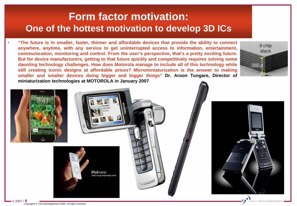
Form factor motivation:One of the hottest motivation to develop 3D ICs
• “The future is in smaller, faster, thinner and affordable devices that provide the ability to connectanywhere, anytime, with any service to get uninterrupted access to information, entertainment,communication, monitoring and control. From the user’s perspective, that’s a pretty exciting future.But for device manufacturers, getting to that future quickly and competitively requires solving somedaunting technology challenges. How does Motorola manage to include all of this technology whilestill creating iconic designs at affordable prices? Microminiaturization is the answer to makingsmaller and smaller devices doing bigger and bigger things” Dr. Aroon Tungare, Director ofminiaturization technologies at MOTOROLA in January 2007
© 2007 • 7Copyrights © Yole Développement SARL. All rights reserved.
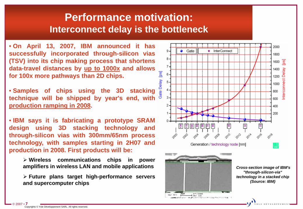
Performance motivation:Interconnect delay is the bottleneck
• On April 13, 2007, IBM announced it hassuccessfully incorporated through-silicon vias(TSV) into its chip making process that shortensdata-travel distances by up to 1000x and allowsfor 100x more pathways than 2D chips.
• Samples of chips using the 3D stackingtechnique will be shipped by year's end, withproduction ramping in 2008.
• IBM says it is fabricating a prototype SRAMdesign using 3D stacking technology andthrough-silicon vias with 300mm/65nm processtechnology, with samples starting in 2H07 andproduction in 2008. First products will be:
Wireless communications chips in poweramplifiers in wireless LAN and mobile applications
Future plans target high-performance serversand supercomputer chips
Cross-section image of IBM's "through-silicon-via“
technology in a stacked chip (Source: IBM)
© 2007 • 8Copyrights © Yole Développement SARL. All rights reserved.
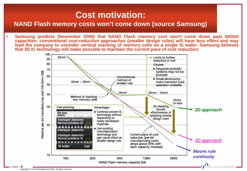
Cost motivation:NAND Flash memory costs won’t come down (source Samsung)
• Samsung predicts (November 2006) that NAND Flash memory cost won’t come down past 64Gbitcapacities: conventional cost-reduction approaches (smaller design rules) will have less effect and maylead the company to consider vertical stacking of memory cells on a single Si wafer. Samsung believesthat 3D IC technology will make possible to maintain the current pace of cost reduction:
2D approach
3D approach
Moore rule continuity
© 2007 • 9Copyrights © Yole Développement SARL. All rights reserved.
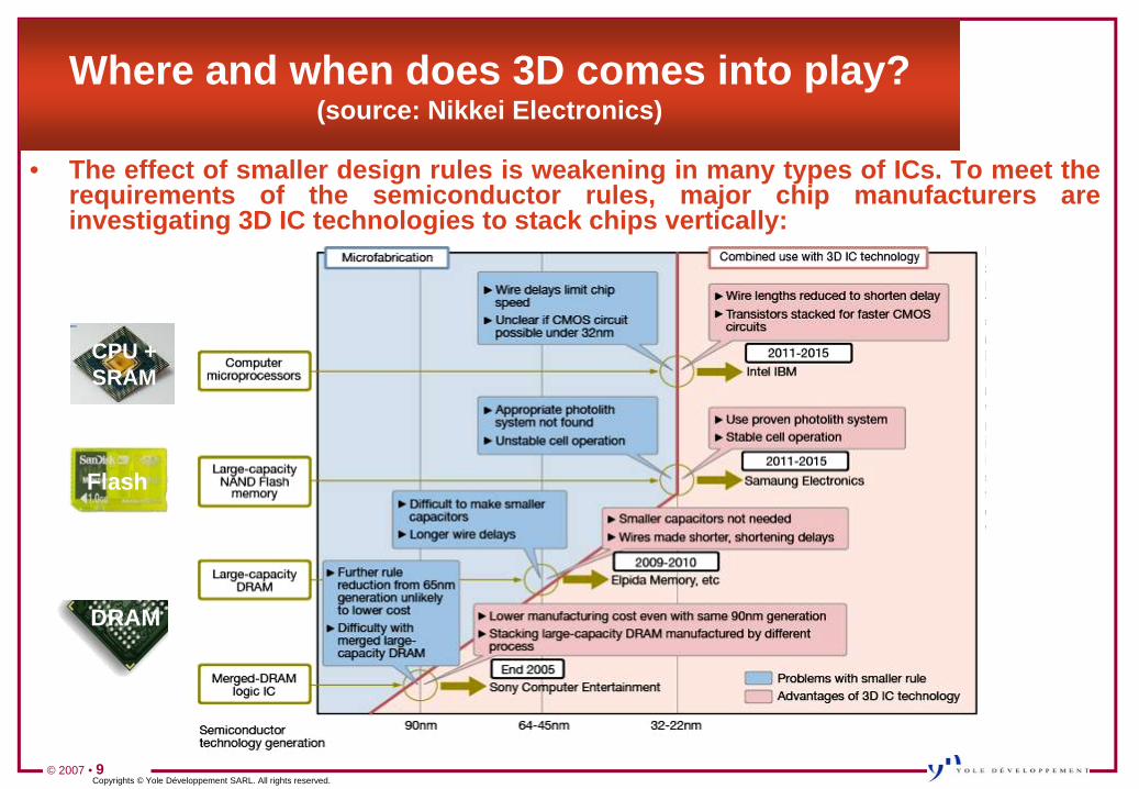
Where and when does 3D comes into play?(source: Nikkei Electronics)
• The effect of smaller design rules is weakening in many types of ICs. To meet therequirements of the semiconductor rules, major chip manufacturers areinvestigating 3D IC technologies to stack chips vertically:
CPU + SRAM
DRAM
Flash
© 2007 • 10Copyrights © Yole Développement SARL. All rights reserved.
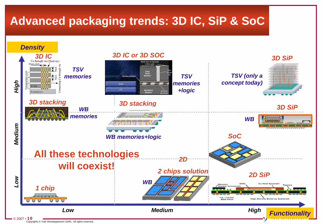
Advanced packaging trends: 3D IC, SiP & SoC
Density
Functionality
3D IC or 3D SOC 3D SiP
Low Medium High
3D IC
TSV memories
3D stackingWB
memories
Low
Med
ium
Hig
h
TSV memories
+logic
3D stacking
WB memories+logic SoC
TSV (only a concept today)
2D SiP
2D
2 chips solutionWB
1 chip
3D SiP
WB
All these technologies will coexist!
© 2007 • 11Copyrights © Yole Développement SARL. All rights reserved.
3D IC technologies and equipmentsVia drilling
Laser drilling
DRIE
Photolithography
Via filling
Electroplating
CVD
Photolithography
Wafer/Chip bonding
Adhesive, fusion oxide or metal-metal bonding
Chip alignment
Thinning
Grinding (BG)
CMP
Wet etching
Plasma etching
Laser OR
DRIE equipment
Coater
Mask aligner OR stepper
Metal deposition system
Coater
Mask aligner OR stepper
Flip Chip
Bonder
Adhesive, fusion oxide or metal-metal bonding
Wafer alignment
Wafer bonder
Wafer aligner
C2W W2W
Thinning equipments
Technologies
Equipments
Temporary bonding
equipments
© 2007 • 12Copyrights © Yole Développement SARL. All rights reserved.
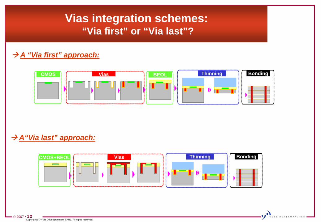
Vias integration schemes:“Via first” or “Via last”?
A “Via first” approach:
A“Via last” approach:
ThinningCMOS Vias BondingBEOL
ThinningCMOS+BEOL Vias Bonding
© 2007 • 13Copyrights © Yole Développement SARL. All rights reserved.
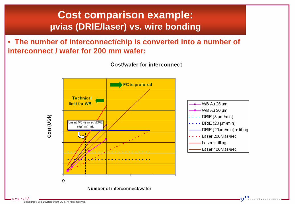
Cost comparison example:µvias (DRIE/laser) vs. wire bonding
• The number of interconnect/chip is converted into a number of interconnect / wafer for 200 mm wafer:
© 2007 • 14Copyrights © Yole Développement SARL. All rights reserved.
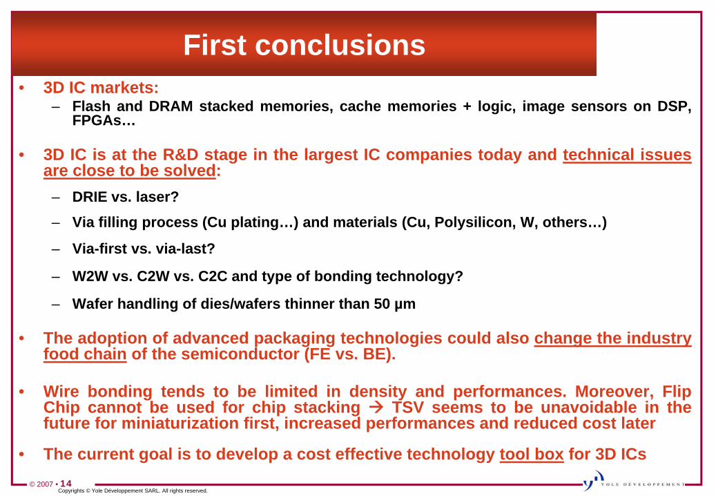
First conclusions• 3D IC markets:
– Flash and DRAM stacked memories, cache memories + logic, image sensors on DSP,FPGAs…
• 3D IC is at the R&D stage in the largest IC companies today and technical issuesare close to be solved:
– DRIE vs. laser?– Via filling process (Cu plating…) and materials (Cu, Polysilicon, W, others…)
– Via-first vs. via-last?
– W2W vs. C2W vs. C2C and type of bonding technology?
– Wafer handling of dies/wafers thinner than 50 µm
• The adoption of advanced packaging technologies could also change the industryfood chain of the semiconductor (FE vs. BE).
• Wire bonding tends to be limited in density and performances. Moreover, FlipChip cannot be used for chip stacking TSV seems to be unavoidable in thefuture for miniaturization first, increased performances and reduced cost later
• The current goal is to develop a cost effective technology tool box for 3D ICs
© 2007 • 15Copyrights © Yole Développement SARL. All rights reserved.
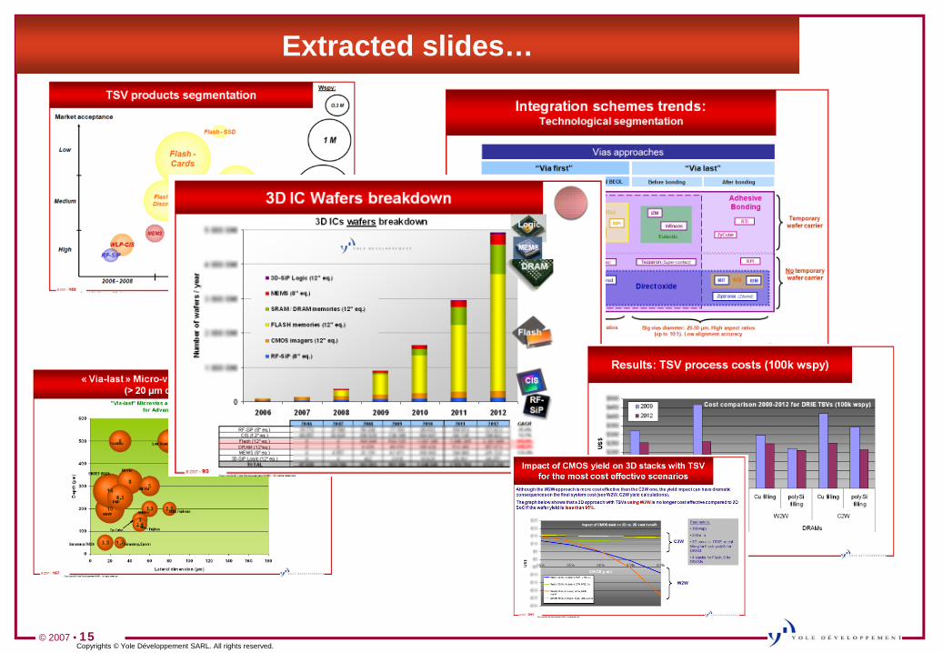
Extracted slides…
© 2007 • 16Copyrights © Yole Développement SARL. All rights reserved.
More information on:www.yole.fr
www.i-micronews.com


![WP91 Lucia Montanaro Kosovo State Building Conundrum 3dic[1]](https://img.pdfslide.net/doc/110x75/577d27671a28ab4e1ea3d6e5/wp91-lucia-montanaro-kosovo-state-building-conundrum-3dic1.jpg)