Embed Size (px)
Citation preview
R&S FS-K72 3G FDD BTS/K74 3GPP HSDPA/UPA BTS Firmware Release 4.10
1154.7023.44 1 E-16
Test and Measurement Division
Release Notes
3G FDD BTS/3GPP HSDPA BTS
Application Firmware R&S FS-K72/FS-K74 Release 4.10 for R&S FSP, FSU, FSQ, FMU Analyzer Firmware 4.1x
Release Note Revision: 2
Printed in the Federal Republic of Germany
R&S FS-K72 3G FDD BTS/K74 3GPP HSDPA/UPA BTS Firmware Release 4.10
1154.7023.44 2 E-16
Contents History ......................................................................................................................... 2 General Topics............................................................................................................ 3
Hardware Requirements ............................................................................................................... 3 Compatibility of R&S FS-K72/K74................................................................................................ 3 Firmware Update of R&S FS-K72/K74 ......................................................................................... 4
Generation of an update disk set for R&S FS-K72/K74 .......................................................... 4 Preparing installation via LAN or USB stick:............................................................................ 5 Performing the Application Firmware Update on the Instrument............................................. 5 Enabling the Application Firmware via License Key Code Entry............................................. 5
Modified Functions..................................................................................................... 6 Problems Eliminated with 4.10 .................................................................................. 8 Modifications to the Operating Manual..................................................................... 8
Modified Chapters for manual operation .................................................................................... 8 Code Domain Power Menu – Overview .................................................................................. 9 Measurement Menu – Overview............................................................................................ 10 Signal Power Check – SPECTRUM EM MASK .................................................................... 11 Root Mean Square Error Vector Magnitude (EVMRMS).......................................................... 13 Error Vector Magnitude (EVMchip) versus chip ...................................................................... 13 Explanation of displayed IQ impairments .............................................................................. 19 Menu MEAS – SPECTRUM EM MASK................................................................................. 21
Modified Chapters for remote operation................................................................................... 22 Advanced channel type estimation (SCPICH)....................................................................... 22 Define channel table using advanced channel types (SCPICH) ........................................... 24 Activating Error Vector Magnitude versus chip measurements............................................. 24 Query result of Error Vector Magnitude versus chip ............................................................. 25 Query result of scrambled chip data for composite constellation display.............................. 25 Query result of Frequency Error vs Slot ................................................................................ 25 Enabling of automatic peak search in spectrum emission mask measurement.................... 26 Query result of peak search list in spectrum emission mask measurement ......................... 26
Appendix: Contact to our hotline ............................................................................ 28
History
Date Rel Note Rev Changes 04 April 2007 1 First revision for R&S FS-K72/R&S FS-K74 version 4.10 22 August 2007 2 Chapter Modifications to the Operating Manual corrected.
The extensions of version 4.00 SP1 were erroneously removed.
R&S FS-K72 3G FDD BTS/K74 3GPP HSDPA/UPA BTS Firmware Release 4.10
1154.7023.44 3 E-16
General Topics Hardware Requirements Please note that R&S FS-K72/K74 requires options R&S FSP-B15 and R&S FSP-B70 in order to run on an R&S FSP. If either of the required hardware options is not installed the unit will not accept the license key for the corresponding firmware application.
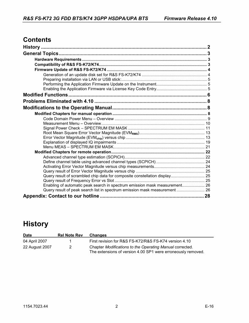
Compatibility of R&S FS-K72/K74 The following table shows the compatible versions of the basic analyzer firmware and the 3G FDD BTS Application Firmware R&S FS-K72 and 3GPP Application Firmware R&S FS-K74 (FS-K74 is supported since version 2.28/3.28):
Table of compatible versions:
R&S FS-K72/K74 Application Firmware
R&S FSP Basic
Firmware
R&S FSU Basic
Firmware
R&S FSQ Basic
Firmware
R&S FSMR Basic
Firmware
R&S FMU Basic
Firmware
4.10 4.10 4.11 4.15 4.16 4.184.01 - - - - 4.084.00 4.00 4.01 4.05 - -3.90 3.90 3.91 3.95 3.96 -3.80 3.80 3.81 3.85 3.86 -3.70 3.70 3.71 3.75 3.76 SP1 -3.60 3.60 3.61 3.65 3.66 SP1 -3.50 3.50 3.51 3.55 - -3.40 3.40 3.41 3.45 - -3.35 - - 3.35 - -3.30 3.30 3.31 - - -3.28 3.20 3.21 3.25 - -3.24 3.10 3.11 3.15 - -3.20 3.00 - 3.05 - -2.60 2.60 2.61 - - -2.40 2.40 2.41 2.45 - -2.35 - - 2.35 - -2.30 2.30 2.31 - - -2.28 2.20 2.21 2.25 - -2.24 2.10 2.11 2.15 - -1.21 - - 2.05 - -1.20 1.80 1.81 1.85 - -1.12 1.70 1.71 1.75 - -1.11 1.60 1.61 1.65 - -1.10 1.50 1.51 - - -1.00 - 1.41 - - -
Application firmware versions 3.xx/4.xx are running on R&S FSPs with order # 1164.4391.xx or R&S FSU with order # 1166.1660.xx or R&S FSQ with operating system XP.
R&S FS-K72 3G FDD BTS/K74 3GPP HSDPA/UPA BTS Firmware Release 4.10
1154.7023.44 4 E-16
Application firmware version 2.xx are running on R&S FSPs with order # 1093.4495.xx or R&S FSU with order # 1129.9003.xx or R&S FSQ with operating system NT.
Firmware Update of R&S FS-K72/K74 The R&S FS-K72/K74 Application Firmware package is available with its own version number. This application firmware package requires an appropriate basic instrument firmware version. Compatible revisions are shown in the table above. Please make sure to have the correct basic firmware version installed prior to installing the R&S FS-K72/K74 Application Firmware. Please refer to the basic firmware version release notes for firmware update information of the basic firmware. Note: R&S FS-K72/74 and R&S FS-K73 are using the same update set. It is therefore required to only
update one of these applications.
Generation of an update disk set for R&S FS-K72/K74 The files needed for the R&S FS-K72/K74 Application Firmware update are available in the FIRMWARE section of the Service Board on GLORIS (R&S FS-K72 and FS-K74 are included in the same disc). If you already have the update disk set you can skip this paragraph. They are grouped according to the disk contents: Disk 1: disk1.bin (self-extracting ZIP file) Disk 2: data3.cab (packed contents of disk 2, will be automatically unpacked by FW update)
The contents of disk 1 are packed in a self-extracting ZIP file and need to be unzipped. For this purpose the following steps are necessary: 1. Create a temporary directory on your local PC (e.g. MyTemp\Extensions\K72 on drive C:) 2. Copy disk1.bin into that directory and rename it to disk1.exe 3. Execute disk1.exe. Under Windows 95/98/NT/2000 this is done best using the following sequence:
<CTRL><ESC> - RUN – C:\MyTemp\Extensions\K72\DISK1 - <ENTER> or <CTRL><ESC> - AUSFÜHREN – C:\MyTemp\Extensions\K72\DISK1 - <ENTER>for a German Windows version. The files will be unzipped.
4. Delete disk1.exe from the temporary directory. data1.cab data1.hdr data2.cab ExecCtrl.exe id.txt ikernel.ex_ ISSetup.exe layout.bin RestInst.exe Setup.exe Setup.ini setup.inx
Please make sure that all filenames exactly match with these printed above before you try to use them for the firmware update. Especially the trailing underscore ('_') as used in ikernel.ex_ or _inst32i.ex_ is essential for correct operation of the update program.
5. Copy the contents of the temporary directory onto update disk #1. The content of the other disk is already packed in the format required by the firmware update program and need no further processing. The files only need to be copied onto disks #2, the number in the filename (minus 1) indicating the corresponding disk number (data3.cab => disk #2).
R&S FS-K72 3G FDD BTS/K74 3GPP HSDPA/UPA BTS Firmware Release 4.10
1154.7023.44 5 E-16
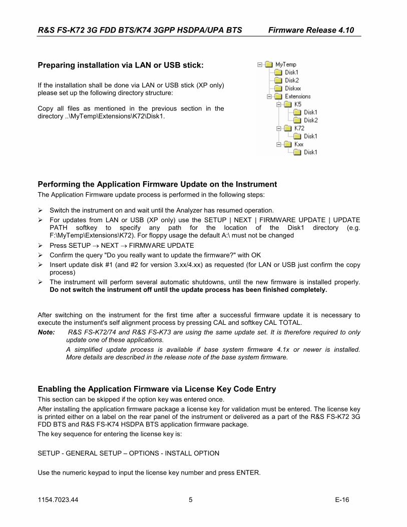
Preparing installation via LAN or USB stick: If the installation shall be done via LAN or USB stick (XP only) please set up the following directory structure: Copy all files as mentioned in the previous section in the directory ..\MyTemp\Extensions\K72\Disk1.
Performing the Application Firmware Update on the Instrument The Application Firmware update process is performed in the following steps: � Switch the instrument on and wait until the Analyzer has resumed operation. � For updates from LAN or USB (XP only) use the SETUP | NEXT | FIRMWARE UPDATE | UPDATE
PATH softkey to specify any path for the location of the Disk1 directory (e.g. F:\MyTemp\Extensions\K72). For floppy usage the default A:\ must not be changed
� Press SETUP → NEXT → FIRMWARE UPDATE � Confirm the query "Do you really want to update the firmware?" with OK � Insert update disk #1 (and #2 for version 3.xx/4.xx) as requested (for LAN or USB just confirm the copy
process) � The instrument will perform several automatic shutdowns, until the new firmware is installed properly.
Do not switch the instrument off until the update process has been finished completely.
After switching on the instrument for the first time after a successful firmware update it is necessary to execute the instument's self alignment process by pressing CAL and softkey CAL TOTAL. Note: R&S FS-K72/74 and R&S FS-K73 are using the same update set. It is therefore required to only
update one of these applications. A simplified update process is available if base system firmware 4.1x or newer is installed. More details are described in the release note of the base system firmware.
Enabling the Application Firmware via License Key Code Entry This section can be skipped if the option key was entered once. After installing the application firmware package a license key for validation must be entered. The license key is printed either on a label on the rear panel of the instrument or delivered as a part of the R&S FS-K72 3G FDD BTS and R&S FS-K74 HSDPA BTS application firmware package. The key sequence for entering the license key is: SETUP - GENERAL SETUP – OPTIONS - INSTALL OPTION Use the numeric keypad to input the license key number and press ENTER.
R&S FS-K72 3G FDD BTS/K74 3GPP HSDPA/UPA BTS Firmware Release 4.10
1154.7023.44 6 E-16
� Each application firmware R&S FS-K72 3G FDD BTS and R&S FS-K74 HSDPA BTS has its own option key. The K72 3G FDD BTS is a prerequisite for installing the K74 HSDPA BTS application firmware!
� Installing FS-K72: option key for FS-K72 must be entered � Installing FS-K74: option key for FS-K72 and option key for FS-K74 must be entered � On a successful validation the message 'option key valid‘ will appear. � If the validation failed, the application firmware is not installed.
The most probable reason will be that the instrument is not equipped with the correct basic firmware version. Therefore a message box will appear asking for installation of the correct basic firmware version. If the application firmware package was not installed prior to entering the license key code, a message will appear asking for installation of the application firmware package. In any case please make sure that the correct basic firmware version and the application firmware package is installed prior to entering the license key code.
Modified Functions The version numbers in brackets indicate the version in which the function was modified. 1. [V1.11] New functions: Antenna Diversity, Sync Type CPICH / SCH 2. [V1.12] Carrier Frequency Error now determined on per slot basis 3. [V1.12] New result display types: Composite Constellation, Power vs. Symbol 4. [V1.12] New: Support for Compressed Mode signals 5. [V1.20] Margin check of xdB margin below Spectrum Emission Mask Limit Lines 6. [V3.20/V1.20] Output of frequency and response value if margin check failed 7. [V3.20/V1.21] Improved sensitivity for code channels with low SN ratio (6dB SNR of a code class 8 channel is sufficient to detect the channel in auto search mode) 8. [V3.20/V1.21] Pilot symbol check added. 9. [V3.20/V1.21] For signalling a detection of a pilot symbol that is different from that of the 3GPP standard the 5th Bit of the status register is used. 10. [V3.24/V2.24] Code Domain Error Power measurement is now available 11. [V3.24/V2.24] Improved Resolution of Trigger to Frame measurement 12. [V3.24/V2.24] Improved absolute accuracy of Trigger to Frame measurement 13. [V3.24/V2.24] Trace statistic available on result summary parameters (MIN Hold, MAX Hold, Averaging) 14. [V3.24/V2.24] Improved compressed mode handling 15. [V3.28/V2.28] Support of FS-K74 HSDPA BTS Test including automatic channel search 16. [V3.28/V2.28] Unit circle display in constellation diagrams 17. [V3.28] Option FS-K9 power sensor support for RF measurement 18. [V3.30/V2.30] New function: Multi-Frame Evaluation 19. [V3.30/V2.30] Detection of SCCPCH is now available 20. [V3.30/V2.30] Improved detection sensitivity for HSDPA channels 21. [V3.30/V2.30] Spectrum emission mask – IEC readout of worst fail position 22. [V3.30/V2.30] Auto channel detection of compressed mode channels 23. [V3.40/V2.40] IEC readout of frame bit-stream
R&S FS-K72 3G FDD BTS/K74 3GPP HSDPA/UPA BTS Firmware Release 4.10
1154.7023.44 7 E-16
24. [V3.40/V2.40] Slot power difference of power versus slot measurement 25. [V3.40/V2.40] Adjacent channel leakage power ratio (ACLR) for multi carrier signals 26. [V3.40/V2.40] Peak list evaluation of spectrum emission mask 27. [V3.40/V2.40] Advanced auto level adjust of multi carrier signals 28. [V3.40/V2.40] Autolevel Adjust for channel power measurement and statistic measurement 29. [V3.50/V2.60] Extended scrambling code range 30. [V3.50/V2. 60] Advanced channel type estimation for compressed mode 31. [V3.50/V2. 60] Display of slot format type A and type B 32. [V3.50/V2. 60] Display of TPC Symbols in the first slot of a compressed gap 33. [V3.50/V2. 60] Constellation re-arrangement for 16 QAM in dependence on constellation parameter B 34. [V3.50/V2. 60] Absolute and relative slot power display and differential slot power display added 35. [V3.50/V2. 60] Extended trigger range 36. [V3.50/V2. 60] RF combination measurement (RF Combi) 37. [V3.60/V2.60] Display of frequency error versus slot, phase discontinuity versus slot, symbol magnitude error and symbol phase error 38. [V3.60/V2.60] Result Summary: added value RHO 39. [V3.60/V2.60] Scrambling code input in hex and also in decimal 40. [V3.60/V2.60] HSDPA mode can be switched OFF / ON 41. [V3.60/V2.60] Measurement of timing offset in predefined channel mode 42. [V3.60/V2.60] Multi carrier ACP measurement with independent inter carrier spacing support 43. [V3.60/V2.60] SEM: Extended range definition for peak list and adjustable transition frequency 44. [V3.60/V2.60] External trigger level adjustable from 0.5 to 3.5 V 45. [V3.60/V2.60] Carrier frequency step size softkey available 46. [V3.70/V2.80] Scrambling code auto search 47. [V3.70/V2.80] Channel table compare mode 48. [V3.70/V2.80] Remote command to read out total power versus slot 49. [V3.70/V2.80] ACLR/MCACLR: number of adjacent channels increased to 12, power mode to max hold the power results 50. [V3.70/V2.80] RF COMBI: noise correction mode 51. [V3.80/V2.80] Support for HSUPA within R&S FS-K74 52. [V3.80/V2.80] Trace view available within code domain analyzer 53. [V3.90] List result of scrambling code search 54. [V4.00] Vector error of Error Vector Magnitude (EVM) versus chip 55. [V4.00] Magnitude error of Error Vector Magnitude (EVM) versus chip 56. [V4.00] Phase error of Error Vector Magnitude (EVM) versus chip 57. [V4.00] Spectrum emission mask: List evaluation in lower screen now supported 58. [V4.00SP1] New remote command TRACe:DATA? ATRACE2 59. [V4.10] New remote command CALC:MARK:FUNC:WCDP:RES? PSYMbol | ACHannels
R&S FS-K72 3G FDD BTS/K74 3GPP HSDPA/UPA BTS Firmware Release 4.10
1154.7023.44 8 E-16
Problems Eliminated with 4.10 The version numbers in brackets indicate the version in which the problem was observed for the first time.
• 1. (K72/K74 V2.80/ V3.80) Code domain error power display corrected.According to 3GPP specification the code domain error (CDE) measurement displays the chip error of the signal spread to the channels spreading factor 256. In previous versions the spreading factor of the CDE measurement has been varied by adjusting the spreading factor of the Peak Code Domain Error Power (PCDEP) measurement. According to 3GPP the spreading factor of CDE is fixed to 256 and only the spreading factor of PCDEP may be varied. The unwanted dependency of CDE spreading factor on PCDEP spreading factor has been eliminated within this version.
• 2. (K72/K74 V4.00) Selectable number of pilot symbols in predefined channel table corrected. The correction only applies to compressed mode channels with increased data rate by 2 in predefined mode if a new channel is added to the channel table. In case of an increased data rate, the number of pilot symbols is doubled compared to standard DPCH channels. In the previous version it was not possible to select the correct number of pilot symbols for the following two channel types: CPR_SF2 and CPR_SF2_TPC.
• 3. (K72/K74 V4.00) Predefined Channel Table 3GB_2 corrected (more than 3 DPCH channels).
Modifications to the Operating Manual The R&S FS-K72/K74 3G FDD BTS analyzer functions are included in a separate manual set. Please refer to the following order numbers:
• 1154.7023.44-03 German and English
Modified Chapters for manual operation
R&S FS-K72 3G FDD BTS/K74 3GPP HSDPA/UPA BTS Firmware Release 4.10
1154.7023.44 9 E-16
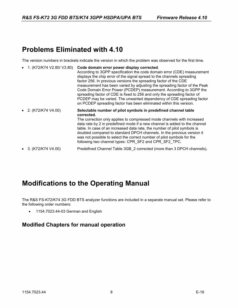
Code Domain Power Menu – OverviewRESULTS SCREEN B
REF LVLADJUST
SELECT
CHANNELSELECT
VS SLOTFREQ ERR
DISCONTPHASE
CAPTURELENGTH
FRAME TOANALYZE
SELECTCHANNEL
SELECTCPICH SLOT
ADJUSTREF LVL
EVMSYMBOL
ERRORSYMB MAG
ERRORSYMB PHASE
CODE DOMERROR
CHANNELTABLE
CONSTSYMBOL
BITSTREAM
CHANNELSELECT
REF LVLADJUST
POWERVS SYMBOL
SELECT
SYMBOLEVM
VS SLOTPOWER
RESULTSUMMARY
CODE DOMPOWER
CHANNELSELECT
REF LVLADJUST
SELECT
EVM (RMS)COMPOSITE
SIGNALCOMPOSITE
DOMAIN ERRPEAK CODE
VS CHIPEVM
CONSTCOMPOSITE
VS CHIPPHASE ERR
VS CHIPMAG ERROR
CHAN CONFEXIT 3GPP
HEADERVALUES
SPECIALADD
LINEINSERT
LINEDELETE
MEAS CHANCONF TABLE
SAVE TABLE
SORT TABLE
PAGE UP
PAGE DOWN
CODE CHANAUTOSEARCH
CODE CHANPREDEFINED
NEW CHANCONF TABL
EDIT CHANCONF TABL
DEL CHANCONF TABL
COPY CHANCONF TABL
TIMING OFSPRED MEAS
CHAN TABLECOMPARE
CAPTURELENGTH
FRAME TOANALYZE
SELECTCHANNEL
SELECTCPICH SLOT
ADJUSTREF LVL
ANT NO.1 2
ANT DIVON OFF
INACT CHANTHRESHOLD
CODE PWRABS REL
SYNC TYPECPICH SCH
POWER REFTOT CPICH
COMP MODEON OFF
POWER DIFFON OFF
SCRAMBLINGCODE
SCRAMBLINGCODE
FORMATHEX DEC
SCRAM CODEAUTO SRCH
SCRAM CODELIST
SIDE BANDNORM INV
NORMALIZEON OFF
INVERT QON OFF
MULTI FRMCAPTURE
MULT CARRON OFF
AUTO SCALEON OFF
CONSTPARAM B
HS-DPA/UPAON OFF
SETTINGS
Figure 1: Code Domain Power Menu – Overview
R&S FS-K72 3G FDD BTS/K74 3GPP HSDPA/UPA BTS Firmware Release 4.10
1154.7023.44 10 E-16
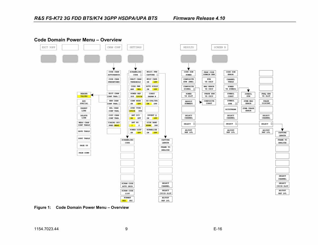
Measurement Menu – Overview
ADJUSTSETTINGS
ADJUSTREF LVL
% POWERBANDWIDTH
ACLR LIMITCHECK
EDIT ACLRLIMIT
CHANNELBANDWIDTH
ADJ CHANBANDWIDTH
ADJ CHANSPACING
ACLRABS REL
CHAN PWR/ HZ
NO. OFADJ CHAN
ADJUSTSETTINGS
SWEEPTIME
NOISE CORRON OFF
FAST ACLRON OFF
DIAGRAMFULL SIZE
ADJUSTREF LVL
ADJUSTREF LVL
NO. OFADJ CHAN
NO. OFTX CHAN
CHANNELSPACING
ACP REFSETTINGS
CP / ACPABS REL
CHAN PWR/ HZ
ADJUSTSETTINGS
ACP LIMITCHECK
EDITACP LIMIT
CHANNELBANDWIDTH
ADJUSTREF LVL
CP / ACPCONFIG
SWEEPTIME
NOISE CORRON OFF
FAST ACPON OFF
DIAGRAMFULL SIZE
X-ACHISREF LEVEL
X-ACHISRANGE
Y-ACHISMAX VALUE
Y-ACHISMIN VALUE
ADJUSTSETTINGS
DEFAULTSETTINGS
MARKERPERCENT
APD
CCDF
NO OFSAMPLES
SCALING
ADJUSTSETTINGS
CONTMEAS
SINGLEMEAS
ADJUSTREF LVL
ADJUSTREF LVL
LIMIT LINEAUTO
LIMIT LINEMANUAL
RESTORESTD LINES
LIMIT LINEUSER
PEAKSEARCH
PEAKSPER RANGE
MARGIN
VIEWPEAK LIST
ADJUSTREF LVL
% POWERBANDWIDTH
CP / ACPCONFIG
SWEEPTIME
See Code DomainPower Menu
NOISE CORRON OFF
POWERMODE DELTA LIM
SORT BY
EXPORTASCII FILE
UPPAGE
FREQUENCYSORT BY
DECIM SEP. ,
DOWNPAGE
ADJUSTREF LVL
LIMIT LINEAUTO
LIMIT LINEMANUAL
RESTORESTD LINES
LIMIT LINEUSER
LISTEVALUATION
PEAKSEARCH
PEAKSPER RANGE
MARGIN
VIEWPEAK LIST
30kHz/1MHzTRANSITION
LINE 1DISPLAY
LIMIT LINESHIFT X
LINE 2DISPLAY
LINE 1FREQUENCY
LINE 2FREQUENCY
LINE 1TIME
LINE 2TIME
NEW LIMITLINE
LIMIT LINESELECT
EDIT LIMITLINE
LIMIT LINECOPY
LIMIT LINEDELETE
X OFFSET
Y OFFSET
DISPLAYLINE
VALUEINSERT
LIMIT LINESHIFT X
NAME
VALUES
VALUEDELETE
LIMIT LINESHIFT Y
LIMIT LINESAVE
ACLR
POWER
SPECTRUMEM MASK
OCCUPIEDBANDWIDTH
CODE DOMPOWER
STATISTICS
MULT CARRACLR
RFCOMBI
MEAS
Figure 2: Overview of menus - measurements
R&S FS-K72 3G FDD BTS/K74 3GPP HSDPA/UPA BTS Firmware Release 4.10
1154.7023.44 11 E-16
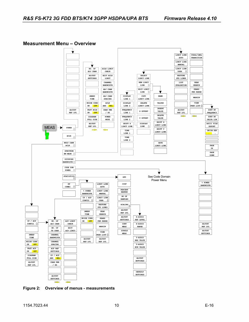
Signal Power Check – SPECTRUM EM MASK MEAS key
LINE 1DISPLAY
LIMIT LINESHIFT X
LINE 2DISPLAY
LINE 1FREQUENCY
LINE 2FREQUENCY
LINE 1TIME
LINE 2TIME
NEW LIMITLINE
LIMIT LINESELECT
EDIT LIMITLINE
LIMIT LINECOPY
LIMIT LINEDELETE
X OFFSET
Y OFFSET
DISPLAYLINE
VALUEINSERT
LIMIT LINESHIFT X
NAME
VALUES
VALUEDELETE
LIMIT LINESHIFT Y
LIMIT LINESAVE
DELTA LIMSORT BY
EXPORTASCII FILE
UPPAGE
FREQUENCYSORT BY
DECIM SEP. ,
DOWNPAGE
PEAKSEARCH
PEAKSPER RANGE
MARGIN
VIEWPEAK LIST
30kHz/1MHzTRANSITION
ADJUSTREF LVL
LIMIT LINEAUTO
LIMIT LINEMANUAL
RESTORESTD LINES
LIMIT LINEUSER
LISTEVALUATION
SPECTRUMEM MASK
Figure 3: Spectrum emission mask measurement menu
R&S FS-K72 3G FDD BTS/K74 3GPP HSDPA/UPA BTS Firmware Release 4.10
1154.7023.44 12 E-16
The SPECTRUM EM MASK softkey starts the determination of the power of the 3GPP FDD signal in defined offsets from the carrier and compares the power values with a spectral mask specified by 3GPP.
IEC/IEEE bus command: :CONF:WCDP:MEAS ESP Query of results: :CALC:LIMit:FAIL? and visual evaluation
R&S FS-K72 3G FDD BTS/K74 3GPP HSDPA/UPA BTS Firmware Release 4.10
1154.7023.44 13 E-16
Root Mean Square Error Vector Magnitude (EVMRMS)
EVM (RMS)COMPOSITE The COMPOSITE EVM (RMS) softkey selects the root mean square
composite EVM (modulation accuracy) display model according to the 3GPP specification. During the composite EVM measurement, the square root of the mean squared errors between the real and imaginary components of the received signal and an ideal reference signal (EVM refererenced to the total signal) is determined. Thus, composite EVM is a measurement of the composite signal.
2560|%1001
0
2
0
2
=⋅−
=
∑
∑−
=
= Nx
xsEVM N
nn
N
nnn
RMS
where: EVMRMS - root mean square of the vector error of the composite signal
sn - complex chip value of received signal xn - complex chip value of reference signal n - index number for mean power calculation of
received and reference signal. N - number of chips at each CPICH slot
IEC/IEEE bus command: :CALC2:FEED "XTIM:CDP:MACC" Query of result: :TRAC2:DATA? TRAC2 UNIT: [%] Range: [0% … 100%]
Error Vector Magnitude (EVMchip) versus chip
DOMAIN ERRPEAK CODE
VS CHIPEVM
CONSTCOMPOSITE
VS CHIPPHASE ERR
VS CHIPMAG ERROR
SIGNALCOMPOSITE The COMPOSITE SIGNAL softkey opens a submenu for evaluation
dispays of the compsite WCDMA signal versus time. Different measurements are supported: PEAK CODE DOMAIN ERR:
Peak Code Domain Error Projection of the error between the received signal and the ideal reference signal onto the spreading factor of code class 8 and subsequent averaging using the symbols of each slot of the difference signal. The maximum value of all codes is displayed versus the CPICH slot number [screen B].
R&S FS-K72 3G FDD BTS/K74 3GPP HSDPA/UPA BTS Firmware Release 4.10
1154.7023.44 14 E-16
EVM VS CHIP: Error Vector Magnitude versus chip Square root of square difference between received signal and reference signal at chip level, displayed for each chip.
MAG ERROR VS CHIP: Magnitude Error versus chip Difference between the amplitude of the received signal and the reference signal at chip level, displayed for each chip.
PHASE ERROR VS CHIP:
Phase Error versus chip Phase difference between the received signal vector and the reference signal vector at chip level, displayed for each chip.
COMPOSITE CONST Composite Constellation diagram Constellation diagram of received signal (scrambled chips) [screen B].
DOMAIN ERRPEAK CODE The PEAK CODE DOMAIN ERR softkey selects the peak code domain
error display mode. In line with the 3GPP specifications, the error between the measurement signal and the ideal reference signal is projected onto the various spreading factors. The result consists of one numerical value per slot for the peak code domain error value. The measurement interval is the slot spacing of the CPICH (timing offset of 0 chips referenced to the beginning of the frame).
IEC/IEEE bus command: :CALC2:FEED "XTIM:CDP:ERR:PCD Query of result: :TRAC2:DATA? TRAC2
VS CHIPEVM The EVM VS CHIP softkey activates the Error Vector Magnitude (EVM)
versus chip display. The EVM is displayed for all chips of the slected slot. . The selected slot can be varied by the SELECT CPICH SLOT softkey. The EVM is calculated by the root of the square difference of received signal and reference signal. The reference signal is estimated from the channel configuration of .all active channels. The EVM is related to the square root of the mean power of reference signal and given in percent.
R&S FS-K72 3G FDD BTS/K74 3GPP HSDPA/UPA BTS Firmware Release 4.10
1154.7023.44 15 E-16
( )[ ]10|2560|%1001 1
0
2
2
−∈=⋅−
=
∑−
=
NkNx
N
xsEVM N
nn
kkk K
where: EVMk - vector error of the chip EVM of chip number k sk - complex chip value of received signal xk - complex chip value of reference signal k - index number of the evaluated chip n - index number for mean power calculation of
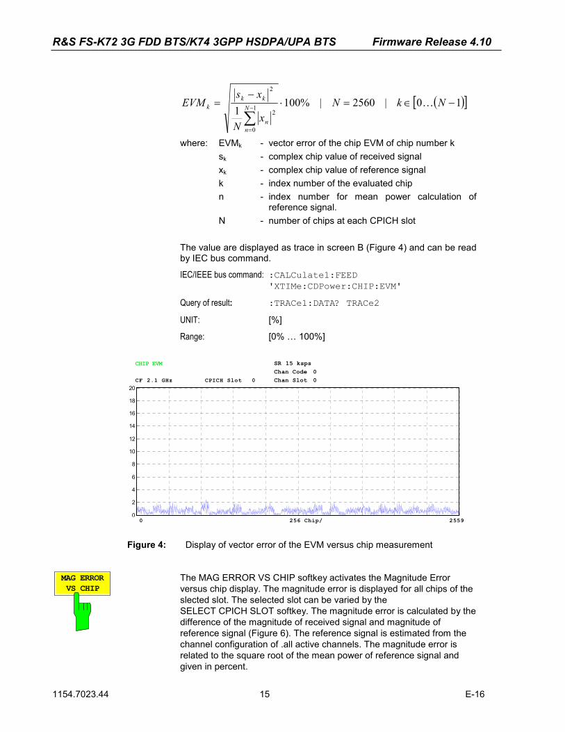
reference signal. N - number of chips at each CPICH slot The value are displayed as trace in screen B (Figure 4) and can be read by IEC bus command.
IEC/IEEE bus command: :CALCulate1:FEED 'XTIMe:CDPower:CHIP:EVM'
Query of result: :TRACe1:DATA? TRACe2 UNIT: [%] Range: [0% … 100%]
256 512 768 1024 1280 1536 1792 2048 2304 25600
2
4
6
8
10
12
14
16
18
20
Chan Code 0Chan Slot 0
SR 15 ksps
CF 2.1 GHz CPICH Slot 0
CHIP EVM
0 256 Chip/ 2559
Figure 4: Display of vector error of the EVM versus chip measurement
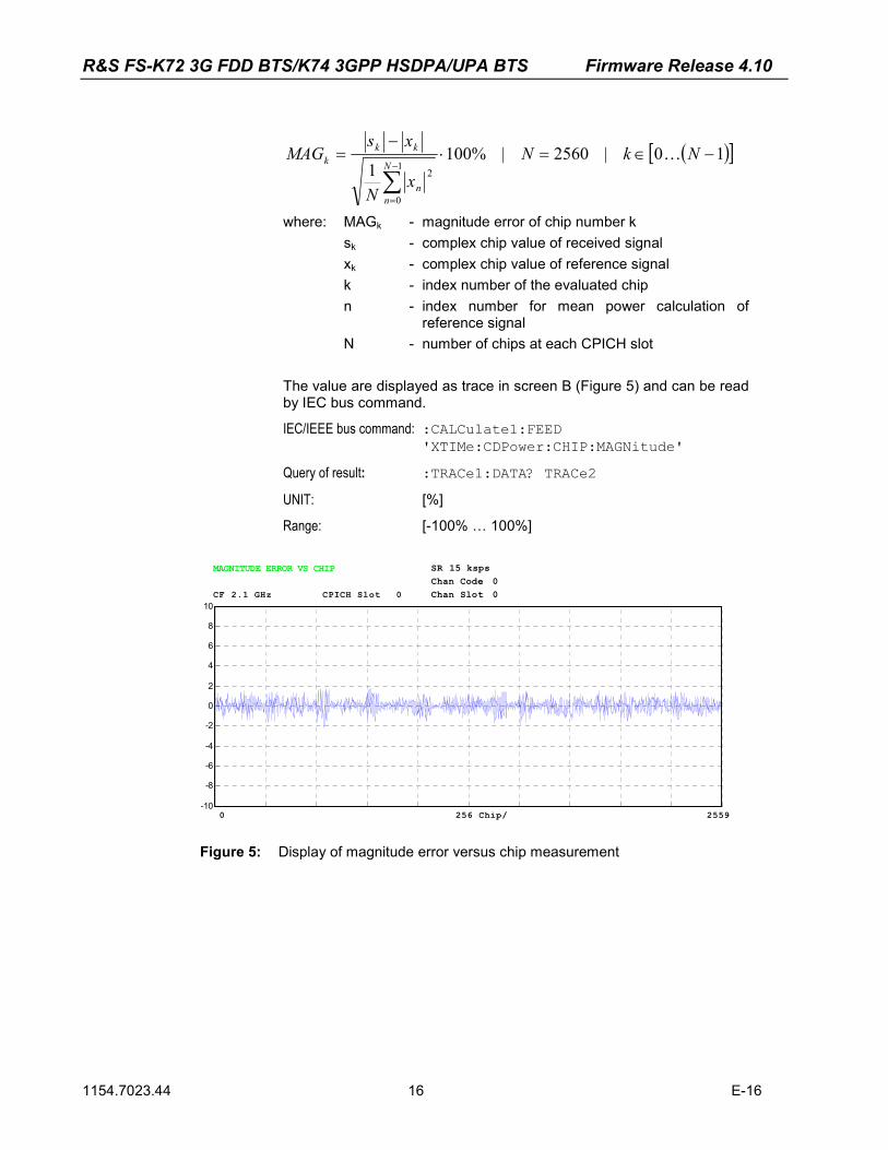
VS CHIPMAG ERROR The MAG ERROR VS CHIP softkey activates the Magnitude Error
versus chip display. The magnitude error is displayed for all chips of the slected slot. The selected slot can be varied by the SELECT CPICH SLOT softkey. The magnitude error is calculated by the difference of the magnitude of received signal and magnitude of reference signal (Figure 6). The reference signal is estimated from the channel configuration of .all active channels. The magnitude error is related to the square root of the mean power of reference signal and given in percent.
R&S FS-K72 3G FDD BTS/K74 3GPP HSDPA/UPA BTS Firmware Release 4.10
1154.7023.44 16 E-16
( )[ ]10|2560|%100
1 1
0
2
−∈=⋅−
=
∑−
=
NkNx
N
xsMAG
N
nn
kkk K
where: MAGk - magnitude error of chip number k sk - complex chip value of received signal xk - complex chip value of reference signal k - index number of the evaluated chip n - index number for mean power calculation of
reference signal N - number of chips at each CPICH slot The value are displayed as trace in screen B (Figure 5) and can be read by IEC bus command.
IEC/IEEE bus command: :CALCulate1:FEED 'XTIMe:CDPower:CHIP:MAGNitude'
Query of result: :TRACe1:DATA? TRACe2 UNIT: [%]
Range: [-100% … 100%]
256 512 768 1024 1280 1536 1792 2048 2304 2560-10
-8
-6
-4
-2
0
2
4
6
8
10
Chan Code 0Chan Slot 0
SR 15 ksps
CF 2.1 GHz CPICH Slot 0
MAGNITUDE ERROR VS CHIP
0 256 Chip/ 2559
Figure 5: Display of magnitude error versus chip measurement
R&S FS-K72 3G FDD BTS/K74 3GPP HSDPA/UPA BTS Firmware Release 4.10
1154.7023.44 17 E-16
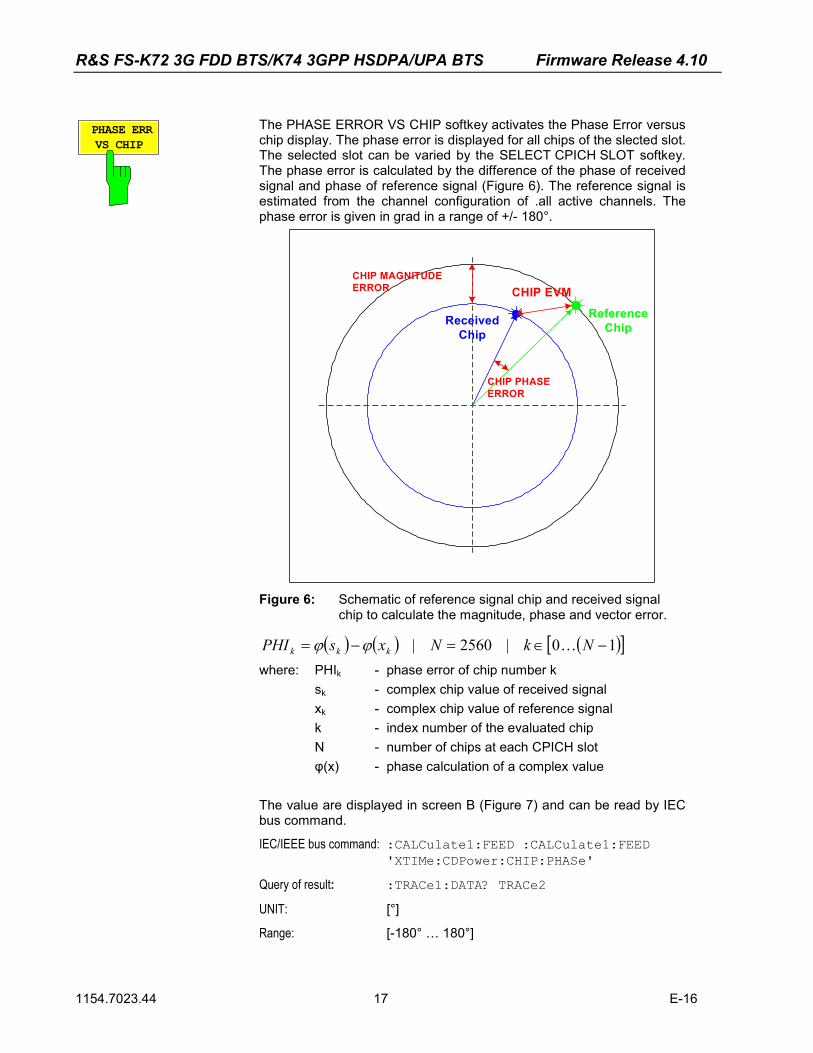
VS CHIPPHASE ERR The PHASE ERROR VS CHIP softkey activates the Phase Error versus
chip display. The phase error is displayed for all chips of the slected slot. The selected slot can be varied by the SELECT CPICH SLOT softkey. The phase error is calculated by the difference of the phase of received signal and phase of reference signal (Figure 6). The reference signal is estimated from the channel configuration of .all active channels. The phase error is given in grad in a range of +/- 180°.
ReceivedChip
ReferenceChip
CHIP EVMCHIP MAGNITUDEERROR
CHIP PHASEERROR
Figure 6: Schematic of reference signal chip and received signal
chip to calculate the magnitude, phase and vector error.
( ) ( ) ( )[ ]10|2560| −∈=−= NkNxsPHI kkk Kϕϕwhere: PHIk - phase error of chip number k sk - complex chip value of received signal xk - complex chip value of reference signal k - index number of the evaluated chip N - number of chips at each CPICH slot φ(x) - phase calculation of a complex value The value are displayed in screen B (Figure 7) and can be read by IEC bus command.
IEC/IEEE bus command: :CALCulate1:FEED :CALCulate1:FEED 'XTIMe:CDPower:CHIP:PHASe'
Query of result: :TRACe1:DATA? TRACe2 UNIT: [°] Range: [-180° … 180°]
R&S FS-K72 3G FDD BTS/K74 3GPP HSDPA/UPA BTS Firmware Release 4.10
1154.7023.44 18 E-16
256 512 768 1024 1280 1536 1792 2048 2304 2560-40
-30
-20
-10
0
10
20
30
40
Chan Code 0Chan Slot 0
SR 15 ksps
CF 2.1 GHz CPICH Slot 0
PHASE ERROR VS CHIP
0 256 Chip/ 2559
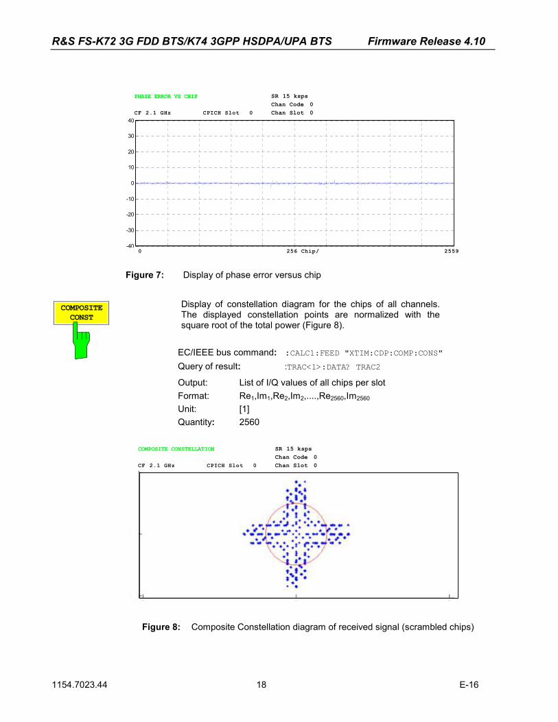
Figure 7: Display of phase error versus chip
CONSTCOMPOSITE Display of constellation diagram for the chips of all channels.
The displayed constellation points are normalized with the square root of the total power (Figure 8).
EC/IEEE bus command: :CALC1:FEED "XTIM:CDP:COMP:CONS" Query of result: :TRAC<1>:DATA? TRAC2
Output: List of I/Q values of all chips per slot Format: Re1,Im1,Re2,Im2,....,Re2560,Im2560 Unit: [1] Quantity: 2560
Chan Code 0Chan Slot 0
SR 15 ksps
CF 2.1 GHz CPICH Slot 0
COMPOSITE CONSTELLATION
Figure 8: Composite Constellation diagram of received signal (scrambled chips)
R&S FS-K72 3G FDD BTS/K74 3GPP HSDPA/UPA BTS Firmware Release 4.10
1154.7023.44 19 E-16
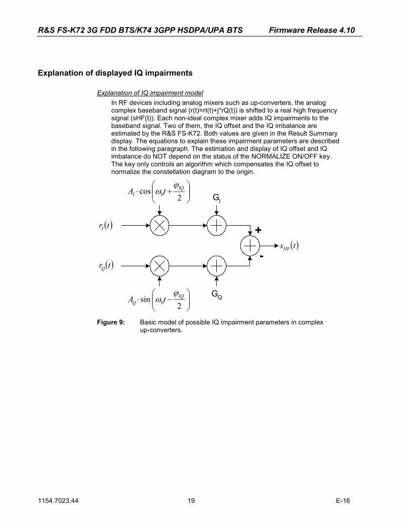
Explanation of displayed IQ impairments
Explanation of IQ impairment modelIn RF devices including analog mixers such as up-converters, the analog complex baseband signal (r(t)=rI(t)+j*rQ(t)) is shifted to a real high frequency signal (sHF(t)). Each non-ideal complex mixer adds IQ impairments to the baseband signal. Two of them, the IQ offset and the IQ imbalance are estimated by the R&S FS-K72. Both values are given in the Result Summary display. The equations to explain these impairment parameters are described in the following paragraph. The estimation and display of IQ offset and IQ imbalance do NOT depend on the status of the NORMALIZE ON/OFF key. The key only controls an algorithm which compensates the IQ offset to normalize the constellation diagram to the origin.
+⋅
2cos 0
IQI tA
ϕω
−⋅
2sin 0
IQQ tA
ϕω
GI
GQ
+
-( )tsHF
( )trQ
( )trI
Figure 9: Basic model of possible IQ impairment parameters in complex up-converters.
R&S FS-K72 3G FDD BTS/K74 3GPP HSDPA/UPA BTS Firmware Release 4.10
1154.7023.44 20 E-16
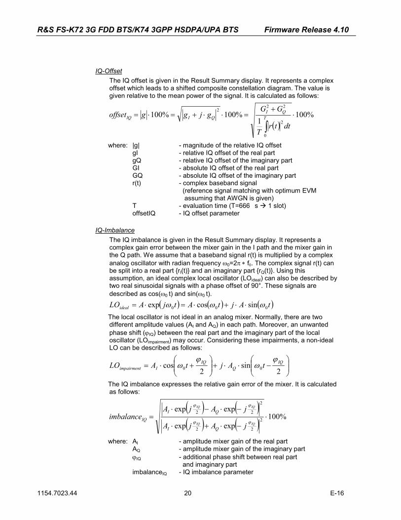
IQ-Offset
The IQ offset is given in the Result Summary display. It represents a complex offset which leads to a shifted composite constellation diagram. The value is given relative to the mean power of the signal. It is calculated as follows:
( )%100
1%100%100
0
2
222
⋅+
=⋅⋅+=⋅=
∫T
QIQIIQ
dttrT
GGgjggoffset
where: |g| - magnitude of the relative IQ offset gI - relative IQ offset of the real part gQ - relative IQ offset of the imaginary part GI - absolute IQ offset of the real part GQ - absolute IQ offset of the imaginary part r(t) - complex baseband signal (reference signal matching with optimum EVM assuming that AWGN is given) T - evaluation time (T=666�s � 1 slot) offsetIQ - IQ offset parameter
IQ-ImbalanceThe IQ imbalance is given in the Result Summary display. It represents a complex gain error between the mixer gain in the I path and the mixer gain in the Q path. We assume that a baseband signal r(t) is multiplied by a complex analog oscillator with radian frequency ω0=2π ∗ f0. The complex signal r(t) can be split into a real part {rI(t)} and an imaginary part {rQ(t)}. Using this assumption, an ideal complex local oscillator (LOideal) can also be described by two real sinusoidal signals with a phase offset of 90°. These signals are described as cos(ω0 t) and sin(ω0 t).
( ) ( ) ( )tAjtAtjALOideal 000 sincosexp ωωω ⋅⋅+⋅=⋅=The local oscillator is not ideal in an analog mixer. Normally, there are two different amplitude values (AI and AQ) in each path. Moreover, an unwanted phase shift (ϕIQ) between the real part and the imaginary part of the local oscillator (LOimpairment) may occur. Considering these impairments, a non-ideal LO can be described as follows:
−⋅⋅+
+⋅=
2sin
2cos 00
IQQ
IQIimpairment tAjtALO
ϕω
ϕω
The IQ imbalance expresses the relative gain error of the mixer. It is calculated as follows:
( ) ( )( ) ( ) %100
expexp
expexp2
22
2
22⋅
−⋅+⋅
−⋅−⋅=
IQIQ
IQIQ
jAjA
jAjAimbalance
QI
QI
IQ ϕϕ
ϕϕ
where: AI - amplitude mixer gain of the real part AQ - amplitude mixer gain of the imaginary part ϕIQ - additional phase shift between real part and imaginary part imbalanceIQ - IQ imbalance parameter
R&S FS-K72 3G FDD BTS/K74 3GPP HSDPA/UPA BTS Firmware Release 4.10
1154.7023.44 21 E-16
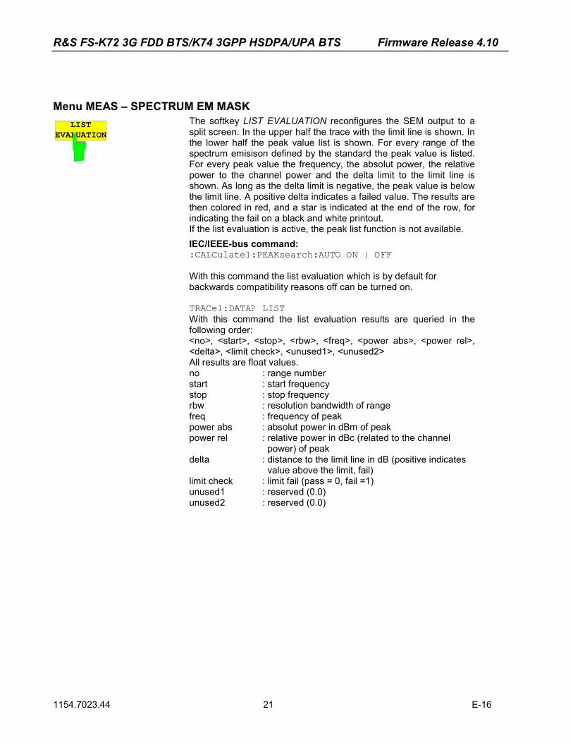
Menu MEAS – SPECTRUM EM MASK LIST
EVALUATIONThe softkey LIST EVALUATION reconfigures the SEM output to a split screen. In the upper half the trace with the limit line is shown. In the lower half the peak value list is shown. For every range of the spectrum emisison defined by the standard the peak value is listed. For every peak value the frequency, the absolut power, the relative power to the channel power and the delta limit to the limit line is shown. As long as the delta limit is negative, the peak value is below the limit line. A positive delta indicates a failed value. The results are then colored in red, and a star is indicated at the end of the row, for indicating the fail on a black and white printout. If the list evaluation is active, the peak list function is not available.
IEC/IEEE-bus command: :CALCulate1:PEAKsearch:AUTO ON | OFF With this command the list evaluation which is by default for backwards compatibility reasons off can be turned on. TRACe1:DATA? LIST With this command the list evaluation results are queried in the following order: <no>, <start>, <stop>, <rbw>, <freq>, <power abs>, <power rel>, <delta>, <limit check>, <unused1>, <unused2> All results are float values. no : range number start : start frequency stop : stop frequency rbw : resolution bandwidth of range freq : frequency of peak power abs : absolut power in dBm of peak power rel : relative power in dBc (related to the channel power) of peak delta : distance to the limit line in dB (positive indicates value above the limit, fail) limit check : limit fail (pass = 0, fail =1) unused1 : reserved (0.0) unused2 : reserved (0.0)
R&S FS-K72 3G FDD BTS/K74 3GPP HSDPA/UPA BTS Firmware Release 4.10
1154.7023.44 22 E-16
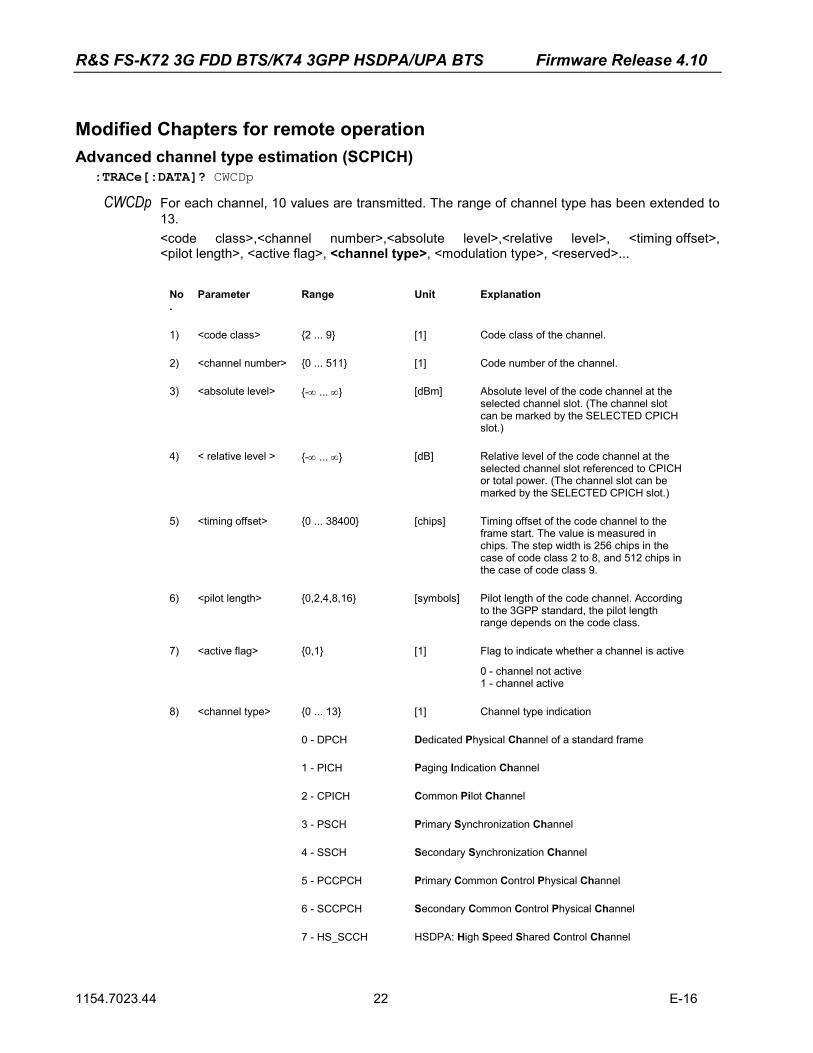
Modified Chapters for remote operation Advanced channel type estimation (SCPICH)
:TRACe[:DATA]? CWCDp CWCDp For each channel, 10 values are transmitted. The range of channel type has been extended to
13. <code class>,<channel number>,<absolute level>,<relative level>, <timing offset>,
<pilot length>, <active flag>, <channel type>, <modulation type>, <reserved>...
No.
Parameter Range Unit Explanation
1) <code class> {2 ... 9} [1] Code class of the channel.
2) <channel number> {0 ... 511} [1] Code number of the channel.
3) <absolute level> {-∞ ... ∞} [dBm] Absolute level of the code channel at the selected channel slot. (The channel slot can be marked by the SELECTED CPICH slot.)
4) < relative level > {-∞ ... ∞} [dB] Relative level of the code channel at the selected channel slot referenced to CPICH or total power. (The channel slot can be marked by the SELECTED CPICH slot.)
5) <timing offset> {0 ... 38400} [chips] Timing offset of the code channel to the frame start. The value is measured in chips. The step width is 256 chips in the case of code class 2 to 8, and 512 chips in the case of code class 9.
6) <pilot length> {0,2,4,8,16} [symbols] Pilot length of the code channel. According to the 3GPP standard, the pilot length range depends on the code class.
7) <active flag> {0,1} [1] Flag to indicate whether a channel is active
0 - channel not active 1 - channel active
8) <channel type> {0 ... 13} [1] Channel type indication
0 - DPCH Dedicated Physical Channel of a standard frame
1 - PICH Paging Indication Channel
2 - CPICH Common Pilot Channel
3 - PSCH Primary Synchronization Channel
4 - SSCH Secondary Synchronization Channel
5 - PCCPCH Primary Common Control Physical Channel
6 - SCCPCH Secondary Common Control Physical Channel
7 - HS_SCCH HSDPA: High Speed Shared Control Channel
R&S FS-K72 3G FDD BTS/K74 3GPP HSDPA/UPA BTS Firmware Release 4.10
1154.7023.44 23 E-16
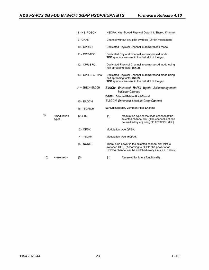
8 - HS_PDSCH HSDPA: High Speed Physical Downlink Shared Channel
9 - CHAN Channel without any pilot symbols (QPSK modulated)
10 - CPRSD Dedicated Physical Channel in compressed mode
11 - CPR-TPC Dedicated Physical Channel in compressed mode TPC symbols are sent in the first slot of the gap.
12 - CPR-SF/2 Dedicated Physical Channel in compressed mode using half spreading factor (SF/2).
13 - CPR-SF/2-TPC Dedicated Physical Channel in compressed mode using half spreading factor (SF/2). TPC symbols are sent in the first slot of the gap.
14 – EHICH-ERGCH E-HICH: Enhanced HARQ Hybrid Acknowledgement Indicator Channel
E-RGCH: Enhanced Relative Grant Channel
15 - EAGCH E-AGCH: Enhanced Absolute Grant Channel
16 – SCPICH SCPICH: Secondary Common Pilot Channel
9) <modulation type>
{2,4,15} [1] Modulation type of the code channel at the selected channel slot. (The channel slot can be marked by adjusting SELECT CPICH slot.)
2 - QPSK Modulation type QPSK.
4 - 16QAM Modulation type 16QAM.
15 - NONE There is no power in the selected channel slot [slot is switched OFF]. (According to 3GPP, the power of an HSDPA channel can be switched every 2 ms, i.e. 3 slots.)
10) <reserved> {0} [1] Reserved for future functionality.
R&S FS-K72 3G FDD BTS/K74 3GPP HSDPA/UPA BTS Firmware Release 4.10
1154.7023.44 24 E-16
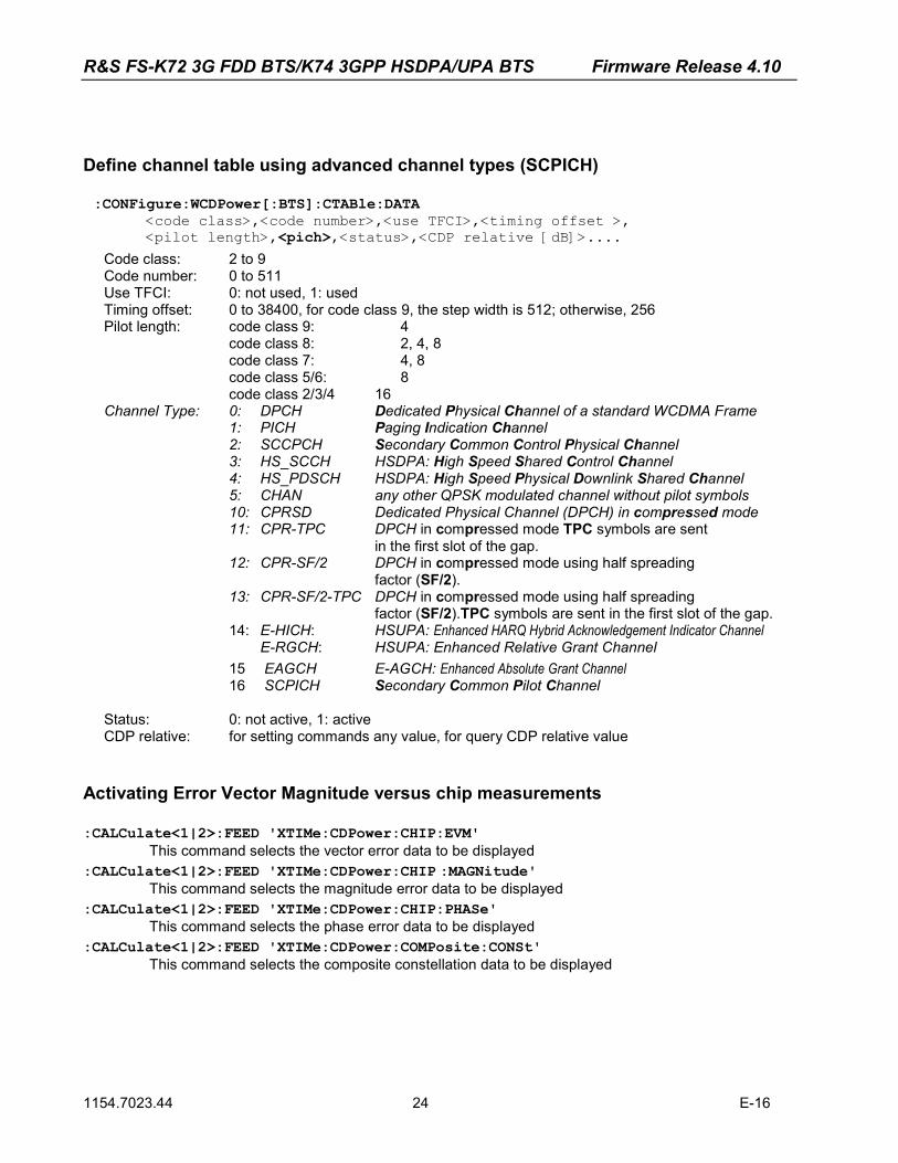
Define channel table using advanced channel types (SCPICH) :CONFigure:WCDPower[:BTS]:CTABle:DATA
<code class>,<code number>,<use TFCI>,<timing offset >, <pilot length>,<pich>,<status>,<CDP relative [dB]>....
Code class: 2 to 9 Code number: 0 to 511 Use TFCI: 0: not used, 1: used Timing offset: 0 to 38400, for code class 9, the step width is 512; otherwise, 256 Pilot length: code class 9: 4 code class 8: 2, 4, 8 code class 7: 4, 8 code class 5/6: 8 code class 2/3/4 16 Channel Type: 0: DPCH Dedicated Physical Channel of a standard WCDMA Frame 1: PICH Paging Indication Channel 2: SCCPCH Secondary Common Control Physical Channel 3: HS_SCCH HSDPA: High Speed Shared Control Channel 4: HS_PDSCH HSDPA: High Speed Physical Downlink Shared Channel 5: CHAN any other QPSK modulated channel without pilot symbols 10: CPRSD Dedicated Physical Channel (DPCH) in compressed mode 11: CPR-TPC DPCH in compressed mode TPC symbols are sent in the first slot of the gap.
12: CPR-SF/2 DPCH in compressed mode using half spreading factor (SF/2). 13: CPR-SF/2-TPC DPCH in compressed mode using half spreading factor (SF/2).TPC symbols are sent in the first slot of the gap. 14: E-HICH: HSUPA: Enhanced HARQ Hybrid Acknowledgement Indicator Channel
E-RGCH: HSUPA: Enhanced Relative Grant Channel 15 EAGCH E-AGCH: Enhanced Absolute Grant Channel 16 SCPICH Secondary Common Pilot Channel
Status: 0: not active, 1: active CDP relative: for setting commands any value, for query CDP relative value
Activating Error Vector Magnitude versus chip measurements :CALCulate<1|2>:FEED 'XTIMe:CDPower:CHIP:EVM'
This command selects the vector error data to be displayed :CALCulate<1|2>:FEED 'XTIMe:CDPower:CHIP :MAGNitude'
This command selects the magnitude error data to be displayed :CALCulate<1|2>:FEED 'XTIMe:CDPower:CHIP:PHASe'
This command selects the phase error data to be displayed :CALCulate<1|2>:FEED 'XTIMe:CDPower:COMPosite:CONSt'
This command selects the composite constellation data to be displayed
R&S FS-K72 3G FDD BTS/K74 3GPP HSDPA/UPA BTS Firmware Release 4.10
1154.7023.44 25 E-16
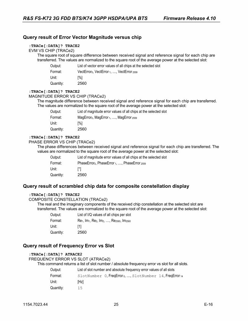
Query result of Error Vector Magnitude versus chip :TRACe[:DATA]? TRACE2 EVM VS CHIP (TRACe2)
The square root of square difference between received signal and reference signal for each chip are transferred. The values are normalized to the square root of the average power at the selected slot:
Output: List of vector error values of all chips at the selected slot Format: VectError0, VectError 1, ...., VectError 2559 Unit: [%] Quantity: 2560
:TRACe[:DATA]? TRACE2 MAGNITUDE ERROR VS CHIP (TRACe2)
The magnitude difference between received signal and reference signal for each chip are transferred. The values are normalized to the square root of the average power at the selected slot:
Output: List of magnitude error values of all chips at the selected slot Format: MagError0, MagError 1, ...., MagError 2559 Unit: [%] Quantity: 2560
:TRACe[:DATA]? TRACE2 PHASE ERROR VS CHIP (TRACe2)
The phase differences between received signal and reference signal for each chip are transferred. The values are normalized to the square root of the average power at the selected slot:
Output: List of magnitude error values of all chips at the selected slot Format: PhaseError0, PhaseError 1, ...., PhaseError 2559 Unit: [°] Quantity: 2560
Query result of scrambled chip data for composite constellation display :TRACe[:DATA]? TRACE2 COMPOSITE CONSTELLATION (TRACe2)
The real and the imaginary components of the received chip constellation at the selected slot are transferred. The values are normalized to the square root of the average power at the selected slot:
Output: List of I/Q values of all chips per slot Format: Re1, Im1, Re2, Im2, ...., Re2560, Im2560 Unit: [1] Quantity: 2560
Query result of Frequency Error vs Slot :TRACe[:DATA]? ATRACE2 FREQUENCY ERROR VS SLOT (ATRACe2)
This command returns a list of slot number / absolute frequency error vs slot for all slots. Output: List of slot number and absolute frequency error values of all slots Format: SlotNumber 0, FreqError 0, ...., SlotNumber 14, FreqError 14 Unit: [Hz] Quantity: 15
R&S FS-K72 3G FDD BTS/K74 3GPP HSDPA/UPA BTS Firmware Release 4.10
1154.7023.44 26 E-16
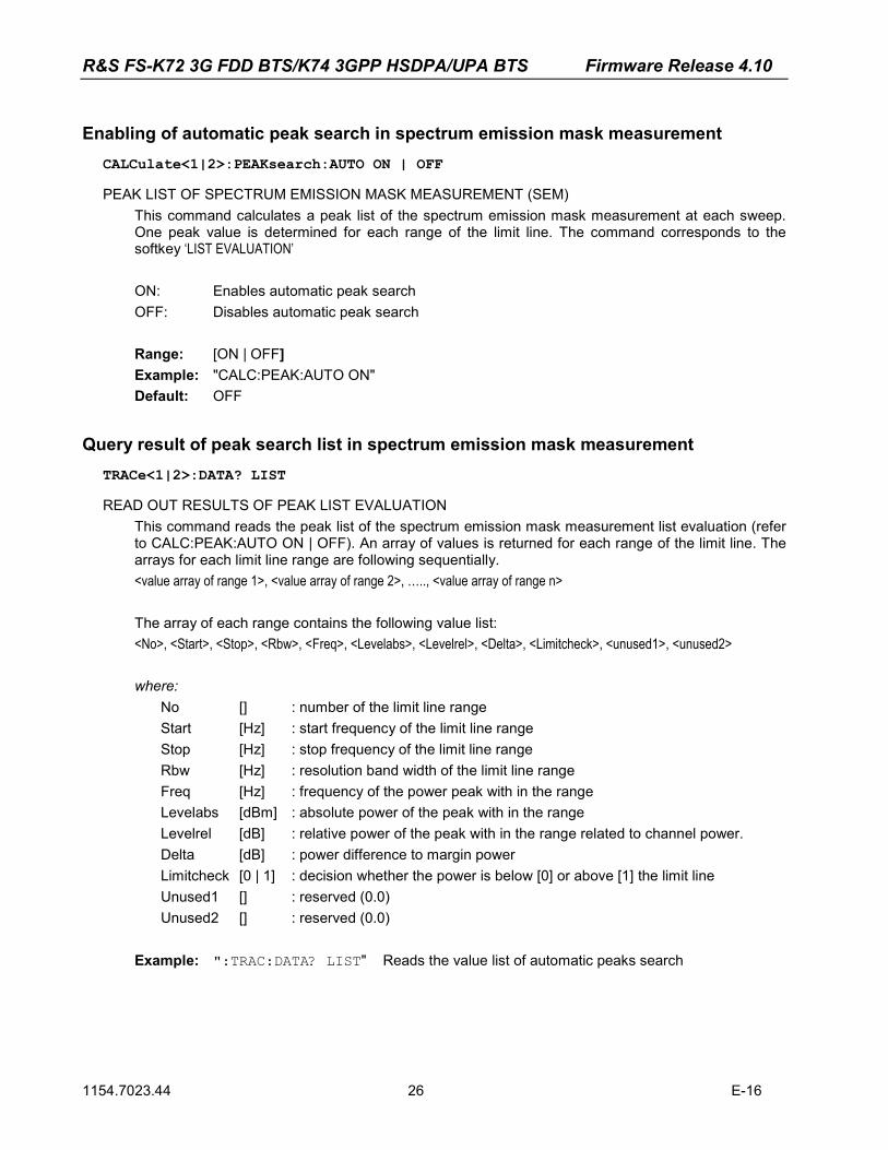
Enabling of automatic peak search in spectrum emission mask measurement CALCulate<1|2>:PEAKsearch:AUTO ON | OFF
PEAK LIST OF SPECTRUM EMISSION MASK MEASUREMENT (SEM) This command calculates a peak list of the spectrum emission mask measurement at each sweep. One peak value is determined for each range of the limit line. The command corresponds to the softkey ‘LIST EVALUATION’
ON: Enables automatic peak search OFF: Disables automatic peak search Range: [ON | OFF]Example: "CALC:PEAK:AUTO ON" Default: OFF
Query result of peak search list in spectrum emission mask measurement TRACe<1|2>:DATA? LIST
READ OUT RESULTS OF PEAK LIST EVALUATION This command reads the peak list of the spectrum emission mask measurement list evaluation (refer to CALC:PEAK:AUTO ON | OFF). An array of values is returned for each range of the limit line. The arrays for each limit line range are following sequentially. <value array of range 1>, <value array of range 2>, ….., <value array of range n> The array of each range contains the following value list: <No>, <Start>, <Stop>, <Rbw>, <Freq>, <Levelabs>, <Levelrel>, <Delta>, <Limitcheck>, <unused1>, <unused2> where:
No [] : number of the limit line range Start [Hz] : start frequency of the limit line range Stop [Hz] : stop frequency of the limit line range Rbw [Hz] : resolution band width of the limit line range Freq [Hz] : frequency of the power peak with in the range Levelabs [dBm] : absolute power of the peak with in the range Levelrel [dB] : relative power of the peak with in the range related to channel power. Delta [dB] : power difference to margin power Limitcheck [0 | 1] : decision whether the power is below [0] or above [1] the limit line Unused1 [] : reserved (0.0) Unused2 [] : reserved (0.0)
Example: ":TRAC:DATA? LIST" Reads the value list of automatic peaks search
R&S FS-K72 3G FDD BTS/K74 3GPP HSDPA/UPA BTS Firmware Release 4.10
1154.7023.44 27 E-16
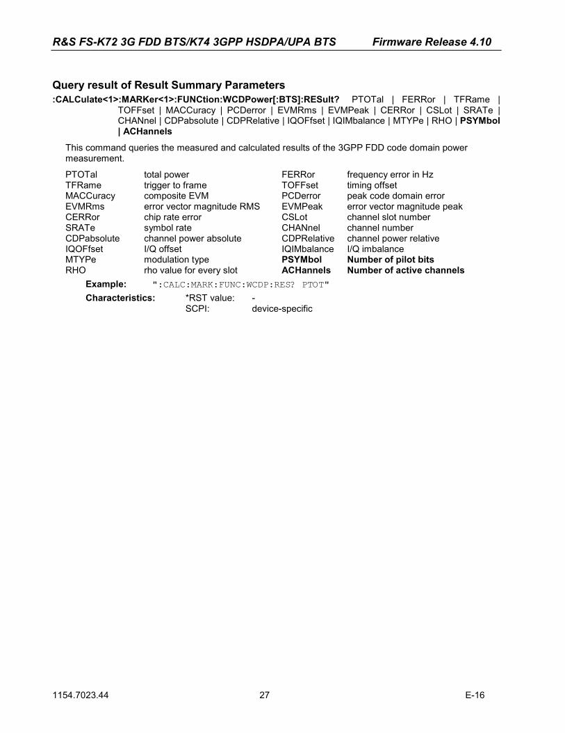
Query result of Result Summary Parameters :CALCulate<1>:MARKer<1>:FUNCtion:WCDPower[:BTS]:RESult? PTOTal | FERRor | TFRame |
TOFFset | MACCuracy | PCDerror | EVMRms | EVMPeak | CERRor | CSLot | SRATe | CHANnel | CDPabsolute | CDPRelative | IQOFfset | IQIMbalance | MTYPe | RHO | PSYMbol | ACHannels
This command queries the measured and calculated results of the 3GPP FDD code domain power measurement.
PTOTal total power FERRor frequency error in Hz TFRame trigger to frame TOFFset timing offset MACCuracy composite EVM PCDerror peak code domain error EVMRms error vector magnitude RMS EVMPeak error vector magnitude peak CERRor chip rate error CSLot channel slot number SRATe symbol rate CHANnel channel number CDPabsolute channel power absolute CDPRelative channel power relative IQOFfset I/Q offset IQIMbalance I/Q imbalance MTYPe modulation type PSYMbol Number of pilot bits RHO rho value for every slot ACHannels Number of active channels
Example: ":CALC:MARK:FUNC:WCDP:RES? PTOT" Characteristics: *RST value: - SCPI: device-specific
R&S FS-K72 3G FDD BTS/K74 3GPP HSDPA/UPA BTS Firmware Release 4.10
1154.7023.44 28 E-16
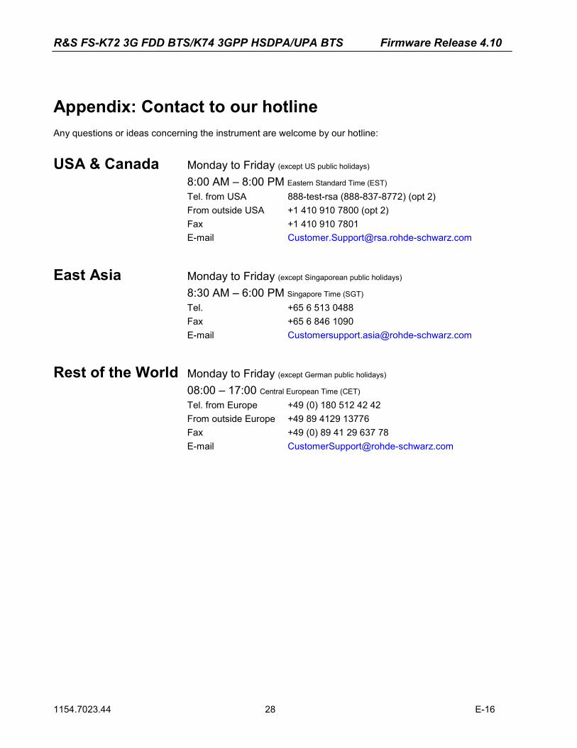
Appendix: Contact to our hotline Any questions or ideas concerning the instrument are welcome by our hotline:
USA & Canada Monday to Friday (except US public holidays)
8:00 AM – 8:00 PM Eastern Standard Time (EST)
Tel. from USA 888-test-rsa (888-837-8772) (opt 2) From outside USA +1 410 910 7800 (opt 2) Fax +1 410 910 7801 E-mail [email protected]
East Asia Monday to Friday (except Singaporean public holidays)
8:30 AM – 6:00 PM Singapore Time (SGT)
Tel. +65 6 513 0488 Fax +65 6 846 1090 E-mail [email protected]
Rest of the World Monday to Friday (except German public holidays)
08:00 – 17:00 Central European Time (CET)
Tel. from Europe +49 (0) 180 512 42 42 From outside Europe +49 89 4129 13776 Fax +49 (0) 89 41 29 637 78 E-mail [email protected]


![M-bts Photo Checklist (3g) Outdoor - Suryani Sudirman [ Email ]](https://img.pdfslide.net/doc/110x75/5695d2681a28ab9b029a4cdd/m-bts-photo-checklist-3g-outdoor-suryani-sudirman-email-.jpg)