Embed Size (px)
Citation preview
W25Q256JV
Publication Release Date: August 03, 2017
Revision G
3V 256M-BIT
SERIAL FLASH MEMORY WITH
DUAL/QUAD SPI
W25Q256JV
- 1 -
Table of Contents
1. GENERAL DESCRIPTIONS ............................................................................................................. 5
2. FEATURES ....................................................................................................................................... 5
3. PACKAGE TYPES AND PIN CONFIGURATIONS ........................................................................... 6
3.1 Pad Configuration WSON 8x6-mm ...................................................................................... 6
3.2 Pad Description WSON 8x6-mm .......................................................................................... 6
3.3 Pin Configuration SOIC 300-mil ........................................................................................... 7
3.4 Pin Description SOIC 300-mil ............................................................................................... 7
3.5 Ball Configuration TFBGA 8x6-mm (5x5 or 6x4 Ball Array) ................................................. 8
3.6 Ball Description TFBGA 8x6-mm ......................................................................................... 8
4. PIN DESCRIPTIONS ........................................................................................................................ 9
4.1 Chip Select (/CS) .................................................................................................................. 9
4.2 Serial Data Input, Output and IOs (DI, DO and IO0, IO1, IO2, IO3) ..................................... 9
4.3 Write Protect (/WP) .............................................................................................................. 9
4.4 HOLD (/HOLD) ..................................................................................................................... 9
4.5 Serial Clock (CLK) ................................................................................................................ 9
4.6 Reset (/RESET)(1) ................................................................................................................. 9
5. BLOCK DIAGRAM .......................................................................................................................... 10
6. FUNCTIONAL DESCRIPTIONS ..................................................................................................... 11
6.1 SPI Operations ................................................................................................................... 11
6.1.1 Standard SPI Instructions ..................................................................................................... 11
6.1.2 Dual SPI Instructions ............................................................................................................ 11
6.1.3 Quad SPI Instructions ........................................................................................................... 11
6.1.4 3-Byte / 4-Byte Address Modes ............................................................................................ 11
6.1.5 Software Reset & Hardware /RESET pin .............................................................................. 12
6.2 Write Protection .................................................................................................................. 13
7. STATUS AND CONFIGURATION REGISTERS ............................................................................ 14
7.1 Status Registers ................................................................................................................. 14
7.1.1 Erase/Write In Progress (BUSY) – Status Only ................................................................ 14
7.1.2 Write Enable Latch (WEL) – Status Only .......................................................................... 14
7.1.3 Block Protect Bits (BP3, BP2, BP1, BP0) – Volatile/Non-Volatile Writable ....................... 15
7.1.4 Top/Bottom Block Protect (TB) – Volatile/Non-Volatile Writable ....................................... 15
7.1.5 Complement Protect (CMP) – Volatile/Non-Volatile Writable ............................................ 15
7.1.1 Status Register Protect (SRP, SRL) – Volatile/Non-Volatile Writable ............................... 16
7.1.2 Erase/Program Suspend Status (SUS) – Status Only....................................................... 17
7.1.3 Security Register Lock Bits (LB3, LB2, LB1) – Volatile/Non-Volatile OTP Writable .......... 17
7.1.4 Quad Enable (QE) – Volatile/Non-Volatile Writable .......................................................... 17
W25Q256JV
Publication Release Date: August 03, 2017
- 2 - Revision G
7.1.5 Current Address Mode (ADS) – Status Only ..................................................................... 18
7.1.6 Power-Up Address Mode (ADP) – Non-Volatile Writable .................................................. 18
7.1.7 Write Protect Selection (WPS) – Volatile/Non-Volatile Writable ....................................... 18
7.1.8 Output Driver Strength (DRV1, DRV0) – Volatile/Non-Volatile Writable ........................... 19
7.1.9 Reserved Bits – Non Functional ........................................................................................ 19
7.1.10 W25Q256JV Status Register Memory Protection (WPS = 0, CMP = 0) ............................. 20
7.1.11 W25Q256JV Status Register Memory Protection (WPS = 0, CMP = 1) ............................. 21
7.1.12 W25Q256JV Individual Block Memory Protection (WPS=1) .............................................. 22
7.2 Extended Address Register – Volatile Writable Only ...................................................... 23
8. INSTRUCTIONS ............................................................................................................................. 24
8.1 Device ID and Instruction Set Tables ................................................................................. 24
8.1.1 Manufacturer and Device Identification ................................................................................ 24
8.1.2 Instruction Set Table 1 (Standard/Dual/Quad SPI, 3-Byte Address Mode)(1) ....................... 25
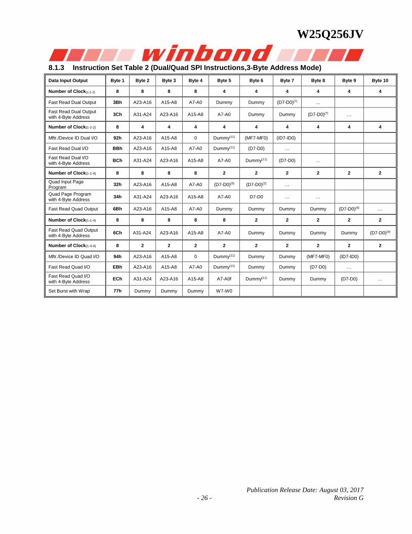
8.1.3 Instruction Set Table 2 (Dual/Quad SPI Instructions,3-Byte Address Mode) ....................... 26
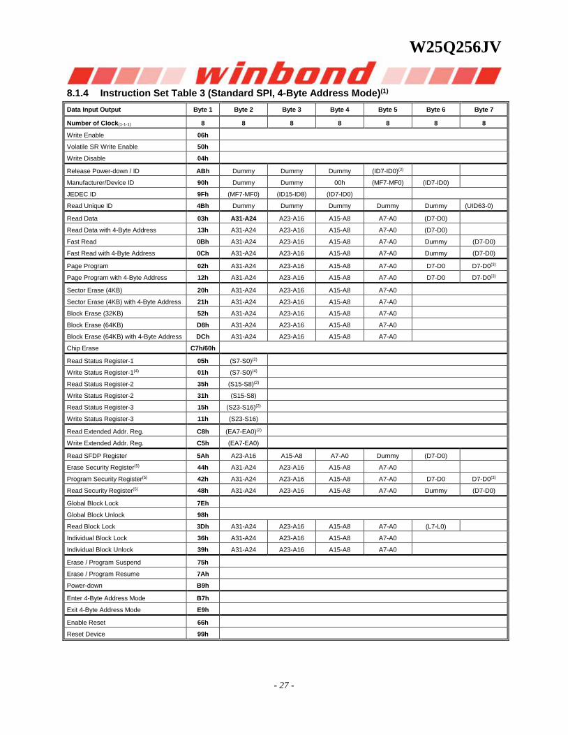
8.1.4 Instruction Set Table 3 (Standard SPI, 4-Byte Address Mode)(1).......................................... 27
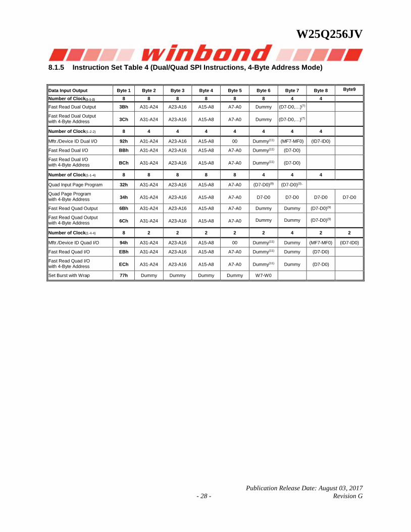
8.1.5 Instruction Set Table 4 (Dual/Quad SPI Instructions, 4-Byte Address Mode) ...................... 28
8.2 Instruction Descriptions ...................................................................................................... 30
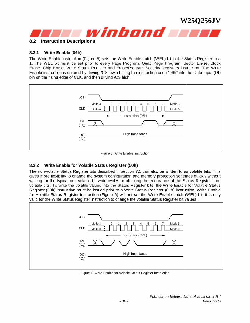
8.2.1 Write Enable (06h) ............................................................................................................... 30
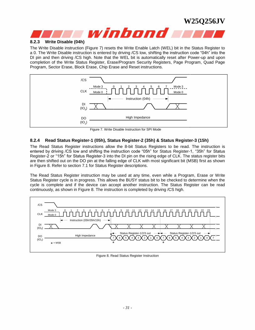
8.2.2 Write Enable for Volatile Status Register (50h) .................................................................... 30
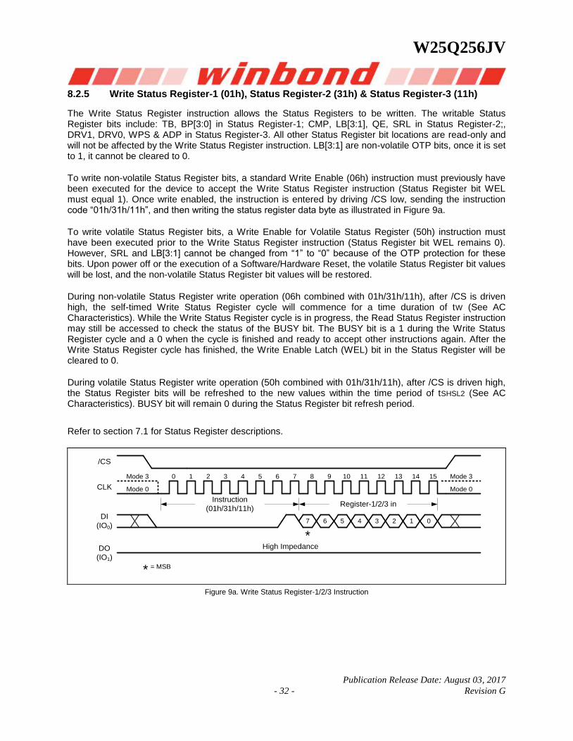
8.2.3 Write Disable (04h) ............................................................................................................... 31
Figure 7. Write Disable Instruction for SPI Mode .............................................................................. 31
8.2.4 Read Status Register-1 (05h), Status Register-2 (35h) & Status Register-3 (15h) .............. 31
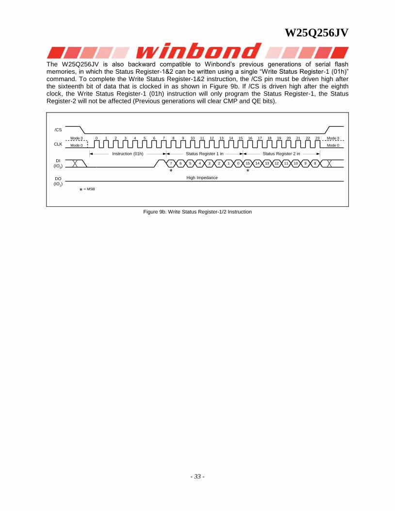
8.2.5 Write Status Register-1 (01h), Status Register-2 (31h) & Status Register-3 (11h) .............. 32
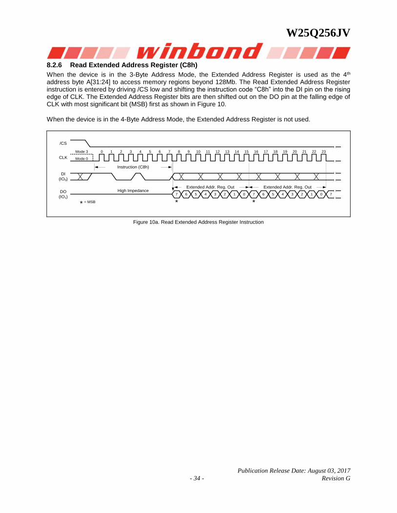
8.2.6 Read Extended Address Register (C8h) .............................................................................. 34
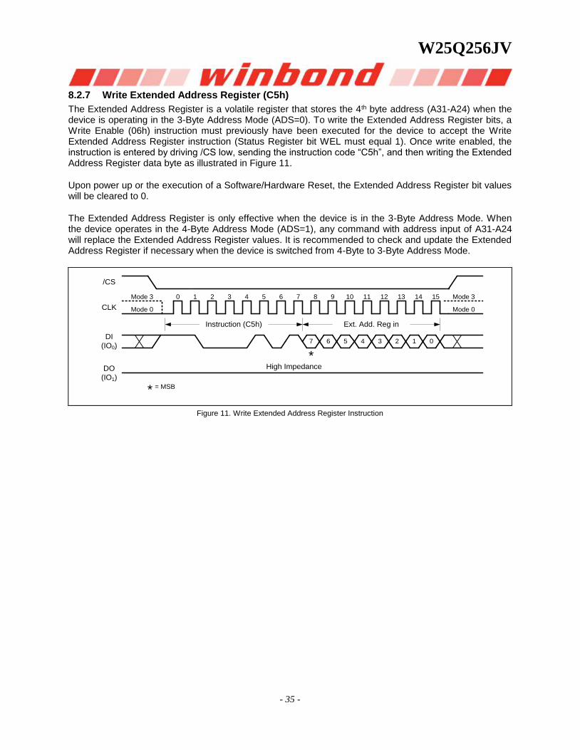
8.2.7 Write Extended Address Register (C5h) .............................................................................. 35
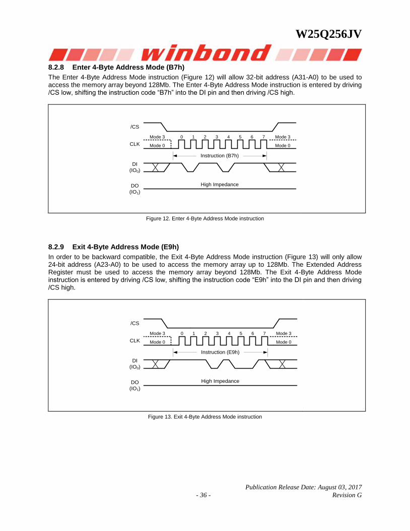
8.2.8 Enter 4-Byte Address Mode (B7h) ........................................................................................ 36
8.2.9 Exit 4-Byte Address Mode (E9h) .......................................................................................... 36
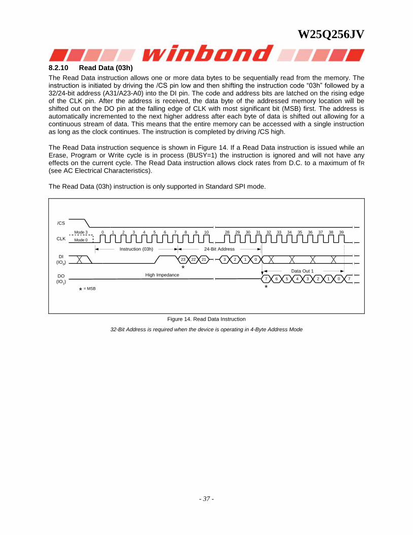
8.2.10 Read Data (03h) ................................................................................................................. 37
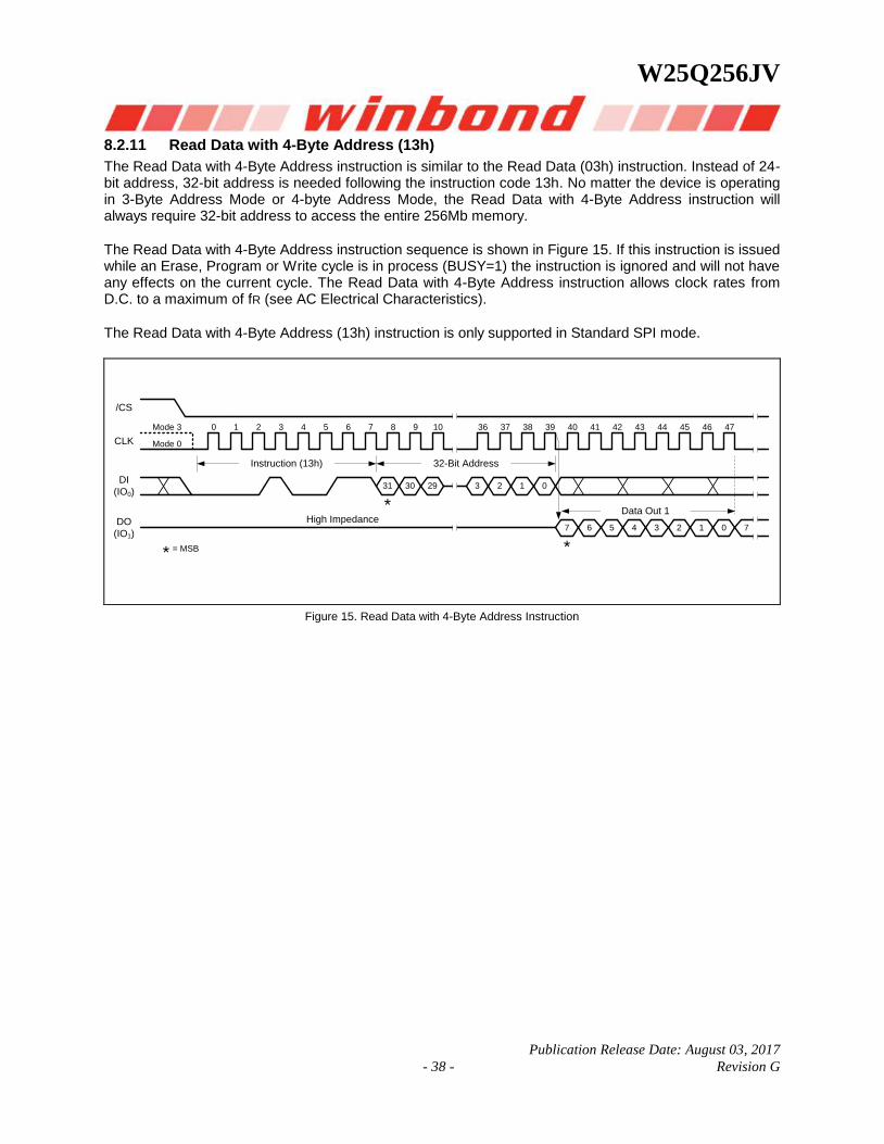
8.2.11 Read Data with 4-Byte Address (13h) ................................................................................ 38
8.2.12 Fast Read (0Bh) ................................................................................................................. 39
8.2.13 Fast Read with 4-Byte Address (0Ch) ................................................................................ 40
8.2.14 Fast Read Dual Output (3Bh) ............................................................................................. 41
8.2.15 Fast Read Dual Output with 4-Byte Address (3Ch) ............................................................ 42
8.2.16 Fast Read Quad Output (6Bh) ............................................................................................ 43
8.2.17 Fast Read Quad Output with 4-Byte Address (6Ch) ........................................................... 44
8.2.18 Fast Read Dual I/O (BBh) ................................................................................................... 45
8.2.19 Fast Read Dual I/O with 4-Byte Address (BCh) .................................................................. 46
8.2.20 Fast Read Quad I/O (EBh) ................................................................................................. 47
8.2.21 Fast Read Quad I/O with 4-Byte Address (ECh) ................................................................ 48
8.2.22 Set Burst with Wrap (77h) .................................................................................................. 49
8.2.23 Page Program (02h) ........................................................................................................... 50
8.2.24 Page Program with 4-Byte Address (12h) .......................................................................... 51
W25Q256JV
- 3 -
8.2.25 Quad Input Page Program (32h) ........................................................................................ 52
8.2.26 Quad Input Page Program with 4-Byte Address (34h) ....................................................... 53
8.2.27 Sector Erase (20h) ............................................................................................................. 54
8.2.28 Sector Erase with 4-Byte Address (21h) ............................................................................. 55
8.2.29 32KB Block Erase (52h) ..................................................................................................... 56
8.2.30 64KB Block Erase (D8h) ..................................................................................................... 57
8.2.31 64KB Block Erase with 4-Byte Address (DCh) ................................................................... 58
8.2.32 Chip Erase (C7h / 60h) ....................................................................................................... 59
8.2.33 Erase / Program Suspend (75h) ......................................................................................... 60
8.2.34 Erase / Program Resume (7Ah) ......................................................................................... 61
8.2.35 Power-down (B9h) .............................................................................................................. 62
8.2.36 Release Power-down / Device ID (ABh) ............................................................................. 63
8.2.37 Read Manufacturer / Device ID (90h) ................................................................................. 64
8.2.38 Read Manufacturer / Device ID Dual I/O (92h) ................................................................... 65
8.2.39 Read Manufacturer / Device ID Quad I/O (94h) ................................................................. 66
8.2.40 Read Unique ID Number (4Bh)........................................................................................... 67
8.2.41 Read JEDEC ID (9Fh) ........................................................................................................ 68
8.2.42 Read SFDP Register (5Ah) ................................................................................................ 69
8.2.43 Erase Security Registers (44h) ........................................................................................... 70
8.2.44 Program Security Registers (42h) ...................................................................................... 71
8.2.45 Read Security Registers (48h) ........................................................................................... 72
8.2.46 Individual Block/Sector Lock (36h) ..................................................................................... 73
8.2.47 Individual Block/Sector Unlock (39h) .................................................................................. 74
8.2.48 Read Block/Sector Lock (3Dh) ........................................................................................... 75
8.2.49 Global Block/Sector Lock (7Eh) .......................................................................................... 76
8.2.50 Global Block/Sector Unlock (98h) ....................................................................................... 76
8.2.51 Enable Reset (66h) and Reset Device (99h) ...................................................................... 77
9. ELECTRICAL CHARACTERISTICS ............................................................................................... 78
9.1 Absolute Maximum Ratings (1) .......................................................................................... 78
9.2 Operating Ranges............................................................................................................... 78
9.3 Power-up Power-down Timing and Requirements ............................................................. 79
9.4 DC Electrical Characteristics .............................................................................................. 80
9.5 AC Measurement Conditions .............................................................................................. 81
9.6 AC Electrical Characteristics(6) ........................................................................................... 82
9.7 AC Electrical Characteristics (cont’d) .............................................................................. 83
9.8 Serial Output Timing ........................................................................................................... 84
9.9 Serial Input Timing .............................................................................................................. 84
9.1 /WP Timing ......................................................................................................................... 84
9.2 PACKAGE SPECIFICATIONs ............................................................................................ 85
9.3 8-Pad WSON 8x6-mm (Package Code E) ......................................................................... 85
9.4 16-Pin SOIC 300-mil (Package Code F) ............................................................................ 86
W25Q256JV
Publication Release Date: August 03, 2017
- 4 - Revision G
9.5 24-Ball TFBGA 8x6-mm (Package Code B, 5x5-1 Ball Array) ........................................... 87
9.6 24-Ball TFBGA 8x6-mm (Package Code C, 6x4 Ball Array) .............................................. 88
9.7 Ordering Information ........................................................................................................... 89
9.8 Valid Part Numbers and Top Side Marking ........................................................................ 90
10. REVISION HISTORY ...................................................................................................................... 91
W25Q256JV
- 5 -
1. GENERAL DESCRIPTIONS
The W25Q256JV (256M-bit) Serial Flash memory provides a storage solution for systems with limited space, pins and power. The 25Q series offers flexibility and performance well beyond ordinary Serial Flash devices. They are ideal for code shadowing to RAM, executing code directly from Dual/Quad SPI (XIP) and storing voice, text and data. The device operates on a single 2.7V to 3.6V power supply with current consumption as low as 1µA for power-down. All devices are offered in space-saving packages.
The W25Q256JV array is organized into 131,072 programmable pages of 256-bytes each. Up to 256 bytes can be programmed at a time. Pages can be erased in groups of 16 (4KB sector erase), groups of 128 (32KB block erase), groups of 256 (64KB block erase) or the entire chip (chip erase). The W25Q256JV has 8,192 erasable sectors and 512 erasable blocks respectively. The small 4KB sectors allow for greater flexibility in applications that require data and parameter storage.
The W25Q256JV supports the standard Serial Peripheral Interface (SPI), Dual/Quad I/O SPI: Serial Clock, Chip Select, Serial Data I/O0 (DI), I/O1 (DO), I/O2, and I/O3. SPI clock frequencies of W25Q256JV of up to 133MHz are supported allowing equivalent clock rates of 266MHz (133MHz x 2) for Dual I/O and 532MHz (133MHz x 4) for Quad I/O when using the Fast Read Dual/Quad I/O. These transfer rates can outperform standard Asynchronous 8 and 16-bit Parallel Flash memories.
Additionally, the device supports JEDEC standard manufacturer and device ID and SFDP Register, a 64-bit Unique Serial Number and three 256-bytes Security Registers.
2. FEATURES
New Family of SpiFlash Memories – W25Q256JV: 256M-bit / 32M-byte – Standard SPI: CLK, /CS, DI, DO – Dual SPI: CLK, /CS, IO0, IO1, – Quad SPI: CLK, /CS, IO0, IO1, IO2, IO3
– 3 or 4-Byte Addressing Mode – Software & Hardware Reset(1)
Highest Performance Serial Flash – 133MHz Standard/Dual/Quad SPI clocks – 266/532MHz equivalent Dual/Quad SPI – 66MB/S continuous data transfer rate
– Min. 100K Program-Erase cycles per sector – More than 20-year data retention
Efficient “Continuous Read” – Quad Peripheral Interface – Allows true XIP (execute in place) operation – Outperforms X16 Parallel Flash
Low Power, Wide Temperature Range – Single 2.7 to 3.6V supply –<1µA Power-down (typ.) – -40°C to +85°C operating range
Flexible Architecture with 4KB sectors – Uniform Sector/Block Erase (4K/32K/64K-Byte) – Program 1 to 256 byte per programmable page – Erase/Program Suspend & Resume
Advanced Security Features – Software and Hardware Write-Protect – Power Supply Lock-Down – Special OTP protection – Top/Bottom, Complement array protection – Individual Block/Sector array protection – 64-Bit Unique ID for each device – Discoverable Parameters (SFDP) Register – 3X256-Bytes Security Registers with OTP locks – Volatile & Non-volatile Status Register Bits
Space Efficient Packaging(2) – 8-pad WSON 8x6-mm – 16-pin SOIC 300-mil (additional /Reset pin) – 24-ball TFBGA 8x6-mm(additional /Reset pin) – Contact Winbond for KGD and other options
Note: 1. Hardware /RESET pin is only available on TFBGA or SOIC16 packages
2. Please contact Winbond for other packages.
W25Q256JV
Publication Release Date: August 03, 2017
- 6 - Revision G
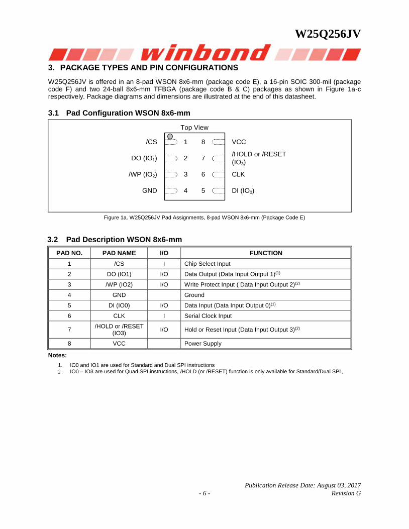
3. PACKAGE TYPES AND PIN CONFIGURATIONS
W25Q256JV is offered in an 8-pad WSON 8x6-mm (package code E), a 16-pin SOIC 300-mil (package code F) and two 24-ball 8x6-mm TFBGA (package code B & C) packages as shown in Figure 1a-c respectively. Package diagrams and dimensions are illustrated at the end of this datasheet.
3.1 Pad Configuration WSON 8x6-mm
1
2
3
4
/CS
DO (IO1)
/WP (IO2)
GND
VCC
/HOLD or /RESET
(IO3)
DI (IO0)
CLK
Top View
8
7
6
5
Figure 1a. W25Q256JV Pad Assignments, 8-pad WSON 8x6-mm (Package Code E)
3.2 Pad Description WSON 8x6-mm
PAD NO. PAD NAME I/O FUNCTION
1 /CS I Chip Select Input
2 DO (IO1) I/O Data Output (Data Input Output 1)(1)
3 /WP (IO2) I/O Write Protect Input ( Data Input Output 2)(2)
4 GND Ground
5 DI (IO0) I/O Data Input (Data Input Output 0)(1)
6 CLK I Serial Clock Input
7 /HOLD or /RESET
(IO3) I/O Hold or Reset Input (Data Input Output 3)(2)
8 VCC Power Supply
Notes:
1. IO0 and IO1 are used for Standard and Dual SPI instructions
2. IO0 – IO3 are used for Quad SPI instructions, /HOLD (or /RESET) function is only available for Standard/Dual SPI.
W25Q256JV
- 7 -
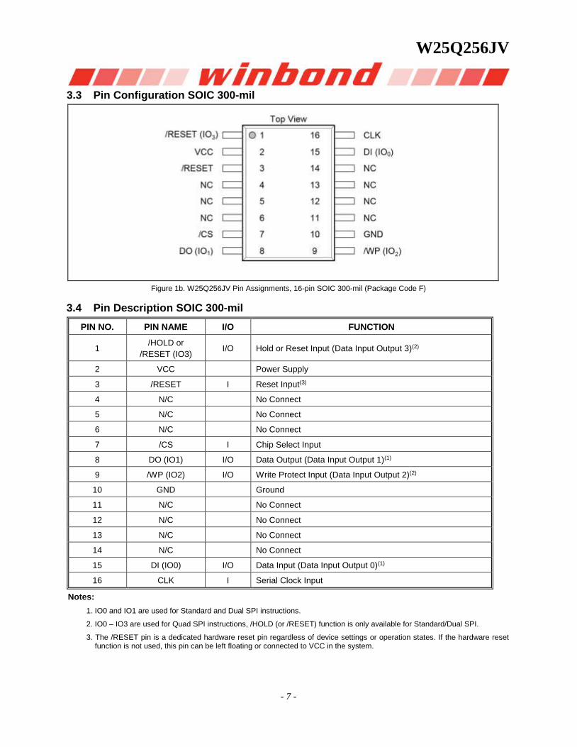
3.3 Pin Configuration SOIC 300-mil
Figure 1b. W25Q256JV Pin Assignments, 16-pin SOIC 300-mil (Package Code F)
3.4 Pin Description SOIC 300-mil
PIN NO. PIN NAME I/O FUNCTION
1 /HOLD or
/RESET (IO3) I/O Hold or Reset Input (Data Input Output 3)(2)
2 VCC Power Supply
3 /RESET I Reset Input(3)
4 N/C No Connect
5 N/C No Connect
6 N/C No Connect
7 /CS I Chip Select Input
8 DO (IO1) I/O Data Output (Data Input Output 1)(1)
9 /WP (IO2) I/O Write Protect Input (Data Input Output 2)(2)
10 GND Ground
11 N/C No Connect
12 N/C No Connect
13 N/C No Connect
14 N/C No Connect
15 DI (IO0) I/O Data Input (Data Input Output 0)(1)
16 CLK I Serial Clock Input
Notes:
1. IO0 and IO1 are used for Standard and Dual SPI instructions.
2. IO0 – IO3 are used for Quad SPI instructions, /HOLD (or /RESET) function is only available for Standard/Dual SPI.
3. The /RESET pin is a dedicated hardware reset pin regardless of device settings or operation states. If the hardware reset function is not used, this pin can be left floating or connected to VCC in the system.
W25Q256JV
Publication Release Date: August 03, 2017
- 8 - Revision G
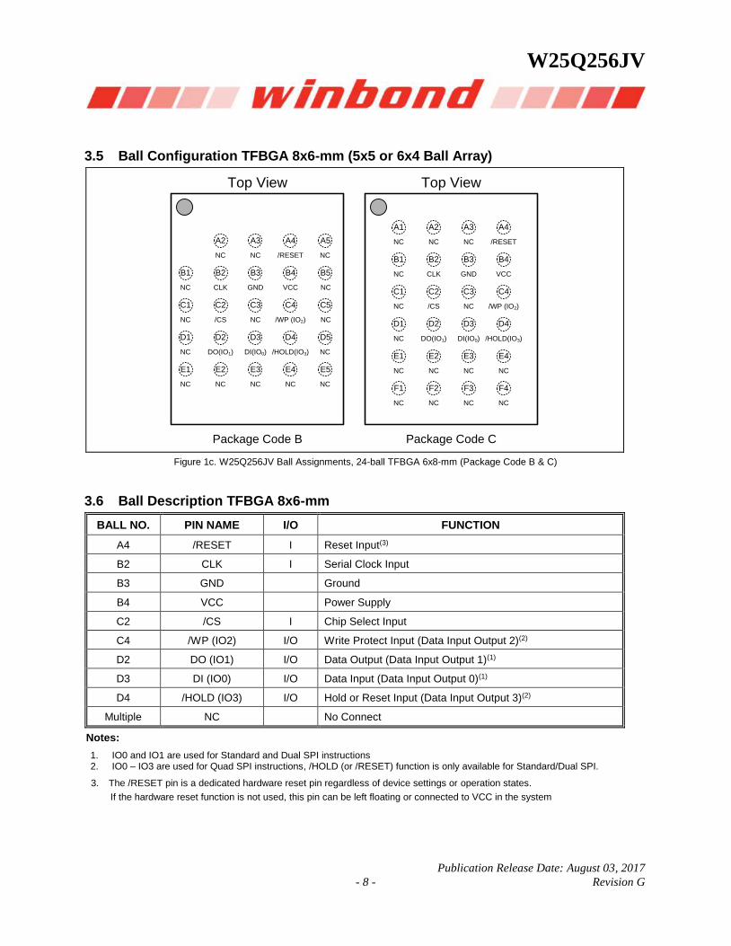
3.5 Ball Configuration TFBGA 8x6-mm (5x5 or 6x4 Ball Array)
D1
/HOLD(IO3)DI(IO0)DO(IO1)
/WP (IO2)
D2 D3 D4
NC
E1
NCNCNC
E2 E3 E4
NC
F1
NCNCNC
F2 F3 F4
NC
A1
/RESETNCNC
A2 A3 A4
NC
B1
VCCGNDCLK
B2 B3 B4
NC
C1
NC/CS
C2 C3 C4
NC
Top View
Package Code C
Top View
D1
/HOLD(IO3)DI(IO0)DO(IO1)
/WP (IO2)
D2 D3 D4
NC
E1
NCNCNC
E2 E3 E4
NC
/RESETNCNC
A2 A3 A4
B1
VCCGNDCLK
B2 B3 B4
NC
C1
NC/CS
C2 C3 C4
NC
D5
E5
A5
B5
C5
NC
NC
NC
NC
NC
Package Code B
Figure 1c. W25Q256JV Ball Assignments, 24-ball TFBGA 6x8-mm (Package Code B & C)
3.6 Ball Description TFBGA 8x6-mm
BALL NO. PIN NAME I/O FUNCTION
A4 /RESET I Reset Input(3)
B2 CLK I Serial Clock Input
B3 GND Ground
B4 VCC Power Supply
C2 /CS I Chip Select Input
C4 /WP (IO2) I/O Write Protect Input (Data Input Output 2)(2)
D2 DO (IO1) I/O Data Output (Data Input Output 1)(1)
D3 DI (IO0) I/O Data Input (Data Input Output 0)(1)
D4 /HOLD (IO3) I/O Hold or Reset Input (Data Input Output 3)(2)
Multiple NC No Connect
Notes:
1. IO0 and IO1 are used for Standard and Dual SPI instructions 2. IO0 – IO3 are used for Quad SPI instructions, /HOLD (or /RESET) function is only available for Standard/Dual SPI.
3. The /RESET pin is a dedicated hardware reset pin regardless of device settings or operation states.
If the hardware reset function is not used, this pin can be left floating or connected to VCC in the system
W25Q256JV
- 9 -
4. PIN DESCRIPTIONS
4.1 Chip Select (/CS)
The SPI Chip Select (/CS) pin enables and disables device operation. When /CS is high the device is deselected and the Serial Data Output (DO, or IO0, IO1, IO2, IO3) pins are at high impedance. When deselected, the devices power consumption will be at standby levels unless an internal erase, program or write status register cycle is in progress. When /CS is brought low the device will be selected, power consumption will increase to active levels and instructions can be written to and data read from the device. After power-up, /CS must transition from high to low before a new instruction will be accepted. The /CS input must track the VCC supply level at power-up and power-down (see “Write Protection” and Figure 58). If needed a pull-up resistor on the /CS pin can be used to accomplish this.
4.2 Serial Data Input, Output and IOs (DI, DO and IO0, IO1, IO2, IO3)
The W25Q256JV supports standard SPI, Dual SPI and Quad SPI operation. Standard SPI instructions use the unidirectional DI (input) pin to serially write instructions, addresses or data to the device on the rising edge of the Serial Clock (CLK) input pin. Standard SPI also uses the unidirectional DO (output) to read data or status from the device on the falling edge of CLK.
Dual and Quad SPI instructions use the bidirectional IO pins to serially write instructions, addresses or data to the device on the rising edge of CLK and read data or status from the device on the falling edge of CLK. Quad SPI instructions require the non-volatile Quad Enable bit (QE) in Status Register-2 to be set. When QE=1, the /WP pin becomes IO2 and the /HOLD pin becomes IO3.
4.3 Write Protect (/WP)
The Write Protect (/WP) pin can be used to prevent the Status Register from being written. Used in conjunction with the Status Register’s Block Protect (CMP, SEC, TB, BP2, BP1 and BP0) bits and Status Register Protect (SRP) bits, a portion as small as a 4KB sector or the entire memory array can be hardware protected. The /WP pin is active low.
4.4 HOLD (/HOLD)
The /HOLD pin allows the device to be paused while it is actively selected. When /HOLD is brought low, while /CS is low, the DO pin will be at high impedance and signals on the DI and CLK pins will be ignored (don’t care). When /HOLD is brought high, device operation can resume. The /HOLD function can be useful when multiple devices are sharing the same SPI signals. The /HOLD pin is active low. When the QE bit of Status Register-2 is set for Quad I/O, the /HOLD pin function is not available since this pin is used for IO3. See Figure 1a-c for the pin configuration of Quad I/O operation.
4.5 Serial Clock (CLK)
The SPI Serial Clock Input (CLK) pin provides the timing for serial input and output operations. ("See SPI Operations")
4.6 Reset (/RESET)(1)
A dedicated hardware /RESET pin is available on SOIC-16 and TFBGA packages. When it’s driven low for a minimum period of ~1µS, this device will terminate any external or internal operations and return to its power-on state.
Note: Hardware /RESET pin is available on SOIC-16 or TFBGA; please contact Winbond for this package.
W25Q256JV
Publication Release Date: August 03, 2017
- 10 - Revision G
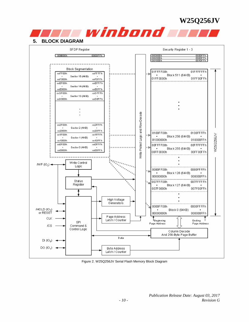
5. BLOCK DIAGRAM
Figure 2. W25Q256JV Serial Flash Memory Block Diagram
W25Q256JV
- 11 -
6. FUNCTIONAL DESCRIPTIONS
6.1 SPI Operations
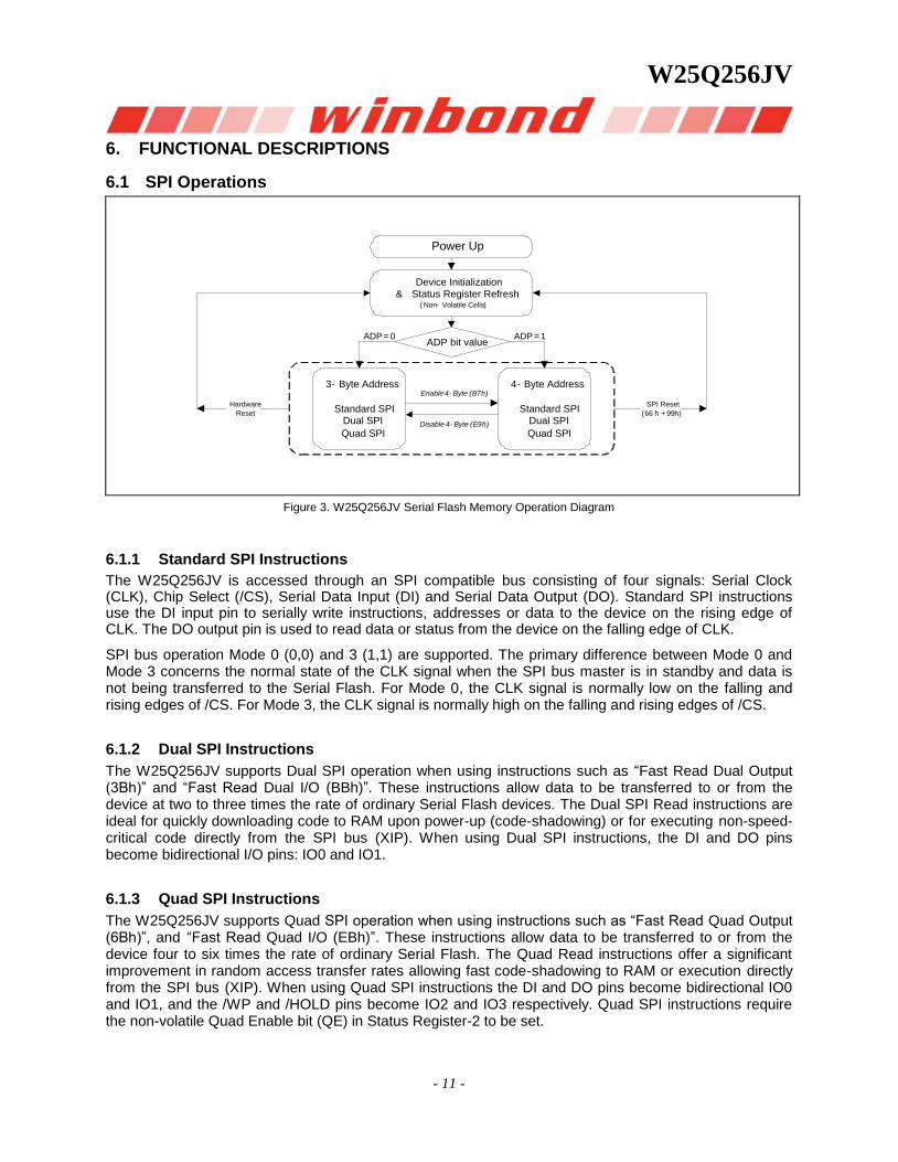
Power Up
ADP bit value
3- Byte Address
Standard SPI
Dual SPI
Quad SPI
Enable 4- Byte (B7h)4- Byte Address
Standard SPI
Dual SPI
Quad SPIDisable 4- Byte (E9h)
SPI Reset
(66 h + 99h)
ADP = 0 ADP = 1
Device Initialization
& Status Register Refresh( Non- Volatile Cells)
Hardware
Reset
Figure 3. W25Q256JV Serial Flash Memory Operation Diagram
6.1.1 Standard SPI Instructions
The W25Q256JV is accessed through an SPI compatible bus consisting of four signals: Serial Clock (CLK), Chip Select (/CS), Serial Data Input (DI) and Serial Data Output (DO). Standard SPI instructions use the DI input pin to serially write instructions, addresses or data to the device on the rising edge of CLK. The DO output pin is used to read data or status from the device on the falling edge of CLK.
SPI bus operation Mode 0 (0,0) and 3 (1,1) are supported. The primary difference between Mode 0 and Mode 3 concerns the normal state of the CLK signal when the SPI bus master is in standby and data is not being transferred to the Serial Flash. For Mode 0, the CLK signal is normally low on the falling and rising edges of /CS. For Mode 3, the CLK signal is normally high on the falling and rising edges of /CS.
6.1.2 Dual SPI Instructions
The W25Q256JV supports Dual SPI operation when using instructions such as “Fast Read Dual Output (3Bh)” and “Fast Read Dual I/O (BBh)”. These instructions allow data to be transferred to or from the device at two to three times the rate of ordinary Serial Flash devices. The Dual SPI Read instructions are ideal for quickly downloading code to RAM upon power-up (code-shadowing) or for executing non-speed-critical code directly from the SPI bus (XIP). When using Dual SPI instructions, the DI and DO pins become bidirectional I/O pins: IO0 and IO1.
6.1.3 Quad SPI Instructions
The W25Q256JV supports Quad SPI operation when using instructions such as “Fast Read Quad Output (6Bh)”, and “Fast Read Quad I/O (EBh)”. These instructions allow data to be transferred to or from the device four to six times the rate of ordinary Serial Flash. The Quad Read instructions offer a significant improvement in random access transfer rates allowing fast code-shadowing to RAM or execution directly from the SPI bus (XIP). When using Quad SPI instructions the DI and DO pins become bidirectional IO0 and IO1, and the /WP and /HOLD pins become IO2 and IO3 respectively. Quad SPI instructions require the non-volatile Quad Enable bit (QE) in Status Register-2 to be set.
W25Q256JV
Publication Release Date: August 03, 2017
- 12 - Revision G
6.1.4 3-Byte / 4-Byte Address Modes
The W25Q256JV provides two Address Modes that can be used to specify any byte of data in the memory array. The 3-Byte Address Mode is backward compatible to older generations of serial flash memory that only support up to 128M-bit data. To address the 256M-bit or more data in 3-Byte Address Mode, Extended Address Register must be used in addition to the 3-Byte addresses.
4-Byte Address Mode is designed to support Serial Flash Memory devices from 256M-bit to 32G-bit. The extended Address Register is not necessary when the 4-Byte Address Mode is enabled.
Upon power up, the W25Q256JV can operate in either 3-Byte Address Mode or 4-Byte Address Mode, depending on the Non-Volatile Status Register Bit ADP (S17) setting. If ADP=0, the device will operate in 3-Byte Address Mode; if ADP=1, the device will operate in 4-Byte Address Mode. The factory default value for ADP is 0.
To switch between the 3-Byte or 4-Byte Address Modes, “Enter 4-Byte Mode (B7h)” or “Exit 4-Byte Mode (E9h)” instructions must be used. The current address mode is indicated by the Status Register Bit ADS (S16).
W25Q256JV also supports a set of basic SPI instructions which requires dedicated 4-Byte address regardless the device Address Mode setting. Please refer to Instruction Set Table 2 for details.
6.1.5 Software Reset & Hardware /RESET pin
The W25Q256JV can be reset to the initial power-on state by a software Reset sequence in SPI mode. This sequence must include two consecutive commands: Enable Reset (66h) & Reset (99h). If the command sequence is successfully accepted, the device will take approximately 30uS (tRST) to reset. No command will be accepted during the reset period.
For the SOIC-16 and TFBGA package, W25Q256JV provides a dedicated /RESET pin. Drive the /RESET pin low for a minimum period of ~1us (tRESET*) will reset the device to its initial power-on state. Hardware /RESET pin has the highest priority among all the input signals. Drive /RESET low for a minimum period of ~1us (tRESET*) will interrupt any on-going external/internal operations, regardless the status of other SPI signals (/CS, CLK, IOs).
Note: 1. While a faster /RESET pulse (as short as a few hundred nanoseconds) will often reset the device, a
1us minimum pulse is recommended to ensure reliable operation. 2. There is an internal pull-up resistor for the dedicated /RESET pin on the SOIC-16 package. If the reset
function is not used, this pin can be left floating in the system.
W25Q256JV
- 13 -
6.2 Write Protection
Applications that use non-volatile memory must take into consideration the possibility of noise and other adverse system conditions that may compromise data integrity. To address this concern, the W25Q256JV provides several means to protect the data from inadvertent writes.
Device resets when VCC is below threshold
Time delay write disable after Power-up
Write enable/disable instructions and automatic write disable after erase or program
Software and Hardware (/WP pin) write protection using Status Registers
Additional Individual Block/Sector Locks for array protection
Write Protection using Power-down instruction
Lock Down write protection for Status Register until the next power-up
One Time Program (OTP) write protection for array and Security Registers using Status Register*
* Note: This feature is available upon special order. Please contact Winbond for details.
Upon power-up or at power-down, the W25Q256JV will maintain a reset condition while VCC is below the threshold value of VWI, (See Power-up Timing and Voltage Levels and Figure 43). While reset, all operations are disabled and no instructions are recognized. During power-up and after the VCC voltage exceeds VWI, all program and erase related instructions are further disabled for a time delay of tPUW. This includes the Write Enable, Page Program, Sector Erase, Block Erase, Chip Erase and the Write Status Register instructions. Note that the chip select pin (/CS) must track the VCC supply level at power-up until the VCC-min level and tVSL time delay is reached, and it must also track the VCC supply level at power-down to prevent adverse command sequence. If needed, a pull-up resistor on /CS pin can be used to accomplish this.
After power-up the device is automatically placed in a write-disabled state with the Status Register Write Enable Latch (WEL) set to a 0. A Write Enable instruction must be issued before a Page Program, Sector Erase, Block Erase, Chip Erase or Write Status Register instruction will be accepted. After completing a program, erase or write instruction the Write Enable Latch (WEL) is automatically cleared to a write-disabled state of 0.
Software controlled write protection is facilitated using the Write Status Register instruction and setting the Status Register Protect (SRP, SRL) and Block Protect (CMP, TB, BP[3:0]) bits. These settings allow a portion or the entire memory array to be configured as read only. Used in conjunction with the Write Protect (/WP) pin, changes to the Status Register can be enabled or disabled under hardware control. See Status Register section for further information. Additionally, the Power-down instruction offers an extra level of write protection as all instructions are ignored except for the Release Power-down instruction.
The W25Q256JV also provides another Write Protect method using the Individual Block Locks. Each 64KB block (except the top and bottom blocks, total of 510 blocks) and each 4KB sector within the top/bottom blocks (total of 32 sectors) are equipped with an Individual Block Lock bit. When the lock bit is 0, the corresponding sector or block can be erased or programmed; when the lock bit is set to 1, Erase or Program commands issued to the corresponding sector or block will be ignored. When the device is powered on, all Individual Block Lock bits will be 1, so the entire memory array is protected from Erase/Program. An “Individual Block Unlock (39h)” instruction must be issued to unlock any specific sector or block.
The WPS bit in Status Register-3 is used to decide which Write Protect scheme should be used. When WPS=0 (factory default), the device will only utilize CMP, TB, BP[3:0] bits to protect specific areas of the array; when WPS=1, the device will utilize the Individual Block Locks for write protection.
W25Q256JV
Publication Release Date: August 03, 2017
- 14 - Revision G
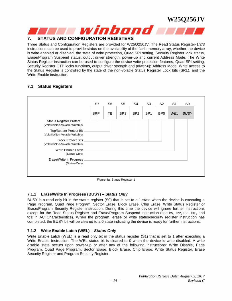
7. STATUS AND CONFIGURATION REGISTERS
Three Status and Configuration Registers are provided for W25Q256JV. The Read Status Register-1/2/3 instructions can be used to provide status on the availability of the flash memory array, whether the device is write enabled or disabled, the state of write protection, Quad SPI setting, Security Register lock status, Erase/Program Suspend status, output driver strength, power-up and current Address Mode. The Write Status Register instruction can be used to configure the device write protection features, Quad SPI setting, Security Register OTP locks functions, output driver strength and power-up Address Mode. Write access to the Status Register is controlled by the state of the non-volatile Status Register Lock bits (SRL), and the Write Enable instruction.
7.1 Status Registers
S 7 S 6 S 5 S 4 S 3 S 2 S 1 S 0
SRP TB BP 3 BP 2 BP 1 BP 0 WEL BUSY
Status Register Protect ( Volatile / Non - Volatile Writable )
Top / Bottom Protect Bit ( Volatile / Non - Volatile Writable )
Block Protect Bits ( Volatile / Non - Volatile Writable )
Write Enable Latch ( Status
s
- Only )
Erase / Write In Progress ( Status
s
- Only )
Figure 4a. Status Register-1
7.1.1 Erase/Write In Progress (BUSY) – Status Only
BUSY is a read only bit in the status register (S0) that is set to a 1 state when the device is executing a Page Program, Quad Page Program, Sector Erase, Block Erase, Chip Erase, Write Status Register or Erase/Program Security Register instruction. During this time the device will ignore further instructions except for the Read Status Register and Erase/Program Suspend instruction (see tW, tPP, tSE, tBE, and tCE in AC Characteristics). When the program, erase or write status/security register instruction has completed, the BUSY bit will be cleared to a 0 state indicating the device is ready for further instructions.
7.1.2 Write Enable Latch (WEL) – Status Only
Write Enable Latch (WEL) is a read only bit in the status register (S1) that is set to 1 after executing a Write Enable Instruction. The WEL status bit is cleared to 0 when the device is write disabled. A write disable state occurs upon power-up or after any of the following instructions: Write Disable, Page Program, Quad Page Program, Sector Erase, Block Erase, Chip Erase, Write Status Register, Erase Security Register and Program Security Register.
W25Q256JV
- 15 -
7.1.3 Block Protect Bits (BP3, BP2, BP1, BP0) – Volatile/Non-Volatile Writable
The Block Protect Bits (BP3, BP2, BP1, BP0) are non-volatile read/write bits in the status register (S5, S4, S3, and S2) that provide Write Protection control and status. Block Protect bits can be set using the Write Status Register Instruction (see tW in AC characteristics). All, none or a portion of the memory array can be protected from Program and Erase instructions (see Status Register Memory Protection table). The factory default setting for the Block Protection Bits is 0, none of the array protected.
7.1.4 Top/Bottom Block Protect (TB) – Volatile/Non-Volatile Writable
The non-volatile Top/Bottom bit (TB) controls if the Block Protect Bits (BP3, BP2, BP1, BP0) protect from the Top (TB=0) or the Bottom (TB=1) of the array as shown in the Status Register Memory Protection table. The factory default setting is TB=0. The TB bit can be set with the Write Status Register Instruction depending on the state of the WEL bits.
7.1.5 Complement Protect (CMP) – Volatile/Non-Volatile Writable
The Complement Protect bit (CMP) is a non-volatile read/write bit in the status register (S14). It is used in conjunction with TB, BP3, BP2, BP1 and BP0 bits to provide more flexibility for the array protection. Once CMP is set to 1, previous array protection set by TB, BP3, BP2, BP1 and BP0 will be reversed. For instance, when CMP=0, a top 64KB block can be protected while the rest of the array is not; when CMP=1, the top 64KB block will become unprotected while the rest of the array become read-only. Please refer to the Status Register Memory Protection table for details. The default setting is CMP=0.
W25Q256JV
Publication Release Date: August 03, 2017
- 16 - Revision G
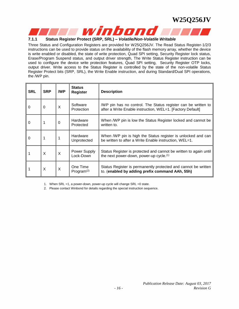
7.1.1 Status Register Protect (SRP, SRL) – Volatile/Non-Volatile Writable
Three Status and Configuration Registers are provided for W25Q256JV. The Read Status Register-1/2/3 instructions can be used to provide status on the availability of the flash memory array, whether the device is write enabled or disabled, the state of write protection, Quad SPI setting, Security Register lock status, Erase/Program Suspend status, and output driver strength, The Write Status Register instruction can be used to configure the device write protection features, Quad SPI setting, Security Register OTP locks, output driver. Write access to the Status Register is controlled by the state of the non-volatile Status Register Protect bits (SRP, SRL), the Write Enable instruction, and during Standard/Dual SPI operations, the /WP pin.
SRL SRP /WP Status
Register Description
0 0 X Software Protection
/WP pin has no control. The Status register can be written to after a Write Enable instruction, WEL=1. [Factory Default]
0 1 0 Hardware Protected
When /WP pin is low the Status Register locked and cannot be written to.
0 1 1 Hardware Unprotected
When /WP pin is high the Status register is unlocked and can be written to after a Write Enable instruction, WEL=1.
1 X X Power Supply Lock-Down
Status Register is protected and cannot be written to again until the next power-down, power-up cycle.(1)
1 X X One Time Program(2)
Status Register is permanently protected and cannot be written
to. (enabled by adding prefix command AAh, 55h)
1. When SRL =1, a power-down, power-up cycle will change SRL =0 state.
2. Please contact Winbond for details regarding the special instruction sequence.
W25Q256JV
- 17 -
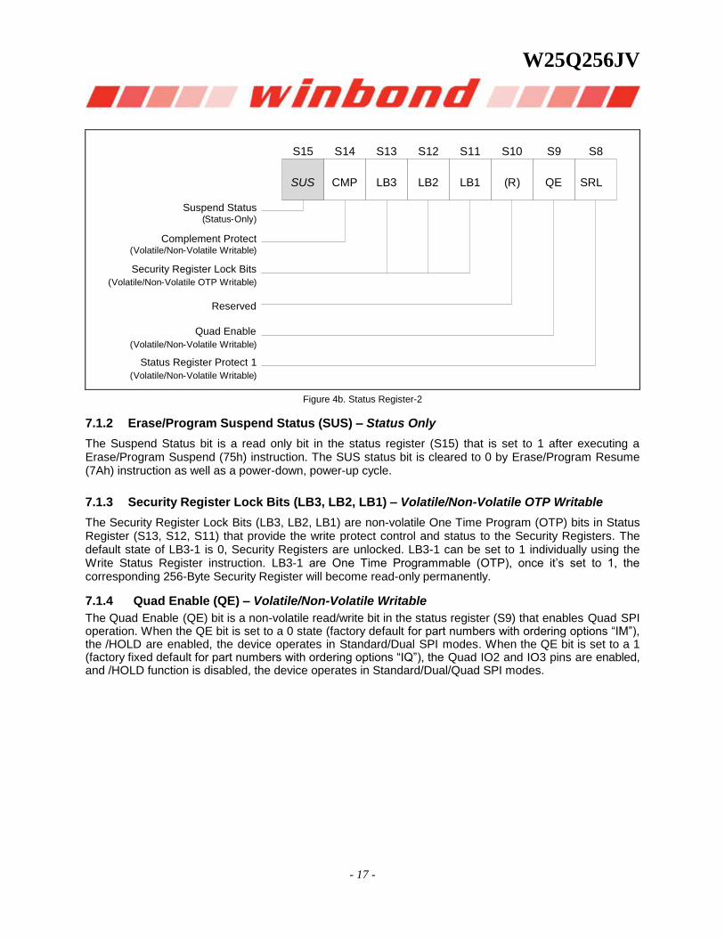
S 15 S 14 S 13 S 12 S 11 S 10 S 9 S 8
SUS CMP LB 3 LB 2 LB 1 ( R ) QE SRL
Status Register Protect 1 ( Volatile / Non - Volatile Writable )
Complement Protect ( Volatile / Non - Volatile Writable )
Security Register Lock Bits ( Volatile / Non - Volatile OTP Writable )
Reserved
Quad Enable ( Volatile / Non - Volatile Writable )
Suspend Status ( Status - Only )
Figure 4b. Status Register-2
7.1.2 Erase/Program Suspend Status (SUS) – Status Only
The Suspend Status bit is a read only bit in the status register (S15) that is set to 1 after executing a Erase/Program Suspend (75h) instruction. The SUS status bit is cleared to 0 by Erase/Program Resume (7Ah) instruction as well as a power-down, power-up cycle.
7.1.3 Security Register Lock Bits (LB3, LB2, LB1) – Volatile/Non-Volatile OTP Writable
The Security Register Lock Bits (LB3, LB2, LB1) are non-volatile One Time Program (OTP) bits in Status Register (S13, S12, S11) that provide the write protect control and status to the Security Registers. The default state of LB3-1 is 0, Security Registers are unlocked. LB3-1 can be set to 1 individually using the Write Status Register instruction. LB3-1 are One Time Programmable (OTP), once it’s set to 1, the corresponding 256-Byte Security Register will become read-only permanently.
7.1.4 Quad Enable (QE) – Volatile/Non-Volatile Writable
The Quad Enable (QE) bit is a non-volatile read/write bit in the status register (S9) that enables Quad SPI operation. When the QE bit is set to a 0 state (factory default for part numbers with ordering options “IM”), the /HOLD are enabled, the device operates in Standard/Dual SPI modes. When the QE bit is set to a 1 (factory fixed default for part numbers with ordering options “IQ”), the Quad IO2 and IO3 pins are enabled, and /HOLD function is disabled, the device operates in Standard/Dual/Quad SPI modes.
W25Q256JV
Publication Release Date: August 03, 2017
- 18 - Revision G
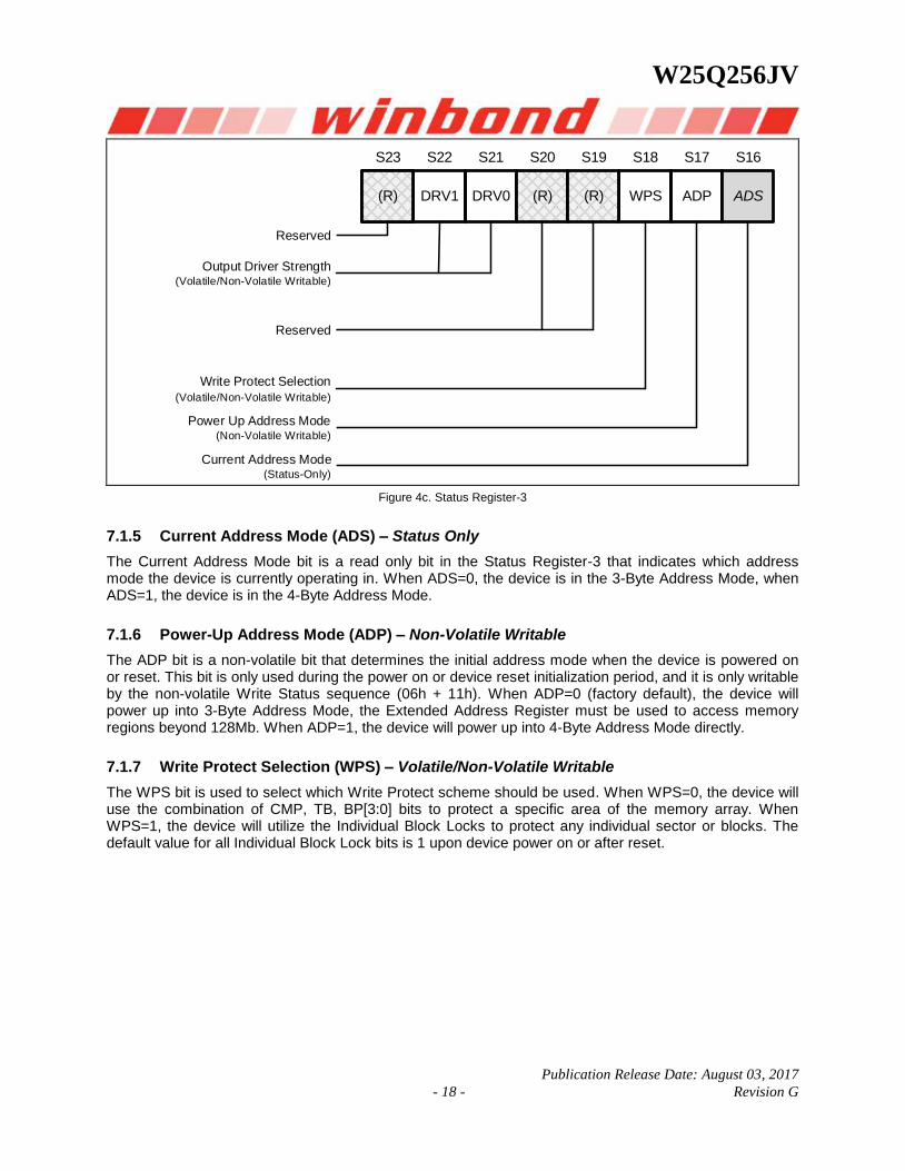
S23 S22 S21 S20 S19 S18 S17 S16
DRV1 DRV0 (R) WPS ADP ADS
Power Up Address Mode(Non-Volatile Writable)
Output Driver Strength(Volatile/Non-Volatile Writable)
Reserved
Write Protect Selection
(Volatile/Non-Volatile Writable)
Current Address Mode(Status-Only)
(R)(R)
Reserved
Figure 4c. Status Register-3
7.1.5 Current Address Mode (ADS) – Status Only
The Current Address Mode bit is a read only bit in the Status Register-3 that indicates which address mode the device is currently operating in. When ADS=0, the device is in the 3-Byte Address Mode, when ADS=1, the device is in the 4-Byte Address Mode.
7.1.6 Power-Up Address Mode (ADP) – Non-Volatile Writable
The ADP bit is a non-volatile bit that determines the initial address mode when the device is powered on or reset. This bit is only used during the power on or device reset initialization period, and it is only writable by the non-volatile Write Status sequence (06h + 11h). When ADP=0 (factory default), the device will power up into 3-Byte Address Mode, the Extended Address Register must be used to access memory regions beyond 128Mb. When ADP=1, the device will power up into 4-Byte Address Mode directly.
7.1.7 Write Protect Selection (WPS) – Volatile/Non-Volatile Writable
The WPS bit is used to select which Write Protect scheme should be used. When WPS=0, the device will use the combination of CMP, TB, BP[3:0] bits to protect a specific area of the memory array. When WPS=1, the device will utilize the Individual Block Locks to protect any individual sector or blocks. The default value for all Individual Block Lock bits is 1 upon device power on or after reset.
W25Q256JV
- 19 -
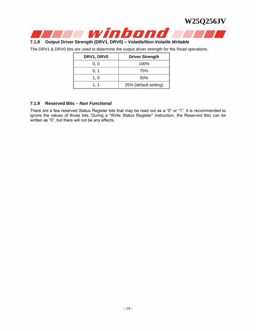
7.1.8 Output Driver Strength (DRV1, DRV0) – Volatile/Non-Volatile Writable
The DRV1 & DRV0 bits are used to determine the output driver strength for the Read operations.
DRV1, DRV0 Driver Strength
0, 0 100%
0, 1 75%
1, 0 50%
1, 1 25% (default setting)
7.1.9 Reserved Bits – Non Functional
There are a few reserved Status Register bits that may be read out as a “0” or “1”. It is recommended to ignore the values of those bits. During a “Write Status Register” instruction, the Reserved Bits can be written as “0”, but there will not be any effects.
W25Q256JV
Publication Release Date: August 03, 2017
- 20 - Revision G
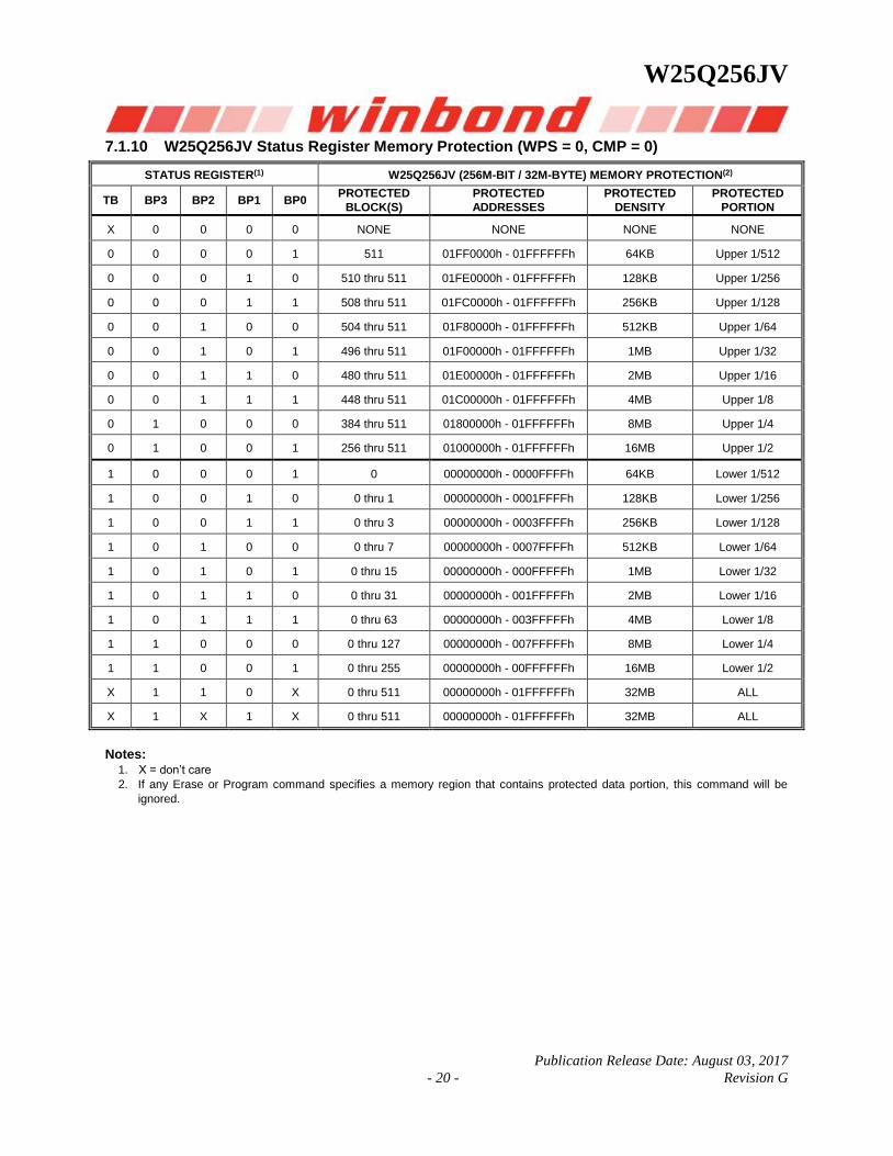
7.1.10 W25Q256JV Status Register Memory Protection (WPS = 0, CMP = 0)
STATUS REGISTER(1) W25Q256JV (256M-BIT / 32M-BYTE) MEMORY PROTECTION(2)
TB BP3 BP2 BP1 BP0 PROTECTED
BLOCK(S)
PROTECTED
ADDRESSES
PROTECTED
DENSITY
PROTECTED
PORTION
X 0 0 0 0 NONE NONE NONE NONE
0 0 0 0 1 511 01FF0000h - 01FFFFFFh 64KB Upper 1/512
0 0 0 1 0 510 thru 511 01FE0000h - 01FFFFFFh 128KB Upper 1/256
0 0 0 1 1 508 thru 511 01FC0000h - 01FFFFFFh 256KB Upper 1/128
0 0 1 0 0 504 thru 511 01F80000h - 01FFFFFFh 512KB Upper 1/64
0 0 1 0 1 496 thru 511 01F00000h - 01FFFFFFh 1MB Upper 1/32
0 0 1 1 0 480 thru 511 01E00000h - 01FFFFFFh 2MB Upper 1/16
0 0 1 1 1 448 thru 511 01C00000h - 01FFFFFFh 4MB Upper 1/8
0 1 0 0 0 384 thru 511 01800000h - 01FFFFFFh 8MB Upper 1/4
0 1 0 0 1 256 thru 511 01000000h - 01FFFFFFh 16MB Upper 1/2
1 0 0 0 1 0 00000000h - 0000FFFFh 64KB Lower 1/512
1 0 0 1 0 0 thru 1 00000000h - 0001FFFFh 128KB Lower 1/256
1 0 0 1 1 0 thru 3 00000000h - 0003FFFFh 256KB Lower 1/128
1 0 1 0 0 0 thru 7 00000000h - 0007FFFFh 512KB Lower 1/64
1 0 1 0 1 0 thru 15 00000000h - 000FFFFFh 1MB Lower 1/32
1 0 1 1 0 0 thru 31 00000000h - 001FFFFFh 2MB Lower 1/16
1 0 1 1 1 0 thru 63 00000000h - 003FFFFFh 4MB Lower 1/8
1 1 0 0 0 0 thru 127 00000000h - 007FFFFFh 8MB Lower 1/4
1 1 0 0 1 0 thru 255 00000000h - 00FFFFFFh 16MB Lower 1/2
X 1 1 0 X 0 thru 511 00000000h - 01FFFFFFh 32MB ALL
X 1 X 1 X 0 thru 511 00000000h - 01FFFFFFh 32MB ALL
Notes: 1. X = don’t care
2. If any Erase or Program command specifies a memory region that contains protected data portion, this command will be
ignored.
W25Q256JV
- 21 -
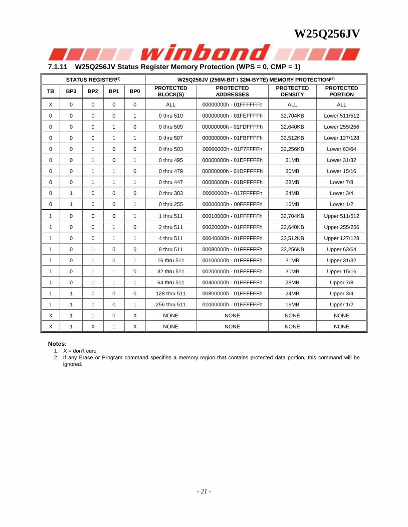
7.1.11 W25Q256JV Status Register Memory Protection (WPS = 0, CMP = 1)
STATUS REGISTER(1) W25Q256JV (256M-BIT / 32M-BYTE) MEMORY PROTECTION(2)
TB BP3 BP2 BP1 BP0 PROTECTED
BLOCK(S)
PROTECTED
ADDRESSES
PROTECTED
DENSITY
PROTECTED
PORTION
X 0 0 0 0 ALL 00000000h - 01FFFFFFh ALL ALL
0 0 0 0 1 0 thru 510 00000000h - 01FEFFFFh 32,704KB Lower 511/512
0 0 0 1 0 0 thru 509 00000000h - 01FDFFFFh 32,640KB Lower 255/256
0 0 0 1 1 0 thru 507 00000000h - 01FBFFFFh 32,512KB Lower 127/128
0 0 1 0 0 0 thru 503 00000000h - 01F7FFFFh 32,256KB Lower 63/64
0 0 1 0 1 0 thru 495 00000000h - 01EFFFFFh 31MB Lower 31/32
0 0 1 1 0 0 thru 479 00000000h - 01DFFFFFh 30MB Lower 15/16
0 0 1 1 1 0 thru 447 00000000h - 01BFFFFFh 28MB Lower 7/8
0 1 0 0 0 0 thru 383 00000000h - 017FFFFFh 24MB Lower 3/4
0 1 0 0 1 0 thru 255 00000000h - 00FFFFFFh 16MB Lower 1/2
1 0 0 0 1 1 thru 511 00010000h - 01FFFFFFh 32,704KB Upper 511/512
1 0 0 1 0 2 thru 511 00020000h - 01FFFFFFh 32,640KB Upper 255/256
1 0 0 1 1 4 thru 511 00040000h - 01FFFFFFh 32,512KB Upper 127/128
1 0 1 0 0 8 thru 511 00080000h - 01FFFFFFh 32,256KB Upper 63/64
1 0 1 0 1 16 thru 511 00100000h - 01FFFFFFh 31MB Upper 31/32
1 0 1 1 0 32 thru 511 00200000h - 01FFFFFFh 30MB Upper 15/16
1 0 1 1 1 64 thru 511 00400000h - 01FFFFFFh 28MB Upper 7/8
1 1 0 0 0 128 thru 511 00800000h - 01FFFFFFh 24MB Upper 3/4
1 1 0 0 1 256 thru 511 01000000h - 01FFFFFFh 16MB Upper 1/2
X 1 1 0 X NONE NONE NONE NONE
X 1 X 1 X NONE NONE NONE NONE
Notes: 1. X = don’t care
2. If any Erase or Program command specifies a memory region that contains protected data portion, this command will be
ignored.
W25Q256JV
Publication Release Date: August 03, 2017
- 22 - Revision G
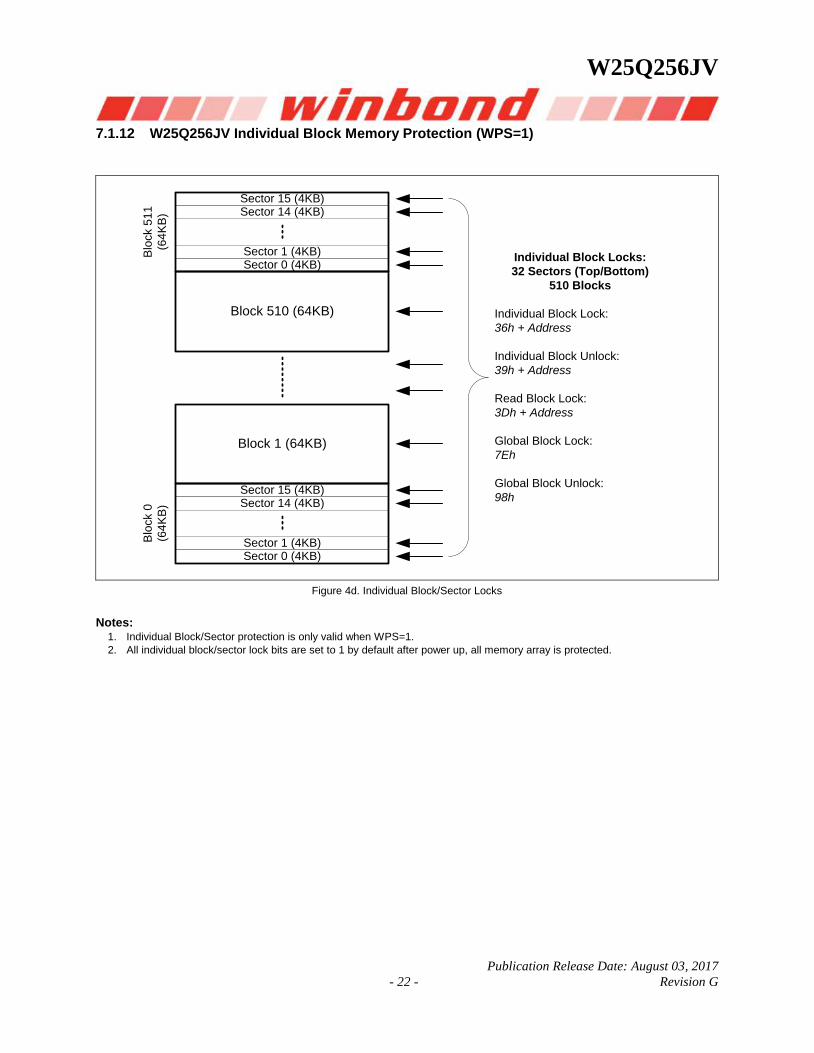
7.1.12 W25Q256JV Individual Block Memory Protection (WPS=1)
Sector 0 (4KB)Sector 1 (4KB)
Sector 14 (4KB)Sector 15 (4KB)
Block 1 (64KB)
Block 510 (64KB)
Sector 0 (4KB)Sector 1 (4KB)
Sector 14 (4KB)Sector 15 (4KB)
Blo
ck 0
(64
KB
)
Blo
ck 5
11
(64
KB
)
Individual Block Locks:
32 Sectors (Top/Bottom)
510 Blocks
Individual Block Lock:
36h + Address
Individual Block Unlock:
39h + Address
Read Block Lock:
3Dh + Address
Global Block Lock:
7Eh
Global Block Unlock:
98h
Figure 4d. Individual Block/Sector Locks
Notes: 1. Individual Block/Sector protection is only valid when WPS=1.
2. All individual block/sector lock bits are set to 1 by default after power up, all memory array is protected.
W25Q256JV
- 23 -
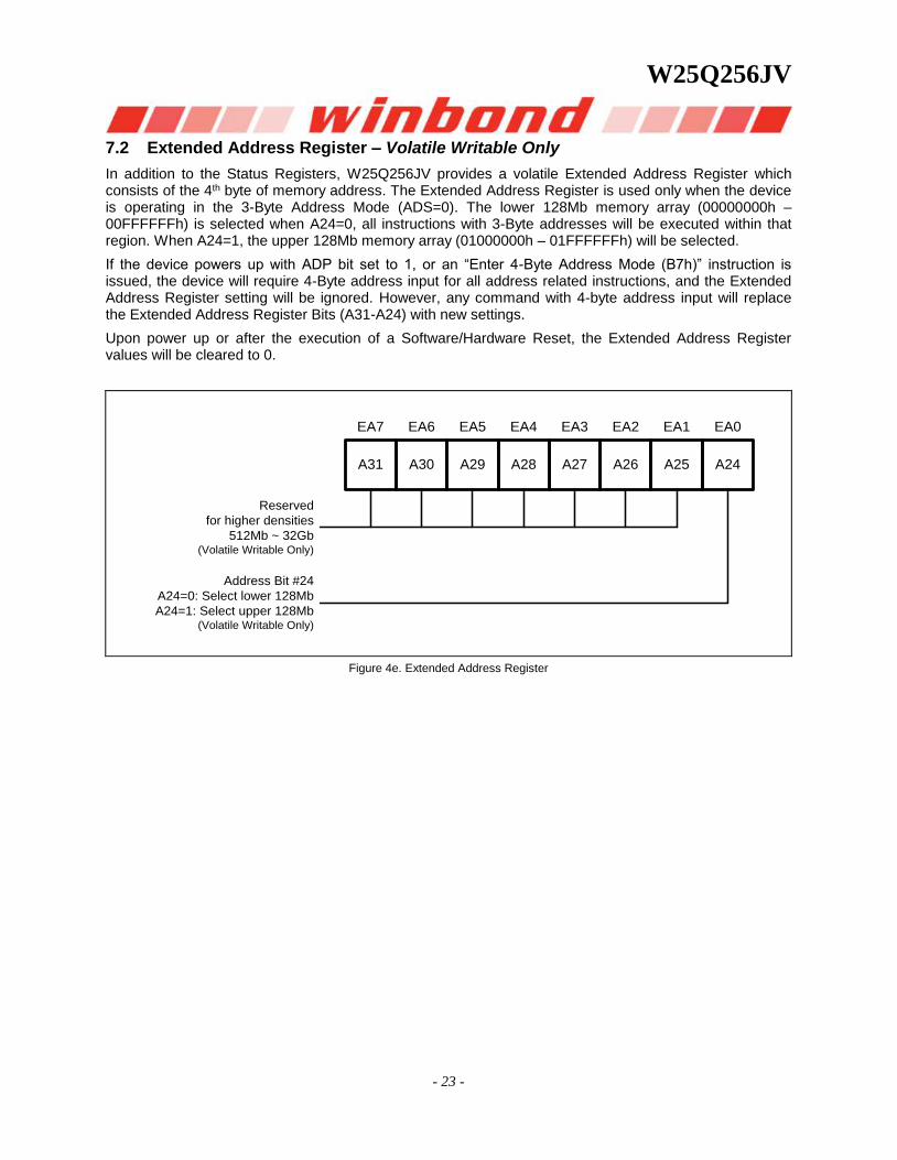
7.2 Extended Address Register – Volatile Writable Only
In addition to the Status Registers, W25Q256JV provides a volatile Extended Address Register which consists of the 4th byte of memory address. The Extended Address Register is used only when the device is operating in the 3-Byte Address Mode (ADS=0). The lower 128Mb memory array (00000000h – 00FFFFFFh) is selected when A24=0, all instructions with 3-Byte addresses will be executed within that region. When A24=1, the upper 128Mb memory array (01000000h – 01FFFFFFh) will be selected.
If the device powers up with ADP bit set to 1, or an “Enter 4-Byte Address Mode (B7h)” instruction is issued, the device will require 4-Byte address input for all address related instructions, and the Extended Address Register setting will be ignored. However, any command with 4-byte address input will replace the Extended Address Register Bits (A31-A24) with new settings.
Upon power up or after the execution of a Software/Hardware Reset, the Extended Address Register values will be cleared to 0.
EA7 EA6 EA5 EA4 EA3 EA2 EA1 EA0
A31 A30 A29 A28 A27 A26 A25 A24
Reserved
for higher densities
512Mb ~ 32Gb(Volatile Writable Only)
Address Bit #24
A24=0: Select lower 128Mb
A24=1: Select upper 128Mb(Volatile Writable Only)
Figure 4e. Extended Address Register
W25Q256JV
Publication Release Date: August 03, 2017
- 24 - Revision G
8. INSTRUCTIONS
The Standard/Dual/Quad SPI instruction set of the W25Q256JV consists of 48 basic instructions that are fully controlled through the SPI bus (see Instruction Set Table1-4). Instructions are initiated with the falling edge of Chip Select (/CS). The first byte of data clocked into the DI input provides the instruction code. Data on the DI input is sampled on the rising edge of clock with most significant bit (MSB) first.
Instructions vary in length from a single byte to several bytes and may be followed by address bytes, data bytes, dummy bytes (don’t care), and in some cases, a combination. Instructions are completed with the rising edge of edge /CS. Clock relative timing diagrams for each instruction are included in Figures 5 through 57. All read instructions can be completed after any clocked bit. However, all instructions that Write, Program or Erase must complete on a byte boundary (/CS driven high after a full 8-bits have been clocked) otherwise the instruction will be ignored. This feature further protects the device from inadvertent writes. Additionally, while the memory is being programmed or erased, or when the Status Register is being written, all instructions except for Read Status Register will be ignored until the program or erase cycle has completed.
8.1 Device ID and Instruction Set Tables
8.1.1 Manufacturer and Device Identification
MANUFACTURER ID (MF7 - MF0)
Winbond Serial Flash EFh
Device ID (ID7 - ID0) (ID15 - ID0)
Instruction ABh, 90h, 92h, 94h 9Fh
W25Q256JV-IQ 18h 4019h
W25Q256JV-IM* 18h 7019h
Note: For DTR, QPI supporting, please refer to W25Q256JV DTR datasheet.
W25Q256JV
- 25 -
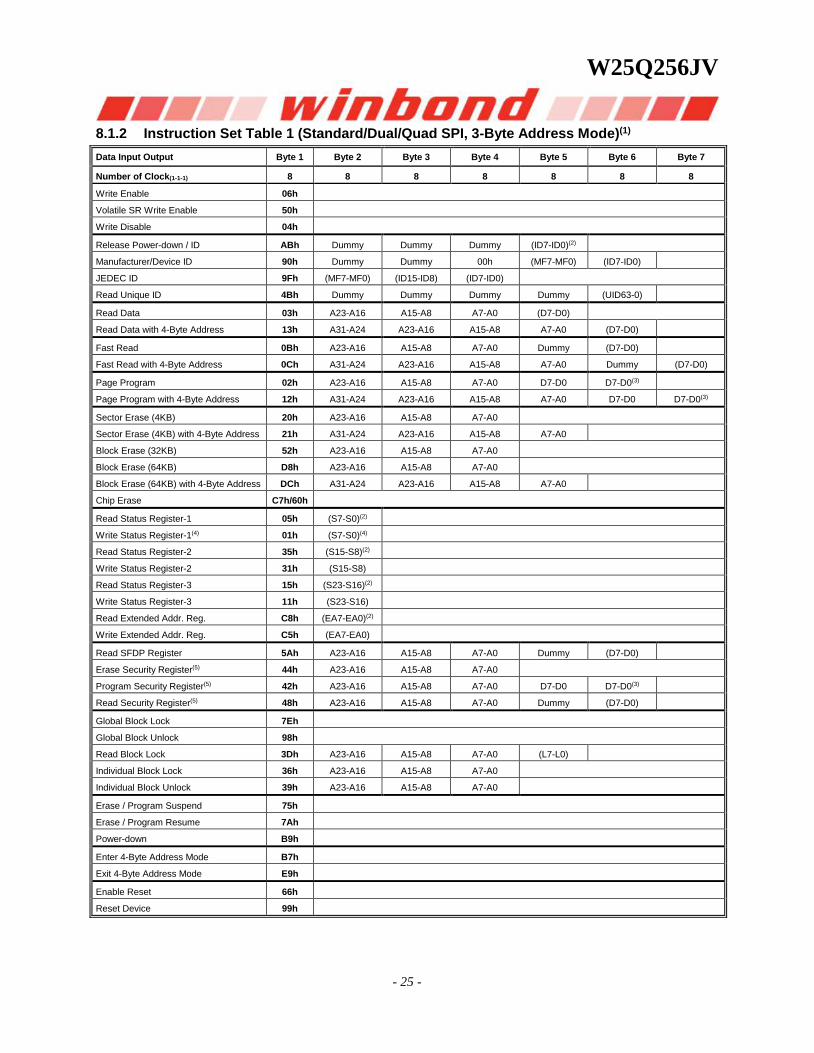
8.1.2 Instruction Set Table 1 (Standard/Dual/Quad SPI, 3-Byte Address Mode)(1)
Data Input Output Byte 1 Byte 2 Byte 3 Byte 4 Byte 5 Byte 6 Byte 7
Number of Clock(1-1-1) 8 8 8 8 8 8 8
Write Enable 06h
Volatile SR Write Enable 50h
Write Disable 04h
Release Power-down / ID ABh Dummy Dummy Dummy (ID7-ID0)(2)
Manufacturer/Device ID 90h Dummy Dummy 00h (MF7-MF0) (ID7-ID0)
JEDEC ID 9Fh (MF7-MF0) (ID15-ID8) (ID7-ID0)
Read Unique ID 4Bh Dummy Dummy Dummy Dummy (UID63-0)
Read Data 03h A23-A16 A15-A8 A7-A0 (D7-D0)
Read Data with 4-Byte Address 13h A31-A24 A23-A16 A15-A8 A7-A0 (D7-D0)
Fast Read 0Bh A23-A16 A15-A8 A7-A0 Dummy (D7-D0)
Fast Read with 4-Byte Address 0Ch A31-A24 A23-A16 A15-A8 A7-A0 Dummy (D7-D0)
Page Program 02h A23-A16 A15-A8 A7-A0 D7-D0 D7-D0(3)
Page Program with 4-Byte Address 12h A31-A24 A23-A16 A15-A8 A7-A0 D7-D0 D7-D0(3)
Sector Erase (4KB) 20h A23-A16 A15-A8 A7-A0
Sector Erase (4KB) with 4-Byte Address 21h A31-A24 A23-A16 A15-A8 A7-A0
Block Erase (32KB) 52h A23-A16 A15-A8 A7-A0
Block Erase (64KB) D8h A23-A16 A15-A8 A7-A0
Block Erase (64KB) with 4-Byte Address DCh A31-A24 A23-A16 A15-A8 A7-A0
Chip Erase C7h/60h
Read Status Register-1 05h (S7-S0)(2)
Write Status Register-1(4) 01h (S7-S0)(4)
Read Status Register-2 35h (S15-S8)(2)
Write Status Register-2 31h (S15-S8)
Read Status Register-3 15h (S23-S16)(2)
Write Status Register-3 11h (S23-S16)
Read Extended Addr. Reg. C8h (EA7-EA0)(2)
Write Extended Addr. Reg. C5h (EA7-EA0)
Read SFDP Register 5Ah A23-A16 A15-A8 A7-A0 Dummy (D7-D0)
Erase Security Register(5) 44h A23-A16 A15-A8 A7-A0
Program Security Register(5) 42h A23-A16 A15-A8 A7-A0 D7-D0 D7-D0(3)
Read Security Register(5) 48h A23-A16 A15-A8 A7-A0 Dummy (D7-D0)
Global Block Lock 7Eh
Global Block Unlock 98h
Read Block Lock 3Dh A23-A16 A15-A8 A7-A0 (L7-L0)
Individual Block Lock 36h A23-A16 A15-A8 A7-A0
Individual Block Unlock 39h A23-A16 A15-A8 A7-A0
Erase / Program Suspend 75h
Erase / Program Resume 7Ah
Power-down B9h
Enter 4-Byte Address Mode B7h
Exit 4-Byte Address Mode E9h
Enable Reset 66h
Reset Device 99h
W25Q256JV
Publication Release Date: August 03, 2017
- 26 - Revision G
8.1.3 Instruction Set Table 2 (Dual/Quad SPI Instructions,3-Byte Address Mode)
Data Input Output Byte 1 Byte 2 Byte 3 Byte 4 Byte 5 Byte 6 Byte 7 Byte 8 Byte 9 Byte 10
Number of Clock(1-1-2) 8 8 8 8 4 4 4 4 4 4
Fast Read Dual Output 3Bh A23-A16 A15-A8 A7-A0 Dummy Dummy (D7-D0)(7) …
Fast Read Dual Output with 4-Byte Address
3Ch A31-A24 A23-A16 A15-A8 A7-A0 Dummy Dummy (D7-D0)(7) …
Number of Clock(1-2-2) 8 4 4 4 4 4 4 4 4 4
Mftr./Device ID Dual I/O 92h A23-A16 A15-A8 0 Dummy(11) (MF7-MF0) (ID7-ID0)
Fast Read Dual I/O BBh A23-A16 A15-A8 A7-A0 Dummy(11) (D7-D0) …
Fast Read Dual I/O with 4-Byte Address
BCh A31-A24 A23-A16 A15-A8 A7-A0 Dummy(11) (D7-D0) …
Number of Clock(1-1-4) 8 8 8 8 2 2 2 2 2 2
Quad Input Page Program
32h A23-A16 A15-A8 A7-A0 (D7-D0)(9) (D7-D0)(3) …
Quad Page Program with 4-Byte Address
34h A31-A24 A23-A16 A15-A8 A7-A0 D7-D0 … …
Fast Read Quad Output 6Bh A23-A16 A15-A8 A7-A0 Dummy Dummy Dummy Dummy (D7-D0)(9) …
Number of Clock(1-1-4) 8 8 8 8 8 2 2 2 2 2
Fast Read Quad Output with 4-Byte Address
6Ch A31-A24 A23-A16 A15-A8 A7-A0 Dummy Dummy Dummy Dummy (D7-D0)(9)
Number of Clock(1-4-4) 8 2 2 2 2 2 2 2 2 2
Mftr./Device ID Quad I/O 94h A23-A16 A15-A8 0 Dummy(11) Dummy Dummy (MF7-MF0) (ID7-ID0)
Fast Read Quad I/O EBh A23-A16 A15-A8 A7-A0 Dummy(11) Dummy Dummy (D7-D0) …
Fast Read Quad I/O with 4-Byte Address
ECh A31-A24 A23-A16 A15-A8 A7-A0f Dummy(11) Dummy Dummy (D7-D0) …
Set Burst with Wrap 77h Dummy Dummy Dummy W7-W0
W25Q256JV
- 27 -
8.1.4 Instruction Set Table 3 (Standard SPI, 4-Byte Address Mode)(1)
Data Input Output Byte 1 Byte 2 Byte 3 Byte 4 Byte 5 Byte 6 Byte 7
Number of Clock(1-1-1) 8 8 8 8 8 8 8
Write Enable 06h
Volatile SR Write Enable 50h
Write Disable 04h
Release Power-down / ID ABh Dummy Dummy Dummy (ID7-ID0)(2)
Manufacturer/Device ID 90h Dummy Dummy 00h (MF7-MF0) (ID7-ID0)
JEDEC ID 9Fh (MF7-MF0) (ID15-ID8) (ID7-ID0)
Read Unique ID 4Bh Dummy Dummy Dummy Dummy Dummy (UID63-0)
Read Data 03h A31-A24 A23-A16 A15-A8 A7-A0 (D7-D0)
Read Data with 4-Byte Address 13h A31-A24 A23-A16 A15-A8 A7-A0 (D7-D0)
Fast Read 0Bh A31-A24 A23-A16 A15-A8 A7-A0 Dummy (D7-D0)
Fast Read with 4-Byte Address 0Ch A31-A24 A23-A16 A15-A8 A7-A0 Dummy (D7-D0)
Page Program 02h A31-A24 A23-A16 A15-A8 A7-A0 D7-D0 D7-D0(3)
Page Program with 4-Byte Address 12h A31-A24 A23-A16 A15-A8 A7-A0 D7-D0 D7-D0(3)
Sector Erase (4KB) 20h A31-A24 A23-A16 A15-A8 A7-A0
Sector Erase (4KB) with 4-Byte Address 21h A31-A24 A23-A16 A15-A8 A7-A0
Block Erase (32KB) 52h A31-A24 A23-A16 A15-A8 A7-A0
Block Erase (64KB) D8h A31-A24 A23-A16 A15-A8 A7-A0
Block Erase (64KB) with 4-Byte Address DCh A31-A24 A23-A16 A15-A8 A7-A0
Chip Erase C7h/60h
Read Status Register-1 05h (S7-S0)(2)
Write Status Register-1(4) 01h (S7-S0)(4)
Read Status Register-2 35h (S15-S8)(2)
Write Status Register-2 31h (S15-S8)
Read Status Register-3 15h (S23-S16)(2)
Write Status Register-3 11h (S23-S16)
Read Extended Addr. Reg. C8h (EA7-EA0)(2)
Write Extended Addr. Reg. C5h (EA7-EA0)
Read SFDP Register 5Ah A23-A16 A15-A8 A7-A0 Dummy (D7-D0)
Erase Security Register(5) 44h A31-A24 A23-A16 A15-A8 A7-A0
Program Security Register(5) 42h A31-A24 A23-A16 A15-A8 A7-A0 D7-D0 D7-D0(3)
Read Security Register(5) 48h A31-A24 A23-A16 A15-A8 A7-A0 Dummy (D7-D0)
Global Block Lock 7Eh
Global Block Unlock 98h
Read Block Lock 3Dh A31-A24 A23-A16 A15-A8 A7-A0 (L7-L0)
Individual Block Lock 36h A31-A24 A23-A16 A15-A8 A7-A0
Individual Block Unlock 39h A31-A24 A23-A16 A15-A8 A7-A0
Erase / Program Suspend 75h
Erase / Program Resume 7Ah
Power-down B9h
Enter 4-Byte Address Mode B7h
Exit 4-Byte Address Mode E9h
Enable Reset 66h
Reset Device 99h
W25Q256JV
Publication Release Date: August 03, 2017
- 28 - Revision G
8.1.5 Instruction Set Table 4 (Dual/Quad SPI Instructions, 4-Byte Address Mode)
Data Input Output Byte 1 Byte 2 Byte 3 Byte 4 Byte 5 Byte 6 Byte 7 Byte 8 Byte9
Number of Clock(1-1-2) 8 8 8 8 8 8 4 4
Fast Read Dual Output 3Bh A31-A24 A23-A16 A15-A8 A7-A0 Dummy (D7-D0,…)(7)
Fast Read Dual Output with 4-Byte Address 3Ch A31-A24 A23-A16 A15-A8 A7-A0 Dummy (D7-D0,…)(7)
Number of Clock(1-2-2) 8 4 4 4 4 4 4 4
Mftr./Device ID Dual I/O 92h A31-A24 A23-A16 A15-A8 00 Dummy(11) (MF7-MF0) (ID7-ID0)
Fast Read Dual I/O BBh A31-A24 A23-A16 A15-A8 A7-A0 Dummy(11) (D7-D0)
Fast Read Dual I/O with 4-Byte Address BCh A31-A24 A23-A16 A15-A8 A7-A0 Dummy(11) (D7-D0)
Number of Clock(1-1-4) 8 8 8 8 8 4 4 4
Quad Input Page Program 32h A31-A24 A23-A16 A15-A8 A7-A0 (D7-D0)(9) (D7-D0)(3)..
Quad Page Program with 4-Byte Address 34h A31-A24 A23-A16 A15-A8 A7-A0 D7-D0 D7-D0 D7-D0 D7-D0
Fast Read Quad Output 6Bh A31-A24 A23-A16 A15-A8 A7-A0 Dummy Dummy (D7-D0)(9)
Fast Read Quad Output with 4-Byte Address 6Ch A31-A24 A23-A16 A15-A8 A7-A0 Dummy Dummy (D7-D0)(9)
Number of Clock(1-4-4) 8 2 2 2 2 2 4 2 2
Mftr./Device ID Quad I/O 94h A31-A24 A23-A16 A15-A8 00 Dummy(11) Dummy (MF7-MF0) (ID7-ID0)
Fast Read Quad I/O EBh A31-A24 A23-A16 A15-A8 A7-A0 Dummy(11) Dummy (D7-D0)
Fast Read Quad I/O with 4-Byte Address ECh A31-A24 A23-A16 A15-A8 A7-A0 Dummy(11) Dummy (D7-D0)
Set Burst with Wrap 77h Dummy Dummy Dummy Dummy W7-W0
W25Q256JV
- 29 -
Notes:
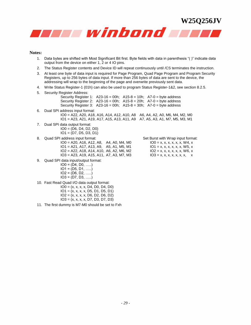
1. Data bytes are shifted with Most Significant Bit first. Byte fields with data in parenthesis “( )” indicate data output from the device on either 1, 2 or 4 IO pins.
2. The Status Register contents and Device ID will repeat continuously until /CS terminates the instruction.
3. At least one byte of data input is required for Page Program, Quad Page Program and Program Security Registers, up to 256 bytes of data input. If more than 256 bytes of data are sent to the device, the addressing will wrap to the beginning of the page and overwrite previously sent data.
4. Write Status Register-1 (01h) can also be used to program Status Register-1&2, see section 8.2.5.
5. Security Register Address: Security Register 1: A23-16 = 00h; A15-8 = 10h; A7-0 = byte address Security Register 2: A23-16 = 00h; A15-8 = 20h; A7-0 = byte address Security Register 3: A23-16 = 00h; A15-8 = 30h; A7-0 = byte address
6. Dual SPI address input format: IO0 = A22, A20, A18, A16, A14, A12, A10, A8 A6, A4, A2, A0, M6, M4, M2, M0 IO1 = A23, A21, A19, A17, A15, A13, A11, A9 A7, A5, A3, A1, M7, M5, M3, M1
7. Dual SPI data output format: IO0 = (D6, D4, D2, D0) IO1 = (D7, D5, D3, D1)
8. Quad SPI address input format: Set Burst with Wrap input format: IO0 = A20, A16, A12, A8, A4, A0, M4, M0 IO0 = x, x, x, x, x, x, W4, x IO1 = A21, A17, A13, A9, A5, A1, M5, M1 IO1 = x, x, x, x, x, x, W5, x IO2 = A22, A18, A14, A10, A6, A2, M6, M2 IO2 = x, x, x, x, x, x, W6, x IO3 = A23, A19, A15, A11, A7, A3, M7, M3 IO3 = x, x, x, x, x, x, x, x
9. Quad SPI data input/output format: IO0 = (D4, D0, …..) IO1 = (D5, D1, …..) IO2 = (D6, D2, …..) IO3 = (D7, D3, …..)
10. Fast Read Quad I/O data output format: IO0 = (x, x, x, x, D4, D0, D4, D0) IO1 = (x, x, x, x, D5, D1, D5, D1) IO2 = (x, x, x, x, D6, D2, D6, D2) IO3 = (x, x, x, x, D7, D3, D7, D3)
11. The first dummy is M7-M0 should be set to Fxh
W25Q256JV
Publication Release Date: August 03, 2017
- 30 - Revision G
8.2 Instruction Descriptions
8.2.1 Write Enable (06h)
The Write Enable instruction (Figure 5) sets the Write Enable Latch (WEL) bit in the Status Register to a 1. The WEL bit must be set prior to every Page Program, Quad Page Program, Sector Erase, Block Erase, Chip Erase, Write Status Register and Erase/Program Security Registers instruction. The Write Enable instruction is entered by driving /CS low, shifting the instruction code “06h” into the Data Input (DI) pin on the rising edge of CLK, and then driving /CS high.
/CS
CLK
DI
(IO0)
DO
(IO1)
Mode 0
Mode 3 0 1 2 3 4 5 6 7
Mode 0
Mode 3
Instruction (06h)
High Impedance
Figure 5. Write Enable Instruction
8.2.2 Write Enable for Volatile Status Register (50h)
The non-volatile Status Register bits described in section 7.1 can also be written to as volatile bits. This gives more flexibility to change the system configuration and memory protection schemes quickly without waiting for the typical non-volatile bit write cycles or affecting the endurance of the Status Register non-volatile bits. To write the volatile values into the Status Register bits, the Write Enable for Volatile Status Register (50h) instruction must be issued prior to a Write Status Register (01h) instruction. Write Enable for Volatile Status Register instruction (Figure 6) will not set the Write Enable Latch (WEL) bit, it is only valid for the Write Status Register instruction to change the volatile Status Register bit values.
/CS
CLK
DI
(IO0)
DO
(IO1)
Mode 0
Mode 3 0 1 2 3 4 5 6 7
Mode 0
Mode 3
Instruction (50h)
High Impedance
Figure 6. Write Enable for Volatile Status Register Instruction
W25Q256JV
- 31 -
8.2.3 Write Disable (04h)
The Write Disable instruction (Figure 7) resets the Write Enable Latch (WEL) bit in the Status Register to a 0. The Write Disable instruction is entered by driving /CS low, shifting the instruction code “04h” into the DI pin and then driving /CS high. Note that the WEL bit is automatically reset after Power-up and upon completion of the Write Status Register, Erase/Program Security Registers, Page Program, Quad Page Program, Sector Erase, Block Erase, Chip Erase and Reset instructions.
/CS
CLK
DI
(IO0)
DO
(IO1)
Mode 0
Mode 3 0 1 2 3 4 5 6 7
Mode 0
Mode 3
Instruction (04h)
High Impedance
Figure 7. Write Disable Instruction for SPI Mode
8.2.4 Read Status Register-1 (05h), Status Register-2 (35h) & Status Register-3 (15h)
The Read Status Register instructions allow the 8-bit Status Registers to be read. The instruction is entered by driving /CS low and shifting the instruction code “05h” for Status Register-1, “35h” for Status Register-2 or “15h” for Status Register-3 into the DI pin on the rising edge of CLK. The status register bits are then shifted out on the DO pin at the falling edge of CLK with most significant bit (MSB) first as shown in Figure 8. Refer to section 7.1 for Status Register descriptions.
The Read Status Register instruction may be used at any time, even while a Program, Erase or Write Status Register cycle is in progress. This allows the BUSY status bit to be checked to determine when the cycle is complete and if the device can accept another instruction. The Status Register can be read continuously, as shown in Figure 8. The instruction is completed by driving /CS high.
/CS
CLK
DI
(IO0)
DO
(IO1)
Mode 0
Mode 3 0 1 2 3 4 5 6 7
Instruction (05h/35h/15h)
High Impedance
8 9 10 11 12 13 14 15 16 17 18 19 20 21 22 23
7 6 5 4 3 2 1 0 7 6 5 4 3 2 1 0 7
Status Register-1/2/3 out Status Register-1/2/3 out
* *= MSB*
Figure 8. Read Status Register Instruction
W25Q256JV
Publication Release Date: August 03, 2017
- 32 - Revision G
8.2.5 Write Status Register-1 (01h), Status Register-2 (31h) & Status Register-3 (11h)
The Write Status Register instruction allows the Status Registers to be written. The writable Status Register bits include: TB, BP[3:0] in Status Register-1; CMP, LB[3:1], QE, SRL in Status Register-2;, DRV1, DRV0, WPS & ADP in Status Register-3. All other Status Register bit locations are read-only and will not be affected by the Write Status Register instruction. LB[3:1] are non-volatile OTP bits, once it is set to 1, it cannot be cleared to 0.
To write non-volatile Status Register bits, a standard Write Enable (06h) instruction must previously have been executed for the device to accept the Write Status Register instruction (Status Register bit WEL must equal 1). Once write enabled, the instruction is entered by driving /CS low, sending the instruction code “01h/31h/11h”, and then writing the status register data byte as illustrated in Figure 9a.
To write volatile Status Register bits, a Write Enable for Volatile Status Register (50h) instruction must have been executed prior to the Write Status Register instruction (Status Register bit WEL remains 0). However, SRL and LB[3:1] cannot be changed from “1” to “0” because of the OTP protection for these bits. Upon power off or the execution of a Software/Hardware Reset, the volatile Status Register bit values will be lost, and the non-volatile Status Register bit values will be restored.
During non-volatile Status Register write operation (06h combined with 01h/31h/11h), after /CS is driven high, the self-timed Write Status Register cycle will commence for a time duration of tW (See AC Characteristics). While the Write Status Register cycle is in progress, the Read Status Register instruction may still be accessed to check the status of the BUSY bit. The BUSY bit is a 1 during the Write Status Register cycle and a 0 when the cycle is finished and ready to accept other instructions again. After the Write Status Register cycle has finished, the Write Enable Latch (WEL) bit in the Status Register will be cleared to 0.
During volatile Status Register write operation (50h combined with 01h/31h/11h), after /CS is driven high, the Status Register bits will be refreshed to the new values within the time period of tSHSL2 (See AC Characteristics). BUSY bit will remain 0 during the Status Register bit refresh period.
Refer to section 7.1 for Status Register descriptions.
/CS
CLK
DI
(IO0)
DO
(IO1)
Mode 0
Mode 3 0 1 2 3 4 5 6 7
Instruction
(01h/31h/11h)
High Impedance
8 9 10 11 12 13 14 15
7 6 5 4 3 2 1 0
Register-1/2/3 in
Mode 0
Mode 3
*
= MSB*
Figure 9a. Write Status Register-1/2/3 Instruction
W25Q256JV
- 33 -
The W25Q256JV is also backward compatible to Winbond’s previous generations of serial flash memories, in which the Status Register-1&2 can be written using a single “Write Status Register-1 (01h)” command. To complete the Write Status Register-1&2 instruction, the /CS pin must be driven high after the sixteenth bit of data that is clocked in as shown in Figure 9b. If /CS is driven high after the eighth clock, the Write Status Register-1 (01h) instruction will only program the Status Register-1, the Status Register-2 will not be affected (Previous generations will clear CMP and QE bits).
/CS
CLK
DI
(IO0)
DO
(IO1)
Mode 0
Mode 3 0 1 2 3 4 5 6 7
Instruction (01h)
High Impedance
8 9 10 11 12 13 14 15 16 17 18 19 20 21 22 23
7 6 5 4 3 2 1 0 15 14 13 12 11 10 9 8
Status Register 1 in Status Register 2 in
Mode 0
Mode 3
* *
= MSB*
Figure 9b. Write Status Register-1/2 Instruction
W25Q256JV
Publication Release Date: August 03, 2017
- 34 - Revision G
8.2.6 Read Extended Address Register (C8h)
When the device is in the 3-Byte Address Mode, the Extended Address Register is used as the 4th address byte A[31:24] to access memory regions beyond 128Mb. The Read Extended Address Register instruction is entered by driving /CS low and shifting the instruction code “C8h” into the DI pin on the rising edge of CLK. The Extended Address Register bits are then shifted out on the DO pin at the falling edge of CLK with most significant bit (MSB) first as shown in Figure 10.
When the device is in the 4-Byte Address Mode, the Extended Address Register is not used.
/CS
CLK
DI
(IO0)
DO
(IO1)
Mode 0
Mode 3 0 1 2 3 4 5 6 7
Instruction (C8h)
High Impedance
8 9 10 11 12 13 14 15 16 17 18 19 20 21 22 23
7 6 5 4 3 2 1 0 7 6 5 4 3 2 1 0 7
Extended Addr. Reg. Out Extended Addr. Reg. Out
* *= MSB*
Figure 10a. Read Extended Address Register Instruction
W25Q256JV
- 35 -
8.2.7 Write Extended Address Register (C5h)
The Extended Address Register is a volatile register that stores the 4th byte address (A31-A24) when the device is operating in the 3-Byte Address Mode (ADS=0). To write the Extended Address Register bits, a Write Enable (06h) instruction must previously have been executed for the device to accept the Write Extended Address Register instruction (Status Register bit WEL must equal 1). Once write enabled, the instruction is entered by driving /CS low, sending the instruction code “C5h”, and then writing the Extended Address Register data byte as illustrated in Figure 11.
Upon power up or the execution of a Software/Hardware Reset, the Extended Address Register bit values will be cleared to 0.
The Extended Address Register is only effective when the device is in the 3-Byte Address Mode. When the device operates in the 4-Byte Address Mode (ADS=1), any command with address input of A31-A24 will replace the Extended Address Register values. It is recommended to check and update the Extended Address Register if necessary when the device is switched from 4-Byte to 3-Byte Address Mode.
/CS
CLK
DI
(IO0)
DO
(IO1)
Mode 0
Mode 3 0 1 2 3 4 5 6 7
Instruction (C5h)
High Impedance
8 9 10 11 12 13 14 15
7 6 5 4 3 2 1 0
Ext. Add. Reg in
Mode 0
Mode 3
*
= MSB*
Figure 11. Write Extended Address Register Instruction
W25Q256JV
Publication Release Date: August 03, 2017
- 36 - Revision G
8.2.8 Enter 4-Byte Address Mode (B7h)
The Enter 4-Byte Address Mode instruction (Figure 12) will allow 32-bit address (A31-A0) to be used to access the memory array beyond 128Mb. The Enter 4-Byte Address Mode instruction is entered by driving /CS low, shifting the instruction code “B7h” into the DI pin and then driving /CS high.
/CS
CLK
DI
(IO0)
DO
(IO1)
Mode 0
Mode 3 0 1 2 3 4 5 6 7
Mode 0
Mode 3
Instruction (B7h)
High Impedance
Figure 12. Enter 4-Byte Address Mode instruction
8.2.9 Exit 4-Byte Address Mode (E9h)
In order to be backward compatible, the Exit 4-Byte Address Mode instruction (Figure 13) will only allow 24-bit address (A23-A0) to be used to access the memory array up to 128Mb. The Extended Address Register must be used to access the memory array beyond 128Mb. The Exit 4-Byte Address Mode instruction is entered by driving /CS low, shifting the instruction code “E9h” into the DI pin and then driving /CS high.
/CS
CLK
DI
(IO0)
DO
(IO1)
Mode 0
Mode 3 0 1 2 3 4 5 6 7
Mode 0
Mode 3
Instruction (E9h)
High Impedance
Figure 13. Exit 4-Byte Address Mode instruction
W25Q256JV
- 37 -
8.2.10 Read Data (03h)
The Read Data instruction allows one or more data bytes to be sequentially read from the memory. The instruction is initiated by driving the /CS pin low and then shifting the instruction code “03h” followed by a 32/24-bit address (A31/A23-A0) into the DI pin. The code and address bits are latched on the rising edge of the CLK pin. After the address is received, the data byte of the addressed memory location will be shifted out on the DO pin at the falling edge of CLK with most significant bit (MSB) first. The address is automatically incremented to the next higher address after each byte of data is shifted out allowing for a continuous stream of data. This means that the entire memory can be accessed with a single instruction as long as the clock continues. The instruction is completed by driving /CS high.
The Read Data instruction sequence is shown in Figure 14. If a Read Data instruction is issued while an Erase, Program or Write cycle is in process (BUSY=1) the instruction is ignored and will not have any effects on the current cycle. The Read Data instruction allows clock rates from D.C. to a maximum of fR (see AC Electrical Characteristics).
The Read Data (03h) instruction is only supported in Standard SPI mode.
/CS
CLK
DI
(IO0)
DO
(IO1)
Mode 0
Mode 3 0 1 2 3 4 5 6 7
Instruction (03h)
High Impedance
8 9 10 28 29 30 31 32 33 34 35 36 37 38 39
7 6 5 4 3 2 1 0 7
24-Bit Address
23 22 21 3 2 1 0
Data Out 1
*
*
= MSB*
Figure 14. Read Data Instruction
32-Bit Address is required when the device is operating in 4-Byte Address Mode
W25Q256JV
Publication Release Date: August 03, 2017
- 38 - Revision G
8.2.11 Read Data with 4-Byte Address (13h)
The Read Data with 4-Byte Address instruction is similar to the Read Data (03h) instruction. Instead of 24-bit address, 32-bit address is needed following the instruction code 13h. No matter the device is operating in 3-Byte Address Mode or 4-byte Address Mode, the Read Data with 4-Byte Address instruction will always require 32-bit address to access the entire 256Mb memory.
The Read Data with 4-Byte Address instruction sequence is shown in Figure 15. If this instruction is issued while an Erase, Program or Write cycle is in process (BUSY=1) the instruction is ignored and will not have any effects on the current cycle. The Read Data with 4-Byte Address instruction allows clock rates from D.C. to a maximum of fR (see AC Electrical Characteristics).
The Read Data with 4-Byte Address (13h) instruction is only supported in Standard SPI mode.
/CS
CLK
DI
(IO0)
DO
(IO1)
Mode 0
Mode 3 0 1 2 3 4 5 6 7
Instruction (13h)
High Impedance
8 9 10 36 37 38 39 40 41 42 43 44 45 46 47
7 6 5 4 3 2 1 0 7
32-Bit Address
31 30 29 3 2 1 0
Data Out 1
*
*
= MSB*
Figure 15. Read Data with 4-Byte Address Instruction
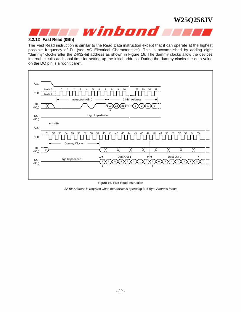
W25Q256JV
- 39 -
8.2.12 Fast Read (0Bh)
The Fast Read instruction is similar to the Read Data instruction except that it can operate at the highest possible frequency of FR (see AC Electrical Characteristics). This is accomplished by adding eight “dummy” clocks after the 24/32-bit address as shown in Figure 16. The dummy clocks allow the devices internal circuits additional time for setting up the initial address. During the dummy clocks the data value on the DO pin is a “don’t care”.
/CS
CLK
DI
(IO0)
DO
(IO1)
Mode 0
Mode 3 0 1 2 3 4 5 6 7
Instruction (0Bh)
High Impedance
8 9 10 28 29 30 31
24-Bit Address
23 22 21 3 2 1 0
Data Out 1
*
/CS
CLK
DI
(IO0)
DO
(IO1)
32 33 34 35 36 37 38 39
Dummy Clocks
High Impedance
40 41 42 44 45 46 47 48 49 50 51 52 53 54 55
7 6 5 4 3 2 1 0 7
Data Out 2
*
7 6 5 4 3 2 1 0
*
4331
0
= MSB*
Figure 16. Fast Read Instruction
32-Bit Address is required when the device is operating in 4-Byte Address Mode
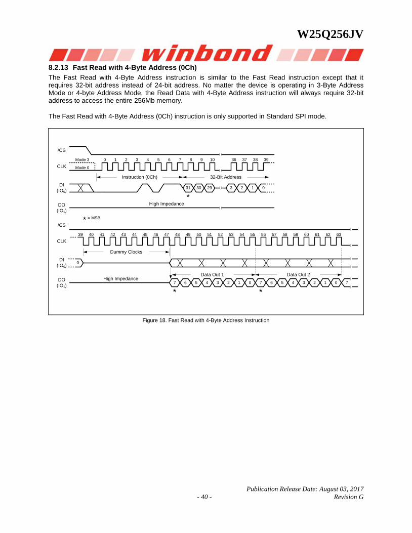
W25Q256JV
Publication Release Date: August 03, 2017
- 40 - Revision G
8.2.13 Fast Read with 4-Byte Address (0Ch)
The Fast Read with 4-Byte Address instruction is similar to the Fast Read instruction except that it requires 32-bit address instead of 24-bit address. No matter the device is operating in 3-Byte Address Mode or 4-byte Address Mode, the Read Data with 4-Byte Address instruction will always require 32-bit address to access the entire 256Mb memory.
The Fast Read with 4-Byte Address (0Ch) instruction is only supported in Standard SPI mode.
/CS
CLK
DI
(IO0)
DO
(IO1)
Mode 0
Mode 3 0 1 2 3 4 5 6 7
Instruction (0Ch)
High Impedance
8 9 10 36 37 38 39
32-Bit Address
31 30 29 3 2 1 0
Data Out 1
*
/CS
CLK
DI
(IO0)
DO
(IO1)
57 58 59 60 61 62 6339
Dummy Clocks
High Impedance
40 41 42 44 45 46 47 48 49 50 51 52 53 54 55
7 6 5 4 3 2 1 0 7
Data Out 2
*
7 6 5 4 3 2 1 0
*
43 56
0
= MSB*
Figure 18. Fast Read with 4-Byte Address Instruction
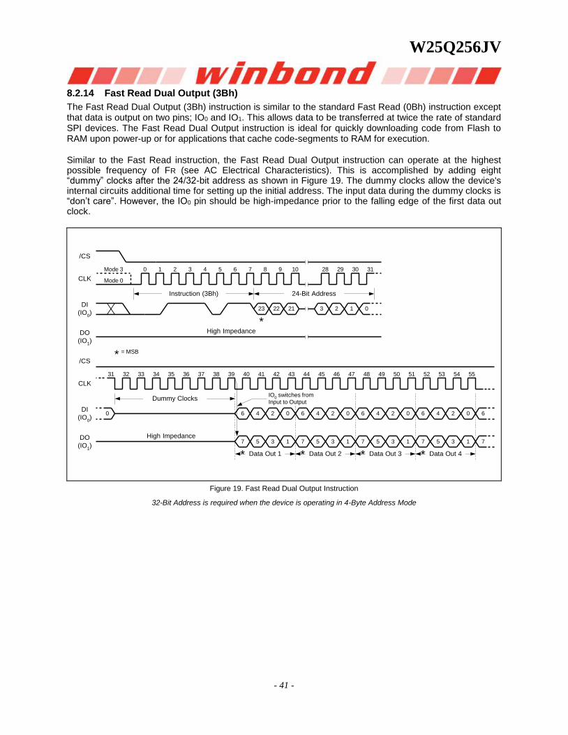
W25Q256JV
- 41 -
8.2.14 Fast Read Dual Output (3Bh)
The Fast Read Dual Output (3Bh) instruction is similar to the standard Fast Read (0Bh) instruction except that data is output on two pins; IO0 and IO1. This allows data to be transferred at twice the rate of standard SPI devices. The Fast Read Dual Output instruction is ideal for quickly downloading code from Flash to RAM upon power-up or for applications that cache code-segments to RAM for execution.
Similar to the Fast Read instruction, the Fast Read Dual Output instruction can operate at the highest possible frequency of FR (see AC Electrical Characteristics). This is accomplished by adding eight “dummy” clocks after the 24/32-bit address as shown in Figure 19. The dummy clocks allow the device's internal circuits additional time for setting up the initial address. The input data during the dummy clocks is “don’t care”. However, the IO0 pin should be high-impedance prior to the falling edge of the first data out clock.
/CS
CLK
DI
(IO0)
DO
(IO1)
Mode 0
Mode 3 0 1 2 3 4 5 6 7
Instruction (3Bh)
High Impedance
8 9 10 28 29 30
32 33 34 35 36 37 38 39
6 4 2 0
24-Bit Address
23 22 21 3 2 1 0
*
*
31
31
/CS
CLK
DI
(IO0)
DO
(IO1)
Dummy Clocks
0
40 41 42 43 44 45 46 47 48 49 50 51 52 53 54 55
7 5 3 1High Impedance
6 4 2 0
7 5 3 1
6 4 2 0
7 5 3 1
6 4 2 0
7 5 3 1
IO0 switches from
Input to Output
6
7
Data Out 1 * Data Out 2 * Data Out 3 * Data Out 4
= MSB*
Figure 19. Fast Read Dual Output Instruction
32-Bit Address is required when the device is operating in 4-Byte Address Mode
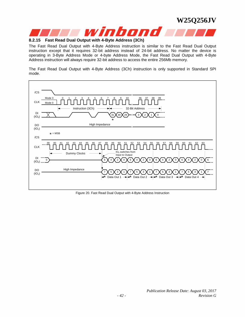
W25Q256JV
Publication Release Date: August 03, 2017
- 42 - Revision G
8.2.15 Fast Read Dual Output with 4-Byte Address (3Ch)
The Fast Read Dual Output with 4-Byte Address instruction is similar to the Fast Read Dual Output instruction except that it requires 32-bit address instead of 24-bit address. No matter the device is operating in 3-Byte Address Mode or 4-byte Address Mode, the Fast Read Dual Output with 4-Byte Address instruction will always require 32-bit address to access the entire 256Mb memory.
The Fast Read Dual Output with 4-Byte Address (3Ch) instruction is only supported in Standard SPI mode.
/CS
CLK
DI
(IO0)
DO
(IO1)
Mode 0
Mode 3 0 1 2 3 4 5 6 7
Instruction (3Ch)
High Impedance
8 9 10 36 37 38
57 58 59 60 61 62 6339
6 4 2 0
32-Bit Address
31 30 29 3 2 1 0
*
*
39
56
/CS
CLK
DI
(IO0)
DO
(IO1)
Dummy Clocks
0
40 41 42 43 44 45 46 47 48 49 50 51 52 53 54 55
7 5 3 1High Impedance
6 4 2 0
7 5 3 1
6 4 2 0
7 5 3 1
6 4 2 0
7 5 3 1
IO0 switches from
Input to Output
6
7
Data Out 1 * Data Out 2 * Data Out 3 * Data Out 4
= MSB*
Figure 20. Fast Read Dual Output with 4-Byte Address Instruction
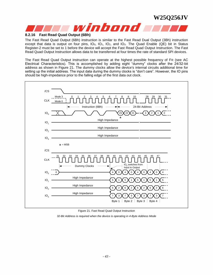
W25Q256JV
- 43 -
8.2.16 Fast Read Quad Output (6Bh)
The Fast Read Quad Output (6Bh) instruction is similar to the Fast Read Dual Output (3Bh) instruction except that data is output on four pins, IO0, IO1, IO2, and IO3. The Quad Enable (QE) bit in Status Register-2 must be set to 1 before the device will accept the Fast Read Quad Output Instruction. The Fast Read Quad Output Instruction allows data to be transferred at four times the rate of standard SPI devices.
The Fast Read Quad Output instruction can operate at the highest possible frequency of FR (see AC Electrical Characteristics). This is accomplished by adding eight “dummy” clocks after the 24/32-bit address as shown in Figure 21. The dummy clocks allow the device's internal circuits additional time for setting up the initial address. The input data during the dummy clocks is “don’t care”. However, the IO pins should be high-impedance prior to the falling edge of the first data out clock.
/CS
CLK Mode 0
Mode 3 0 1 2 3 4 5 6 7
Instruction (6Bh)
High Impedance
8 9 10 28 29 30
32 33 34 35 36 37 38 39
4 0
24-Bit Address
23 22 21 3 2 1 0
*
31
31
/CS
CLK
Dummy Clocks
0
40 41 42 43 44 45 46 47
5 1High Impedance
4
5
Byte 1
High Impedance
High Impedance
6 2
7 3High Impedance
6
7
High Impedance
4 0
5 1
6 2
7 3
4 0
5 1
6 2
7 3
4 0
5 1
6 2
7 3
Byte 2 Byte 3 Byte 4
IO0 switches from
Input to Output
IO0
IO1
IO2
IO3
IO0
IO1
IO2
IO3
= MSB*
Figure 21. Fast Read Quad Output Instruction
32-Bit Address is required when the device is operating in 4-Byte Address Mode
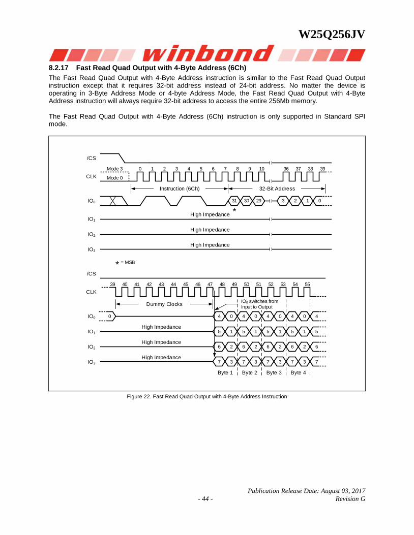
W25Q256JV
Publication Release Date: August 03, 2017
- 44 - Revision G
8.2.17 Fast Read Quad Output with 4-Byte Address (6Ch)
The Fast Read Quad Output with 4-Byte Address instruction is similar to the Fast Read Quad Output instruction except that it requires 32-bit address instead of 24-bit address. No matter the device is operating in 3-Byte Address Mode or 4-byte Address Mode, the Fast Read Quad Output with 4-Byte Address instruction will always require 32-bit address to access the entire 256Mb memory.
The Fast Read Quad Output with 4-Byte Address (6Ch) instruction is only supported in Standard SPI mode.
/CS
CLK Mode 0
Mode 3 0 1 2 3 4 5 6 7
Instruction (6Ch)
High Impedance
8 9 10 36 37 38
49 50 51 52 53 54 5539
4 0
32-Bit Address
31 30 29 3 2 1 0
*
39
48
/CS
CLK
Dummy Clocks
0
40 41 42 43 44 45 46 47
5 1High Impedance
4
5
Byte 1
High Impedance
High Impedance
6 2
7 3High Impedance
6
7
High Impedance
4 0
5 1
6 2
7 3
4 0
5 1
6 2
7 3
4 0
5 1
6 2
7 3
Byte 2 Byte 3 Byte 4
IO0 switches fromInput to Output
IO0
IO1
IO2
IO3
IO0
IO1
IO2
IO3
= MSB*
Figure 22. Fast Read Quad Output with 4-Byte Address Instruction
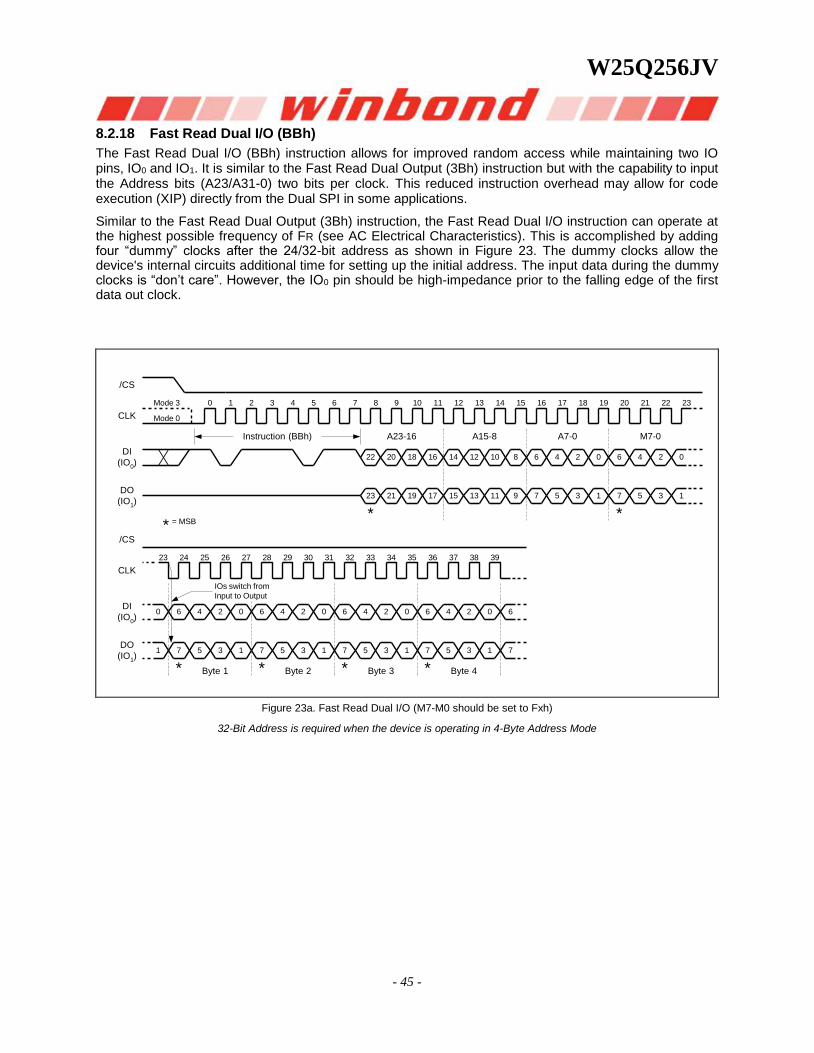
W25Q256JV
- 45 -
8.2.18 Fast Read Dual I/O (BBh)
The Fast Read Dual I/O (BBh) instruction allows for improved random access while maintaining two IO pins, IO0 and IO1. It is similar to the Fast Read Dual Output (3Bh) instruction but with the capability to input the Address bits (A23/A31-0) two bits per clock. This reduced instruction overhead may allow for code execution (XIP) directly from the Dual SPI in some applications.
Similar to the Fast Read Dual Output (3Bh) instruction, the Fast Read Dual I/O instruction can operate at the highest possible frequency of FR (see AC Electrical Characteristics). This is accomplished by adding four “dummy” clocks after the 24/32-bit address as shown in Figure 23. The dummy clocks allow the device's internal circuits additional time for setting up the initial address. The input data during the dummy clocks is “don’t care”. However, the IO0 pin should be high-impedance prior to the falling edge of the first data out clock.
/CS
CLK
DI
(IO0)
DO
(IO1)
Mode 0
Mode 3 0 1 2 3 4 5 6 7
Instruction (BBh)
8 9 10 12 13 14
24 25 26 27 28 29 30 31
6 4 2 0
*
*
23
/CS
CLK
DI
(IO0)
DO
(IO1)
0
32 33 34 35 36 37 38 39
7 5 3 1
*
6 4 2 0
7 5 3 1
6 4 2 0
7 5 3 1
6 4 2 0
7 5 3 1
* *
IOs switch from
Input to Output
6
7
22 20 18 16
23 21 19 17
14 12 10 8
15 13 11 9
6 4 2 0
7 5 3 1
6 4 2 0
7 5 3 1
11 15 16 17 18 20 21 2219 23
1
A23-16 A15-8 A7-0 M7-0
Byte 1 Byte 2 Byte 3 Byte 4
= MSB**
Figure 23a. Fast Read Dual I/O (M7-M0 should be set to Fxh)
32-Bit Address is required when the device is operating in 4-Byte Address Mode
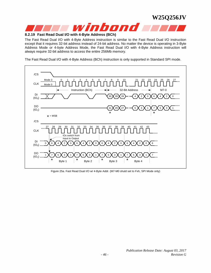
W25Q256JV
Publication Release Date: August 03, 2017
- 46 - Revision G
8.2.19 Fast Read Dual I/O with 4-Byte Address (BCh)
The Fast Read Dual I/O with 4-Byte Address instruction is similar to the Fast Read Dual I/O instruction except that it requires 32-bit address instead of 24-bit address. No matter the device is operating in 3-Byte Address Mode or 4-byte Address Mode, the Fast Read Dual I/O with 4-Byte Address instruction will always require 32-bit address to access the entire 256Mb memory.
The Fast Read Dual I/O with 4-Byte Address (BCh) instruction is only supported in Standard SPI mode.
/CS
CLK
DI
(IO0)
DO
(IO1)
Mode 0
Mode 3 0 1 2 3 4 5 6 7
Instruction (BCh)
8 9 10
41 42 4327 28 29 30 31
6 4 2 0
*
*
40
/CS
CLK
DI
(IO0)
DO
(IO1)
0
32 33 34 35 36 37 38 39
7 5 3 1
*
6 4 2 0
7 5 3 1
6 4 2 0
7 5 3 1
6 4 2 0
7 5 3 1
* *
IOs switch from
Input to Output
6
7
30 28 26
31 29 27
4 2 0
5 3 1
6 4 2 0
7 5 3 1
21 22 24 25 2623 27
1
M7-0
Byte 1 Byte 2 Byte 3 Byte 4
= MSB**
32-Bit Address
Figure 25a. Fast Read Dual I/O w/ 4-Byte Addr. (M7-M0 shuld set to Fxh, SPI Mode only)
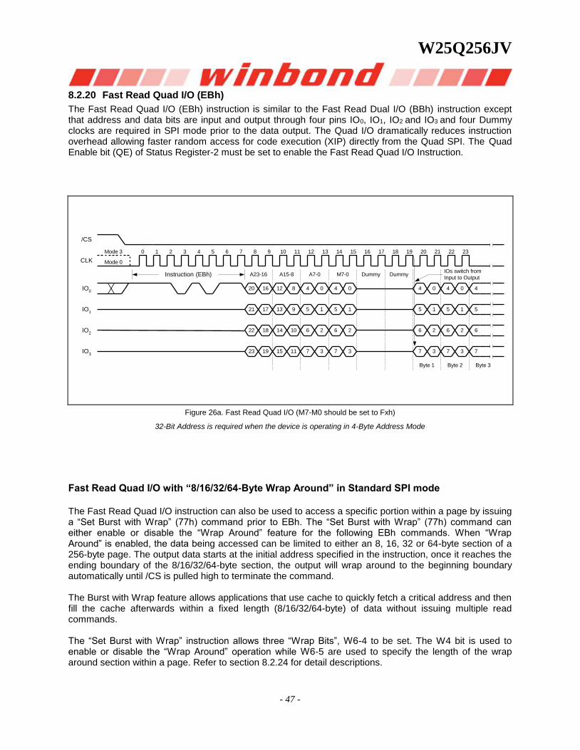
W25Q256JV
- 47 -
8.2.20 Fast Read Quad I/O (EBh)
The Fast Read Quad I/O (EBh) instruction is similar to the Fast Read Dual I/O (BBh) instruction except that address and data bits are input and output through four pins IO0, IO1, IO2 and IO3 and four Dummy clocks are required in SPI mode prior to the data output. The Quad I/O dramatically reduces instruction overhead allowing faster random access for code execution (XIP) directly from the Quad SPI. The Quad Enable bit (QE) of Status Register-2 must be set to enable the Fast Read Quad I/O Instruction.
Figure 26a. Fast Read Quad I/O (M7-M0 should be set to Fxh)
32-Bit Address is required when the device is operating in 4-Byte Address Mode
Fast Read Quad I/O with “8/16/32/64-Byte Wrap Around” in Standard SPI mode
The Fast Read Quad I/O instruction can also be used to access a specific portion within a page by issuing a “Set Burst with Wrap” (77h) command prior to EBh. The “Set Burst with Wrap” (77h) command can either enable or disable the “Wrap Around” feature for the following EBh commands. When “Wrap Around” is enabled, the data being accessed can be limited to either an 8, 16, 32 or 64-byte section of a 256-byte page. The output data starts at the initial address specified in the instruction, once it reaches the ending boundary of the 8/16/32/64-byte section, the output will wrap around to the beginning boundary automatically until /CS is pulled high to terminate the command. The Burst with Wrap feature allows applications that use cache to quickly fetch a critical address and then fill the cache afterwards within a fixed length (8/16/32/64-byte) of data without issuing multiple read commands. The “Set Burst with Wrap” instruction allows three “Wrap Bits”, W6-4 to be set. The W4 bit is used to enable or disable the “Wrap Around” operation while W6-5 are used to specify the length of the wrap around section within a page. Refer to section 8.2.24 for detail descriptions.
M7-0
/CS
CLK Mode 0
Mode 3 0 1
IO0
IO1
IO2
IO3
2 3 4 5
20 16 12 8
21 17
22 18
23 19
13 9
14 10
15 11
A23-16
6 7 8 9
4 0
5 1
6 2
7 3
A15-8 A7-0
Byte 1 Byte 2
4 0
5 1
6 2
7 3
4 0
5 1
6 2
7 3
4 0
5 1
6 2
7 3
10 11 12 13 14
4
5
6
7
IOs switch from
Input to Output
Byte 3
15 16 17 18 19 20 21 22 23
Dummy DummyInstruction (EBh)
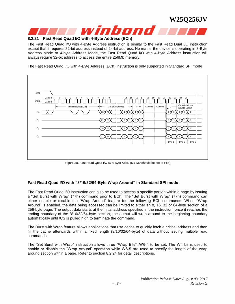
W25Q256JV
Publication Release Date: August 03, 2017
- 48 - Revision G
8.2.21 Fast Read Quad I/O with 4-Byte Address (ECh)
The Fast Read Quad I/O with 4-Byte Address instruction is similar to the Fast Read Dual I/O instruction except that it requires 32-bit address instead of 24-bit address. No matter the device is operating in 3-Byte Address Mode or 4-byte Address Mode, the Fast Read Quad I/O with 4-Byte Address instruction will always require 32-bit address to access the entire 256Mb memory.
The Fast Read Quad I/O with 4-Byte Address (ECh) instruction is only supported in Standard SPI mode.
Figure 28. Fast Read Quad I/O w/ 4-Byte Addr. (M7-M0 should be set to Fxh)
Fast Read Quad I/O with “8/16/32/64-Byte Wrap Around” in Standard SPI mode
The Fast Read Quad I/O instruction can also be used to access a specific portion within a page by issuing a “Set Burst with Wrap” (77h) command prior to ECh. The “Set Burst with Wrap” (77h) command can either enable or disable the “Wrap Around” feature for the following ECh commands. When “Wrap Around” is enabled, the data being accessed can be limited to either an 8, 16, 32 or 64-byte section of a 256-byte page. The output data starts at the initial address specified in the instruction, once it reaches the ending boundary of the 8/16/32/64-byte section, the output will wrap around to the beginning boundary automatically until /CS is pulled high to terminate the command. The Burst with Wrap feature allows applications that use cache to quickly fetch a critical address and then fill the cache afterwards within a fixed length (8/16/32/64-byte) of data without issuing multiple read commands. The “Set Burst with Wrap” instruction allows three “Wrap Bits”, W6-4 to be set. The W4 bit is used to enable or disable the “Wrap Around” operation while W6-5 are used to specify the length of the wrap around section within a page. Refer to section 8.2.24 for detail descriptions.
M7-0
/CS
CLK Mode 0
Mode 3 0 1
IO0
IO1
IO2
IO3
2 3 4 5
28 24
29 25
30 26
31 27
6 7 8 9
4 0
5 1
6 2
7 3
Byte 1 Byte 2
4 0
5 1
6 2
7 3
4 0
5 1
6 2
7 3
4 0
5 1
6 2
7 3
14 15 16
4
5
6
7
IOs switch from
Input to Output
Byte 3
17 18 19 20 21 22 23 24 25
Dummy DummyInstruction (ECh) 32-Bit Address
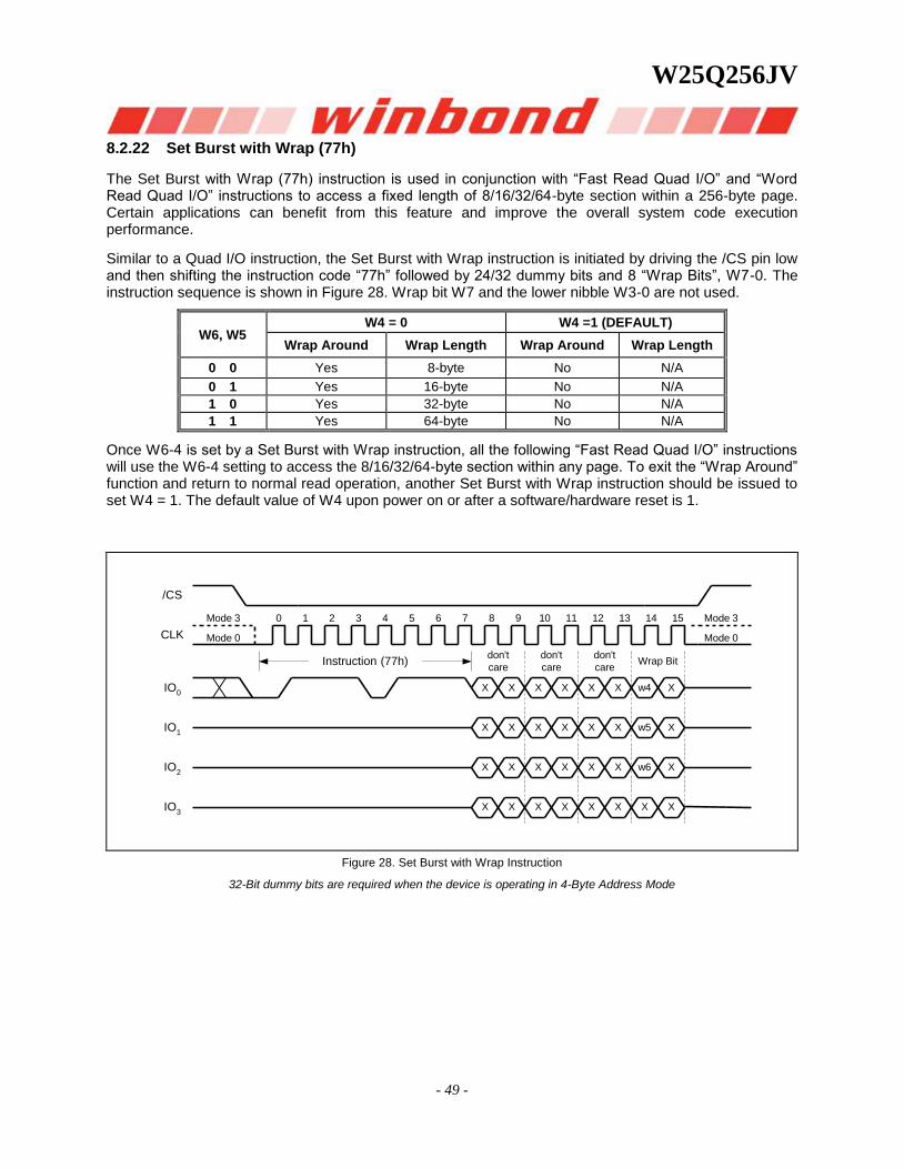
W25Q256JV
- 49 -
8.2.22 Set Burst with Wrap (77h)
The Set Burst with Wrap (77h) instruction is used in conjunction with “Fast Read Quad I/O” and “Word Read Quad I/O” instructions to access a fixed length of 8/16/32/64-byte section within a 256-byte page. Certain applications can benefit from this feature and improve the overall system code execution performance.
Similar to a Quad I/O instruction, the Set Burst with Wrap instruction is initiated by driving the /CS pin low and then shifting the instruction code “77h” followed by 24/32 dummy bits and 8 “Wrap Bits”, W7-0. The instruction sequence is shown in Figure 28. Wrap bit W7 and the lower nibble W3-0 are not used.
W6, W5 W4 = 0 W4 =1 (DEFAULT)
Wrap Around Wrap Length Wrap Around Wrap Length
0 0 Yes 8-byte No N/A
0 1 Yes 16-byte No N/A
1 0 Yes 32-byte No N/A
1 1 Yes 64-byte No N/A
Once W6-4 is set by a Set Burst with Wrap instruction, all the following “Fast Read Quad I/O” instructions will use the W6-4 setting to access the 8/16/32/64-byte section within any page. To exit the “Wrap Around” function and return to normal read operation, another Set Burst with Wrap instruction should be issued to set W4 = 1. The default value of W4 upon power on or after a software/hardware reset is 1.
Wrap Bit
/CS
CLK Mode 0
Mode 3 0 1
IO0
IO1
IO2
IO3
2 3 4 5
X X
X X
X X
X X
don't
care
6 7 8 9
don't
care
don't
care
10 11 12 13 14 15
Instruction (77h)
Mode 0
Mode 3
X X
X X
X X
X X
X X
X X
X X
X X
w4 X
w5 X
w6 X
X X
Figure 28. Set Burst with Wrap Instruction
32-Bit dummy bits are required when the device is operating in 4-Byte Address Mode
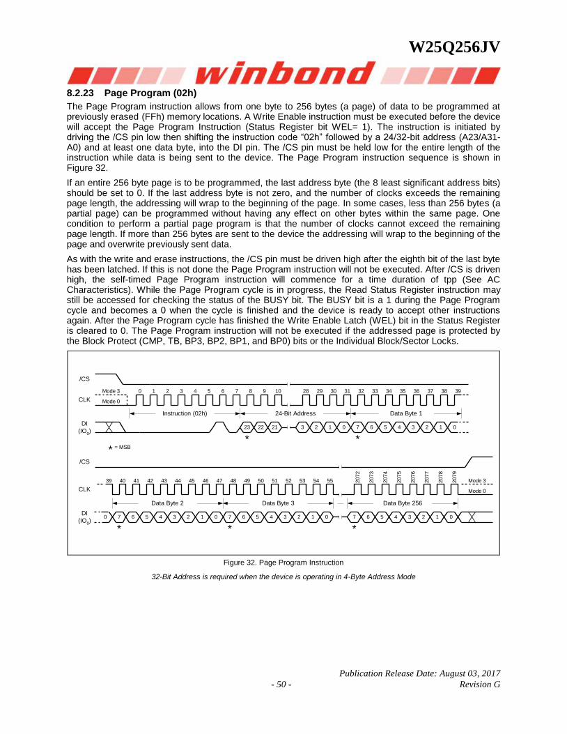
W25Q256JV
Publication Release Date: August 03, 2017
- 50 - Revision G
8.2.23 Page Program (02h)
The Page Program instruction allows from one byte to 256 bytes (a page) of data to be programmed at previously erased (FFh) memory locations. A Write Enable instruction must be executed before the device will accept the Page Program Instruction (Status Register bit WEL= 1). The instruction is initiated by driving the /CS pin low then shifting the instruction code “02h” followed by a 24/32-bit address (A23/A31-A0) and at least one data byte, into the DI pin. The /CS pin must be held low for the entire length of the instruction while data is being sent to the device. The Page Program instruction sequence is shown in Figure 32.
If an entire 256 byte page is to be programmed, the last address byte (the 8 least significant address bits) should be set to 0. If the last address byte is not zero, and the number of clocks exceeds the remaining page length, the addressing will wrap to the beginning of the page. In some cases, less than 256 bytes (a partial page) can be programmed without having any effect on other bytes within the same page. One condition to perform a partial page program is that the number of clocks cannot exceed the remaining page length. If more than 256 bytes are sent to the device the addressing will wrap to the beginning of the page and overwrite previously sent data.
As with the write and erase instructions, the /CS pin must be driven high after the eighth bit of the last byte has been latched. If this is not done the Page Program instruction will not be executed. After /CS is driven high, the self-timed Page Program instruction will commence for a time duration of tpp (See AC Characteristics). While the Page Program cycle is in progress, the Read Status Register instruction may still be accessed for checking the status of the BUSY bit. The BUSY bit is a 1 during the Page Program cycle and becomes a 0 when the cycle is finished and the device is ready to accept other instructions again. After the Page Program cycle has finished the Write Enable Latch (WEL) bit in the Status Register is cleared to 0. The Page Program instruction will not be executed if the addressed page is protected by the Block Protect (CMP, TB, BP3, BP2, BP1, and BP0) bits or the Individual Block/Sector Locks.
/CS
CLK
DI
(IO0)
Mode 0
Mode 3 0 1 2 3 4 5 6 7
Instruction (02h)
8 9 10 28 29 30 39
24-Bit Address
23 22 21 3 2 1
*
/CS
CLK
DI
(IO0)
40 41 42 43 44 45 46 47
Data Byte 2
48 49 50 52 53 54 55 2072
7 6 5 4 3 2 1 0
5139
0
31
0
32 33 34 35 36 37 38
Data Byte 1
7 6 5 4 3 2 1
*
Mode 0
Mode 3
Data Byte 3
2073
2074
2075
2076
2077
2078
2079
0
Data Byte 256
*
7 6 5 4 3 2 1 0
*
7 6 5 4 3 2 1 0
*
= MSB*
Figure 32. Page Program Instruction
32-Bit Address is required when the device is operating in 4-Byte Address Mode
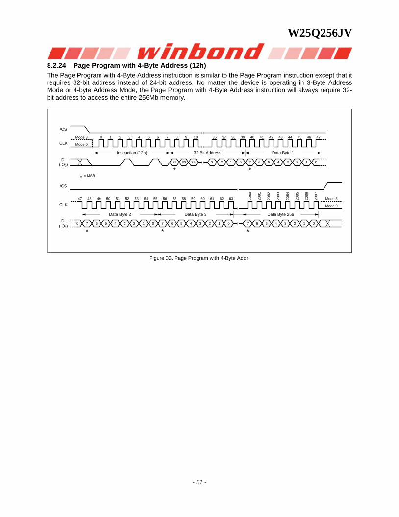
W25Q256JV
- 51 -
8.2.24 Page Program with 4-Byte Address (12h)
The Page Program with 4-Byte Address instruction is similar to the Page Program instruction except that it requires 32-bit address instead of 24-bit address. No matter the device is operating in 3-Byte Address Mode or 4-byte Address Mode, the Page Program with 4-Byte Address instruction will always require 32-bit address to access the entire 256Mb memory.
/CS
CLK
DI
(IO0)
Mode 0
Mode 3 0 1 2 3 4 5 6 7
Instruction (12h)
8 9 10 36 37 38 47
32-Bit Address
31 30 29 3 2 1
*
/CS
CLK
DI
(IO0)
48 49 50 51 52 53 54 55
Data Byte 2
56 57 58 60 61 62 63 20
80
7 6 5 4 3 2 1 0
5947
0
39
0
40 41 42 43 44 45 46
Data Byte 1
7 6 5 4 3 2 1
*
Mode 0
Mode 3
Data Byte 3
20
81
20
82
20
83
20
84
20
85
20
86
20
87
0
Data Byte 256
*
7 6 5 4 3 2 1 0
*
7 6 5 4 3 2 1 0
*
= MSB*
Figure 33. Page Program with 4-Byte Addr.
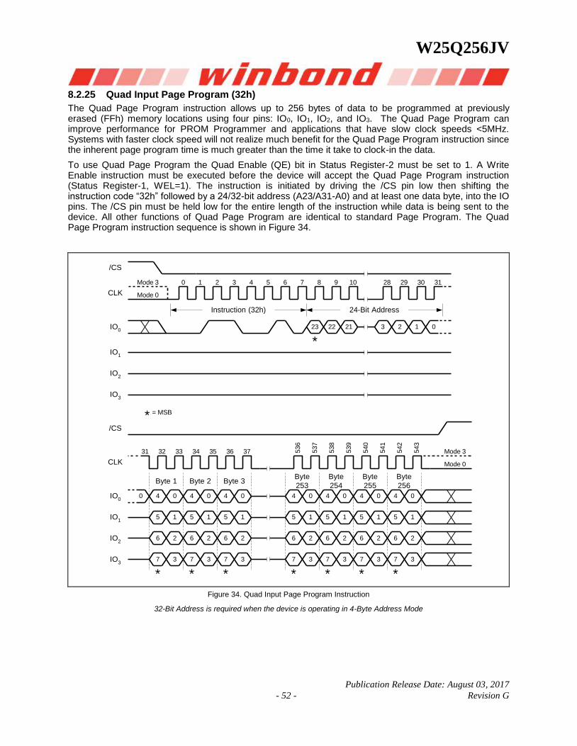
W25Q256JV
Publication Release Date: August 03, 2017
- 52 - Revision G
8.2.25 Quad Input Page Program (32h)
The Quad Page Program instruction allows up to 256 bytes of data to be programmed at previously erased (FFh) memory locations using four pins: IO0, IO1, IO2, and IO3. The Quad Page Program can improve performance for PROM Programmer and applications that have slow clock speeds <5MHz. Systems with faster clock speed will not realize much benefit for the Quad Page Program instruction since the inherent page program time is much greater than the time it take to clock-in the data.
To use Quad Page Program the Quad Enable (QE) bit in Status Register-2 must be set to 1. A Write Enable instruction must be executed before the device will accept the Quad Page Program instruction (Status Register-1, WEL=1). The instruction is initiated by driving the /CS pin low then shifting the instruction code “32h” followed by a 24/32-bit address (A23/A31-A0) and at least one data byte, into the IO pins. The /CS pin must be held low for the entire length of the instruction while data is being sent to the device. All other functions of Quad Page Program are identical to standard Page Program. The Quad Page Program instruction sequence is shown in Figure 34.
/CS
CLK Mode 0
Mode 3 0 1 2 3 4 5 6 7
Instruction (32h)
8 9 10 28 29 30
32 33 34 35 36 37
4 0
24-Bit Address
23 22 21 3 2 1 0
*
31
31
/CS
CLK
5 1
Byte 1
6 2
7 3
4 0
5 1
6 2
7 3
4 0
5 1
6 2
7 3
4 0
5 1
6 2
7 3
Byte 2 Byte 3Byte
256
0 4 0
5 1
6 2
7 3
4 0
5 1
6 2
7 3
4 0
5 1
6 2
7 3
536
537
538
539
540
541
542
543
Mode 0
Mode 3
Byte
253
Byte
254
Byte
255
IO0
IO1
IO2
IO3
IO0
IO1
IO2
IO3
* * * * * * *
= MSB*
Figure 34. Quad Input Page Program Instruction
32-Bit Address is required when the device is operating in 4-Byte Address Mode
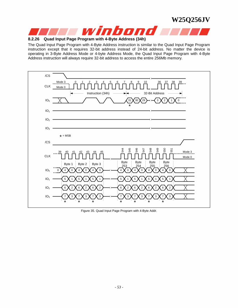
W25Q256JV
- 53 -
8.2.26 Quad Input Page Program with 4-Byte Address (34h)
The Quad Input Page Program with 4-Byte Address instruction is similar to the Quad Input Page Program instruction except that it requires 32-bit address instead of 24-bit address. No matter the device is operating in 3-Byte Address Mode or 4-byte Address Mode, the Quad Input Page Program with 4-Byte Address instruction will always require 32-bit address to access the entire 256Mb memory.
/CS
CLK Mode 0
Mode 3 0 1 2 3 4 5 6 7
Instruction (34h)
8 9 10 36 37 38
40 41 42 43 44 45
4 0
32-Bit Address
31 30 29 3 2 1 0
*
39
39
/CS
CLK
5 1
Byte 1
6 2
7 3
4 0
5 1
6 2
7 3
4 0
5 1
6 2
7 3
4 0
5 1
6 2
7 3
Byte 2 Byte 3Byte
256
0 4 0
5 1
6 2
7 3
4 0
5 1
6 2
7 3
4 0
5 1
6 2
7 3
54
4
54
5
54
6
54
7
54
8
54
9
55
0
55
1
Mode 0
Mode 3
Byte
253
Byte
254
Byte
255
IO0
IO1
IO2
IO3
IO0
IO1
IO2
IO3
* * * * * * *
= MSB*
Figure 35. Quad Input Page Program with 4-Byte Addr.
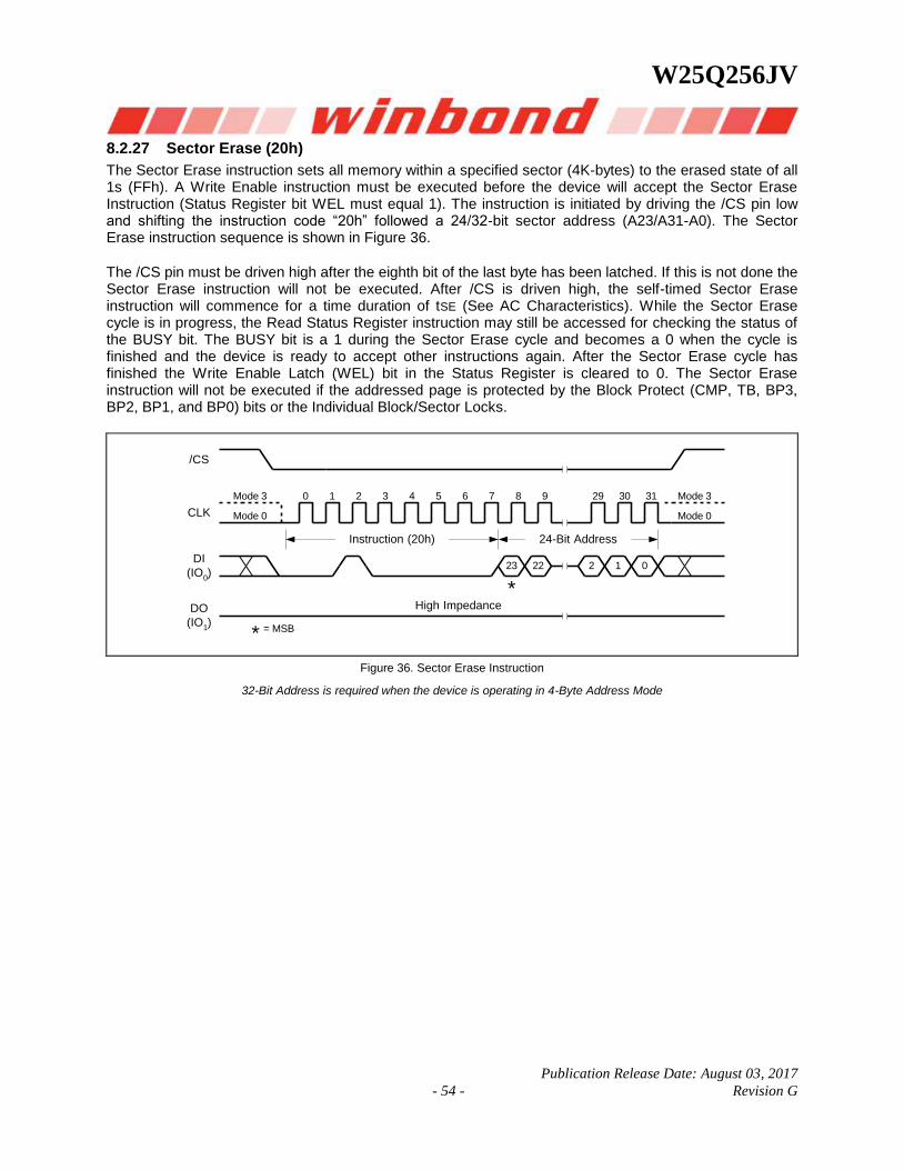
W25Q256JV
Publication Release Date: August 03, 2017
- 54 - Revision G
8.2.27 Sector Erase (20h)
The Sector Erase instruction sets all memory within a specified sector (4K-bytes) to the erased state of all 1s (FFh). A Write Enable instruction must be executed before the device will accept the Sector Erase Instruction (Status Register bit WEL must equal 1). The instruction is initiated by driving the /CS pin low and shifting the instruction code “20h” followed a 24/32-bit sector address (A23/A31-A0). The Sector Erase instruction sequence is shown in Figure 36.
The /CS pin must be driven high after the eighth bit of the last byte has been latched. If this is not done the Sector Erase instruction will not be executed. After /CS is driven high, the self-timed Sector Erase instruction will commence for a time duration of tSE (See AC Characteristics). While the Sector Erase cycle is in progress, the Read Status Register instruction may still be accessed for checking the status of the BUSY bit. The BUSY bit is a 1 during the Sector Erase cycle and becomes a 0 when the cycle is finished and the device is ready to accept other instructions again. After the Sector Erase cycle has finished the Write Enable Latch (WEL) bit in the Status Register is cleared to 0. The Sector Erase instruction will not be executed if the addressed page is protected by the Block Protect (CMP, TB, BP3, BP2, BP1, and BP0) bits or the Individual Block/Sector Locks.
/CS
CLK
DI
(IO0)
DO
(IO1)
Mode 0
Mode 3 0 1 2 3 4 5 6 7
Instruction (20h)
High Impedance
8 9 29 30 31
24-Bit Address
23 22 2 1 0
*
Mode 0
Mode 3
= MSB*
Figure 36. Sector Erase Instruction
32-Bit Address is required when the device is operating in 4-Byte Address Mode
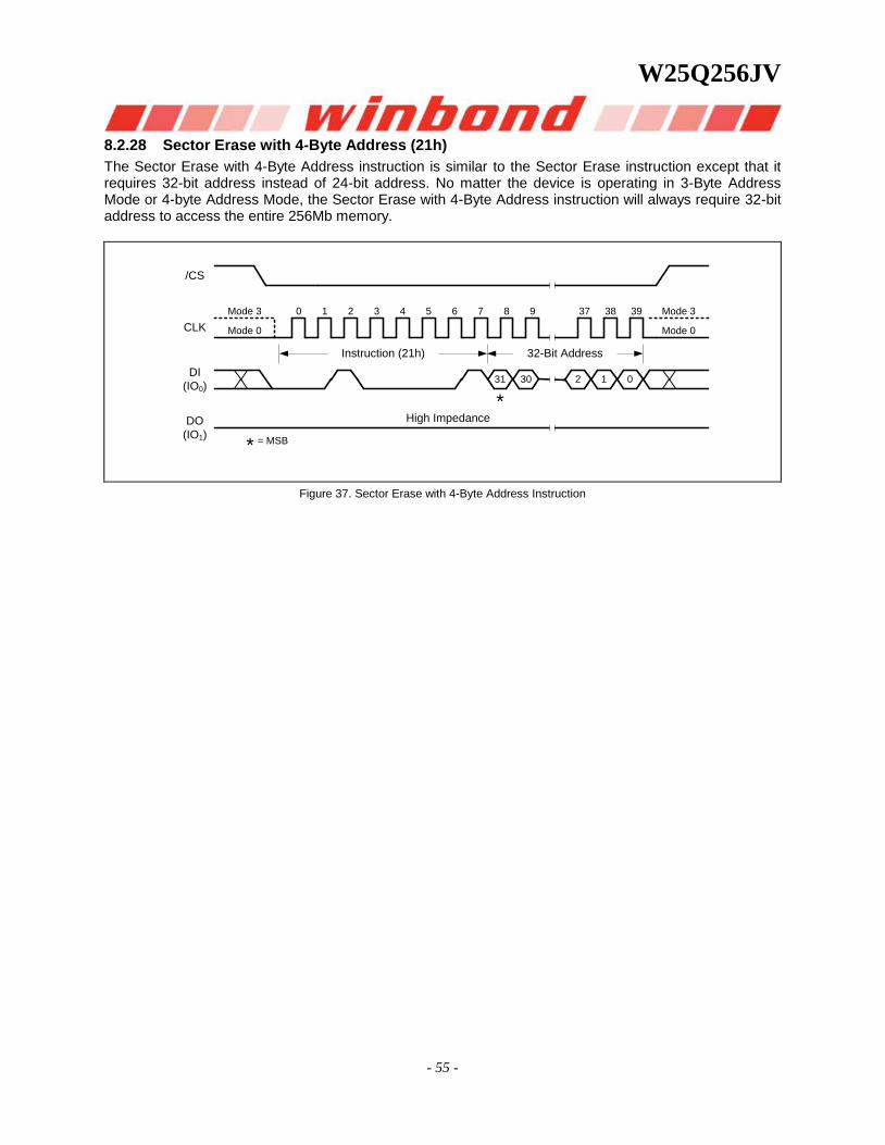
W25Q256JV
- 55 -
8.2.28 Sector Erase with 4-Byte Address (21h)
The Sector Erase with 4-Byte Address instruction is similar to the Sector Erase instruction except that it requires 32-bit address instead of 24-bit address. No matter the device is operating in 3-Byte Address Mode or 4-byte Address Mode, the Sector Erase with 4-Byte Address instruction will always require 32-bit address to access the entire 256Mb memory.
/CS
CLK
DI
(IO0)
DO
(IO1)
Mode 0
Mode 3 0 1 2 3 4 5 6 7
Instruction (21h)
High Impedance
8 9 37 38 39
32-Bit Address
31 30 2 1 0
*
Mode 0
Mode 3
= MSB*
Figure 37. Sector Erase with 4-Byte Address Instruction
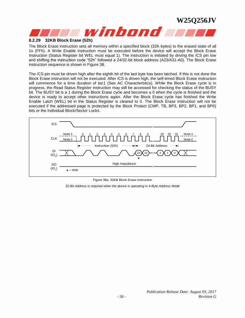
W25Q256JV
Publication Release Date: August 03, 2017
- 56 - Revision G
8.2.29 32KB Block Erase (52h)
The Block Erase instruction sets all memory within a specified block (32K-bytes) to the erased state of all 1s (FFh). A Write Enable instruction must be executed before the device will accept the Block Erase Instruction (Status Register bit WEL must equal 1). The instruction is initiated by driving the /CS pin low and shifting the instruction code “52h” followed a 24/32-bit block address (A23/A31-A0). The Block Erase instruction sequence is shown in Figure 38.
The /CS pin must be driven high after the eighth bit of the last byte has been latched. If this is not done the Block Erase instruction will not be executed. After /CS is driven high, the self-timed Block Erase instruction will commence for a time duration of tBE1 (See AC Characteristics). While the Block Erase cycle is in progress, the Read Status Register instruction may still be accessed for checking the status of the BUSY bit. The BUSY bit is a 1 during the Block Erase cycle and becomes a 0 when the cycle is finished and the device is ready to accept other instructions again. After the Block Erase cycle has finished the Write Enable Latch (WEL) bit in the Status Register is cleared to 0. The Block Erase instruction will not be executed if the addressed page is protected by the Block Protect (CMP, TB, BP3, BP2, BP1, and BP0) bits or the Individual Block/Sector Locks.
/CS
CLK
DI
(IO0)
DO
(IO1)
Mode 0
Mode 3 0 1 2 3 4 5 6 7
Instruction (52h)
High Impedance
8 9 29 30 31
24-Bit Address
23 22 2 1 0
*
Mode 0
Mode 3
= MSB*
Figure 38a. 32KB Block Erase Instruction
32-Bit Address is required when the device is operating in 4-Byte Address Mode
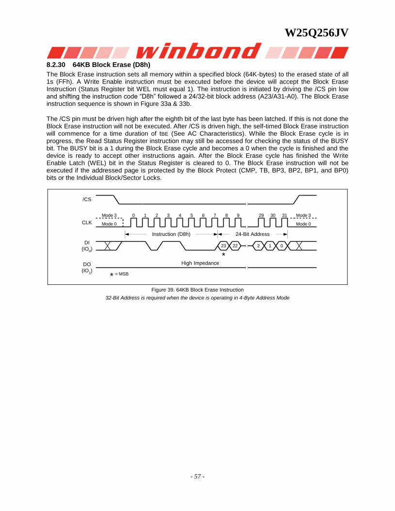
W25Q256JV
- 57 -
8.2.30 64KB Block Erase (D8h)
The Block Erase instruction sets all memory within a specified block (64K-bytes) to the erased state of all 1s (FFh). A Write Enable instruction must be executed before the device will accept the Block Erase Instruction (Status Register bit WEL must equal 1). The instruction is initiated by driving the /CS pin low and shifting the instruction code “D8h” followed a 24/32-bit block address (A23/A31-A0). The Block Erase instruction sequence is shown in Figure 33a & 33b.
The /CS pin must be driven high after the eighth bit of the last byte has been latched. If this is not done the Block Erase instruction will not be executed. After /CS is driven high, the self-timed Block Erase instruction will commence for a time duration of tBE (See AC Characteristics). While the Block Erase cycle is in progress, the Read Status Register instruction may still be accessed for checking the status of the BUSY bit. The BUSY bit is a 1 during the Block Erase cycle and becomes a 0 when the cycle is finished and the device is ready to accept other instructions again. After the Block Erase cycle has finished the Write Enable Latch (WEL) bit in the Status Register is cleared to 0. The Block Erase instruction will not be executed if the addressed page is protected by the Block Protect (CMP, TB, BP3, BP2, BP1, and BP0) bits or the Individual Block/Sector Locks.
/CS
CLK
DI
(IO0)
DO
(IO1)
Mode 0
Mode 3 0 1 2 3 4 5 6 7
Instruction (D8h)
High Impedance
8 9 29 30 31
24-Bit Address
23 22 2 1 0
*
Mode 0
Mode 3
= MSB*
Figure 39. 64KB Block Erase Instruction
32-Bit Address is required when the device is operating in 4-Byte Address Mode
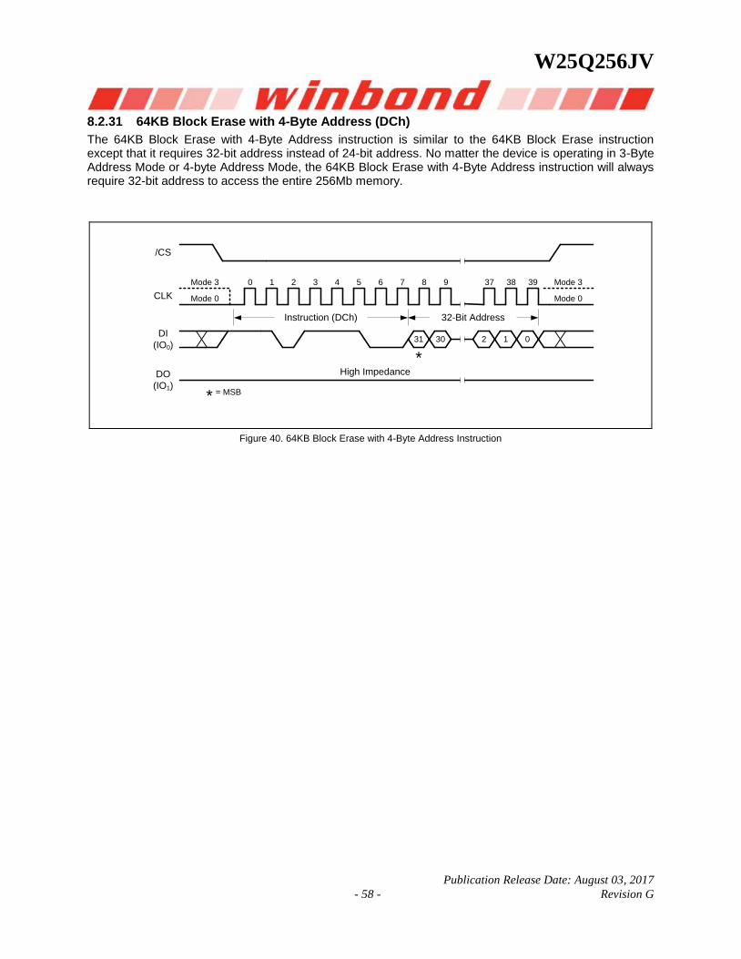
W25Q256JV
Publication Release Date: August 03, 2017
- 58 - Revision G
8.2.31 64KB Block Erase with 4-Byte Address (DCh)
The 64KB Block Erase with 4-Byte Address instruction is similar to the 64KB Block Erase instruction except that it requires 32-bit address instead of 24-bit address. No matter the device is operating in 3-Byte Address Mode or 4-byte Address Mode, the 64KB Block Erase with 4-Byte Address instruction will always require 32-bit address to access the entire 256Mb memory.
/CS
CLK
DI
(IO0)
DO
(IO1)
Mode 0
Mode 3 0 1 2 3 4 5 6 7
Instruction (DCh)
High Impedance
8 9 37 38 39
32-Bit Address
31 30 2 1 0
*
Mode 0
Mode 3
= MSB*
Figure 40. 64KB Block Erase with 4-Byte Address Instruction
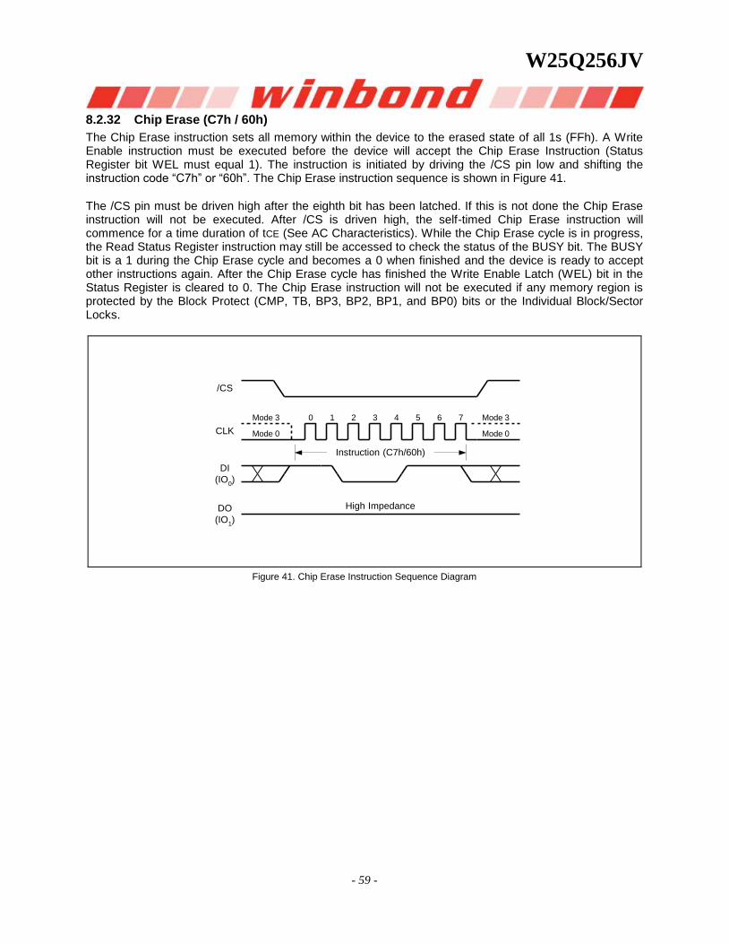
W25Q256JV
- 59 -
8.2.32 Chip Erase (C7h / 60h)
The Chip Erase instruction sets all memory within the device to the erased state of all 1s (FFh). A Write Enable instruction must be executed before the device will accept the Chip Erase Instruction (Status Register bit WEL must equal 1). The instruction is initiated by driving the /CS pin low and shifting the instruction code “C7h” or “60h”. The Chip Erase instruction sequence is shown in Figure 41.
The /CS pin must be driven high after the eighth bit has been latched. If this is not done the Chip Erase instruction will not be executed. After /CS is driven high, the self-timed Chip Erase instruction will commence for a time duration of tCE (See AC Characteristics). While the Chip Erase cycle is in progress, the Read Status Register instruction may still be accessed to check the status of the BUSY bit. The BUSY bit is a 1 during the Chip Erase cycle and becomes a 0 when finished and the device is ready to accept other instructions again. After the Chip Erase cycle has finished the Write Enable Latch (WEL) bit in the Status Register is cleared to 0. The Chip Erase instruction will not be executed if any memory region is protected by the Block Protect (CMP, TB, BP3, BP2, BP1, and BP0) bits or the Individual Block/Sector Locks.
/CS
CLK
DI
(IO0)
DO
(IO1)
Mode 0
Mode 3 0 1 2 3 4 5 6 7
Instruction (C7h/60h)
High Impedance
Mode 0
Mode 3
Figure 41. Chip Erase Instruction Sequence Diagram
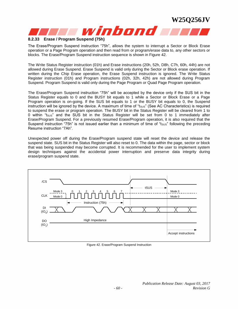
W25Q256JV
Publication Release Date: August 03, 2017
- 60 - Revision G
8.2.33 Erase / Program Suspend (75h)
The Erase/Program Suspend instruction “75h”, allows the system to interrupt a Sector or Block Erase operation or a Page Program operation and then read from or program/erase data to, any other sectors or blocks. The Erase/Program Suspend instruction sequence is shown in Figure 42.
The Write Status Register instruction (01h) and Erase instructions (20h, 52h, D8h, C7h, 60h, 44h) are not allowed during Erase Suspend. Erase Suspend is valid only during the Sector or Block erase operation. If written during the Chip Erase operation, the Erase Suspend instruction is ignored. The Write Status Register instruction (01h) and Program instructions (02h, 32h, 42h) are not allowed during Program Suspend. Program Suspend is valid only during the Page Program or Quad Page Program operation.
The Erase/Program Suspend instruction “75h” will be accepted by the device only if the SUS bit in the Status Register equals to 0 and the BUSY bit equals to 1 while a Sector or Block Erase or a Page Program operation is on-going. If the SUS bit equals to 1 or the BUSY bit equals to 0, the Suspend instruction will be ignored by the device. A maximum of time of “tSUS” (See AC Characteristics) is required to suspend the erase or program operation. The BUSY bit in the Status Register will be cleared from 1 to 0 within “tSUS” and the SUS bit in the Status Register will be set from 0 to 1 immediately after Erase/Program Suspend. For a previously resumed Erase/Program operation, it is also required that the Suspend instruction “75h” is not issued earlier than a minimum of time of “tSUS” following the preceding Resume instruction “7Ah”.
Unexpected power off during the Erase/Program suspend state will reset the device and release the suspend state. SUS bit in the Status Register will also reset to 0. The data within the page, sector or block that was being suspended may become corrupted. It is recommended for the user to implement system design techniques against the accidental power interruption and preserve data integrity during erase/program suspend state.
/CS
CLK
DI
(IO0)
DO
(IO1)
Mode 0
Mode 3 0 1 2 3 4 5 6 7
Instruction (75h)
High Impedance
Mode 0
Mode 3
tSUS
Accept instructions
Figure 42. Erase/Program Suspend Instruction
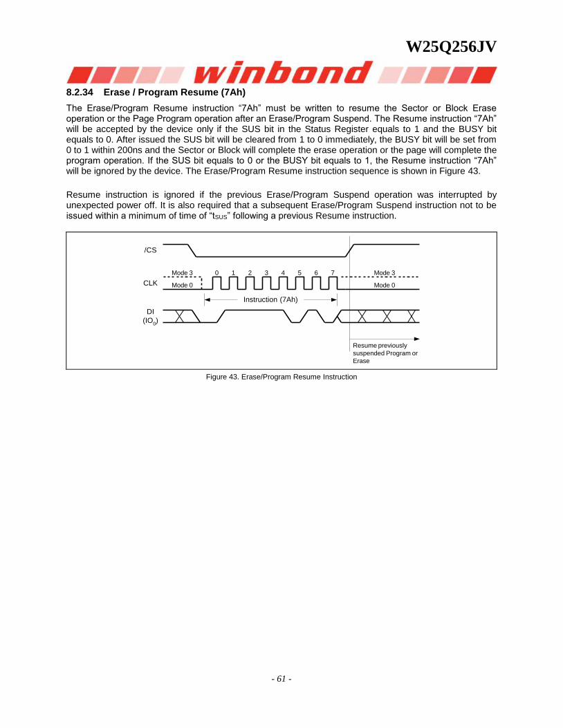
W25Q256JV
- 61 -
8.2.34 Erase / Program Resume (7Ah)
The Erase/Program Resume instruction “7Ah” must be written to resume the Sector or Block Erase operation or the Page Program operation after an Erase/Program Suspend. The Resume instruction “7Ah” will be accepted by the device only if the SUS bit in the Status Register equals to 1 and the BUSY bit equals to 0. After issued the SUS bit will be cleared from 1 to 0 immediately, the BUSY bit will be set from 0 to 1 within 200ns and the Sector or Block will complete the erase operation or the page will complete the program operation. If the SUS bit equals to 0 or the BUSY bit equals to 1, the Resume instruction “7Ah” will be ignored by the device. The Erase/Program Resume instruction sequence is shown in Figure 43.
Resume instruction is ignored if the previous Erase/Program Suspend operation was interrupted by unexpected power off. It is also required that a subsequent Erase/Program Suspend instruction not to be issued within a minimum of time of “tSUS” following a previous Resume instruction.
/CS
CLK
DI
(IO0)
Mode 0
Mode 3 0 1 2 3 4 5 6 7
Instruction (7Ah)
Mode 0
Mode 3
Resume previously
suspended Program or
Erase
Figure 43. Erase/Program Resume Instruction
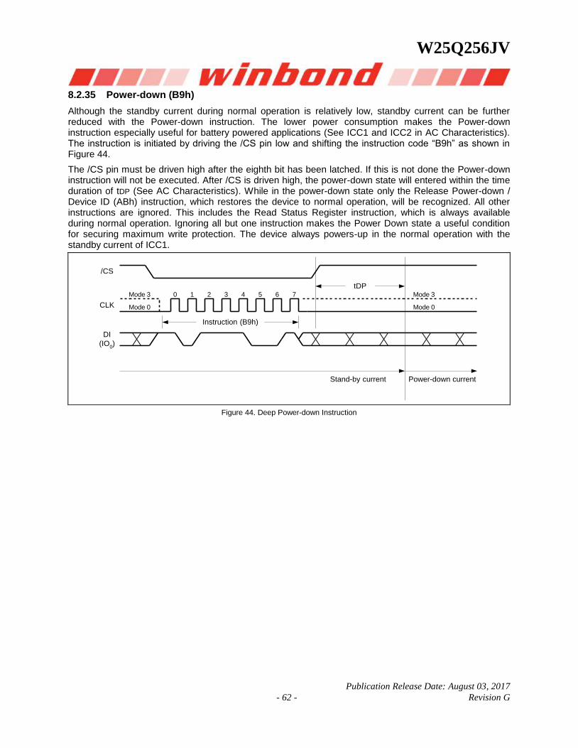
W25Q256JV
Publication Release Date: August 03, 2017
- 62 - Revision G
8.2.35 Power-down (B9h)
Although the standby current during normal operation is relatively low, standby current can be further reduced with the Power-down instruction. The lower power consumption makes the Power-down instruction especially useful for battery powered applications (See ICC1 and ICC2 in AC Characteristics). The instruction is initiated by driving the /CS pin low and shifting the instruction code “B9h” as shown in Figure 44.
The /CS pin must be driven high after the eighth bit has been latched. If this is not done the Power-down instruction will not be executed. After /CS is driven high, the power-down state will entered within the time duration of tDP (See AC Characteristics). While in the power-down state only the Release Power-down / Device ID (ABh) instruction, which restores the device to normal operation, will be recognized. All other instructions are ignored. This includes the Read Status Register instruction, which is always available during normal operation. Ignoring all but one instruction makes the Power Down state a useful condition for securing maximum write protection. The device always powers-up in the normal operation with the standby current of ICC1.
/CS
CLK
DI
(IO0)
Mode 0
Mode 3 0 1 2 3 4 5 6 7
Instruction (B9h)
Mode 0
Mode 3
tDP
Power-down currentStand-by current
Figure 44. Deep Power-down Instruction
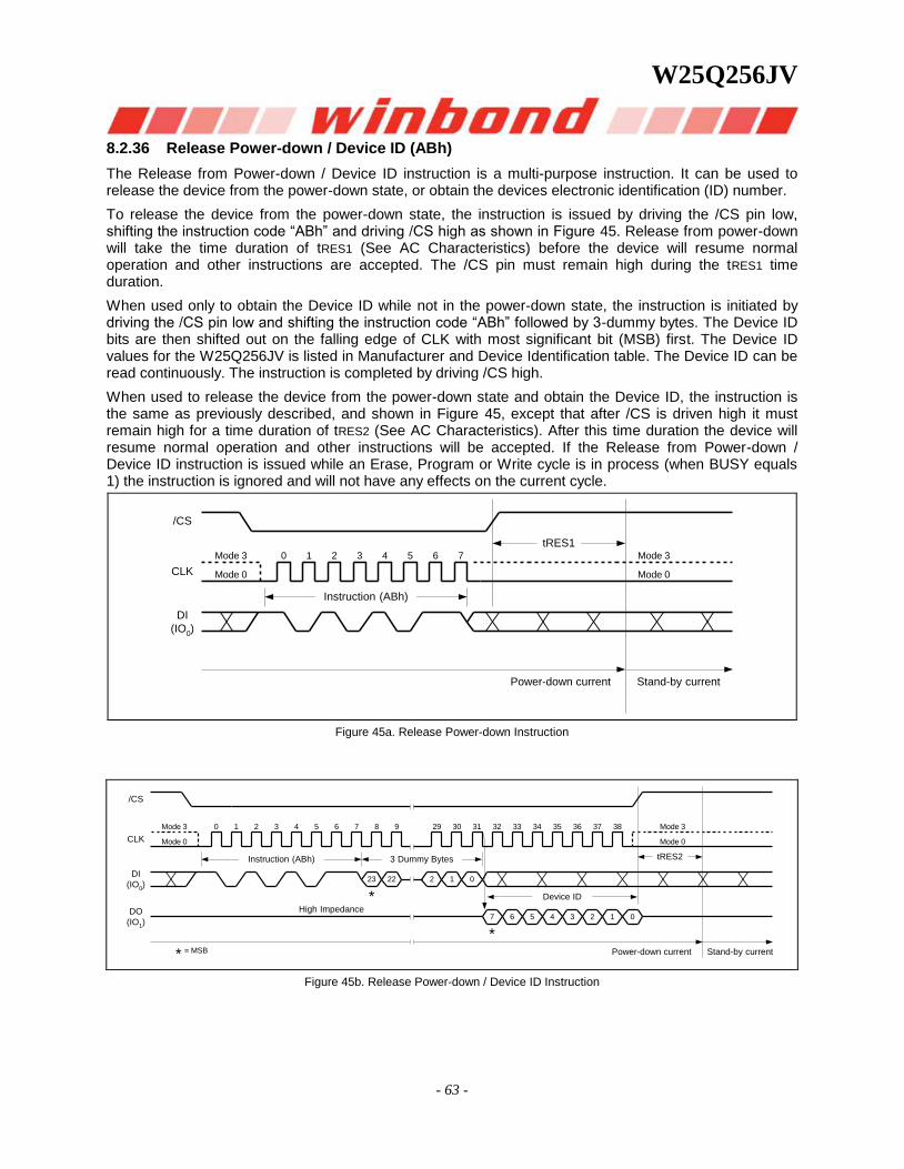
W25Q256JV
- 63 -
8.2.36 Release Power-down / Device ID (ABh)
The Release from Power-down / Device ID instruction is a multi-purpose instruction. It can be used to release the device from the power-down state, or obtain the devices electronic identification (ID) number.
To release the device from the power-down state, the instruction is issued by driving the /CS pin low, shifting the instruction code “ABh” and driving /CS high as shown in Figure 45. Release from power-down will take the time duration of tRES1 (See AC Characteristics) before the device will resume normal operation and other instructions are accepted. The /CS pin must remain high during the tRES1 time duration.
When used only to obtain the Device ID while not in the power-down state, the instruction is initiated by driving the /CS pin low and shifting the instruction code “ABh” followed by 3-dummy bytes. The Device ID bits are then shifted out on the falling edge of CLK with most significant bit (MSB) first. The Device ID values for the W25Q256JV is listed in Manufacturer and Device Identification table. The Device ID can be read continuously. The instruction is completed by driving /CS high.
When used to release the device from the power-down state and obtain the Device ID, the instruction is the same as previously described, and shown in Figure 45, except that after /CS is driven high it must remain high for a time duration of tRES2 (See AC Characteristics). After this time duration the device will resume normal operation and other instructions will be accepted. If the Release from Power-down / Device ID instruction is issued while an Erase, Program or Write cycle is in process (when BUSY equals 1) the instruction is ignored and will not have any effects on the current cycle.
/CS
CLK
DI
(IO0)
Mode 0
Mode 3 0 1 2 3 4 5 6 7
Instruction (ABh)
Mode 0
Mode 3
tRES1
Power-down current Stand-by current
Figure 45a. Release Power-down Instruction
tRES2
/CS
CLK
DI
(IO0)
DO
(IO1)
Mode 0
Mode 3 0 1 2 3 4 5 6 7
Instruction (ABh)
High Impedance
8 9 29 30 31
3 Dummy Bytes
23 22 2 1 0
*
Mode 0
Mode 3
7 6 5 4 3 2 1 0
*
32 33 34 35 36 37 38
Device ID
Power-down current Stand-by current= MSB*
Figure 45b. Release Power-down / Device ID Instruction
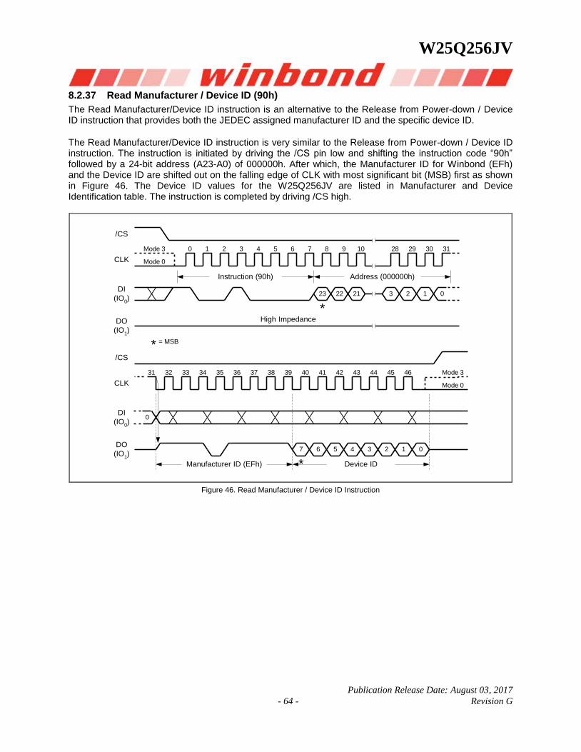
W25Q256JV
Publication Release Date: August 03, 2017
- 64 - Revision G
8.2.37 Read Manufacturer / Device ID (90h)
The Read Manufacturer/Device ID instruction is an alternative to the Release from Power-down / Device ID instruction that provides both the JEDEC assigned manufacturer ID and the specific device ID.
The Read Manufacturer/Device ID instruction is very similar to the Release from Power-down / Device ID instruction. The instruction is initiated by driving the /CS pin low and shifting the instruction code “90h” followed by a 24-bit address (A23-A0) of 000000h. After which, the Manufacturer ID for Winbond (EFh) and the Device ID are shifted out on the falling edge of CLK with most significant bit (MSB) first as shown in Figure 46. The Device ID values for the W25Q256JV are listed in Manufacturer and Device Identification table. The instruction is completed by driving /CS high.
/CS
CLK
DI
(IO0)
DO
(IO1)
Mode 0
Mode 3 0 1 2 3 4 5 6 7
Instruction (90h)
High Impedance
8 9 10 28 29 30 31
Address (000000h)
23 22 21 3 2 1 0
Device ID
*
/CS
CLK
DI
(IO0)
DO
(IO1)
32 33 34 35 36 37 38 39
Manufacturer ID (EFh)
40 41 42 44 45 46
7 6 5 4 3 2 1 0
*
4331
0
Mode 0
Mode 3
= MSB*
Figure 46. Read Manufacturer / Device ID Instruction
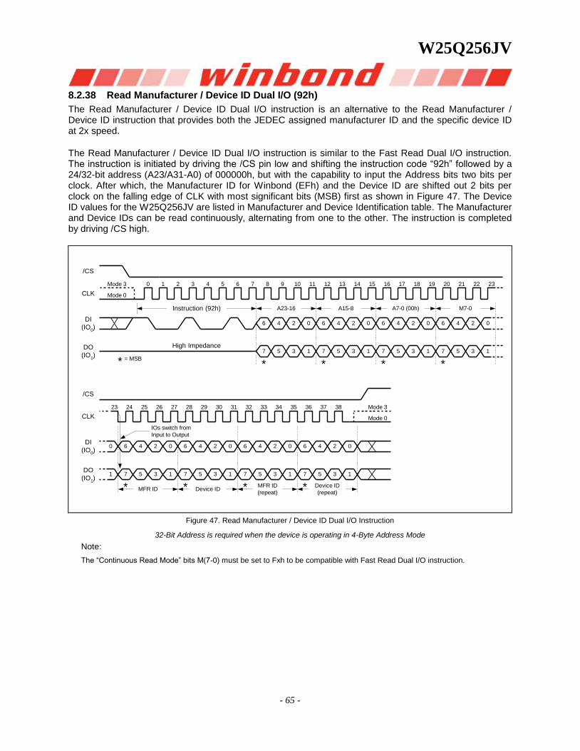
W25Q256JV
- 65 -
8.2.38 Read Manufacturer / Device ID Dual I/O (92h)
The Read Manufacturer / Device ID Dual I/O instruction is an alternative to the Read Manufacturer / Device ID instruction that provides both the JEDEC assigned manufacturer ID and the specific device ID at 2x speed.
The Read Manufacturer / Device ID Dual I/O instruction is similar to the Fast Read Dual I/O instruction. The instruction is initiated by driving the /CS pin low and shifting the instruction code “92h” followed by a 24/32-bit address (A23/A31-A0) of 000000h, but with the capability to input the Address bits two bits per clock. After which, the Manufacturer ID for Winbond (EFh) and the Device ID are shifted out 2 bits per clock on the falling edge of CLK with most significant bits (MSB) first as shown in Figure 47. The Device ID values for the W25Q256JV are listed in Manufacturer and Device Identification table. The Manufacturer and Device IDs can be read continuously, alternating from one to the other. The instruction is completed by driving /CS high.
/CS
CLK
DI
(IO0)
DO
(IO1)
Mode 0
Mode 3 0 1 2 3 4 5 6 7
Instruction (92h)
High Impedance
8 9 10 11 12 13 14 15 16 17 18 19 20 21 22
7 5 3 1
* *
6 4 2 0
7 5 3 1
6 4 2 0
7 5 3 1
6 4 2 0
7 5 3 1
6 4 2 0
23
* *
A23-16 A15-8 A7-0 (00h) M7-0
/CS
CLK
DI
(IO0)
DO
(IO1)
24 25 26 27 28 29 30 31 32 33 34 36 37 383523
0
Mode 0
Mode 3
7 5 3 1
6 4 2 0
7 5 3 1
6 4 2 0
7 5 3 1
6 4 2 0
7 5 3
6 4 2
1
0
1
MFR ID Device IDMFR ID
(repeat)
Device ID
(repeat)
IOs switch from
Input to Output
* ** *
= MSB*
Figure 47. Read Manufacturer / Device ID Dual I/O Instruction
32-Bit Address is required when the device is operating in 4-Byte Address Mode
Note:
The “Continuous Read Mode” bits M(7-0) must be set to Fxh to be compatible with Fast Read Dual I/O instruction.
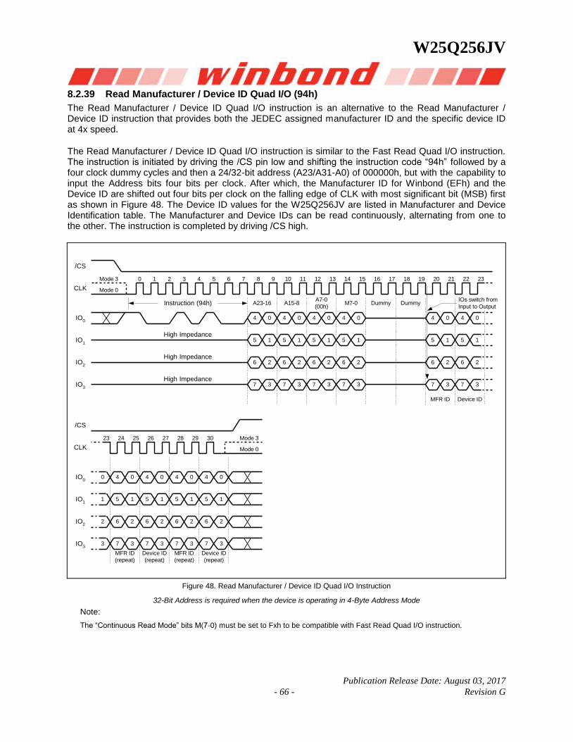
W25Q256JV
Publication Release Date: August 03, 2017
- 66 - Revision G
8.2.39 Read Manufacturer / Device ID Quad I/O (94h)
The Read Manufacturer / Device ID Quad I/O instruction is an alternative to the Read Manufacturer / Device ID instruction that provides both the JEDEC assigned manufacturer ID and the specific device ID at 4x speed.
The Read Manufacturer / Device ID Quad I/O instruction is similar to the Fast Read Quad I/O instruction. The instruction is initiated by driving the /CS pin low and shifting the instruction code “94h” followed by a four clock dummy cycles and then a 24/32-bit address (A23/A31-A0) of 000000h, but with the capability to input the Address bits four bits per clock. After which, the Manufacturer ID for Winbond (EFh) and the Device ID are shifted out four bits per clock on the falling edge of CLK with most significant bit (MSB) first as shown in Figure 48. The Device ID values for the W25Q256JV are listed in Manufacturer and Device Identification table. The Manufacturer and Device IDs can be read continuously, alternating from one to the other. The instruction is completed by driving /CS high.
Mode 0
Mode 3 0 1 2 3 4 5 6 7
Instruction (94h)
High Impedance
8 9 10 11 12 13 14 15 16 17 18 19 20 21 22
5 1
4 0
23
Mode 0
Mode 3
IOs switch from
Input to Output
High Impedance7 3
6 2
/CS
CLK
IO0
IO1
IO2
IO3
High Impedance
A23-16 A15-8A7-0
(00h)M7-0
MFR ID Device ID
Dummy Dummy
/CS
CLK
IO0
IO1
IO2
IO3
23
0
1
2
3
5 1
4 0
7 3
6 2
5 1
4 0
7 3
6 2
5 1
4 0
7 3
6 2
5 1
4 0
7 3
6 2
5 1
4 0
7 3
6 2
5 1
4 0
7 3
6 2
5 1
4 0
7 3
6 2
5 1
4 0
7 3
6 2
5 1
4 0
7 3
6 2
24 25 26 27 28 29 30
MFR ID
(repeat)
Device ID
(repeat)
MFR ID
(repeat)
Device ID
(repeat)
Figure 48. Read Manufacturer / Device ID Quad I/O Instruction
32-Bit Address is required when the device is operating in 4-Byte Address Mode
Note:
The “Continuous Read Mode” bits M(7-0) must be set to Fxh to be compatible with Fast Read Quad I/O instruction.
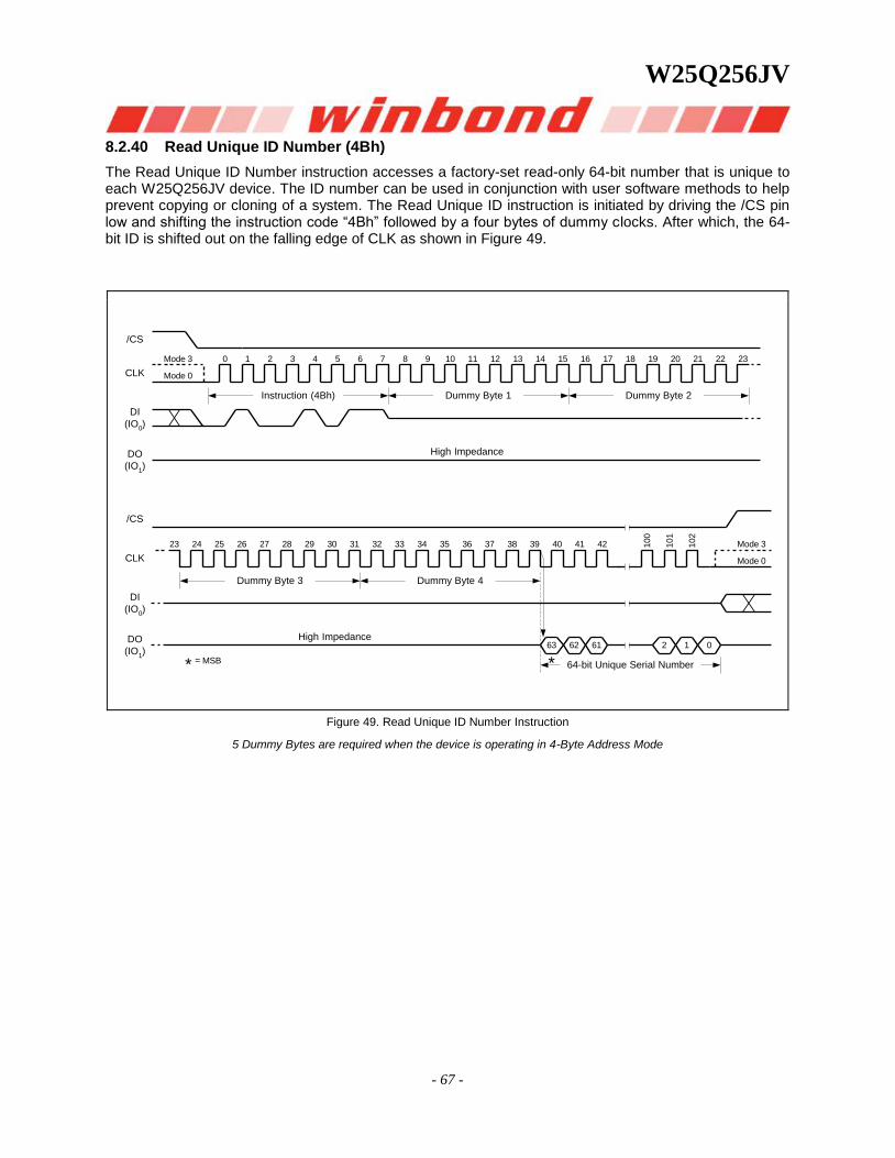
W25Q256JV
- 67 -
8.2.40 Read Unique ID Number (4Bh)
The Read Unique ID Number instruction accesses a factory-set read-only 64-bit number that is unique to each W25Q256JV device. The ID number can be used in conjunction with user software methods to help prevent copying or cloning of a system. The Read Unique ID instruction is initiated by driving the /CS pin low and shifting the instruction code “4Bh” followed by a four bytes of dummy clocks. After which, the 64-bit ID is shifted out on the falling edge of CLK as shown in Figure 49.
/CS
CLK
DI
(IO0)
DO
(IO1)
Mode 0
Mode 3 0 1 2 3 4 5 6 7
Instruction (4Bh)
High Impedance
8 9 10 11 12 13 14 15 16 17 18 19 20 21 22 23
/CS
CLK
DI
(IO0)
DO
(IO1)
24 25 26 27 28 29 30 31 32 33 34 36 37 383523
Mode 0
Mode 3
*
Dummy Byte 1 Dummy Byte 2
39 40 41 42
Dummy Byte 3 Dummy Byte 4
63 62 61 2 1 0
64-bit Unique Serial Number
100
101
102
High Impedance
= MSB*
Figure 49. Read Unique ID Number Instruction
5 Dummy Bytes are required when the device is operating in 4-Byte Address Mode
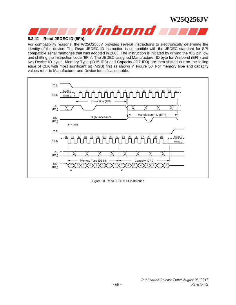
W25Q256JV
Publication Release Date: August 03, 2017
- 68 - Revision G
8.2.41 Read JEDEC ID (9Fh)
For compatibility reasons, the W25Q256JV provides several instructions to electronically determine the identity of the device. The Read JEDEC ID instruction is compatible with the JEDEC standard for SPI compatible serial memories that was adopted in 2003. The instruction is initiated by driving the /CS pin low and shifting the instruction code “9Fh”. The JEDEC assigned Manufacturer ID byte for Winbond (EFh) and two Device ID bytes, Memory Type (ID15-ID8) and Capacity (ID7-ID0) are then shifted out on the falling edge of CLK with most significant bit (MSB) first as shown in Figure 50. For memory type and capacity values refer to Manufacturer and Device Identification table.
/CS
CLK
DI
(IO0)
DO
(IO1)
Mode 0
Mode 3 0 1 2 3 4 5 6 7
Instruction (9Fh)
High Impedance
8 9 10 12 13 14 15
Capacity ID7-0
/CS
CLK
DI
(IO0)
DO
(IO1)
16 17 18 19 20 21 22 23
Manufacturer ID (EFh)
24 25 26 28 29 30
7 6 5 4 3 2 1 0
*
2715
Mode 0
Mode 3
11
7 6 5 4 3 2 1 0
*
Memory Type ID15-8
= MSB*
Figure 50. Read JEDEC ID Instruction
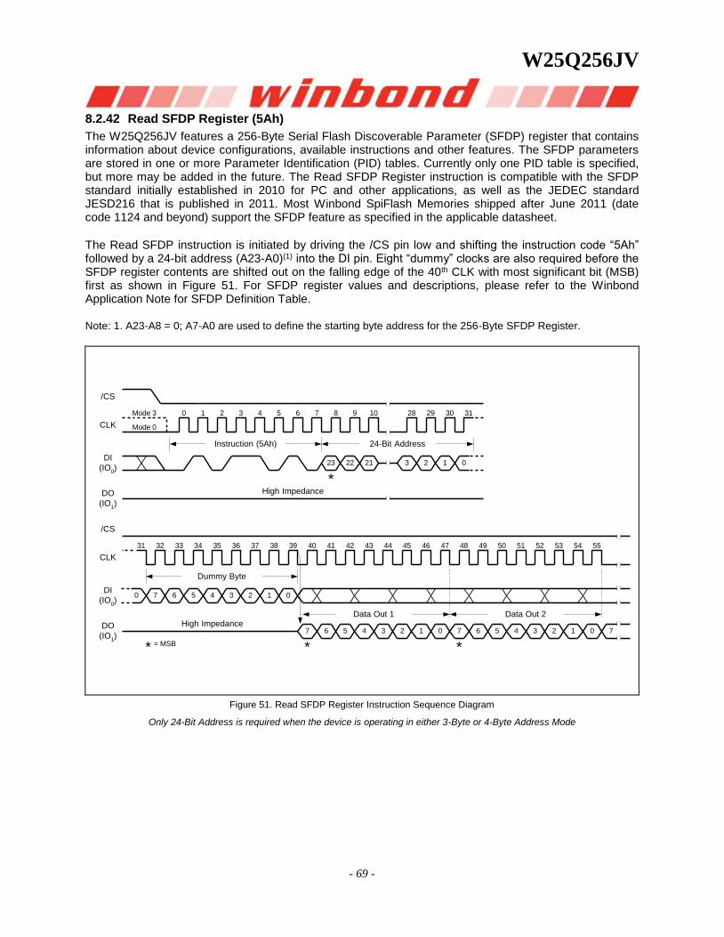
W25Q256JV
- 69 -
8.2.42 Read SFDP Register (5Ah)
The W25Q256JV features a 256-Byte Serial Flash Discoverable Parameter (SFDP) register that contains information about device configurations, available instructions and other features. The SFDP parameters are stored in one or more Parameter Identification (PID) tables. Currently only one PID table is specified, but more may be added in the future. The Read SFDP Register instruction is compatible with the SFDP standard initially established in 2010 for PC and other applications, as well as the JEDEC standard JESD216 that is published in 2011. Most Winbond SpiFlash Memories shipped after June 2011 (date code 1124 and beyond) support the SFDP feature as specified in the applicable datasheet.
The Read SFDP instruction is initiated by driving the /CS pin low and shifting the instruction code “5Ah” followed by a 24-bit address (A23-A0)(1) into the DI pin. Eight “dummy” clocks are also required before the SFDP register contents are shifted out on the falling edge of the 40th CLK with most significant bit (MSB) first as shown in Figure 51. For SFDP register values and descriptions, please refer to the Winbond Application Note for SFDP Definition Table.
Note: 1. A23-A8 = 0; A7-A0 are used to define the starting byte address for the 256-Byte SFDP Register.
/CS
CLK
DI
(IO0)
DO
(IO1)
Mode 0
Mode 3 0 1 2 3 4 5 6 7
Instruction (5Ah)
High Impedance
8 9 10 28 29 30 31
24-Bit Address
23 22 21 3 2 1 0
Data Out 1
*
/CS
CLK
DI
(IO0)
DO
(IO1)
32 33 34 35 36 37 38 39
Dummy Byte
High Impedance
40 41 42 44 45 46 47 48 49 50 51 52 53 54 55
7 6 5 4 3 2 1 0 7
Data Out 2
*
7 6 5 4 3 2 1 0
*
7 6 5 4 3 2 1 0
4331
0
= MSB*
Figure 51. Read SFDP Register Instruction Sequence Diagram
Only 24-Bit Address is required when the device is operating in either 3-Byte or 4-Byte Address Mode
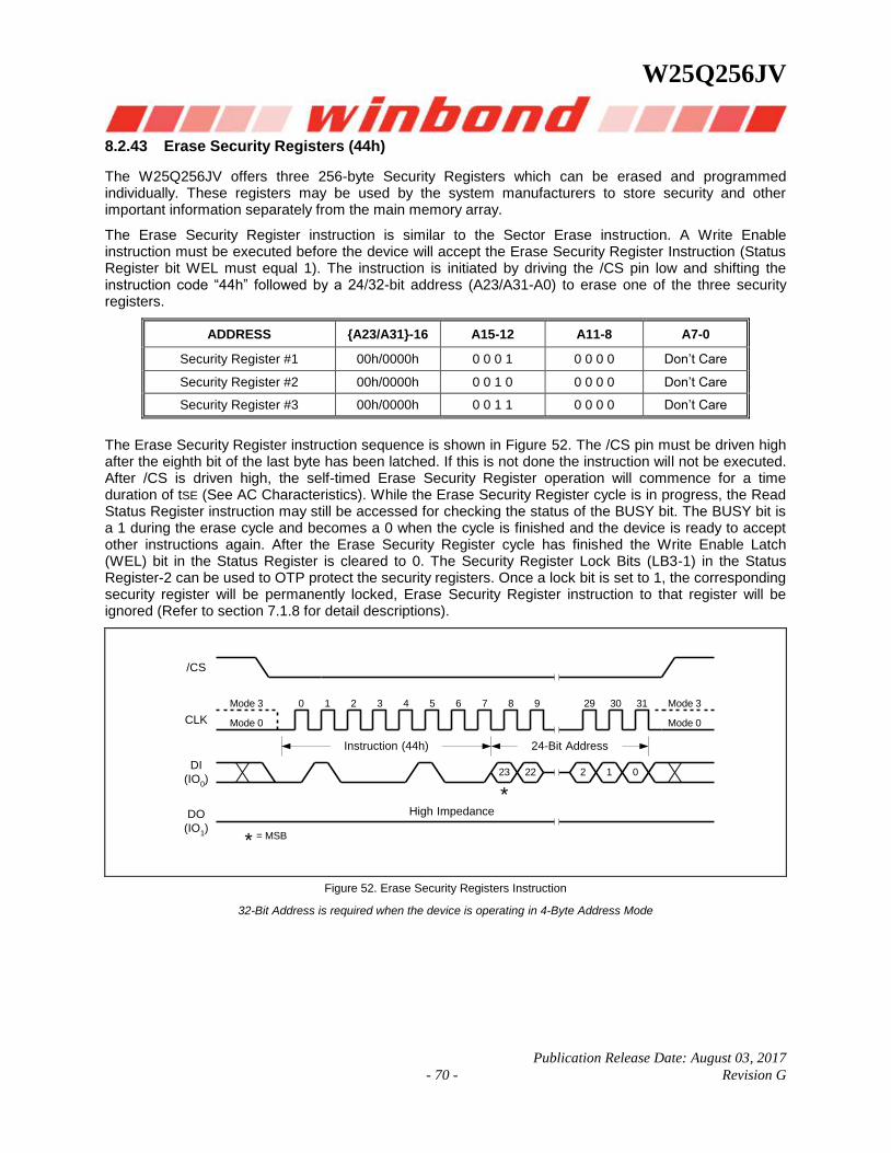
W25Q256JV
Publication Release Date: August 03, 2017
- 70 - Revision G
8.2.43 Erase Security Registers (44h)
The W25Q256JV offers three 256-byte Security Registers which can be erased and programmed individually. These registers may be used by the system manufacturers to store security and other important information separately from the main memory array.
The Erase Security Register instruction is similar to the Sector Erase instruction. A Write Enable instruction must be executed before the device will accept the Erase Security Register Instruction (Status Register bit WEL must equal 1). The instruction is initiated by driving the /CS pin low and shifting the instruction code “44h” followed by a 24/32-bit address (A23/A31-A0) to erase one of the three security registers.
ADDRESS {A23/A31}-16 A15-12 A11-8 A7-0
Security Register #1 00h/0000h 0 0 0 1 0 0 0 0 Don’t Care
Security Register #2 00h/0000h 0 0 1 0 0 0 0 0 Don’t Care
Security Register #3 00h/0000h 0 0 1 1 0 0 0 0 Don’t Care
The Erase Security Register instruction sequence is shown in Figure 52. The /CS pin must be driven high after the eighth bit of the last byte has been latched. If this is not done the instruction will not be executed. After /CS is driven high, the self-timed Erase Security Register operation will commence for a time duration of tSE (See AC Characteristics). While the Erase Security Register cycle is in progress, the Read Status Register instruction may still be accessed for checking the status of the BUSY bit. The BUSY bit is a 1 during the erase cycle and becomes a 0 when the cycle is finished and the device is ready to accept other instructions again. After the Erase Security Register cycle has finished the Write Enable Latch (WEL) bit in the Status Register is cleared to 0. The Security Register Lock Bits (LB3-1) in the Status Register-2 can be used to OTP protect the security registers. Once a lock bit is set to 1, the corresponding security register will be permanently locked, Erase Security Register instruction to that register will be ignored (Refer to section 7.1.8 for detail descriptions).
/CS
CLK
DI
(IO0)
DO
(IO1)
Mode 0
Mode 3 0 1 2 3 4 5 6 7
Instruction (44h)
High Impedance
8 9 29 30 31
24-Bit Address
23 22 2 1 0
*
Mode 0
Mode 3
= MSB*
Figure 52. Erase Security Registers Instruction
32-Bit Address is required when the device is operating in 4-Byte Address Mode
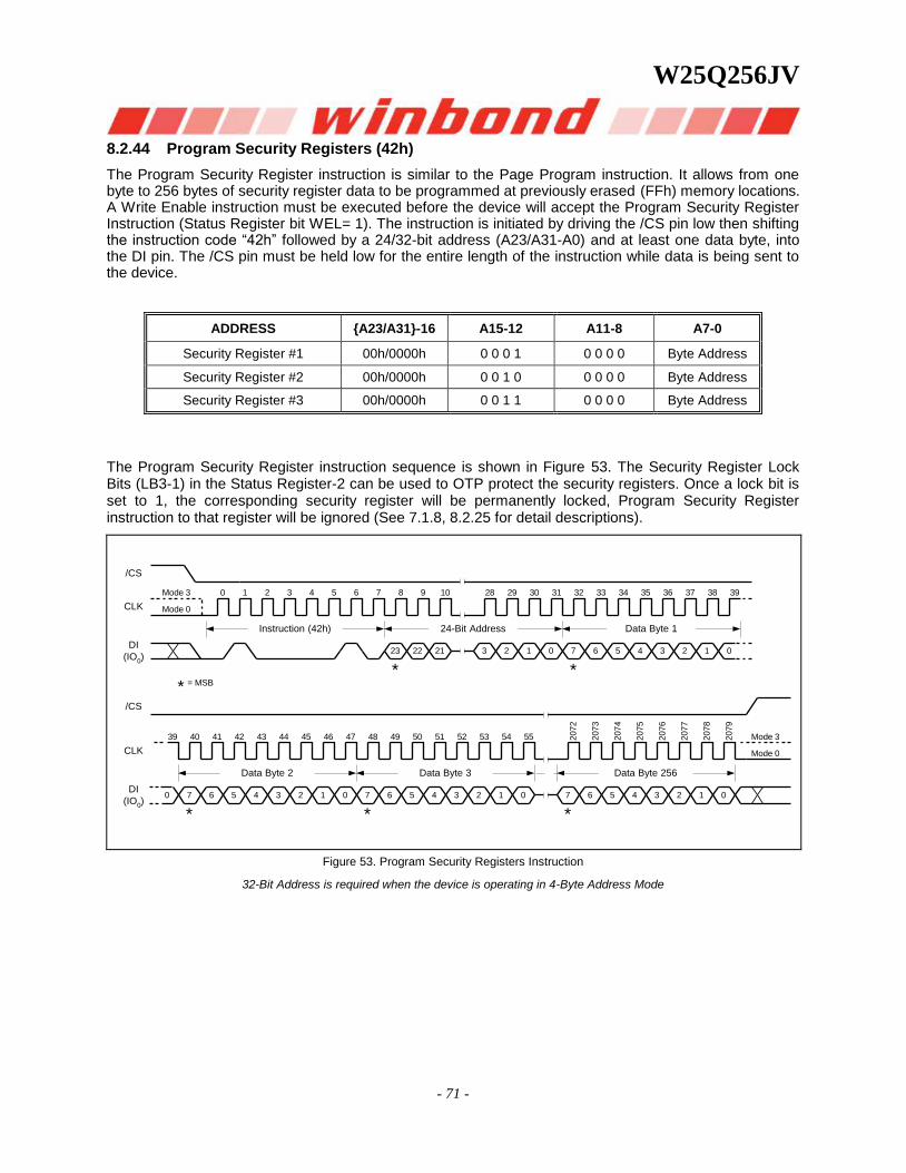
W25Q256JV
- 71 -
8.2.44 Program Security Registers (42h)
The Program Security Register instruction is similar to the Page Program instruction. It allows from one byte to 256 bytes of security register data to be programmed at previously erased (FFh) memory locations. A Write Enable instruction must be executed before the device will accept the Program Security Register Instruction (Status Register bit WEL= 1). The instruction is initiated by driving the /CS pin low then shifting the instruction code “42h” followed by a 24/32-bit address (A23/A31-A0) and at least one data byte, into the DI pin. The /CS pin must be held low for the entire length of the instruction while data is being sent to the device.
ADDRESS {A23/A31}-16 A15-12 A11-8 A7-0
Security Register #1 00h/0000h 0 0 0 1 0 0 0 0 Byte Address
Security Register #2 00h/0000h 0 0 1 0 0 0 0 0 Byte Address
Security Register #3 00h/0000h 0 0 1 1 0 0 0 0 Byte Address
The Program Security Register instruction sequence is shown in Figure 53. The Security Register Lock Bits (LB3-1) in the Status Register-2 can be used to OTP protect the security registers. Once a lock bit is set to 1, the corresponding security register will be permanently locked, Program Security Register instruction to that register will be ignored (See 7.1.8, 8.2.25 for detail descriptions).
/CS
CLK
DI
(IO0)
Mode 0
Mode 3 0 1 2 3 4 5 6 7
Instruction (42h)
8 9 10 28 29 30 39
24-Bit Address
23 22 21 3 2 1
*
/CS
CLK
DI
(IO0)
40 41 42 43 44 45 46 47
Data Byte 2
48 49 50 52 53 54 55 2072
7 6 5 4 3 2 1 0
5139
0
31
0
32 33 34 35 36 37 38
Data Byte 1
7 6 5 4 3 2 1
*
Mode 0
Mode 3
Data Byte 3
2073
2074
2075
2076
2077
2078
2079
0
Data Byte 256
*
7 6 5 4 3 2 1 0
*
7 6 5 4 3 2 1 0
*
= MSB*
Figure 53. Program Security Registers Instruction
32-Bit Address is required when the device is operating in 4-Byte Address Mode
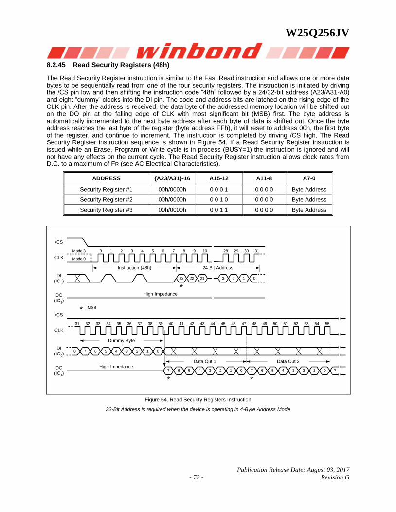
W25Q256JV
Publication Release Date: August 03, 2017
- 72 - Revision G
8.2.45 Read Security Registers (48h)
The Read Security Register instruction is similar to the Fast Read instruction and allows one or more data bytes to be sequentially read from one of the four security registers. The instruction is initiated by driving the /CS pin low and then shifting the instruction code “48h” followed by a 24/32-bit address (A23/A31-A0) and eight “dummy” clocks into the DI pin. The code and address bits are latched on the rising edge of the CLK pin. After the address is received, the data byte of the addressed memory location will be shifted out on the DO pin at the falling edge of CLK with most significant bit (MSB) first. The byte address is automatically incremented to the next byte address after each byte of data is shifted out. Once the byte address reaches the last byte of the register (byte address FFh), it will reset to address 00h, the first byte of the register, and continue to increment. The instruction is completed by driving /CS high. The Read Security Register instruction sequence is shown in Figure 54. If a Read Security Register instruction is issued while an Erase, Program or Write cycle is in process (BUSY=1) the instruction is ignored and will not have any effects on the current cycle. The Read Security Register instruction allows clock rates from D.C. to a maximum of FR (see AC Electrical Characteristics).
ADDRESS {A23/A31}-16 A15-12 A11-8 A7-0
Security Register #1 00h/0000h 0 0 0 1 0 0 0 0 Byte Address
Security Register #2 00h/0000h 0 0 1 0 0 0 0 0 Byte Address
Security Register #3 00h/0000h 0 0 1 1 0 0 0 0 Byte Address
/CS
CLK
DI
(IO0)
DO
(IO1)
Mode 0
Mode 3 0 1 2 3 4 5 6 7
Instruction (48h)
High Impedance
8 9 10 28 29 30 31
24-Bit Address
23 22 21 3 2 1 0
Data Out 1
*
/CS
CLK
DI
(IO0)
DO
(IO1)
32 33 34 35 36 37 38 39
Dummy Byte
High Impedance
40 41 42 44 45 46 47 48 49 50 51 52 53 54 55
7 6 5 4 3 2 1 0 7
Data Out 2
*
7 6 5 4 3 2 1 0
*
7 6 5 4 3 2 1 0
4331
0
= MSB*
Figure 54. Read Security Registers Instruction
32-Bit Address is required when the device is operating in 4-Byte Address Mode
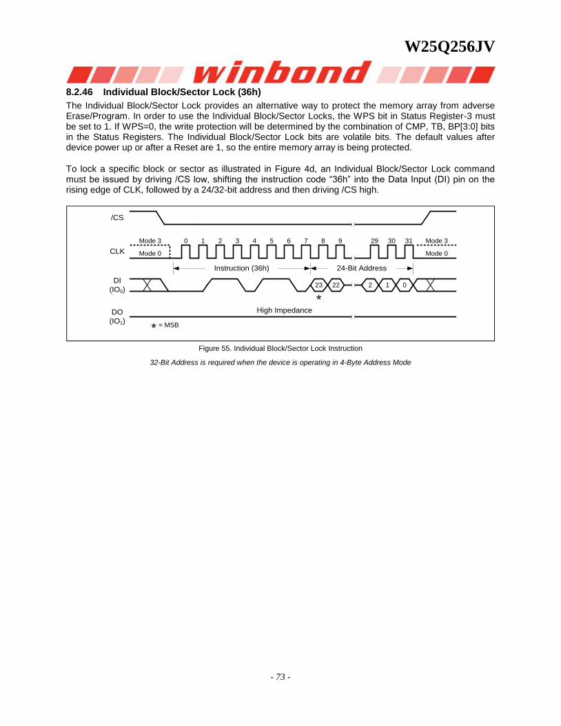
W25Q256JV
- 73 -
8.2.46 Individual Block/Sector Lock (36h)
The Individual Block/Sector Lock provides an alternative way to protect the memory array from adverse Erase/Program. In order to use the Individual Block/Sector Locks, the WPS bit in Status Register-3 must be set to 1. If WPS=0, the write protection will be determined by the combination of CMP, TB, BP[3:0] bits in the Status Registers. The Individual Block/Sector Lock bits are volatile bits. The default values after device power up or after a Reset are 1, so the entire memory array is being protected.
To lock a specific block or sector as illustrated in Figure 4d, an Individual Block/Sector Lock command must be issued by driving /CS low, shifting the instruction code “36h” into the Data Input (DI) pin on the rising edge of CLK, followed by a 24/32-bit address and then driving /CS high.
/CS
CLK
DI
(IO0)
DO
(IO1)
Mode 0
Mode 3 0 1 2 3 4 5 6 7
Instruction (36h)
High Impedance
8 9 29 30 31
24-Bit Address
23 22 2 1 0
*
Mode 0
Mode 3
= MSB*
Figure 55. Individual Block/Sector Lock Instruction
32-Bit Address is required when the device is operating in 4-Byte Address Mode
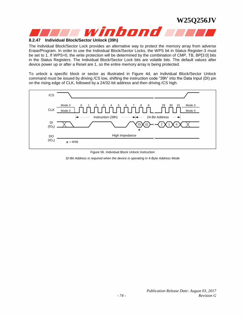
W25Q256JV
Publication Release Date: August 03, 2017
- 74 - Revision G
8.2.47 Individual Block/Sector Unlock (39h)
The Individual Block/Sector Lock provides an alternative way to protect the memory array from adverse Erase/Program. In order to use the Individual Block/Sector Locks, the WPS bit in Status Register-3 must be set to 1. If WPS=0, the write protection will be determined by the combination of CMP, TB, BP[3:0] bits in the Status Registers. The Individual Block/Sector Lock bits are volatile bits. The default values after device power up or after a Reset are 1, so the entire memory array is being protected.
To unlock a specific block or sector as illustrated in Figure 4d, an Individual Block/Sector Unlock command must be issued by driving /CS low, shifting the instruction code “39h” into the Data Input (DI) pin on the rising edge of CLK, followed by a 24/32-bit address and then driving /CS high.
/CS
CLK
DI
(IO0)
DO
(IO1)
Mode 0
Mode 3 0 1 2 3 4 5 6 7
Instruction (39h)
High Impedance
8 9 29 30 31
24-Bit Address
23 22 2 1 0
*
Mode 0
Mode 3
= MSB*
Figure 56. Individual Block Unlock Instruction
32-Bit Address is required when the device is operating in 4-Byte Address Mode
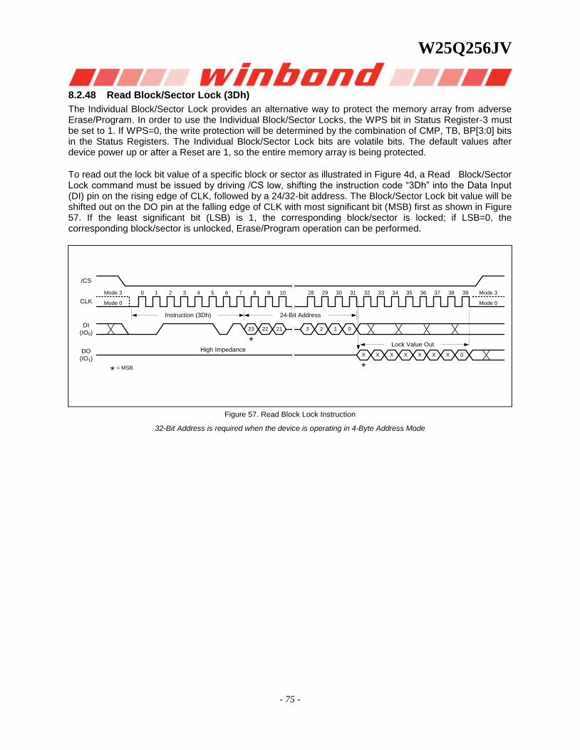
W25Q256JV
- 75 -
8.2.48 Read Block/Sector Lock (3Dh)
The Individual Block/Sector Lock provides an alternative way to protect the memory array from adverse Erase/Program. In order to use the Individual Block/Sector Locks, the WPS bit in Status Register-3 must be set to 1. If WPS=0, the write protection will be determined by the combination of CMP, TB, BP[3:0] bits in the Status Registers. The Individual Block/Sector Lock bits are volatile bits. The default values after device power up or after a Reset are 1, so the entire memory array is being protected.
To read out the lock bit value of a specific block or sector as illustrated in Figure 4d, a Read Block/Sector Lock command must be issued by driving /CS low, shifting the instruction code “3Dh” into the Data Input (DI) pin on the rising edge of CLK, followed by a 24/32-bit address. The Block/Sector Lock bit value will be shifted out on the DO pin at the falling edge of CLK with most significant bit (MSB) first as shown in Figure 57. If the least significant bit (LSB) is 1, the corresponding block/sector is locked; if LSB=0, the corresponding block/sector is unlocked, Erase/Program operation can be performed.
/CS
CLK
DI
(IO0)
DO
(IO1)
Mode 0
Mode 3 0 1 2 3 4 5 6 7
Instruction (3Dh)
High Impedance
8 9 10 28 29 30 31 32 33 34 35 36 37 38 39
X X X X X X X 0
24-Bit Address
23 22 21 3 2 1 0
Lock Value Out
*
*
= MSB*
Mode 0
Mode 3
Figure 57. Read Block Lock Instruction
32-Bit Address is required when the device is operating in 4-Byte Address Mode
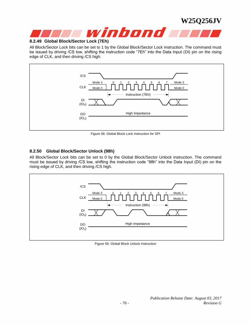
W25Q256JV
Publication Release Date: August 03, 2017
- 76 - Revision G
8.2.49 Global Block/Sector Lock (7Eh)
All Block/Sector Lock bits can be set to 1 by the Global Block/Sector Lock instruction. The command must be issued by driving /CS low, shifting the instruction code “7Eh” into the Data Input (DI) pin on the rising edge of CLK, and then driving /CS high.
/CS
CLK
DI
(IO0)
DO
(IO1)
Mode 0
Mode 3 0 1 2 3 4 5 6 7
Mode 0
Mode 3
Instruction (7Eh)
High Impedance
Figure 58. Global Block Lock Instruction for SPI
8.2.50 Global Block/Sector Unlock (98h)
All Block/Sector Lock bits can be set to 0 by the Global Block/Sector Unlock instruction. The command must be issued by driving /CS low, shifting the instruction code “98h” into the Data Input (DI) pin on the rising edge of CLK, and then driving /CS high.
/CS
CLK
DI
(IO0)
DO
(IO1)
Mode 0
Mode 3 0 1 2 3 4 5 6 7
Mode 0
Mode 3
Instruction (98h)
High Impedance
Figure 59. Global Block Unlock Instruction
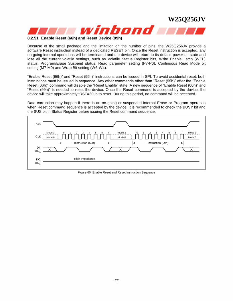
W25Q256JV
- 77 -
8.2.51 Enable Reset (66h) and Reset Device (99h)
Because of the small package and the limitation on the number of pins, the W25Q256JV provide a software Reset instruction instead of a dedicated RESET pin. Once the Reset instruction is accepted, any on-going internal operations will be terminated and the device will return to its default power-on state and lose all the current volatile settings, such as Volatile Status Register bits, Write Enable Latch (WEL) status, Program/Erase Suspend status, Read parameter setting (P7-P0), Continuous Read Mode bit setting (M7-M0) and Wrap Bit setting (W6-W4).
“Enable Reset (66h)” and “Reset (99h)” instructions can be issued in SPI. To avoid accidental reset, both instructions must be issued in sequence. Any other commands other than “Reset (99h)” after the “Enable Reset (66h)” command will disable the “Reset Enable” state. A new sequence of “Enable Reset (66h)” and “Reset (99h)” is needed to reset the device. Once the Reset command is accepted by the device, the device will take approximately tRST=30us to reset. During this period, no command will be accepted.
Data corruption may happen if there is an on-going or suspended internal Erase or Program operation when Reset command sequence is accepted by the device. It is recommended to check the BUSY bit and the SUS bit in Status Register before issuing the Reset command sequence.
Mode 0
Mode 3 0 1 2 3 4 5 6 7
Instruction (99h)
Mode 0
Mode 3
/CS
CLK
DI
(IO0)
DO
(IO1)
Mode 0
Mode 3 0 1 2 3 4 5 6 7
Instruction (66h)
High Impedance
Figure 60. Enable Reset and Reset Instruction Sequence
W25Q256JV
Publication Release Date: August 03, 2017
- 78 - Revision G
9. ELECTRICAL CHARACTERISTICS
9.1 Absolute Maximum Ratings (1)
PARAMETERS SYMBOL CONDITIONS RANGE UNIT
Supply Voltage VCC –0.6 to +4.6 V
Voltage Applied to Any Pin VIO Relative to Ground –0.6 to VCC+0.4 V
Transient Voltage on any Pin VIOT <20nS Transient
Relative to Ground –2.0 to VCC+2.0 V
Storage Temperature TSTG –65 to +150 °C
Lead Temperature TLEAD See Note (2) °C
Electrostatic Discharge Voltage VESD Human Body Model(3) –2000 to +2000 V
Notes:
1. This device has been designed and tested for the specified operation ranges. Proper operation outside of these levels is not guaranteed. Exposure to absolute maximum ratings may affect device reliability. Exposure beyond absolute maximum ratings may cause permanent damage.
2. Compliant with JEDEC Standard J-STD-20C for small body Sn-Pb or Pb-free (Green) assembly and the European directive on restrictions on hazardous substances (RoHS) 2002/95/EU.
3. JEDEC Std JESD22-A114A (C1=100pF, R1=1500 ohms, R2=500 ohms).
9.2 Operating Ranges
PARAMETER SYMBOL CONDITIONS SPEC
UNIT MIN MAX
Supply Voltage(1) VCC FR = 133MHz, fR = 50MHz 3.0 3.6 V
FR = 104MHz, fR = 50MHz 2.7 3.0 V
Ambient Temperature, Operating
TA Industrial –40 +85 °C
Note:
1. VCC voltage during Read can operate across the min and max range but should not exceed ±10% of the programming (erase/write) voltage.
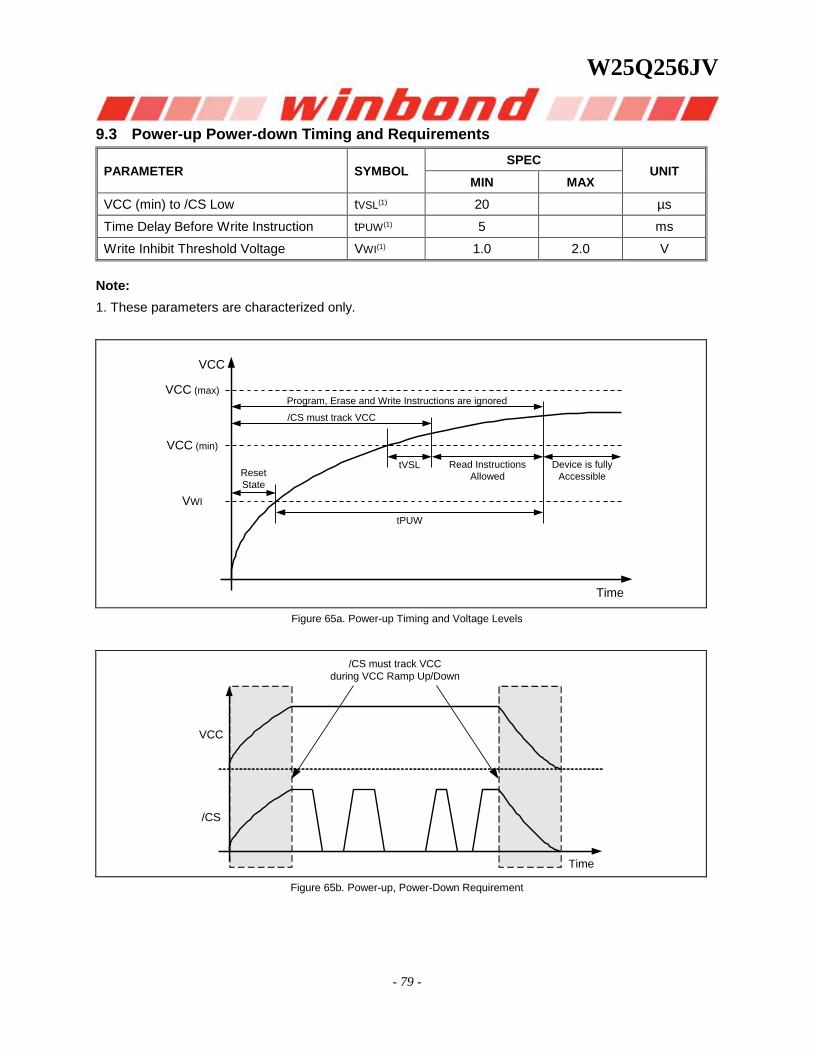
W25Q256JV
- 79 -
9.3 Power-up Power-down Timing and Requirements
PARAMETER SYMBOL SPEC
UNIT MIN MAX
VCC (min) to /CS Low tVSL(1) 20 µs
Time Delay Before Write Instruction tPUW(1) 5 ms
Write Inhibit Threshold Voltage VWI(1) 1.0 2.0 V
Note:
1. These parameters are characterized only.
VCC
tVSL Read Instructions
Allowed
Device is fully
Accessible
tPUW
/CS must track VCC
Program, Erase and Write Instructions are ignored
Reset
State
VCC (max)
VCC (min)
VWI
Time
Figure 65a. Power-up Timing and Voltage Levels
VCC
Time
/CS must track VCC
during VCC Ramp Up/Down
/CS
Figure 65b. Power-up, Power-Down Requirement
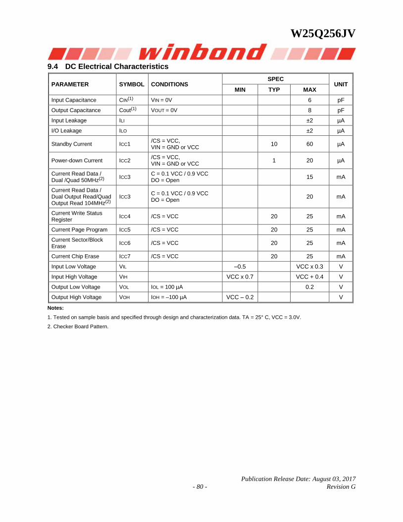
W25Q256JV
Publication Release Date: August 03, 2017
- 80 - Revision G
9.4 DC Electrical Characteristics
PARAMETER SYMBOL CONDITIONS SPEC
UNIT MIN TYP MAX
Input Capacitance CIN(1) VIN = 0V 6 pF
Output Capacitance Cout(1) VOUT = 0V 8 pF
Input Leakage ILI ±2 µA
I/O Leakage ILO ±2 µA
Standby Current ICC1 /CS = VCC, VIN = GND or VCC
10 60 µA
Power-down Current ICC2 /CS = VCC, VIN = GND or VCC
1 20 µA
Current Read Data / Dual /Quad 50MHz(2)
ICC3 C = 0.1 VCC / 0.9 VCC DO = Open
15 mA
Current Read Data / Dual Output Read/Quad Output Read 104MHz(2)
ICC3 C = 0.1 VCC / 0.9 VCC DO = Open 20 mA
Current Write Status Register
ICC4 /CS = VCC 20 25 mA
Current Page Program ICC5 /CS = VCC 20 25 mA
Current Sector/Block Erase
ICC6 /CS = VCC 20 25 mA
Current Chip Erase ICC7 /CS = VCC 20 25 mA
Input Low Voltage VIL –0.5 VCC x 0.3 V
Input High Voltage VIH VCC x 0.7 VCC + 0.4 V
Output Low Voltage VOL IOL = 100 µA 0.2 V
Output High Voltage VOH IOH = –100 µA VCC – 0.2 V
Notes:
1. Tested on sample basis and specified through design and characterization data. TA = 25° C, VCC = 3.0V.
2. Checker Board Pattern.
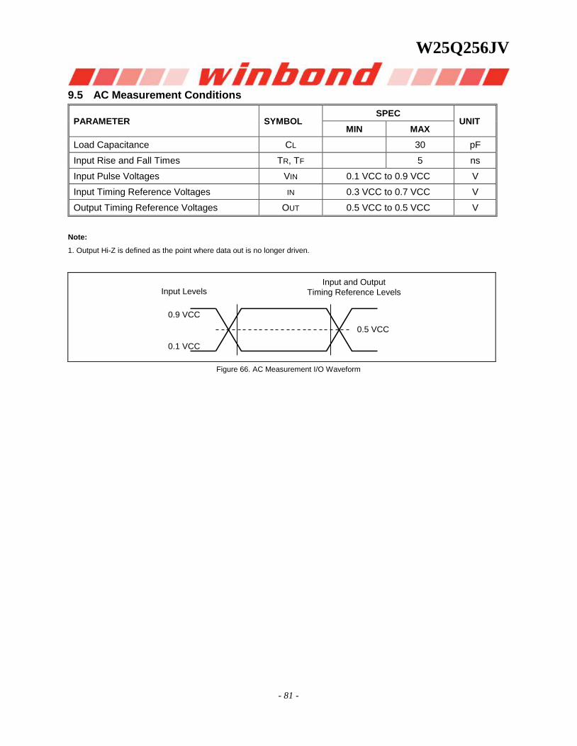
W25Q256JV
- 81 -
9.5 AC Measurement Conditions
PARAMETER SYMBOL SPEC
UNIT MIN MAX
Load Capacitance CL 30 pF
Input Rise and Fall Times TR, TF 5 ns
Input Pulse Voltages VIN 0.1 VCC to 0.9 VCC V
Input Timing Reference Voltages IN 0.3 VCC to 0.7 VCC V
Output Timing Reference Voltages OUT 0.5 VCC to 0.5 VCC V
Note:
1. Output Hi-Z is defined as the point where data out is no longer driven.
Input and Output
Timing Reference LevelsInput Levels
0.9 VCC
0.1 VCC
0.5 VCC
Figure 66. AC Measurement I/O Waveform
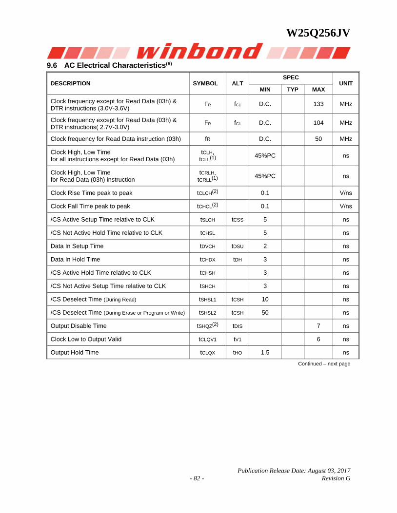
W25Q256JV
Publication Release Date: August 03, 2017
- 82 - Revision G
9.6 AC Electrical Characteristics(6)
DESCRIPTION SYMBOL ALT SPEC
UNIT MIN TYP MAX
Clock frequency except for Read Data (03h) & DTR instructions (3.0V-3.6V)
FR fC1 D.C. 133 MHz
Clock frequency except for Read Data (03h) & DTR instructions( 2.7V-3.0V)
FR fC1 D.C. 104 MHz
Clock frequency for Read Data instruction (03h) fR D.C. 50 MHz
Clock High, Low Time for all instructions except for Read Data (03h)
tCLH,
tCLL(1)
45%PC ns
Clock High, Low Time for Read Data (03h) instruction
tCRLH, tCRLL(1)
45%PC ns
Clock Rise Time peak to peak tCLCH(2) 0.1 V/ns
Clock Fall Time peak to peak tCHCL(2) 0.1 V/ns
/CS Active Setup Time relative to CLK tSLCH tCSS 5 ns
/CS Not Active Hold Time relative to CLK tCHSL 5 ns
Data In Setup Time tDVCH tDSU 2 ns
Data In Hold Time tCHDX tDH 3 ns
/CS Active Hold Time relative to CLK tCHSH 3 ns
/CS Not Active Setup Time relative to CLK tSHCH 3 ns
/CS Deselect Time (During Read) tSHSL1 tCSH 10 ns
/CS Deselect Time (During Erase or Program or Write) tSHSL2 tCSH 50 ns
Output Disable Time tSHQZ(2) tDIS 7 ns
Clock Low to Output Valid tCLQV1 tV1 6 ns
Output Hold Time tCLQX tHO 1.5 ns
Continued – next page
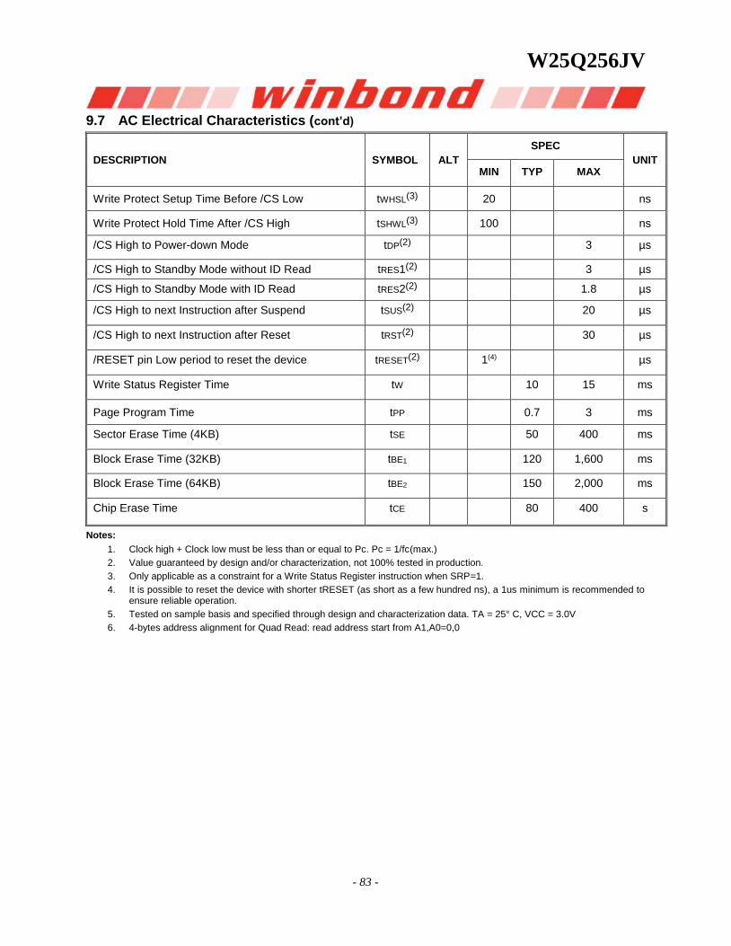
W25Q256JV
- 83 -
9.7 AC Electrical Characteristics (cont’d)
DESCRIPTION SYMBOL ALT
SPEC
UNIT MIN TYP MAX
Write Protect Setup Time Before /CS Low tWHSL(3) 20 ns
Write Protect Hold Time After /CS High tSHWL(3) 100 ns
/CS High to Power-down Mode tDP(2) 3 µs
/CS High to Standby Mode without ID Read tRES1(2) 3 µs
/CS High to Standby Mode with ID Read tRES2(2) 1.8 µs
/CS High to next Instruction after Suspend tSUS(2) 20 µs
/CS High to next Instruction after Reset tRST(2) 30 µs
/RESET pin Low period to reset the device tRESET(2) 1(4) µs
Write Status Register Time tW 10 15 ms
Page Program Time tPP 0.7 3 ms
Sector Erase Time (4KB) tSE 50 400 ms
Block Erase Time (32KB) tBE1 120 1,600 ms
Block Erase Time (64KB) tBE2 150 2,000 ms
Chip Erase Time tCE 80 400 s
Notes:
1. Clock high + Clock low must be less than or equal to Pc. Pc = 1/fc(max.)
2. Value guaranteed by design and/or characterization, not 100% tested in production.
3. Only applicable as a constraint for a Write Status Register instruction when SRP=1.
4. It is possible to reset the device with shorter tRESET (as short as a few hundred ns), a 1us minimum is recommended to ensure reliable operation.
5. Tested on sample basis and specified through design and characterization data. TA = 25° C, VCC = 3.0V
6. 4-bytes address alignment for Quad Read: read address start from A1,A0=0,0
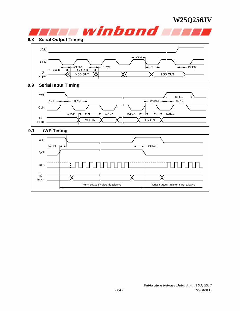
W25Q256JV
Publication Release Date: August 03, 2017
- 84 - Revision G
9.8 Serial Output Timing
/CS
CLK
IO
output
tCLQXtCLQV
tCLQXtCLQV tSHQZtCLL
LSB OUT
tCLH
MSB OUT
9.9 Serial Input Timing
/CS
CLK
IO
input
tCHSL
MSB IN
tSLCH
tDVCH tCHDX
tSHCHtCHSH
tCLCH tCHCL
LSB IN
tSHSL
9.1 /WP Timing
/CS
CLK
/WP
tWHSL tSHWL
IO
input
Write Status Register is allowed Write Status Register is not allowed
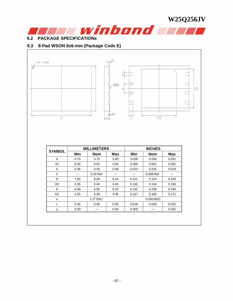
W25Q256JV
- 85 -
9.2 PACKAGE SPECIFICATIONs
9.3 8-Pad WSON 8x6-mm (Package Code E)
SYMBOL MILLIMETERS INCHES
Min Nom Max Min Nom Max
A 0.70 0.75 0.80 0.028 0.030 0.031
A1 0.00 0.02 0.05 0.000 0.001 0.002
b 0.35 0.40 0.48 0.014 0.016 0.019
C --- 0.20 Ref. --- --- 0.008 Ref. ---
D 7.90 8.00 8.10 0.311 0.315 0.319
D2 3.35 3.40 3.45 0.132 0.134 0.136
E 5.90 6.00 6.10 0.232 0.236 0.240
E2 4.25 4.30 4.35 0.167 0.169 0.171
e 1.27 BSC 0.050 BSC
L 0.45 0.50 0.55 0.018 0.020 0.022
y 0.00 --- 0.05 0.000 --- 0.002
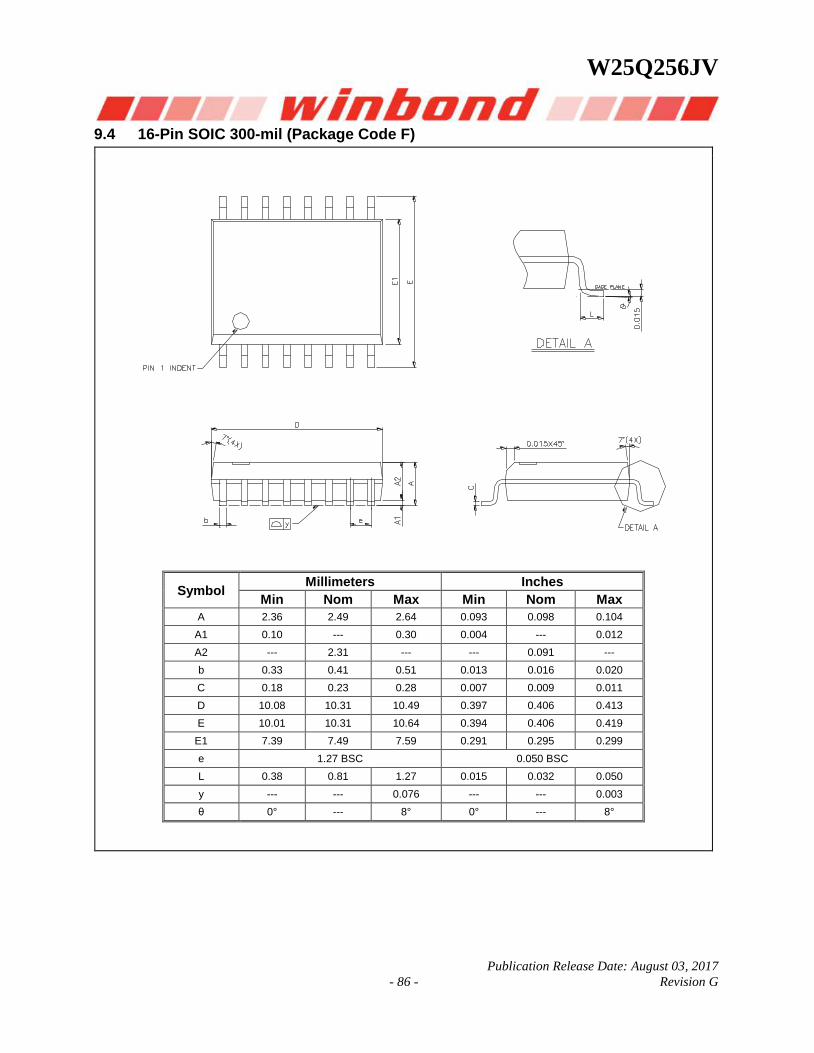
W25Q256JV
Publication Release Date: August 03, 2017
- 86 - Revision G
9.4 16-Pin SOIC 300-mil (Package Code F)
Symbol Millimeters Inches
Min Nom Max Min Nom Max
A 2.36 2.49 2.64 0.093 0.098 0.104
A1 0.10 --- 0.30 0.004 --- 0.012
A2 --- 2.31 --- --- 0.091 ---
b 0.33 0.41 0.51 0.013 0.016 0.020
C 0.18 0.23 0.28 0.007 0.009 0.011
D 10.08 10.31 10.49 0.397 0.406 0.413
E 10.01 10.31 10.64 0.394 0.406 0.419
E1 7.39 7.49 7.59 0.291 0.295 0.299
e 1.27 BSC 0.050 BSC
L 0.38 0.81 1.27 0.015 0.032 0.050
y --- --- 0.076 --- --- 0.003
θ 0° --- 8° 0° --- 8°
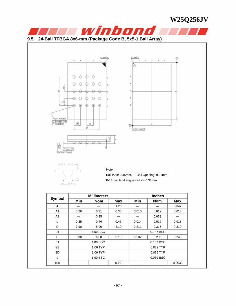
W25Q256JV
- 87 -
9.5 24-Ball TFBGA 8x6-mm (Package Code B, 5x5-1 Ball Array)
Symbol Millimeters Inches
Min Nom Max Min Nom Max
A --- --- 1.20 --- --- 0.047
A1 0.26 0.31 0.36 0.010 0.012 0.014
A2 --- 0.85 --- --- 0.033 ---
b 0.35 0.40 0.45 0.014 0.016 0.018
D 7.90 8.00 8.10 0.311 0.315 0.319
D1 4.00 BSC 0.157 BSC
E 5.90 6.00 6.10 0.232 0.236 0.240
E1 4.00 BSC 0.157 BSC
SE 1.00 TYP 0.039 TYP
SD 1.00 TYP 0.039 TYP
e 1.00 BSC 0.039 BSC
ccc --- --- 0.10 --- --- 0.0039
Note:
Ball land: 0.45mm. Ball Opening: 0.35mm
PCB ball land suggested <= 0.35mm
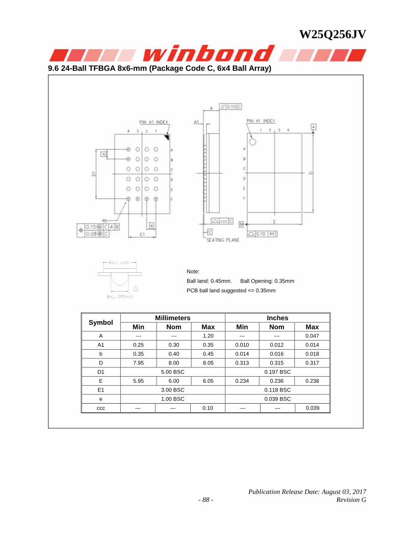
W25Q256JV
Publication Release Date: August 03, 2017
- 88 - Revision G
9.6 24-Ball TFBGA 8x6-mm (Package Code C, 6x4 Ball Array)
Symbol Millimeters Inches
Min Nom Max Min Nom Max
A --- --- 1.20 --- --- 0.047
A1 0.25 0.30 0.35 0.010 0.012 0.014
b 0.35 0.40 0.45 0.014 0.016 0.018
D 7.95 8.00 8.05 0.313 0.315 0.317
D1 5.00 BSC 0.197 BSC
E 5.95 6.00 6.05 0.234 0.236 0.238
E1 3.00 BSC 0.118 BSC
e 1.00 BSC 0.039 BSC
ccc --- --- 0.10 --- --- 0.039
Note:
Ball land: 0.45mm. Ball Opening: 0.35mm
PCB ball land suggested <= 0.35mm
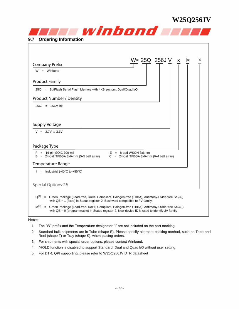
W25Q256JV
- 89 -
9.7 Ordering Information
Notes:
1. The “W” prefix and the Temperature designator “I” are not included on the part marking.
2. Standard bulk shipments are in Tube (shape E). Please specify alternate packing method, such as Tape and Reel (shape T) or Tray (shape S), when placing orders.
3. For shipments with special order options, please contact Winbond.
4. /HOLD function is disabled to support Standard, Dual and Quad I/O without user setting.
5. For DTR, QPI supporting, please refer to W25Q256JV DTR datasheet
W(1) 25Q 256J V x I(1)
W = Winbond
25Q = SpiFlash Serial Flash Memory with 4KB sectors, Dual/Quad I/O
256J = 256M-bit
V = 2.7V to 3.6V
F = 16-pin SOIC 300-mil E = 8-pad WSON 8x6mm B = 24-ball TFBGA 8x6-mm (5x5 ball array) C = 24-ball TFBGA 8x6-mm (6x4 ball array)
I = Industrial (-40°C to +85°C)
(2,3)
Q(4) = Green Package (Lead-free, RoHS Compliant, Halogen-free (TBBA), Antimony-Oxide-free Sb2O3)
with QE = 1 (fixed) in Status register-2. Backward compatible to FV family.
M(5) = Green Package (Lead-free, RoHS Compliant, Halogen-free (TBBA), Antimony-Oxide-free Sb2O3)
with QE = 0 (programmable) in Status register-2. New device ID is used to identify JV family
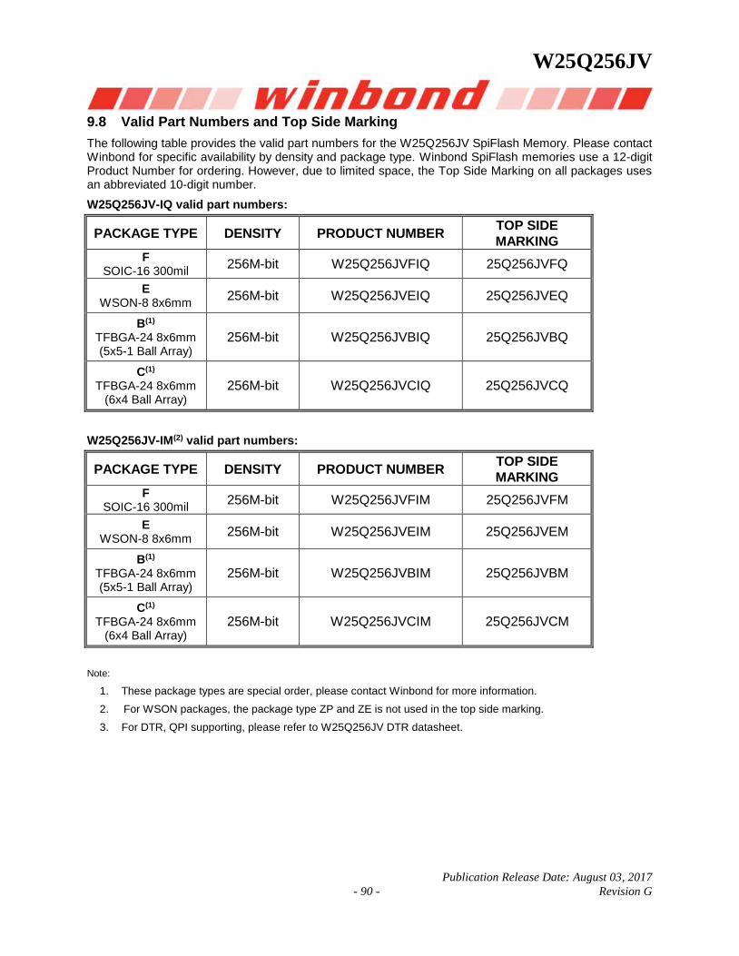
W25Q256JV
Publication Release Date: August 03, 2017
- 90 - Revision G
9.8 Valid Part Numbers and Top Side Marking
The following table provides the valid part numbers for the W25Q256JV SpiFlash Memory. Please contact Winbond for specific availability by density and package type. Winbond SpiFlash memories use a 12-digit Product Number for ordering. However, due to limited space, the Top Side Marking on all packages uses an abbreviated 10-digit number.
W25Q256JV-IQ valid part numbers:
PACKAGE TYPE DENSITY PRODUCT NUMBER TOP SIDE
MARKING F
SOIC-16 300mil 256M-bit W25Q256JVFIQ 25Q256JVFQ
E WSON-8 8x6mm
256M-bit W25Q256JVEIQ 25Q256JVEQ
B(1) TFBGA-24 8x6mm (5x5-1 Ball Array)
256M-bit W25Q256JVBIQ 25Q256JVBQ
C(1) TFBGA-24 8x6mm
(6x4 Ball Array) 256M-bit W25Q256JVCIQ 25Q256JVCQ
W25Q256JV-IM(2) valid part numbers:
PACKAGE TYPE DENSITY PRODUCT NUMBER TOP SIDE
MARKING F
SOIC-16 300mil 256M-bit W25Q256JVFIM 25Q256JVFM
E WSON-8 8x6mm
256M-bit W25Q256JVEIM 25Q256JVEM
B(1) TFBGA-24 8x6mm (5x5-1 Ball Array)
256M-bit W25Q256JVBIM 25Q256JVBM
C(1) TFBGA-24 8x6mm
(6x4 Ball Array) 256M-bit W25Q256JVCIM 25Q256JVCM
Note:
1. These package types are special order, please contact Winbond for more information.
2. For WSON packages, the package type ZP and ZE is not used in the top side marking.
3. For DTR, QPI supporting, please refer to W25Q256JV DTR datasheet.
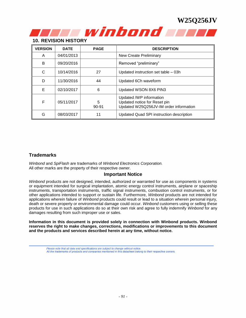
W25Q256JV
- 91 -
10. REVISION HISTORY
VERSION DATE PAGE DESCRIPTION
A 04/01/2013 New Create Preliminary
B 09/20/2016 Removed “preliminary”
C 10/14/2016 27 Updated instruction set table – 03h
D 11/30/2016 44 Updated 6Ch waveform
E 02/10/2017 6 Updated WSON 8X6 PIN3
F 05/11/2017 5
90-91
Updated /WP information Updated notice for Reset pin Updated W25Q256JV-IM order information
G 08/03/2017 11 Updated Quad SPI instruction description
Trademarks
Winbond and SpiFlash are trademarks of Winbond Electronics Corporation. All other marks are the property of their respective owner.
Important Notice
Winbond products are not designed, intended, authorized or warranted for use as components in systems or equipment intended for surgical implantation, atomic energy control instruments, airplane or spaceship instruments, transportation instruments, traffic signal instruments, combustion control instruments, or for other applications intended to support or sustain life. Furthermore, Winbond products are not intended for applications wherein failure of Winbond products could result or lead to a situation wherein personal injury, death or severe property or environmental damage could occur. Winbond customers using or selling these products for use in such applications do so at their own risk and agree to fully indemnify Winbond for any damages resulting from such improper use or sales.
Information in this document is provided solely in connection with Winbond products. Winbond reserves the right to make changes, corrections, modifications or improvements to this document and the products and services described herein at any time, without notice.