Embed Size (px)
Citation preview
1
2
3
6
5
4
VDD
IN-
IN+
VREF
OUTH
OUTL
UCC27611
R1
R2
Q1
IN+
D1
C1
+
VOUT
VSOURCE
L1
C3
VREF4.5 V to 18 V
Non-Inverting Input Inverting Input
C2
VDD
1
2
3
6
5
4
VDD
IN-
IN+
VREF
OUTH
OUTL
UCC27611
R1
R2
Q1
VREF
D1
C1
+
VOUT
VSOURCE
L1
C3
VREF4.5 V to 18 V
C2
VDD
IN-
7
GND
7
GND
UCC27611
www.ti.com SLUSBA5B –DECEMBER 2012
4-A and 6-A High-Speed 5-V Drive, Optimized Single-Gate DriverCheck for Samples: UCC27611
1FEATURES APPLICATIONS• Enhancement Mode Gallium Nitride FETs • Switch-Mode Power Supplies
(eGANFETs) • DC-to-DC Converters• 4.0-V to 18-V Single Supply Range VDD Range • Synchronous Rectification• Drive Voltage VREF Regulated to 5 V • Solar Inverters, Motor Control, UPS• 4-A Peak Source and 6-A Peak Sink Drive • Envelope Tracking Power Supplies
Current• 1-Ω and 0.35-Ω Pull-Up and Pull-Down DESCRIPTION
Resistance (maximize high slew-rate dV and dt The UCC27611 is a single-channel, high-speed, gateimmunity) driver optimized for 5-V drive, specifically addressing
enhancement mode GaN FETs. The drive voltage• Split Output Configuration (allows turn-on andVREF is precisely controlled by internal linearoff optimization for individual FETs)regulator to 5 V. The UCC27611 offers asymmetrical
• Fast Propagation Delays (14-ns typical) rail-to-rail peak current drive capability with 4-A• Fast Rise and Fall Times (9-ns and 4-ns source and 6-A sink. Split output configuration allows
individual turn-on and off time optimization dependingtypical)on FET. Package and pinout with minimum parasitic• TTL and CMOS Compatible Inputsinductances reduce the rise and fall time and limit the(independent of supply voltage allow easyringing. Additionally, the short propagation delay with
interface to digital and analog controllers) minimized tolerances and variations allows efficient• Dual Input Design offering Drive Flexibility operation at high frequencies. The 2-Ω and 0.3-Ω
(both inverting and non-inverting pull-up and pull-down resistance boosts immunity tohard switching with high slew rate dV and dt.configurations)
• Output Held Low when Inputs are Floating The independence from VDD input signal thresholdsensure TTL and CMOS low-voltage logic• VDD Under Voltage Lockout (UVLO)compatibility. For safety reason when the input pins• Optimized Pinout Compatible with eGANFETare in a floating condition, the internal input pull-upFootprint for Easy Layout and down resistors hold the output LOW. Internal
• 2 mm x 2 mm WSON-6 Package with Exposed circuitry on VREF pin provides an under voltageThermal and Ground Pad, (minimized parasitic lockout function that holds output LOW until VREF
supply voltage is within operating range. UCC27611inductances to reduce gate ringing)is offered in a small 2 mm x 2 mm WSON-6 package• Operating Temperature Range of -40°C to(DRV) with exposed thermal and ground pad which140°Cimproves the package power handling capability. TheUCC27611 operates over wide temperature rangefrom -40°C to 140°C.
Typical Application Diagram
1
Please be aware that an important notice concerning availability, standard warranty, and use in critical applications ofTexas Instruments semiconductor products and disclaimers thereto appears at the end of this data sheet.
PRODUCTION DATA information is current as of publication date. Copyright © 2012, Texas Instruments IncorporatedProducts conform to specifications per the terms of the TexasInstruments standard warranty. Production processing does notnecessarily include testing of all parameters.
UCC27611
SLUSBA5B –DECEMBER 2012 www.ti.com
This integrated circuit can be damaged by ESD. Texas Instruments recommends that all integrated circuits be handled withappropriate precautions. Failure to observe proper handling and installation procedures can cause damage.
ESD damage can range from subtle performance degradation to complete device failure. Precision integrated circuits may be moresusceptible to damage because very small parametric changes could cause the device not to meet its published specifications.
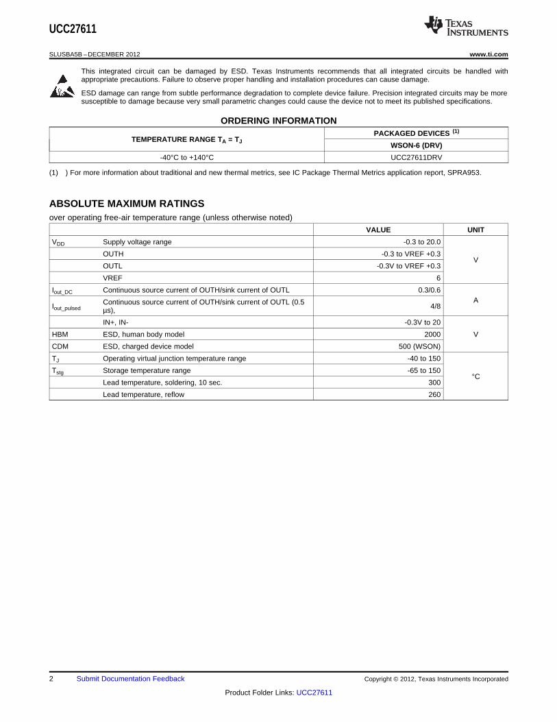
ORDERING INFORMATIONPACKAGED DEVICES (1)
TEMPERATURE RANGE TA = TJWSON-6 (DRV)
-40°C to +140°C UCC27611DRV
(1) ) For more information about traditional and new thermal metrics, see IC Package Thermal Metrics application report, SPRA953.
ABSOLUTE MAXIMUM RATINGSover operating free-air temperature range (unless otherwise noted)
VALUE UNIT
VDD Supply voltage range -0.3 to 20.0
OUTH -0.3 to VREF +0.3V
OUTL -0.3V to VREF +0.3
VREF 6
Iout_DC Continuous source current of OUTH/sink current of OUTL 0.3/0.6AContinuous source current of OUTH/sink current of OUTL (0.5Iout_pulsed 4/8µs),
IN+, IN- -0.3V to 20
HBM ESD, human body model 2000 V
CDM ESD, charged device model 500 (WSON)
TJ Operating virtual junction temperature range -40 to 150
Tstg Storage temperature range -65 to 150°C
Lead temperature, soldering, 10 sec. 300
Lead temperature, reflow 260
2 Submit Documentation Feedback Copyright © 2012, Texas Instruments Incorporated
Product Folder Links: UCC27611
UCC27611
www.ti.com SLUSBA5B –DECEMBER 2012
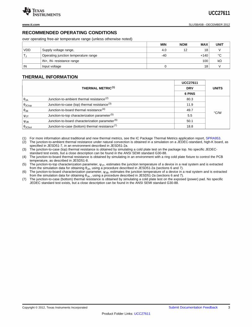
RECOMMENDED OPERATING CONDITIONSover operating free-air temperature range (unless otherwise noted)
MIN NOM MAX UNIT
VDD Supply voltage range, 4.0 12 18 V
TJ Operating junction temperature range -40 +140 °C
IN+, IN- resistance range 100 kΩIN Input voltage 0 18 V
THERMAL INFORMATIONUCC27611
THERMAL METRIC (1) DRV UNITS
6 PINS
θJA Junction-to-ambient thermal resistance (2) 80.3
θJCtop Junction-to-case (top) thermal resistance (3) 11.9
θJB Junction-to-board thermal resistance (4) 49.7°C/W
ψJT Junction-to-top characterization parameter (5) 5.5
ψJB Junction-to-board characterization parameter (6) 50.1
θJCbot Junction-to-case (bottom) thermal resistance (7) 18.8
(1) For more information about traditional and new thermal metrics, see the IC Package Thermal Metrics application report, SPRA953.(2) The junction-to-ambient thermal resistance under natural convection is obtained in a simulation on a JEDEC-standard, high-K board, as
specified in JESD51-7, in an environment described in JESD51-2a.(3) The junction-to-case (top) thermal resistance is obtained by simulating a cold plate test on the package top. No specific JEDEC-
standard test exists, but a close description can be found in the ANSI SEMI standard G30-88.(4) The junction-to-board thermal resistance is obtained by simulating in an environment with a ring cold plate fixture to control the PCB
temperature, as described in JESD51-8.(5) The junction-to-top characterization parameter, ψJT, estimates the junction temperature of a device in a real system and is extracted
from the simulation data for obtaining θJA, using a procedure described in JESD51-2a (sections 6 and 7).(6) The junction-to-board characterization parameter, ψJB, estimates the junction temperature of a device in a real system and is extracted
from the simulation data for obtaining θJA , using a procedure described in JESD51-2a (sections 6 and 7).(7) The junction-to-case (bottom) thermal resistance is obtained by simulating a cold plate test on the exposed (power) pad. No specific
JEDEC standard test exists, but a close description can be found in the ANSI SEMI standard G30-88.Spacer
Copyright © 2012, Texas Instruments Incorporated Submit Documentation Feedback 3
Product Folder Links: UCC27611
UCC27611
SLUSBA5B –DECEMBER 2012 www.ti.com
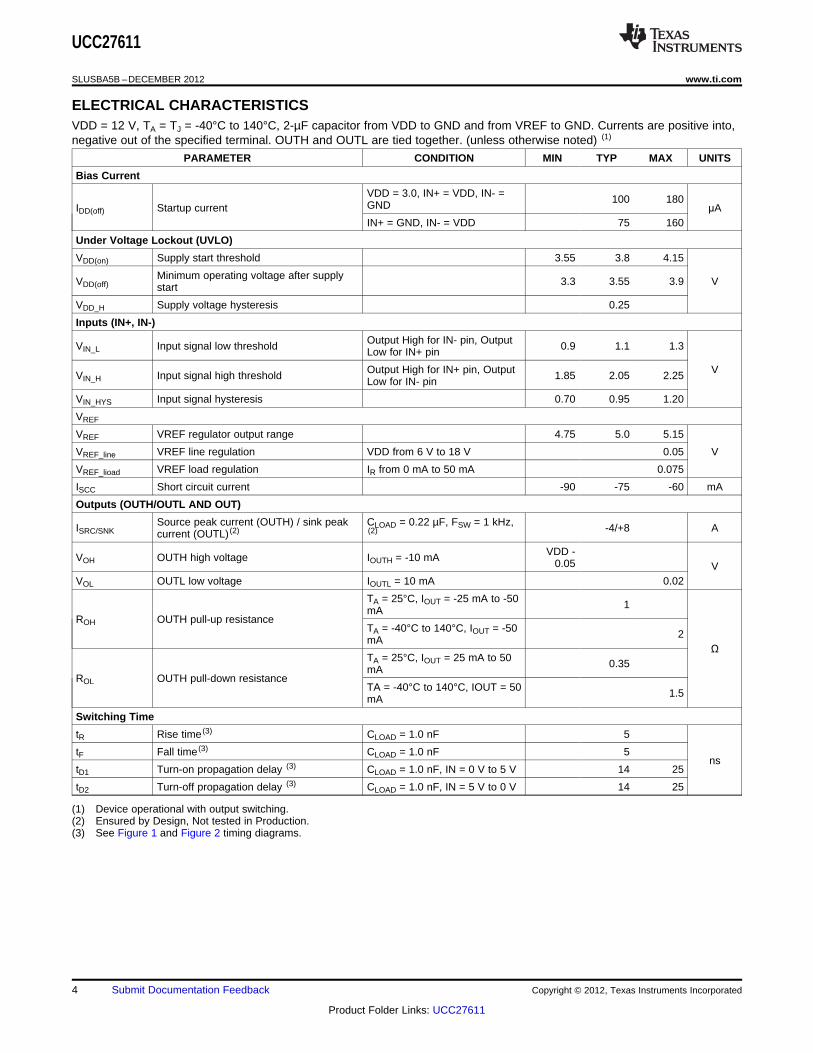
ELECTRICAL CHARACTERISTICSVDD = 12 V, TA = TJ = -40°C to 140°C, 2-µF capacitor from VDD to GND and from VREF to GND. Currents are positive into,negative out of the specified terminal. OUTH and OUTL are tied together. (unless otherwise noted) (1)
PARAMETER CONDITION MIN TYP MAX UNITS
Bias Current
VDD = 3.0, IN+ = VDD, IN- = 100 180GNDIDD(off) Startup current μAIN+ = GND, IN- = VDD 75 160
Under Voltage Lockout (UVLO)
VDD(on) Supply start threshold 3.55 3.8 4.15
Minimum operating voltage after supplyVDD(off) 3.3 3.55 3.9 Vstart
VDD_H Supply voltage hysteresis 0.25
Inputs (IN+, IN-)
Output High for IN- pin, OutputVIN_L Input signal low threshold 0.9 1.1 1.3Low for IN+ pin
Output High for IN+ pin, Output VVIN_H Input signal high threshold 1.85 2.05 2.25Low for IN- pin
VIN_HYS Input signal hysteresis 0.70 0.95 1.20
VREF
VREF VREF regulator output range 4.75 5.0 5.15
VREF_line VREF line regulation VDD from 6 V to 18 V 0.05 V
VREF_lioad VREF load regulation IR from 0 mA to 50 mA 0.075
ISCC Short circuit current -90 -75 -60 mA
Outputs (OUTH/OUTL AND OUT)
Source peak current (OUTH) / sink peak CLOAD = 0.22 µF, FSW = 1 kHz,ISRC/SNK -4/+8 Acurrent (OUTL) (2) (2)
VDD -VOH OUTH high voltage IOUTH = -10 mA 0.05 VVOL OUTL low voltage IOUTL = 10 mA 0.02
TA = 25°C, IOUT = -25 mA to -50 1mAROH OUTH pull-up resistance
TA = -40°C to 140°C, IOUT = -50 2mAΩ
TA = 25°C, IOUT = 25 mA to 50 0.35mAROL OUTH pull-down resistance
TA = -40°C to 140°C, IOUT = 50 1.5mA
Switching Time
tR Rise time (3) CLOAD = 1.0 nF 5
tF Fall time (3) CLOAD = 1.0 nF 5ns
tD1 Turn-on propagation delay (3) CLOAD = 1.0 nF, IN = 0 V to 5 V 14 25
tD2 Turn-off propagation delay (3) CLOAD = 1.0 nF, IN = 5 V to 0 V 14 25
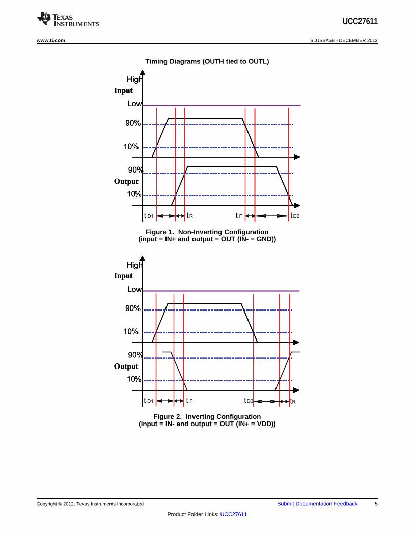
(1) Device operational with output switching.(2) Ensured by Design, Not tested in Production.(3) See Figure 1 and Figure 2 timing diagrams.
4 Submit Documentation Feedback Copyright © 2012, Texas Instruments Incorporated
Product Folder Links: UCC27611
Low
90%
10%
90%
10%
Output
High
Input
Low
90%
10%
90%
10%
Output
t D1
High
Input
High
Input
tD2t tF R
Low
90%
10%
90%
10%
Output
High
Input
Low
90%
10%
90%
10%
Output
t D1
High
Input
High
Input
tD2t tR F
UCC27611
www.ti.com SLUSBA5B –DECEMBER 2012
Timing Diagrams (OUTH tied to OUTL)
Figure 1. Non-Inverting Configuration(input = IN+ and output = OUT (IN- = GND))
Figure 2. Inverting Configuration(input = IN- and output = OUT (IN+ = VDD))
Copyright © 2012, Texas Instruments Incorporated Submit Documentation Feedback 5
Product Folder Links: UCC27611
UCC27611
SLUSBA5B –DECEMBER 2012 www.ti.com
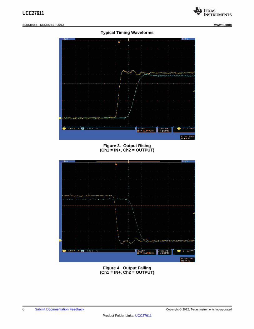
Typical Timing Waveforms
Figure 3. Output Rising(Ch1 = IN+, Ch2 = OUTPUT)
Figure 4. Output Falling(Ch1 = IN+, Ch2 = OUTPUT)
6 Submit Documentation Feedback Copyright © 2012, Texas Instruments Incorporated
Product Folder Links: UCC27611
4
5
61
2
3
VDD
IN+
VREF
GND PAD
Pin 7IN-
OUTL
OUTH
(Top view)
3
2
1
6
5
4
VDD
UVLO
VREF
VREF
VREF
OUTH
GND
IN+
IN-
VDD
7
OUTLLDO
VREFVDD
UCC27611
www.ti.com SLUSBA5B –DECEMBER 2012
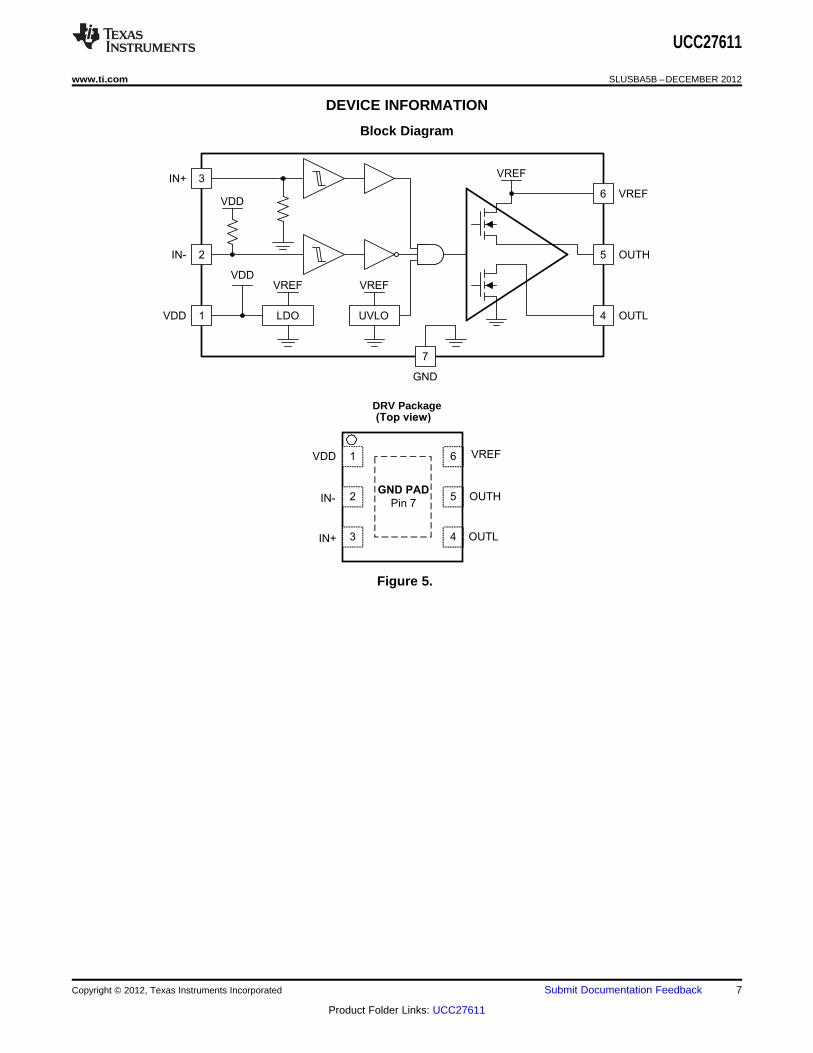
DEVICE INFORMATION
Block Diagram
DRV Package
Figure 5.
Copyright © 2012, Texas Instruments Incorporated Submit Documentation Feedback 7
Product Folder Links: UCC27611
UCC27611
SLUSBA5B –DECEMBER 2012 www.ti.com
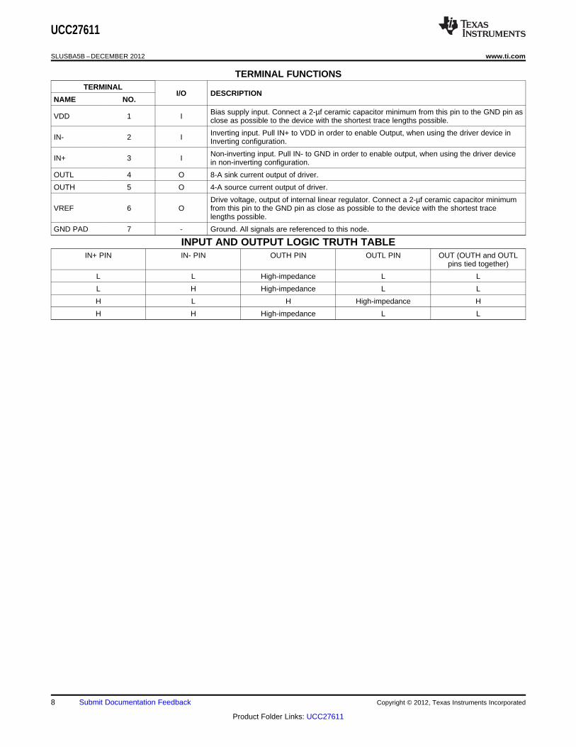
TERMINAL FUNCTIONSTERMINAL
I/O DESCRIPTIONNAME NO.
Bias supply input. Connect a 2-µf ceramic capacitor minimum from this pin to the GND pin asVDD 1 I close as possible to the device with the shortest trace lengths possible.
Inverting input. Pull IN+ to VDD in order to enable Output, when using the driver device inIN- 2 I Inverting configuration.
Non-inverting input. Pull IN- to GND in order to enable output, when using the driver deviceIN+ 3 I in non-inverting configuration.
OUTL 4 O 8-A sink current output of driver.
OUTH 5 O 4-A source current output of driver.
Drive voltage, output of internal linear regulator. Connect a 2-µf ceramic capacitor minimumVREF 6 O from this pin to the GND pin as close as possible to the device with the shortest trace
lengths possible.
GND PAD 7 - Ground. All signals are referenced to this node.
INPUT AND OUTPUT LOGIC TRUTH TABLEIN+ PIN IN- PIN OUTH PIN OUTL PIN OUT (OUTH and OUTL
pins tied together)
L L High-impedance L L
L H High-impedance L L
H L H High-impedance H
H H High-impedance L L
8 Submit Documentation Feedback Copyright © 2012, Texas Instruments Incorporated
Product Folder Links: UCC27611
5
5.2
5.4
5.6
5.8
6
−50 0 50 100 150Temperature (°C)
Ris
e T
ime
(ns)
VDD = 12 VCLoad = 1.8nF
G001
5
5.2
5.4
5.6
5.8
6
−50 0 50 100 150Temperature (°C)
Fal
l Tim
e (n
s)
VDD = 12 VCLoad = 1.8nF
G001
10
12
14
16
18
20
−50 0 50 100 150Temperature (°C)
IN−
Pro
paga
tion
Del
ay (
ns)
Turn−OnTurn−Off
VDD = 12 V
G001
0.2
0.3
0.4
−50 0 50 100 150Temperature (°C)
UV
LO H
yste
rsis
(V
)
UVLO Hysterisis
G001
4.8
4.9
5
−50 0 50 100 150Temperature (°C)
VR
EF
(V
)
G001
8
10
12
14
16
18
−50 0 50 100 150Temperature (°C)
IN+
Pro
paga
tion
Del
ay (
ns)
Turn−OnTurn−Off
VDD = 12 V
G001
UCC27611
www.ti.com SLUSBA5B –DECEMBER 2012
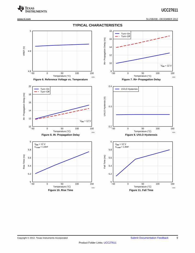
TYPICAL CHARACTERISTICS
Figure 6. Reference Voltage vs. Temperature Figure 7. IN+ Propagation Delay
Figure 8. IN- Propagation Delay Figure 9. UVLO Hysteresis
Figure 10. Rise Time Figure 11. Fall Time
Copyright © 2012, Texas Instruments Incorporated Submit Documentation Feedback 9
Product Folder Links: UCC27611
UCC27611
SLUSBA5B –DECEMBER 2012 www.ti.com
APPLICATION INFORMATION
Introduction
High-current gate driver devices are required in switching power applications for a variety of reasons. In order toeffect fast switching of power devices and reduce associated switching power losses, a powerful gate driver canbe employed between the PWM output of controllers and the gates of the power semiconductor devices. Further,gate drivers are indispensable when sometimes it is just not feasible to have the PWM controller directly drivethe gates of the switching devices. With advent of digital power, this situation will be often encountered since thePWM signal from the digital controller is often a 3.3-V logic signal which is not capable of effectively turning on apower switch. A level shifting circuitry is needed to boost the 3.3-V signal to the gate-drive voltage (such as 12 V)in order to fully turn on the power device and minimize conduction losses. Traditional buffer drive circuits basedon NPN and PNP bipolar transistors in totem-pole arrangement, being emitter follower configurations, proveinadequate with digital power since they lack level-shifting capability. Gate drivers effectively combine both thelevel-shifting and buffer-drive functions. Gate drivers also find other needs such as minimizing the effect of high-frequency switching noise by locating the high-current driver physically close to the power switch, driving gate-drive transformers and controlling floating power-device gates, reducing power dissipation and thermal stress incontrollers by moving gate charge power losses into itself. Finally, emerging wide band-gap power devicetechnologies such as GaN based switches, which are capable of supporting very high switching frequencyoperation, are driving very special requirements in terms of gate drive capability. These requirements includeoperation at low VDD voltages (5 V or lower), low propagation delays and availability in compact, low-inductancepackages with good thermal capability. In summary gate-driver devices are extremely important components inswitching power combining benefits of high-performance, low cost, component count and board space reductionand simplified system design.
VDD and Undervoltage Lockout
The UCC27611 devices have internal Under Voltage LockOut (UVLO) protection feature on the VDD pin supplycircuit blocks. Whenever the driver is in UVLO condition (i.e. when VDD voltage less than VON during power upand when VDD voltage is less than VOFF during power down), this circuit holds all outputs LOW, regardless ofthe status of the inputs. The UVLO is typically 3.8 V with 250-mV typical hysteresis. This hysteresis helpsprevent chatter when low VDD supply voltages have noise from the power supply and also when there aredroops in the VDD bias voltage when the system commences switching and there is a sudden increase in IDD.The capability to operate at low voltage levels such as below 5 V, along with best-in-class switchingcharacteristics, is especially suited for driving emerging GaN wide bandgap power semiconductor devices.
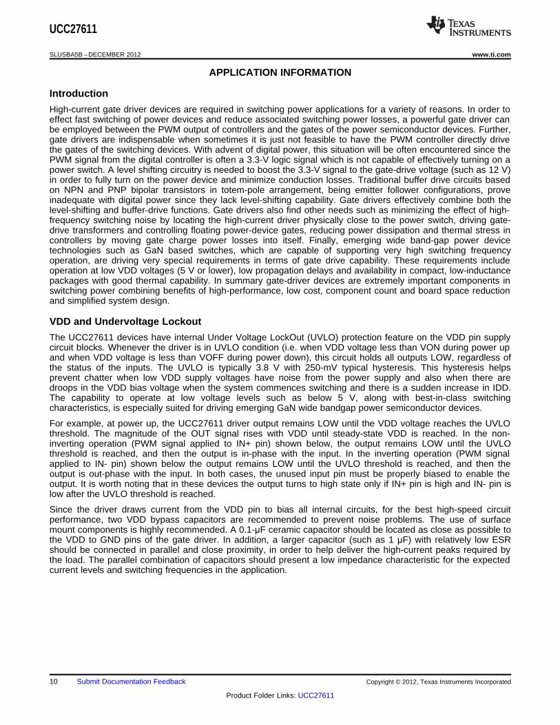
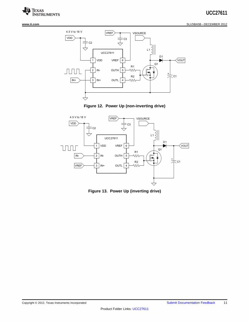
For example, at power up, the UCC27611 driver output remains LOW until the VDD voltage reaches the UVLOthreshold. The magnitude of the OUT signal rises with VDD until steady-state VDD is reached. In the non-inverting operation (PWM signal applied to IN+ pin) shown below, the output remains LOW until the UVLOthreshold is reached, and then the output is in-phase with the input. In the inverting operation (PWM signalapplied to IN- pin) shown below the output remains LOW until the UVLO threshold is reached, and then theoutput is out-phase with the input. In both cases, the unused input pin must be properly biased to enable theoutput. It is worth noting that in these devices the output turns to high state only if IN+ pin is high and IN- pin islow after the UVLO threshold is reached.
Since the driver draws current from the VDD pin to bias all internal circuits, for the best high-speed circuitperformance, two VDD bypass capacitors are recommended to prevent noise problems. The use of surfacemount components is highly recommended. A 0.1-μF ceramic capacitor should be located as close as possible tothe VDD to GND pins of the gate driver. In addition, a larger capacitor (such as 1 μF) with relatively low ESRshould be connected in parallel and close proximity, in order to help deliver the high-current peaks required bythe load. The parallel combination of capacitors should present a low impedance characteristic for the expectedcurrent levels and switching frequencies in the application.
10 Submit Documentation Feedback Copyright © 2012, Texas Instruments Incorporated
Product Folder Links: UCC27611
1
2
3
6
5
4
VDD
IN-
IN+
VREF
OUTH
OUTL
UCC27611
R1
R2
Q1
VREF
D1
C1
+
VOUT
VSOURCE
L1
C3
VREF4.5 V to 18 V
C2
VDD
IN-
1
2
3
6
5
4
VDD
IN-
IN+
VREF
OUTH
OUTL
UCC27611
R1
R2
Q1
IN+
D1
C1
+
VOUT
VSOURCE
L1
C3
VREF4.5 V to 18 V
C2
VDD
UCC27611
www.ti.com SLUSBA5B –DECEMBER 2012
Figure 12. Power Up (non-inverting drive)
Figure 13. Power Up (inverting drive)
Copyright © 2012, Texas Instruments Incorporated Submit Documentation Feedback 11
Product Folder Links: UCC27611
UCC27611
SLUSBA5B –DECEMBER 2012 www.ti.com
Operating Supply Current
The UCC27611 feature very low quiescent IDD current. The total supply current is the sum of the quiescent IDDcurrent, the average IOUT current due to switching and finally any current related to pull-up resistors on theunused input pin. For example when the inverting input pin is pulled low additional current is drawn from VDDsupply through the pull-up resistors (refer to DEVICE INFORMATION for the device Block Diagram). Knowingthe operating frequency (fSW) and the MOSFET gate (QG) charge at the drive voltage being used, the averageIOUT current can be calculated as product of QG and fSW.
Input Stage
The input pins of the UCC27611 is based on a TTL and CMOS compatible input threshold logic that isindependent of the VDD supply voltage. With typical high threshold = 1.95 V and typical low threshold = 1.3 V,the logic level thresholds can be conveniently driven with PWM control signals derived from 3.3-V and 5-V digitalpower controllers. Wider hysteresis (typ 1 V) offers enhanced noise immunity compared to traditional TTL logicimplementations, where the hysteresis is typically less than 0.5 V. These devices also feature tight control of theinput pin threshold voltage levels which eases system design considerations and ensures stable operation acrosstemperature. The very low input capacitance on these pins reduces loading and increases switching speed.
The device features an important safety function wherein, whenever any of the input pins are in a floatingcondition, the output of the respective channel is held in the low state. This is achieved using VDD pull-upresistors on all the inverting inputs (IN- pin) or GND pull-down resistors on all the non-inverting input pins (IN+pin), (refer to DEVICE INFORMATION for the device Block Diagram).
The device also features a dual input configuration with two input pins available to control the state of the output.The user has the flexibility to drive the device using either a non-inverting input pin (IN+) or an inverting input pin(IN-). The state of the output pin is dependent on the bias on both the IN+ and IN- pins. Refer to INPUT ANDOUTPUT LOGIC TRUTH TABLE input and output logic truth table and the Typical Application Diagram, foradditional clarification.
Once an input pin has been chosen for PWM drive, the other input pin (the unused input pin) must be properlybiased in order to enable the output. As mentioned earlier, the unused input pin cannot remain in a floatingcondition because whenever any input pin is left in a floating condition the output is disabled for safety purposes.Alternatively, the unused input pin can effectively be used to implement an enable and disable function, asexplained below.• In order to drive the device in a non-inverting configuration, apply the PWM control input signal to IN+ pin. In
this case, the unused input pin, IN-, must be biased low (tied to GND) in order to enable the output.– Alternately, the IN- pin can be used to implement the enable and disable function using an external logic
signal. OUT is disabled when IN- is biased high and OUT is enabled when IN- is biased low.• In order to drive the device in an inverting configuration, apply the PWM control input signal to IN- pin. In this
case, the unused input pin, IN+, must be biased high (eg. tied to VDD) in order to enable the output.– Alternately, the IN+ pin can be used to implement the enable and disable function using an external logic
signal. OUT is disabled when IN+ is biased low and OUT is enabled when IN+ is biased high.• Finally, it is worth noting that the output pin can be driven into a high state ONLY when IN+ pin is biased high
and IN- input is biased low.
The input stage of the driver should preferably be driven by a signal with a short rise or fall time. Caution must beexercised whenever the driver is used with slowly varying input signals, especially in situations where the deviceis located in a mechanical socket or PCB layout is not optimal:• High dI and dt current from the driver output coupled with board layout parasitic can cause ground bounce.
Since the device features just one GND pin which may be referenced to the power ground, this may modifythe differential voltage between input pins and GND and trigger an unintended change of output state.Because of fast 13-ns propagation delay, this can ultimately result in high-frequency oscillations, whichincreases power dissipation and poses risk of damage.
• 1-V input threshold hysteresis boosts noise immunity compared to most other industry standard drivers.• In the worst case, when a slow input signal is used and PCB layout is not optimal, it may be necessary to add
a small capacitor (1 nF) between input pin and ground very close to the driver device. This helps to convertthe differential mode noise with respect to the input logic circuitry into common mode noise and avoidunintended change of output state.
12 Submit Documentation Feedback Copyright © 2012, Texas Instruments Incorporated
Product Folder Links: UCC27611
VREF
ROH
ROL
Gate
Voltage
Boost
Narrow Pulse at
each Turn On
Anti Shoot -
Through
Circuitry
Input Signal
RNMOS, Pull Up
OUTL
OUTH
UCC27611
www.ti.com SLUSBA5B –DECEMBER 2012
Enable Function
As mentioned earlier, an enable and disable function can be easily implemented in UCC27611 using the unusedinput pin. When IN+ is pulled down to GND or IN- is pulled down to VDD, the output is disabled. Thus IN+ pincan be used like an enable pin that is based on active high logic, while IN- can be used like an enable pin that isbased on active low logic.
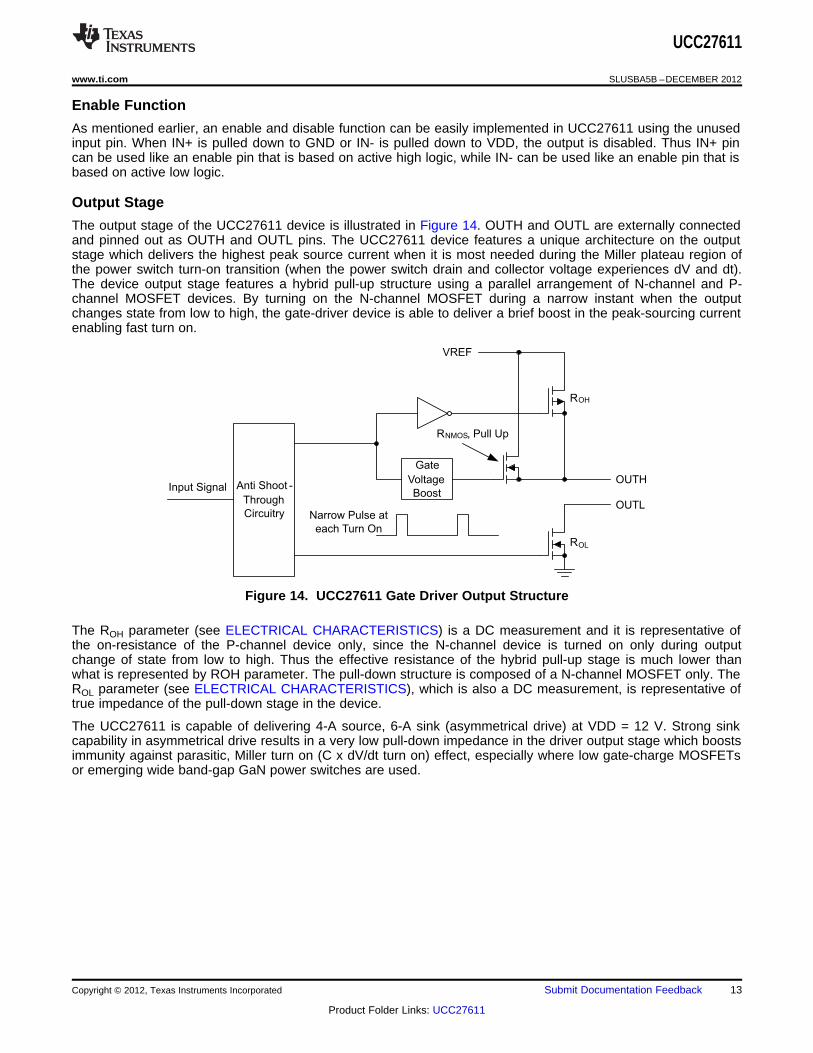
Output Stage
The output stage of the UCC27611 device is illustrated in Figure 14. OUTH and OUTL are externally connectedand pinned out as OUTH and OUTL pins. The UCC27611 device features a unique architecture on the outputstage which delivers the highest peak source current when it is most needed during the Miller plateau region ofthe power switch turn-on transition (when the power switch drain and collector voltage experiences dV and dt).The device output stage features a hybrid pull-up structure using a parallel arrangement of N-channel and P-channel MOSFET devices. By turning on the N-channel MOSFET during a narrow instant when the outputchanges state from low to high, the gate-driver device is able to deliver a brief boost in the peak-sourcing currentenabling fast turn on.
Figure 14. UCC27611 Gate Driver Output Structure
The ROH parameter (see ELECTRICAL CHARACTERISTICS) is a DC measurement and it is representative ofthe on-resistance of the P-channel device only, since the N-channel device is turned on only during outputchange of state from low to high. Thus the effective resistance of the hybrid pull-up stage is much lower thanwhat is represented by ROH parameter. The pull-down structure is composed of a N-channel MOSFET only. TheROL parameter (see ELECTRICAL CHARACTERISTICS), which is also a DC measurement, is representative oftrue impedance of the pull-down stage in the device.
The UCC27611 is capable of delivering 4-A source, 6-A sink (asymmetrical drive) at VDD = 12 V. Strong sinkcapability in asymmetrical drive results in a very low pull-down impedance in the driver output stage which boostsimmunity against parasitic, Miller turn on (C x dV/dt turn on) effect, especially where low gate-charge MOSFETsor emerging wide band-gap GaN power switches are used.
Copyright © 2012, Texas Instruments Incorporated Submit Documentation Feedback 13
Product Folder Links: UCC27611

Gate Driver
ROL
RG
CGD
CGS
COSS
VDS VIN
ISNK
VIN
VTH
ON OFF
Miller Turn -On Spike in V GS
VDS of
MOSFET
VGS of
MOSFET
UCC27611
SLUSBA5B –DECEMBER 2012 www.ti.com
An example of a situation where Miller turn on is a concern is synchronous rectification (SR). In SR application,the dV and dt occurs on MOSFET drain when the MOSFET is already held in off state by the gate driver. Thecurrent discharging the CGD Miller capacitance during this dV and dt is shunted by the pull-down stage of thedriver. If the pull-down impedance is not low enough then a voltage spike can result in the VGS of the MOSFET,which can result in spurious turn on. This phenomenon is illustrated in Figure 15. UCC27611 offers a best-in-class, 0.35-Ω (typ) pull-down impedance boosting immunity against Miller turn on.
Figure 15. Low Pull-Down Impedance in UCC27611, 4-A and 6-A Asymmetrical Drive(output stage mitigates Miller turn-on effect)
The driver output voltage swings between VDD and GND providing rail-to-rail operation, thanks to the MOSoutput stage which delivers very low dropout. The presence of the MOSFET body diodes also offers lowimpedance to switching overshoots and undershoots. This means that in many cases, external Schottky diodeclamps may be eliminated. The outputs of these drivers are designed to withstand 500-mA reverse currentwithout either damage to the device or logic malfunction.
14 Submit Documentation Feedback Copyright © 2012, Texas Instruments Incorporated
Product Folder Links: UCC27611

( ) ( )OFF ON
SW g REF SWOFF GATE ON GATE
R RP Q V f
R R R R
æ ö= ´ ´ ´ç ÷ç ÷+ +è ø
2 2G LOAD REF SW g REF SWP C V f Q V f= ´ ´ = ´ ´
2G LOAD REF SWP C V f= ´ ´
2LOAD REF
1EG C V
2= ´ ´
DISS DC SWP P P´ +
UCC27611
www.ti.com SLUSBA5B –DECEMBER 2012
Power Dissipation
Power dissipation of the gate driver has two portions as shown in equation below:
(1)
The DC portion of the power dissipation is PDC = IQ x VDD where IQ is the quiescent current for the driver. Thequiescent current is the current consumed by the device to bias all internal circuits such as input stage, referencevoltage, logic circuits, protections etc and also any current associated with switching of internal devices when thedriver output changes state (such as charging and discharging of parasitic capacitances, parasitic shoot-throughetc). The UCC27611 features very low quiescent currents (less than 1 mA, refer ELECTRICALCHARACTERISTICS) and contains internal logic to eliminate any shoot-through in the output driver stage. Thusthe effect of the PDC on the total power dissipation within the gate driver can be safely assumed to be negligible.
The power dissipated in the gate-driver package during switching (PSW) depends on the following factors:• Gate charge required of the power device (usually a function of the drive voltage VG, which is very close to
input bias supply voltage VREF due to low VOH dropout).• Switching frequency.• Use of external gate resistors.
When a driver device is tested with a discrete, capacitive load it is a fairly simple matter to calculate the powerthat is required from the bias supply. The energy that must be transferred from the bias supply to charge thecapacitor is given by:
where• Where CLOAD is load capacitor and VDD is bias voltage feeding the driver. (2)
There is an equal amount of energy dissipated when the capacitor is charged. This leads to a total power lossgiven by the following:
where• where ƒSW is the switching frequency. (3)
The switching load presented by a power MOSFET and IGBT can be converted to an equivalent capacitance byexamining the gate charge required to switch the device. This gate charge includes the effects of the inputcapacitance plus the added charge needed to swing the drain voltage of the power device as it switches betweenthe ON and OFF states. Most manufacturers provide specifications of typical and maximum gate charge, in nC,to switch the device under specified conditions. Using the gate charge Qg, one can determine the power thatmust be dissipated when charging a capacitor. This is done by using the equation, QG = CLOAD x VDD, to providethe following equation for power:
(4)
This power PG is dissipated in the resistive elements of the circuit when the MOSFET and IGBT is being turnedon or off. Half of the total power is dissipated when the load capacitor is charged during turnon, and the otherhalf is dissipated when the load capacitor is discharged during turnoff. When no external gate resistor isemployed between the driver and MOSFET and IGBT, this power is completely dissipated inside the driverpackage. With the use of external gate-drive resistors, the power dissipation is shared between the internalresistance of driver and external gate resistor in accordance to the ratio of the resistances (more powerdissipated in the higher resistance component). Based on this simplified analysis, the driver power dissipationduring switching is calculated as follows:
where• where ROFF = ROL and RON (effective resistance of pull-up structure) = 2.7 x ROL (5)
Copyright © 2012, Texas Instruments Incorporated Submit Documentation Feedback 15
Product Folder Links: UCC27611
1
2
3
6
5
4
VDD
IN-
IN+
VREF
OUTH
OUTL
UCC27611
7
PWRPAD
Q1
UCC27611
SLUSBA5B –DECEMBER 2012 www.ti.com
Low Propagation Delays
The UCC27611 driver devices feature best-in-class input-to-output propagation delay of 13 ns (typ) at VDD = 12V. This promises the lowest level of pulse transmission distortion available from industry standard gate driverdevices for high-frequency switching applications. As seen in Figure 7 and Figure 8, there is very little variation ofthe propagation delay with temperature and supply voltage as well, offering typically less than 20-ns propagationdelays across the entire range of application conditions.
Reference Voltage (VREF)
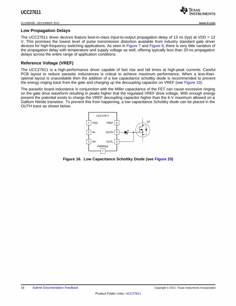
The UCC27611 is a high-performance driver capable of fast rise and fall times at high-peak currents. CarefulPCB layout to reduce parasitic inductances is critical to achieve maximum performance. When a less-than-optimal layout is unavoidable then the addition of a low capacitance schottky diode is recommended to preventthe energy ringing back from the gate and charging up the decoupling capacitor on VREF (see Figure 19).
The parasitic board inductance in conjunction with the Miller capacitance of the FET can cause excessive ringingon the gate drive waveform resulting in peaks higher that the regulated VREF drive voltage. With enough energypresent the potential exists to charge the VREF decoupling capacitor higher than the 6-V maximum allowed on aGallium Nitride transistor. To prevent this from happening, a low capacitance Schottky diode can be placed in theOUTH trace as shown below.
Figure 16. Low Capacitance Schottky Diode (see Figure 20)
16 Submit Documentation Feedback Copyright © 2012, Texas Instruments Incorporated
Product Folder Links: UCC27611
1
2
3
6
5
4
VDD
IN-
IN+
VREF
OUTH
OUTL
UCC27611
7
PWRPAD
D1
Q1
1
2
3
6
5
4
VDD
IN-
IN+
VREF
OUTH
OUTL
UCC27611
7
PWRPAD
D2
Q2
VIN
1
2
3
6
5
4
VDD
IN-
IN+
VREF
OUTH
OUTL
UCC27611
7
PWRPAD
Q1
R1
C1 R2
UCC27611
www.ti.com SLUSBA5B –DECEMBER 2012
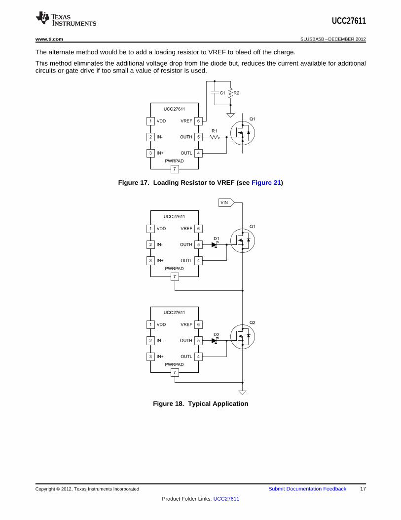
The alternate method would be to add a loading resistor to VREF to bleed off the charge.
This method eliminates the additional voltage drop from the diode but, reduces the current available for additionalcircuits or gate drive if too small a value of resistor is used.
Figure 17. Loading Resistor to VREF (see Figure 21)
Figure 18. Typical Application
Copyright © 2012, Texas Instruments Incorporated Submit Documentation Feedback 17
Product Folder Links: UCC27611
0
2
4
6
8
10
12
15 25 35 45 55 65VIN (V)
VR
EF
Loa
d (m
A)
G001
4.8
4.9
5
5.1
5.2
5.3
5.4
5.5
5 10 15 20 25 30 35VIN (V)
VR
EF
(V
)
G001
4.8
4.9
5
5 15 25 35 45 55 65VIN (V)
VR
EF
(V
)
G001
UCC27611
SLUSBA5B –DECEMBER 2012 www.ti.com
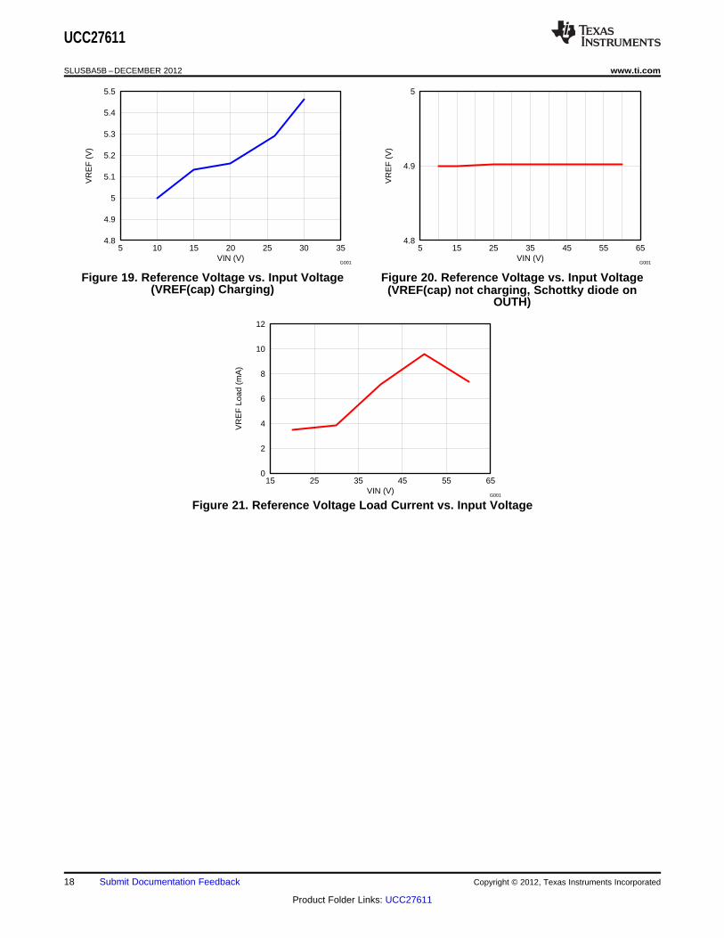
Figure 19. Reference Voltage vs. Input Voltage Figure 20. Reference Voltage vs. Input Voltage(VREF(cap) Charging) (VREF(cap) not charging, Schottky diode on
OUTH)
Figure 21. Reference Voltage Load Current vs. Input Voltage
18 Submit Documentation Feedback Copyright © 2012, Texas Instruments Incorporated
Product Folder Links: UCC27611
UCC27611
www.ti.com SLUSBA5B –DECEMBER 2012
Thermal Information
The useful range of a driver is greatly affected by the drive power requirements of the load and the thermalcharacteristics of the package. In order for a gate driver to be useful over a particular temperature range thepackage must allow for the efficient removal of the heat produced while keeping the junction temperature withinrated limits. The thermal metrics for the driver package is summarized in the Thermal Information section of thedatasheet. For detailed information regarding the thermal information table, please refer to the Application Notefrom Texas Instruments entitled IC Package Thermal Metrics (Texas Instruments Literature Number SPRA953A).
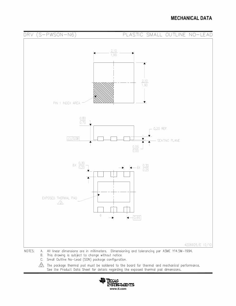
UCC27611 Offered in WSON, 7-Pin Package (DRV)
6-pin package with exposed thermal pad. The thermal information table summarizes the thermal performancemetrics related to the two packages. θJA metric should be used for comparison of power dissipation betweendifferent packages. Under identical power dissipation conditions, the DRS package will maintain a lower dietemperature than the DBV. The ψJT and ψJB metrics should be used when estimating the die temperature duringactual application measurements.
The DRV is a better thermal package overall because it has the exposed thermal pad and is able to sink heat tothe PCB. The thermal pad in DRV package provides designers with an ability to create an excellent heat removalsub-system from the vicinity of the device, thus helping to maintain a lower junction temperature. This pad shouldbe soldered to the copper on the printed circuit board directly underneath the device package. Then a printedcircuit board designed with thermal lands and thermal vias completes a very efficient heat removal subsystem. Insuch a design, the heat is extracted from the semiconductor junction through the thermal pad, which is thenefficiently conducted away from the location of the device on the PCB through the thermal network. This helps tomaintain a lower board temperature near the vicinity of the device leading to an overall lower device junctiontemperature.
NOTEThe exposed pad in DRV package is directly connected to the GND of the internalcircuitry. It is electrically and thermally connected to the device which is the ground of thedevice. It is required to externally connect the exposed pad to GND in PCB layout.
Copyright © 2012, Texas Instruments Incorporated Submit Documentation Feedback 19
Product Folder Links: UCC27611
UCC27611
SLUSBA5B –DECEMBER 2012 www.ti.com
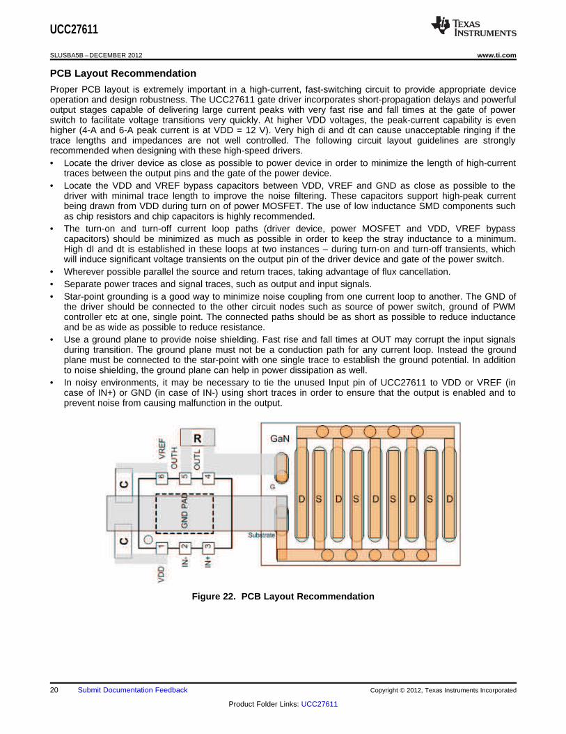
PCB Layout Recommendation
Proper PCB layout is extremely important in a high-current, fast-switching circuit to provide appropriate deviceoperation and design robustness. The UCC27611 gate driver incorporates short-propagation delays and powerfuloutput stages capable of delivering large current peaks with very fast rise and fall times at the gate of powerswitch to facilitate voltage transitions very quickly. At higher VDD voltages, the peak-current capability is evenhigher (4-A and 6-A peak current is at VDD = 12 V). Very high di and dt can cause unacceptable ringing if thetrace lengths and impedances are not well controlled. The following circuit layout guidelines are stronglyrecommended when designing with these high-speed drivers.• Locate the driver device as close as possible to power device in order to minimize the length of high-current
traces between the output pins and the gate of the power device.• Locate the VDD and VREF bypass capacitors between VDD, VREF and GND as close as possible to the
driver with minimal trace length to improve the noise filtering. These capacitors support high-peak currentbeing drawn from VDD during turn on of power MOSFET. The use of low inductance SMD components suchas chip resistors and chip capacitors is highly recommended.
• The turn-on and turn-off current loop paths (driver device, power MOSFET and VDD, VREF bypasscapacitors) should be minimized as much as possible in order to keep the stray inductance to a minimum.High dI and dt is established in these loops at two instances – during turn-on and turn-off transients, whichwill induce significant voltage transients on the output pin of the driver device and gate of the power switch.
• Wherever possible parallel the source and return traces, taking advantage of flux cancellation.• Separate power traces and signal traces, such as output and input signals.• Star-point grounding is a good way to minimize noise coupling from one current loop to another. The GND of
the driver should be connected to the other circuit nodes such as source of power switch, ground of PWMcontroller etc at one, single point. The connected paths should be as short as possible to reduce inductanceand be as wide as possible to reduce resistance.
• Use a ground plane to provide noise shielding. Fast rise and fall times at OUT may corrupt the input signalsduring transition. The ground plane must not be a conduction path for any current loop. Instead the groundplane must be connected to the star-point with one single trace to establish the ground potential. In additionto noise shielding, the ground plane can help in power dissipation as well.
• In noisy environments, it may be necessary to tie the unused Input pin of UCC27611 to VDD or VREF (incase of IN+) or GND (in case of IN-) using short traces in order to ensure that the output is enabled and toprevent noise from causing malfunction in the output.
Figure 22. PCB Layout Recommendation
20 Submit Documentation Feedback Copyright © 2012, Texas Instruments Incorporated
Product Folder Links: UCC27611
UCC27611
www.ti.com SLUSBA5B –DECEMBER 2012
REVISION HISTORY
Changes from Original (December 2012) to Revision A Page
• Changed marketing status from Product Preview to Production Data. ................................................................................ 1
Changes from Revision A (December, 2012) to Revision B Page
• Added ELECTRICAL CHARACTERISTICS Inputs (IN+, IN-) section values. ..................................................................... 4
Copyright © 2012, Texas Instruments Incorporated Submit Documentation Feedback 21
Product Folder Links: UCC27611
PACKAGE OPTION ADDENDUM
www.ti.com 17-May-2013
Addendum-Page 1
PACKAGING INFORMATION
Orderable Device Status(1)
Package Type PackageDrawing
Pins PackageQty
Eco Plan(2)
Lead/Ball Finish MSL Peak Temp(3)
Op Temp (°C) Device Marking(4/5)
Samples
UCC27611DRVR ACTIVE SON DRV 6 3000 Green (RoHS& no Sb/Br)
CU NIPDAU Level-2-260C-1 YEAR -40 to 140 7611
UCC27611DRVT ACTIVE SON DRV 6 250 Green (RoHS& no Sb/Br)
CU NIPDAU Level-2-260C-1 YEAR -40 to 140 7611
(1) The marketing status values are defined as follows:ACTIVE: Product device recommended for new designs.LIFEBUY: TI has announced that the device will be discontinued, and a lifetime-buy period is in effect.NRND: Not recommended for new designs. Device is in production to support existing customers, but TI does not recommend using this part in a new design.PREVIEW: Device has been announced but is not in production. Samples may or may not be available.OBSOLETE: TI has discontinued the production of the device.
(2) Eco Plan - The planned eco-friendly classification: Pb-Free (RoHS), Pb-Free (RoHS Exempt), or Green (RoHS & no Sb/Br) - please check http://www.ti.com/productcontent for the latest availabilityinformation and additional product content details.TBD: The Pb-Free/Green conversion plan has not been defined.Pb-Free (RoHS): TI's terms "Lead-Free" or "Pb-Free" mean semiconductor products that are compatible with the current RoHS requirements for all 6 substances, including the requirement thatlead not exceed 0.1% by weight in homogeneous materials. Where designed to be soldered at high temperatures, TI Pb-Free products are suitable for use in specified lead-free processes.Pb-Free (RoHS Exempt): This component has a RoHS exemption for either 1) lead-based flip-chip solder bumps used between the die and package, or 2) lead-based die adhesive used betweenthe die and leadframe. The component is otherwise considered Pb-Free (RoHS compatible) as defined above.Green (RoHS & no Sb/Br): TI defines "Green" to mean Pb-Free (RoHS compatible), and free of Bromine (Br) and Antimony (Sb) based flame retardants (Br or Sb do not exceed 0.1% by weightin homogeneous material)
(3) MSL, Peak Temp. -- The Moisture Sensitivity Level rating according to the JEDEC industry standard classifications, and peak solder temperature.
(4) There may be additional marking, which relates to the logo, the lot trace code information, or the environmental category on the device.
(5) Multiple Device Markings will be inside parentheses. Only one Device Marking contained in parentheses and separated by a "~" will appear on a device. If a line is indented then it is a continuationof the previous line and the two combined represent the entire Device Marking for that device.
Important Information and Disclaimer:The information provided on this page represents TI's knowledge and belief as of the date that it is provided. TI bases its knowledge and belief on informationprovided by third parties, and makes no representation or warranty as to the accuracy of such information. Efforts are underway to better integrate information from third parties. TI has taken andcontinues to take reasonable steps to provide representative and accurate information but may not have conducted destructive testing or chemical analysis on incoming materials and chemicals.TI and TI suppliers consider certain information to be proprietary, and thus CAS numbers and other limited information may not be available for release.
In no event shall TI's liability arising out of such information exceed the total purchase price of the TI part(s) at issue in this document sold by TI to Customer on an annual basis.
TAPE AND REEL INFORMATION
*All dimensions are nominal
Device PackageType
PackageDrawing
Pins SPQ ReelDiameter
(mm)
ReelWidth
W1 (mm)
A0(mm)
B0(mm)
K0(mm)
P1(mm)
W(mm)
Pin1Quadrant
UCC27611DRVR SON DRV 6 3000 180.0 8.4 2.3 2.3 1.15 4.0 8.0 Q2
UCC27611DRVT SON DRV 6 250 180.0 8.4 2.3 2.3 1.15 4.0 8.0 Q2
PACKAGE MATERIALS INFORMATION
www.ti.com 7-Sep-2013
Pack Materials-Page 1
*All dimensions are nominal
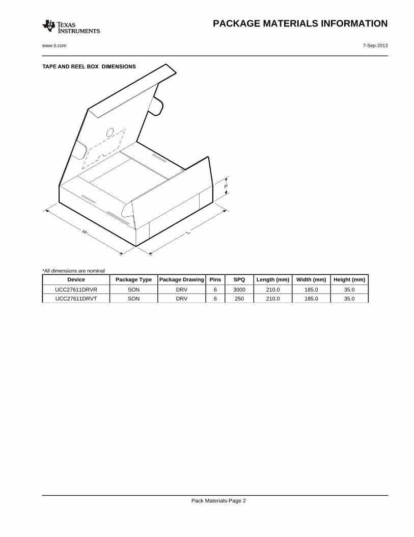
Device Package Type Package Drawing Pins SPQ Length (mm) Width (mm) Height (mm)
UCC27611DRVR SON DRV 6 3000 210.0 185.0 35.0
UCC27611DRVT SON DRV 6 250 210.0 185.0 35.0
PACKAGE MATERIALS INFORMATION
www.ti.com 7-Sep-2013
Pack Materials-Page 2

IMPORTANT NOTICE
Texas Instruments Incorporated and its subsidiaries (TI) reserve the right to make corrections, enhancements, improvements and otherchanges to its semiconductor products and services per JESD46, latest issue, and to discontinue any product or service per JESD48, latestissue. Buyers should obtain the latest relevant information before placing orders and should verify that such information is current andcomplete. All semiconductor products (also referred to herein as “components”) are sold subject to TI’s terms and conditions of salesupplied at the time of order acknowledgment.
TI warrants performance of its components to the specifications applicable at the time of sale, in accordance with the warranty in TI’s termsand conditions of sale of semiconductor products. Testing and other quality control techniques are used to the extent TI deems necessaryto support this warranty. Except where mandated by applicable law, testing of all parameters of each component is not necessarilyperformed.
TI assumes no liability for applications assistance or the design of Buyers’ products. Buyers are responsible for their products andapplications using TI components. To minimize the risks associated with Buyers’ products and applications, Buyers should provideadequate design and operating safeguards.
TI does not warrant or represent that any license, either express or implied, is granted under any patent right, copyright, mask work right, orother intellectual property right relating to any combination, machine, or process in which TI components or services are used. Informationpublished by TI regarding third-party products or services does not constitute a license to use such products or services or a warranty orendorsement thereof. Use of such information may require a license from a third party under the patents or other intellectual property of thethird party, or a license from TI under the patents or other intellectual property of TI.
Reproduction of significant portions of TI information in TI data books or data sheets is permissible only if reproduction is without alterationand is accompanied by all associated warranties, conditions, limitations, and notices. TI is not responsible or liable for such altereddocumentation. Information of third parties may be subject to additional restrictions.
Resale of TI components or services with statements different from or beyond the parameters stated by TI for that component or servicevoids all express and any implied warranties for the associated TI component or service and is an unfair and deceptive business practice.TI is not responsible or liable for any such statements.
Buyer acknowledges and agrees that it is solely responsible for compliance with all legal, regulatory and safety-related requirementsconcerning its products, and any use of TI components in its applications, notwithstanding any applications-related information or supportthat may be provided by TI. Buyer represents and agrees that it has all the necessary expertise to create and implement safeguards whichanticipate dangerous consequences of failures, monitor failures and their consequences, lessen the likelihood of failures that might causeharm and take appropriate remedial actions. Buyer will fully indemnify TI and its representatives against any damages arising out of the useof any TI components in safety-critical applications.
In some cases, TI components may be promoted specifically to facilitate safety-related applications. With such components, TI’s goal is tohelp enable customers to design and create their own end-product solutions that meet applicable functional safety standards andrequirements. Nonetheless, such components are subject to these terms.
No TI components are authorized for use in FDA Class III (or similar life-critical medical equipment) unless authorized officers of the partieshave executed a special agreement specifically governing such use.
Only those TI components which TI has specifically designated as military grade or “enhanced plastic” are designed and intended for use inmilitary/aerospace applications or environments. Buyer acknowledges and agrees that any military or aerospace use of TI componentswhich have not been so designated is solely at the Buyer's risk, and that Buyer is solely responsible for compliance with all legal andregulatory requirements in connection with such use.
TI has specifically designated certain components as meeting ISO/TS16949 requirements, mainly for automotive use. In any case of use ofnon-designated products, TI will not be responsible for any failure to meet ISO/TS16949.
Products Applications
Audio www.ti.com/audio Automotive and Transportation www.ti.com/automotive
Amplifiers amplifier.ti.com Communications and Telecom www.ti.com/communications
Data Converters dataconverter.ti.com Computers and Peripherals www.ti.com/computers
DLP® Products www.dlp.com Consumer Electronics www.ti.com/consumer-apps
DSP dsp.ti.com Energy and Lighting www.ti.com/energy
Clocks and Timers www.ti.com/clocks Industrial www.ti.com/industrial
Interface interface.ti.com Medical www.ti.com/medical
Logic logic.ti.com Security www.ti.com/security
Power Mgmt power.ti.com Space, Avionics and Defense www.ti.com/space-avionics-defense
Microcontrollers microcontroller.ti.com Video and Imaging www.ti.com/video
RFID www.ti-rfid.com
OMAP Applications Processors www.ti.com/omap TI E2E Community e2e.ti.com
Wireless Connectivity www.ti.com/wirelessconnectivity
Mailing Address: Texas Instruments, Post Office Box 655303, Dallas, Texas 75265Copyright © 2013, Texas Instruments Incorporated