Embed Size (px)
Citation preview
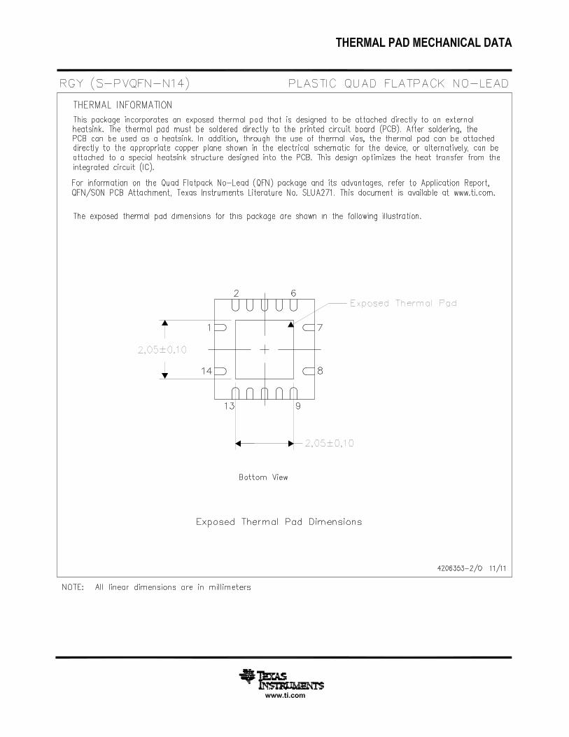
14
13
12
11
10
9
8
1
2
3
4
5
6
7 OE
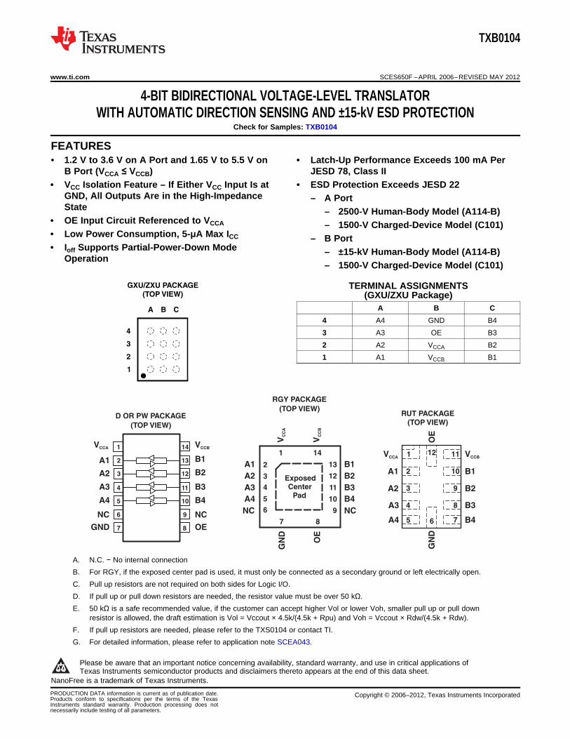
D OR PW PACKAGE
(TOP VIEW)
GND
NC
A4
A3
A2
VCCA
NC
B4
B3
B2
B1
VCCB
A1
RGY PACKAGE
ExposedCenter
Pad
(TOP VIEW)
1 14
7 8
2
3
4
5
6
13
12
11
10
9
B1
B2
B3
B4
NC
A1
A2
A3
A4
NC
OE
VC
CB
GN
DV
CC
A
VCCB
B1
B2
B3
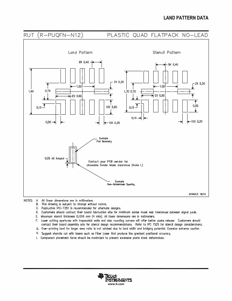
RUT PACKAGE
(TOP VIEW)
3
2
6
10
1
4 8
9
1112
A2
A3
VCCA
A1
OE
GN
D
B45 7A4
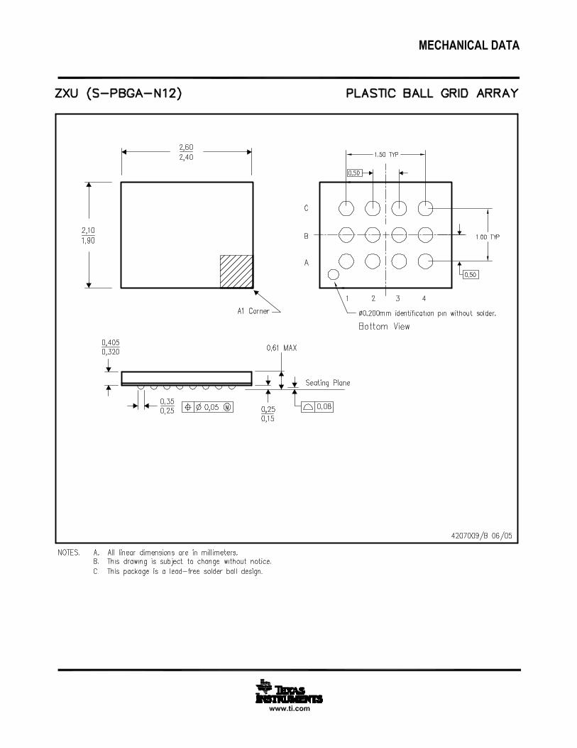
GXU/ZXU PACKAGE
(TOP VIEW)
4
3
2
1
A B C
TXB0104
www.ti.com SCES650F –APRIL 2006–REVISED MAY 2012
4-BIT BIDIRECTIONAL VOLTAGE-LEVEL TRANSLATORWITH AUTOMATIC DIRECTION SENSING AND ±15-kV ESD PROTECTION
Check for Samples: TXB0104
1FEATURES2• 1.2 V to 3.6 V on A Port and 1.65 V to 5.5 V on • Latch-Up Performance Exceeds 100 mA Per
B Port (VCCA ≤ VCCB) JESD 78, Class II• VCC Isolation Feature – If Either VCC Input Is at • ESD Protection Exceeds JESD 22
GND, All Outputs Are in the High-Impedance – A PortState – 2500-V Human-Body Model (A114-B)
• OE Input Circuit Referenced to VCCA – 1500-V Charged-Device Model (C101)• Low Power Consumption, 5-μA Max ICC – B Port• Ioff Supports Partial-Power-Down Mode – ±15-kV Human-Body Model (A114-B)
Operation– 1500-V Charged-Device Model (C101)
TERMINAL ASSIGNMENTS(GXU/ZXU Package)
A B C
4 A4 GND B4
3 A3 OE B3
2 A2 VCCA B2
1 A1 VCCB B1
A. N.C. − No internal connection
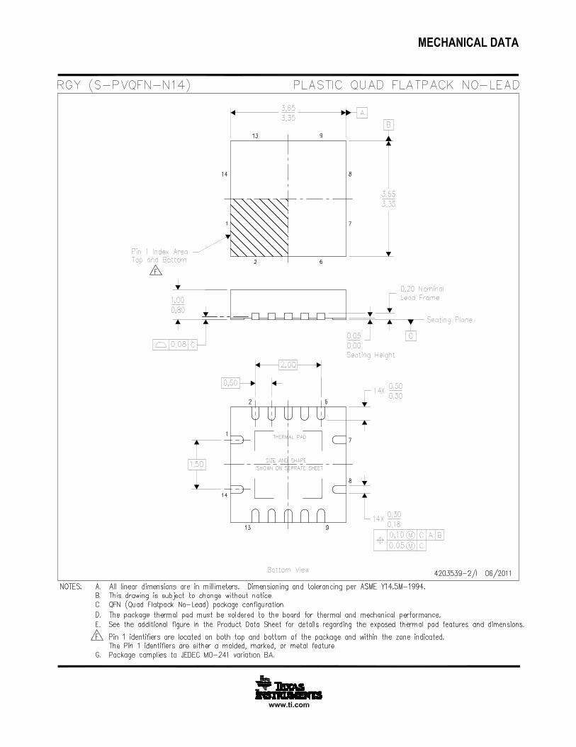
B. For RGY, if the exposed center pad is used, it must only be connected as a secondary ground or left electrically open.
C. Pull up resistors are not required on both sides for Logic I/O.
D. If pull up or pull down resistors are needed, the resistor value must be over 50 kΩ.
E. 50 kΩ is a safe recommended value, if the customer can accept higher Vol or lower Voh, smaller pull up or pull downresistor is allowed, the draft estimation is Vol = Vccout × 4.5k/(4.5k + Rpu) and Voh = Vccout × Rdw/(4.5k + Rdw).
F. If pull up resistors are needed, please refer to the TXS0104 or contact TI.
G. For detailed information, please refer to application note SCEA043.
1
Please be aware that an important notice concerning availability, standard warranty, and use in critical applications ofTexas Instruments semiconductor products and disclaimers thereto appears at the end of this data sheet.
2NanoFree is a trademark of Texas Instruments.
PRODUCTION DATA information is current as of publication date. Copyright © 2006–2012, Texas Instruments IncorporatedProducts conform to specifications per the terms of the TexasInstruments standard warranty. Production processing does notnecessarily include testing of all parameters.

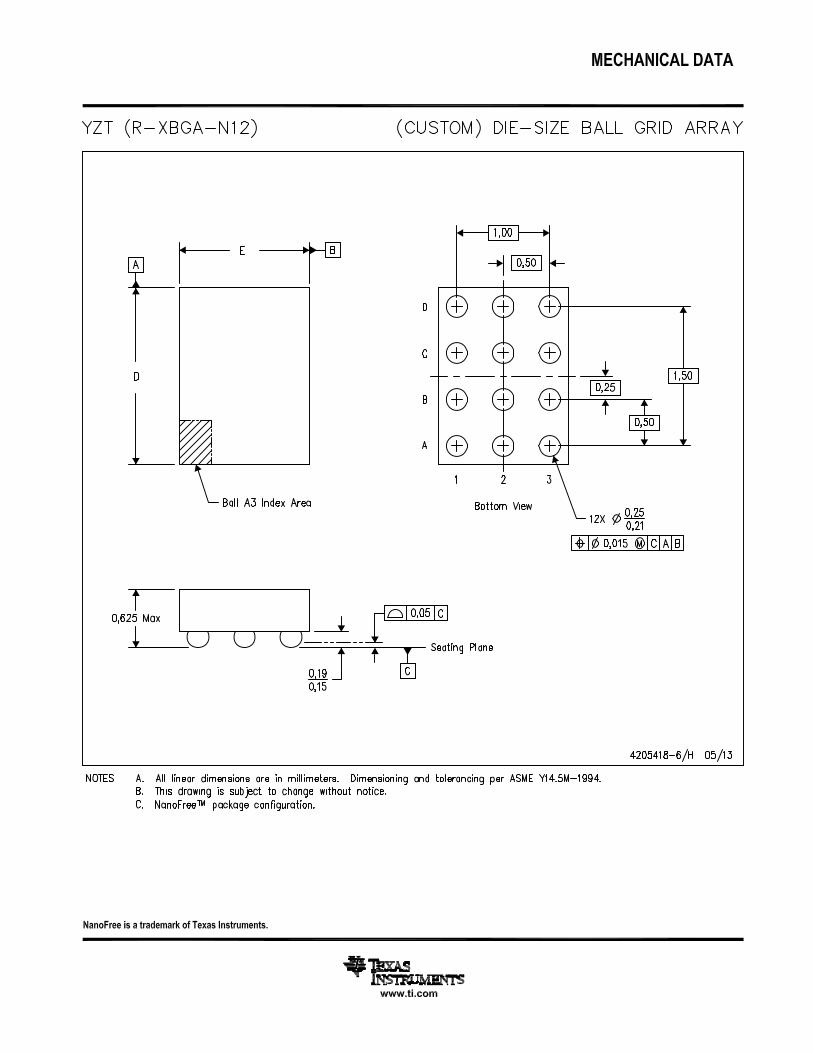
YZT PACKAGE
(TOP VIEW)
D
C
B
A
3 2 1
TXB0104
SCES650F –APRIL 2006–REVISED MAY 2012 www.ti.com
These devices have limited built-in ESD protection. The leads should be shorted together or the device placed in conductive foamduring storage or handling to prevent electrostatic damage to the MOS gates.
TERMINAL ASSIGNMENTS(YZT Package)3 2 1
D A4 GND B4
C A3 OE B3
B A2 VCCA B2
A A1 VCCB B1
DESCRIPTION/ORDERING INFORMATIONThis 4-bit noninverting translator uses two separate configurable power-supply rails. The A port is designed totrack VCCA. VCCA accepts any supply voltage from 1.2 V to 3.6 V. The B port is designed to track VCCB. VCCBaccepts any supply voltage from 1.65 V to 5.5 V. This allows for universal low-voltage bidirectional translationbetween any of the 1.2-V, 1.5-V, 1.8-V, 2.5-V, 3.3-V, and 5-V voltage nodes. VCCA should not exceed VCCB.
When the output-enable (OE) input is low, all outputs are placed in the high-impedance state. To ensure thehigh-impedance state during power up or power down, OE should be tied to GND through a pulldown resistor;the minimum value of the resistor is determined by the current-sourcing capability of the driver.
The TXB0104 is designed so that the OE input circuit is supplied by VCCA.
This device is fully specified for partial-power-down applications using Ioff. The Ioff circuitry disables the outputs,preventing damaging current backflow through the device when it is powered down.
ORDERING INFORMATION (1)
TA PACKAGE (2) ORDERABLE PART NUMBER TOP-SIDE MARKING (3)
NanoFree™ — WCSP (DSBGA)0.23-mm Large Bump – YZT Reel of 3000 TXB0104YZTR _ _ _ 2 K _(Pb-free) 0.625-mm max height
UFBGA – GXU Reel of 2500 TXB0104GXUR YE04
UFBGA – ZXU (Pb-Free) Reel of 2500 TXB0104ZXUR YE04
TXB0104RGYRQFN – RGY Reel of 1000 YE04
TXB0104RGYRG4–40°C to 85°C uQFN – RUT Reel of 3000 TXB0104RUTR 2KR
TXB0104DTube of 50
TXB0104DG4SOIC – D TXB0104
TXB0104DRReel of 2500
TXB0104DRG4
TXB0104PWRTSSOP – PW Reel of 2000 YE04
TXB0104PWRG4
(1) For the most current package and ordering information, see the Package Option Addendum at the end of this document, or see the TIweb site at www.ti.com.
(2) Package drawings, thermal data, and symbolization are available at www.ti.com/packaging.(3) YZT: The actual top-side marking has three preceding characters to denote year, month, and sequence code, and one following
character to designate the wafer fab/assembly site. Pin 1 identifier indicates solder-bump composition (1 = SnPb, • = Pb-free).
2 Submit Documentation Feedback Copyright © 2006–2012, Texas Instruments Incorporated
Product Folder Links: TXB0104

TXB0104
www.ti.com SCES650F –APRIL 2006–REVISED MAY 2012
PIN DESCRIPTIONPIN NO. BALL NO.
NAME FUNCTIOND, PW, GXU/RUT YZTOR RGY ZXU
1 1 B2 B2 VCCA A-port supply voltage 1.2 V ≤ VCCA ≤ 3.6 V and VCCA ≤ VCCB.
2 2 A1 A3 A1 Input/output 1. Referenced to VCCA.
3 3 A2 B3 A2 Input/output 2. Referenced to VCCA.
4 4 A3 C3 A3 Input/output 3. Referenced to VCCA.
5 5 A4 D3 A4 Input/output 4. Referenced to VCCA.
6 – – – NC No connection. Not internally connected.
7 6 B4 D2 GND Ground
3-state output-mode enable. Pull OE low to place all outputs in 3-state mode.8 12 B3 C2 OE Referenced to VCCA.
9 – – – NC No connection. Not internally connected.
10 7 C4 D1 B4 Input/output 4. Referenced to VCCB.
11 8 C3 C1 B3 Input/output 3. Referenced to VCCB.
12 9 C2 B1 B2 Input/output 2. Referenced to VCCB.
13 10 C1 A1 B1 Input/output 1. Referenced to VCCB.
14 11 B1 A2 VCCB B-port supply voltage 1.65 V ≤ VCCB ≤ 5.5 V.
ABSOLUTE MAXIMUM RATINGS (1)
over operating free-air temperature range (unless otherwise noted)
MIN MAX UNIT
VCCA –0.5 4.6Supply voltage range V
VCCB –0.5 6.5
A port –0.5 4.6VI Input voltage range V
B port –0.5 6.5
A port –0.5 4.6Voltage range applied to any output in the high-impedance orVO Vpower-off state B port -0.5 6.5
A port –0.5 VCCA + 0.5VO Voltage range applied to any output in the high or low state (2) V
B port –0.5 VCCB + 0.5
IIK Input clamp current VI < 0 –50 mA
IOK Output clamp current VO < 0 –50 mA
IO Continuous output current ±50 mA
Continuous current through VCCA, VCCB, or GND ±100 mA
Tstg Storage temperature range –65 150 °C
(1) Stresses beyond those listed under "absolute maximum ratings" may cause permanent damage to the device. These are stress ratingsonly, and functional operation of the device at these or any other conditions beyond those indicated under "recommended operatingconditions" is not implied. Exposure to absolute-maximum-rated conditions for extended periods may affect device reliability.
(2) The value of VCCA and VCCB are provided in the recommended operating conditions table.
Copyright © 2006–2012, Texas Instruments Incorporated Submit Documentation Feedback 3
Product Folder Links: TXB0104
TXB0104
SCES650F –APRIL 2006–REVISED MAY 2012 www.ti.com
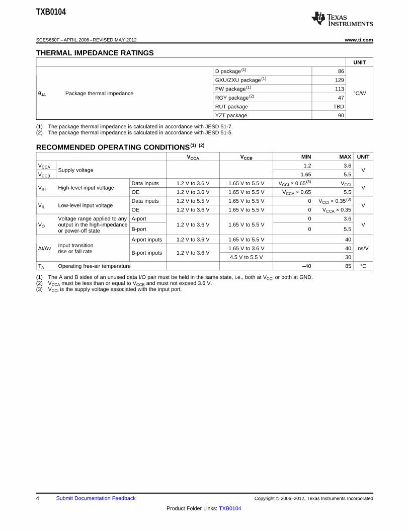
THERMAL IMPEDANCE RATINGSUNIT
D package (1) 86
GXU/ZXU package (1) 129
PW package (1) 113θJA Package thermal impedance °C/W
RGY package (2) 47
RUT package TBD
YZT package 90
(1) The package thermal impedance is calculated in accordance with JESD 51-7.(2) The package thermal impedance is calculated in accordance with JESD 51-5.
RECOMMENDED OPERATING CONDITIONS (1) (2)
VCCA VCCB MIN MAX UNIT
VCCA 1.2 3.6Supply voltage V
VCCB 1.65 5.5
Data inputs 1.2 V to 3.6 V 1.65 V to 5.5 V VCCI × 0.65 (3) VCCIVIH High-level input voltage V
OE 1.2 V to 3.6 V 1.65 V to 5.5 V VCCA × 0.65 5.5
Data inputs 1.2 V to 5.5 V 1.65 V to 5.5 V 0 VCCI × 0.35 (3)
VIL Low-level input voltage VOE 1.2 V to 3.6 V 1.65 V to 5.5 V 0 VCCA × 0.35
Voltage range applied to any A-port 0 3.6VO output in the high-impedance 1.2 V to 3.6 V 1.65 V to 5.5 V V
B-port 0 5.5or power-off state
A-port inputs 1.2 V to 3.6 V 1.65 V to 5.5 V 40Input transitionΔt/Δv 1.65 V to 3.6 V 40 ns/Vrise or fall rate B-port inputs 1.2 V to 3.6 V
4.5 V to 5.5 V 30
TA Operating free-air temperature –40 85 °C
(1) The A and B sides of an unused data I/O pair must be held in the same state, i.e., both at VCCI or both at GND.(2) VCCA must be less than or equal to VCCB and must not exceed 3.6 V.(3) VCCI is the supply voltage associated with the input port.
4 Submit Documentation Feedback Copyright © 2006–2012, Texas Instruments Incorporated
Product Folder Links: TXB0104
TXB0104
www.ti.com SCES650F –APRIL 2006–REVISED MAY 2012
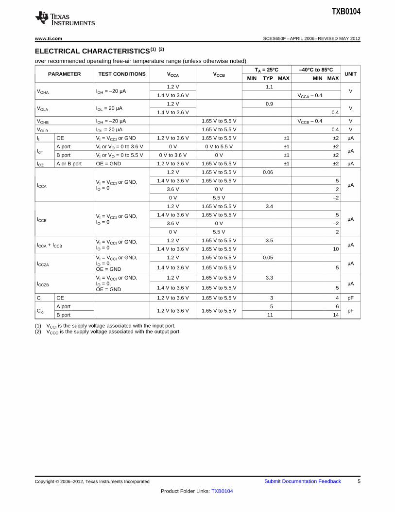
ELECTRICAL CHARACTERISTICS (1) (2)
over recommended operating free-air temperature range (unless otherwise noted)
TA = 25°C –40°C to 85°CPARAMETER TEST CONDITIONS VCCA VCCB UNIT
MIN TYP MAX MIN MAX
1.2 V 1.1VOHA IOH = –20 μA V
1.4 V to 3.6 V VCCA – 0.4
1.2 V 0.9VOLA IOL = 20 μA V
1.4 V to 3.6 V 0.4
VOHB IOH = –20 μA 1.65 V to 5.5 V VCCB – 0.4 V
VOLB IOL = 20 μA 1.65 V to 5.5 V 0.4 V
II OE VI = VCCI or GND 1.2 V to 3.6 V 1.65 V to 5.5 V ±1 ±2 μA
A port VI or VO = 0 to 3.6 V 0 V 0 V to 5.5 V ±1 ±2Ioff μA
B port VI or VO = 0 to 5.5 V 0 V to 3.6 V 0 V ±1 ±2
IOZ A or B port OE = GND 1.2 V to 3.6 V 1.65 V to 5.5 V ±1 ±2 μA
1.2 V 1.65 V to 5.5 V 0.06
1.4 V to 3.6 V 1.65 V to 5.5 V 5VI = VCCI or GND,ICCA μAIO = 0 3.6 V 0 V 2
0 V 5.5 V –2
1.2 V 1.65 V to 5.5 V 3.4
1.4 V to 3.6 V 1.65 V to 5.5 V 5VI = VCCI or GND,ICCB μAIO = 0 3.6 V 0 V –2
0 V 5.5 V 2
1.2 V 1.65 V to 5.5 V 3.5VI = VCCI or GND,ICCA + ICCB μAIO = 0 1.4 V to 3.6 V 1.65 V to 5.5 V 10
VI = VCCI or GND, 1.2 V 1.65 V to 5.5 V 0.05ICCZA IO = 0, μA
1.4 V to 3.6 V 1.65 V to 5.5 V 5OE = GND
VI = VCCI or GND, 1.2 V 1.65 V to 5.5 V 3.3ICCZB IO = 0, μA
1.4 V to 3.6 V 1.65 V to 5.5 V 5OE = GND
Ci OE 1.2 V to 3.6 V 1.65 V to 5.5 V 3 4 pF
A port 5 6Cio 1.2 V to 3.6 V 1.65 V to 5.5 V pF
B port 11 14
(1) VCCI is the supply voltage associated with the input port.(2) VCCO is the supply voltage associated with the output port.
Copyright © 2006–2012, Texas Instruments Incorporated Submit Documentation Feedback 5
Product Folder Links: TXB0104
TXB0104
SCES650F –APRIL 2006–REVISED MAY 2012 www.ti.com
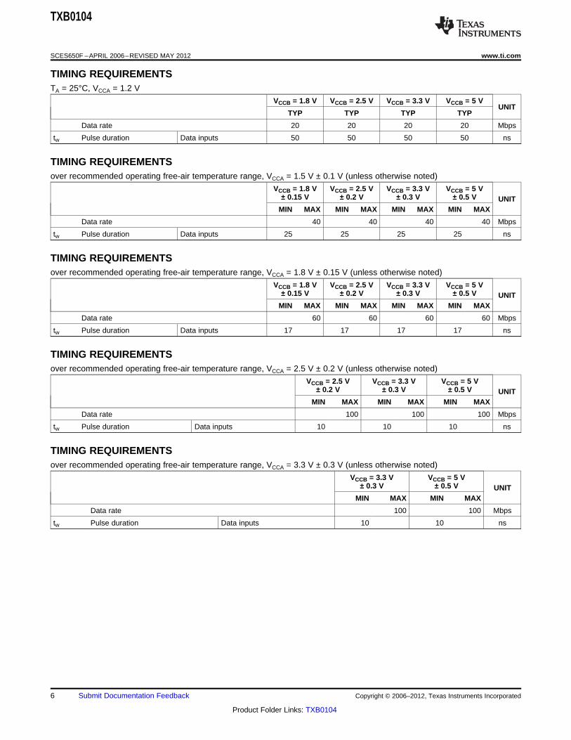
TIMING REQUIREMENTSTA = 25°C, VCCA = 1.2 V
VCCB = 1.8 V VCCB = 2.5 V VCCB = 3.3 V VCCB = 5 VUNIT
TYP TYP TYP TYP
Data rate 20 20 20 20 Mbps
tw Pulse duration Data inputs 50 50 50 50 ns
TIMING REQUIREMENTSover recommended operating free-air temperature range, VCCA = 1.5 V ± 0.1 V (unless otherwise noted)
VCCB = 1.8 V VCCB = 2.5 V VCCB = 3.3 V VCCB = 5 V± 0.15 V ± 0.2 V ± 0.3 V ± 0.5 V UNIT
MIN MAX MIN MAX MIN MAX MIN MAX
Data rate 40 40 40 40 Mbps
tw Pulse duration Data inputs 25 25 25 25 ns
TIMING REQUIREMENTSover recommended operating free-air temperature range, VCCA = 1.8 V ± 0.15 V (unless otherwise noted)
VCCB = 1.8 V VCCB = 2.5 V VCCB = 3.3 V VCCB = 5 V± 0.15 V ± 0.2 V ± 0.3 V ± 0.5 V UNIT
MIN MAX MIN MAX MIN MAX MIN MAX
Data rate 60 60 60 60 Mbps
tw Pulse duration Data inputs 17 17 17 17 ns
TIMING REQUIREMENTSover recommended operating free-air temperature range, VCCA = 2.5 V ± 0.2 V (unless otherwise noted)
VCCB = 2.5 V VCCB = 3.3 V VCCB = 5 V± 0.2 V ± 0.3 V ± 0.5 V UNIT
MIN MAX MIN MAX MIN MAX
Data rate 100 100 100 Mbps
tw Pulse duration Data inputs 10 10 10 ns
TIMING REQUIREMENTSover recommended operating free-air temperature range, VCCA = 3.3 V ± 0.3 V (unless otherwise noted)
VCCB = 3.3 V VCCB = 5 V± 0.3 V ± 0.5 V UNIT
MIN MAX MIN MAX
Data rate 100 100 Mbps
tw Pulse duration Data inputs 10 10 ns
6 Submit Documentation Feedback Copyright © 2006–2012, Texas Instruments Incorporated
Product Folder Links: TXB0104
TXB0104
www.ti.com SCES650F –APRIL 2006–REVISED MAY 2012
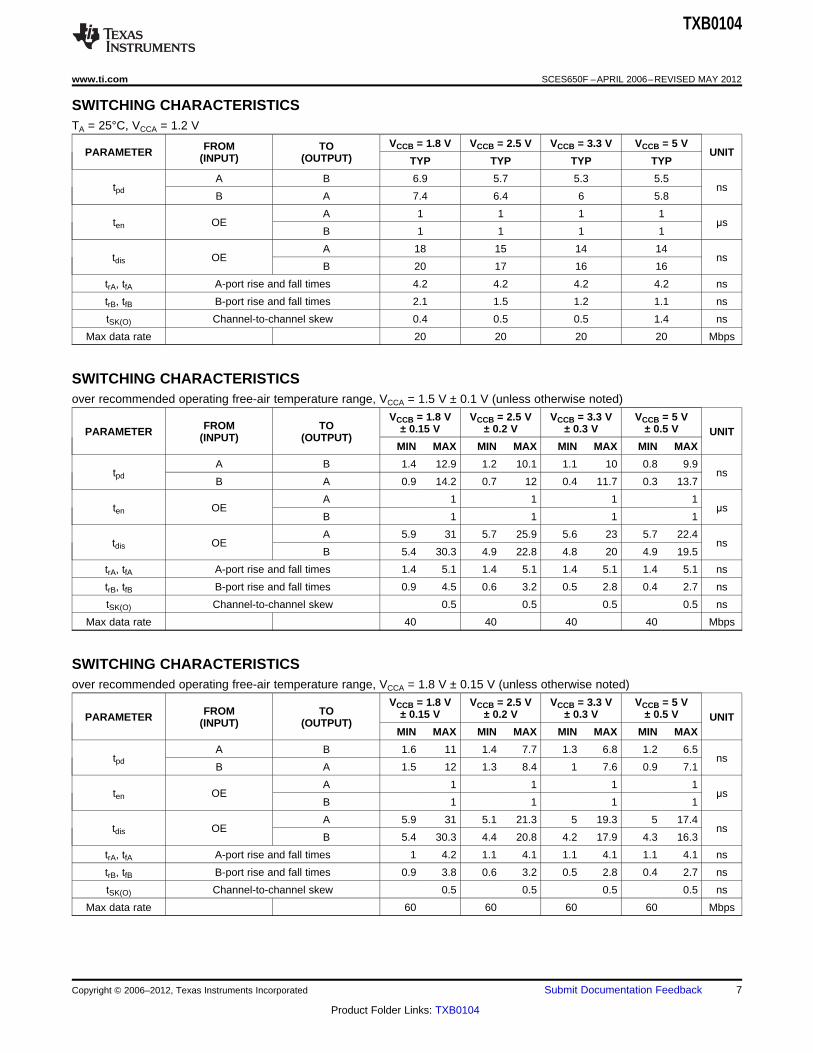
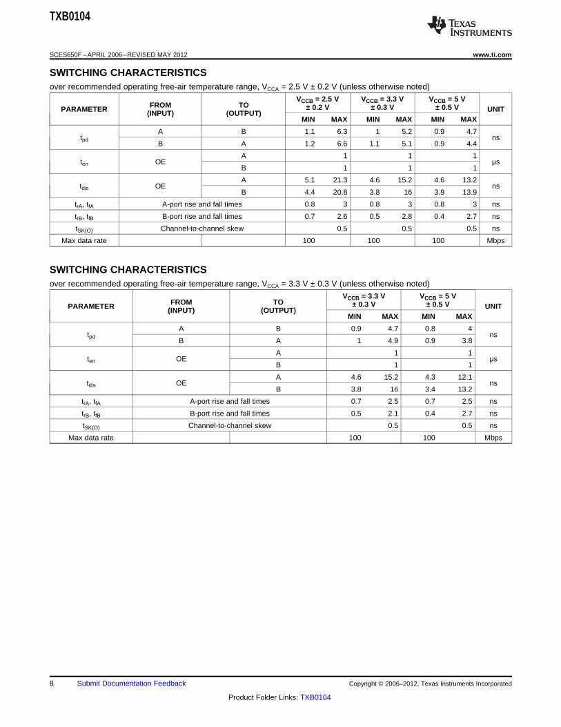
SWITCHING CHARACTERISTICSTA = 25°C, VCCA = 1.2 V
VCCB = 1.8 V VCCB = 2.5 V VCCB = 3.3 V VCCB = 5 VFROM TOPARAMETER UNIT(INPUT) (OUTPUT) TYP TYP TYP TYP
A B 6.9 5.7 5.3 5.5tpd ns
B A 7.4 6.4 6 5.8
A 1 1 1 1ten OE μs
B 1 1 1 1
A 18 15 14 14tdis OE ns
B 20 17 16 16
trA, tfA A-port rise and fall times 4.2 4.2 4.2 4.2 ns
trB, tfB B-port rise and fall times 2.1 1.5 1.2 1.1 ns
tSK(O) Channel-to-channel skew 0.4 0.5 0.5 1.4 ns
Max data rate 20 20 20 20 Mbps
SWITCHING CHARACTERISTICSover recommended operating free-air temperature range, VCCA = 1.5 V ± 0.1 V (unless otherwise noted)
VCCB = 1.8 V VCCB = 2.5 V VCCB = 3.3 V VCCB = 5 VFROM TO ± 0.15 V ± 0.2 V ± 0.3 V ± 0.5 VPARAMETER UNIT(INPUT) (OUTPUT)
MIN MAX MIN MAX MIN MAX MIN MAX
A B 1.4 12.9 1.2 10.1 1.1 10 0.8 9.9tpd ns
B A 0.9 14.2 0.7 12 0.4 11.7 0.3 13.7
A 1 1 1 1ten OE μs
B 1 1 1 1
A 5.9 31 5.7 25.9 5.6 23 5.7 22.4tdis OE ns
B 5.4 30.3 4.9 22.8 4.8 20 4.9 19.5
trA, tfA A-port rise and fall times 1.4 5.1 1.4 5.1 1.4 5.1 1.4 5.1 ns
trB, tfB B-port rise and fall times 0.9 4.5 0.6 3.2 0.5 2.8 0.4 2.7 ns
tSK(O) Channel-to-channel skew 0.5 0.5 0.5 0.5 ns
Max data rate 40 40 40 40 Mbps
SWITCHING CHARACTERISTICSover recommended operating free-air temperature range, VCCA = 1.8 V ± 0.15 V (unless otherwise noted)
VCCB = 1.8 V VCCB = 2.5 V VCCB = 3.3 V VCCB = 5 VFROM TO ± 0.15 V ± 0.2 V ± 0.3 V ± 0.5 VPARAMETER UNIT(INPUT) (OUTPUT)
MIN MAX MIN MAX MIN MAX MIN MAX
A B 1.6 11 1.4 7.7 1.3 6.8 1.2 6.5tpd ns
B A 1.5 12 1.3 8.4 1 7.6 0.9 7.1
A 1 1 1 1ten OE μs
B 1 1 1 1
A 5.9 31 5.1 21.3 5 19.3 5 17.4tdis OE ns
B 5.4 30.3 4.4 20.8 4.2 17.9 4.3 16.3
trA, tfA A-port rise and fall times 1 4.2 1.1 4.1 1.1 4.1 1.1 4.1 ns
trB, tfB B-port rise and fall times 0.9 3.8 0.6 3.2 0.5 2.8 0.4 2.7 ns
tSK(O) Channel-to-channel skew 0.5 0.5 0.5 0.5 ns
Max data rate 60 60 60 60 Mbps
Copyright © 2006–2012, Texas Instruments Incorporated Submit Documentation Feedback 7
Product Folder Links: TXB0104
TXB0104
SCES650F –APRIL 2006–REVISED MAY 2012 www.ti.com
SWITCHING CHARACTERISTICSover recommended operating free-air temperature range, VCCA = 2.5 V ± 0.2 V (unless otherwise noted)
VCCB = 2.5 V VCCB = 3.3 V VCCB = 5 VFROM TO ± 0.2 V ± 0.3 V ± 0.5 VPARAMETER UNIT(INPUT) (OUTPUT)
MIN MAX MIN MAX MIN MAX
A B 1.1 6.3 1 5.2 0.9 4.7tpd ns
B A 1.2 6.6 1.1 5.1 0.9 4.4
A 1 1 1ten OE μs
B 1 1 1
A 5.1 21.3 4.6 15.2 4.6 13.2tdis OE ns
B 4.4 20.8 3.8 16 3.9 13.9
trA, tfA A-port rise and fall times 0.8 3 0.8 3 0.8 3 ns
trB, tfB B-port rise and fall times 0.7 2.6 0.5 2.8 0.4 2.7 ns
tSK(O) Channel-to-channel skew 0.5 0.5 0.5 ns
Max data rate 100 100 100 Mbps
SWITCHING CHARACTERISTICSover recommended operating free-air temperature range, VCCA = 3.3 V ± 0.3 V (unless otherwise noted)
VCCB = 3.3 V VCCB = 5 VFROM TO ± 0.3 V ± 0.5 VPARAMETER UNIT(INPUT) (OUTPUT)
MIN MAX MIN MAX
A B 0.9 4.7 0.8 4tpd ns
B A 1 4.9 0.9 3.8
A 1 1ten OE μs
B 1 1
A 4.6 15.2 4.3 12.1tdis OE ns
B 3.8 16 3.4 13.2
trA, tfA A-port rise and fall times 0.7 2.5 0.7 2.5 ns
trB, tfB B-port rise and fall times 0.5 2.1 0.4 2.7 ns
tSK(O) Channel-to-channel skew 0.5 0.5 ns
Max data rate 100 100 Mbps
8 Submit Documentation Feedback Copyright © 2006–2012, Texas Instruments Incorporated
Product Folder Links: TXB0104
TXB0104
www.ti.com SCES650F –APRIL 2006–REVISED MAY 2012
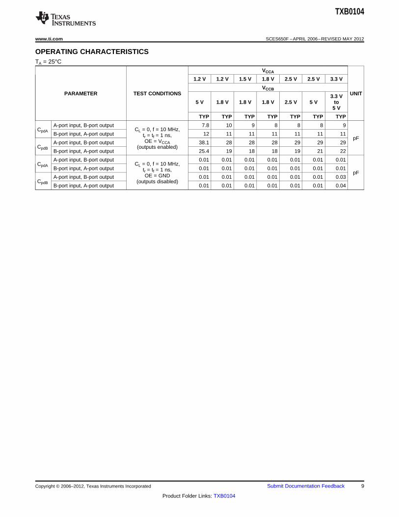
OPERATING CHARACTERISTICSTA = 25°C
VCCA
1.2 V 1.2 V 1.5 V 1.8 V 2.5 V 2.5 V 3.3 V
VCCBPARAMETER TEST CONDITIONS UNIT3.3 V
5 V 1.8 V 1.8 V 1.8 V 2.5 V 5 V to5 V
TYP TYP TYP TYP TYP TYP TYP
A-port input, B-port output 7.8 10 9 8 8 8 9CL = 0, f = 10 MHz,CpdA
B-port input, A-port output 12 11 11 11 11 11 11tr = tf = 1 ns, pFOE = VCCAA-port input, B-port output 38.1 28 28 28 29 29 29CpdB (outputs enabled)
B-port input, A-port output 25.4 19 18 18 19 21 22
A-port input, B-port output 0.01 0.01 0.01 0.01 0.01 0.01 0.01CL = 0, f = 10 MHz,CpdA
B-port input, A-port output 0.01 0.01 0.01 0.01 0.01 0.01 0.01tr = tf = 1 ns, pFOE = GNDA-port input, B-port output 0.01 0.01 0.01 0.01 0.01 0.01 0.03CpdB (outputs disabled)
B-port input, A-port output 0.01 0.01 0.01 0.01 0.01 0.01 0.04
Copyright © 2006–2012, Texas Instruments Incorporated Submit Documentation Feedback 9
Product Folder Links: TXB0104

4k
4k
A B
VCCA VCCB
OneShot
OneShot
OneShot
OneShot
T1
T2
T3
T4
TXB0104
SCES650F –APRIL 2006–REVISED MAY 2012 www.ti.com
PRINCIPLES OF OPERATION
Applications
The TXB0104 can be used in level-translation applications for interfacing devices or systems operating atdifferent interface voltages with one another.
Architecture
The TXB0104 architecture (see Figure 1) does not require a direction-control signal to control the direction ofdata flow from A to B or from B to A. In a dc state, the output drivers of the TXB0104 can maintain a high or low,but are designed to be weak, so that they can be overdriven by an external driver when data on the bus startsflowing the opposite direction.
The output one shots detect rising or falling edges on the A or B ports. During a rising edge, the one shot turnson the PMOS transistors (T1, T3) for a short duration, which speeds up the low-to-high transition. Similarly,during a falling edge, the one shot turns on the NMOS transistors (T2, T4) for a short duration, which speeds upthe high-to-low transition. The typical output impedance during output transition is 70 Ω at VCCO = 1.2 V to 1.8 V,50 Ω at VCCO = 1.8 V to 3.3 V, and 40 Ω at VCCO = 3.3 V to 5 V.
Figure 1. Architecture of TXB0104 I/O Cell
Input Driver Requirements
Typical IIN vs VIN characteristics of the TXB0104 are shown in Figure 2. For proper operation, the device drivingthe data I/Os of the TXB0104 must have drive strength of at least ±2 mA.
10 Submit Documentation Feedback Copyright © 2006–2012, Texas Instruments Incorporated
Product Folder Links: TXB0104
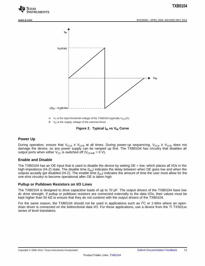
IIN
VIN
VT/4 k
–(VD – VT)/4 k
A. VT is the input threshold voltage of the TXB0104 (typically VCCI/2).B. VD is the supply voltage of the external driver.
TXB0104
www.ti.com SCES650F –APRIL 2006–REVISED MAY 2012
Figure 2. Typical IIN vs VIN Curve
Power Up
During operation, ensure that VCCA ≤ VCCB at all times. During power-up sequencing, VCCA ≥ VCCB does notdamage the device, so any power supply can be ramped up first. The TXB0104 has circuitry that disables alloutput ports when either VCC is switched off (VCCA/B = 0 V).
Enable and Disable
The TXB0104 has an OE input that is used to disable the device by setting OE = low, which places all I/Os in thehigh-impedance (Hi-Z) state. The disable time (tdis) indicates the delay between when OE goes low and when theoutputs acutally get disabled (Hi-Z). The enable time (ten) indicates the amount of time the user must allow for theone-shot circuitry to become operational after OE is taken high.
Pullup or Pulldown Resistors on I/O Lines
The TXB0104 is designed to drive capacitive loads of up to 70 pF. The output drivers of the TXB0104 have lowdc drive strength. If pullup or pulldown resistors are connected externally to the data I/Os, their values must bekept higher than 50 kΩ to ensure that they do not contend with the output drivers of the TXB0104.
For the same reason, the TXB0104 should not be used in applications such as I2C or 1-Wire where an open-drain driver is connected on the bidirectional data I/O. For these applications, use a device from the TI TXS01xxseries of level translators.
Copyright © 2006–2012, Texas Instruments Incorporated Submit Documentation Feedback 11
Product Folder Links: TXB0104

From Output Under Test
LOAD CIRCUIT FORENABLE/DISABLE
TIME MEASUREMENT
S1
2 × VCCO
Open
50 k
VCCI
0 V
VCCI/2 VCCI/2
tw
VOLTAGE WAVEFORMSPROPAGATION DELAY TIMES
VOLTAGE WAVEFORMSPULSE DURATION
Input
tPZL/tPLZtPHZ/tPZH
2 × VCCOOpen
TEST S1
A. CL includes probe and jig capacitance.B. All input pulses are supplied by generators having the following characteristics: PRR10 MHz, ZO = 50 Ω, dv/dt ≥ 1 V/ns.C. The outputs are measured one at a time, with one transition per measurement.D. tPLH and tPHL are the same as tpd.E. VCCI is the VCC associated with the input port.F. VCCO is the VCC associated with the output port.G. All parameters and waveforms are not applicable to all devices.
50 kFrom Output
Under Test
1 M15 pF 15 pF
LOAD CIRCUIT FOR MAX DATA RATE,PULSE DURATION PROPAGATION
DELAY OUTPUT RISE AND FALL TIMEMEASUREMENT
tPLH tPHL
0 V
VCCO/2
VCCI/2 VCCI/2
0.9 VCCOVCCO/2
tr
0.1 VCCO
tf
VCCIInput
OutputVOH
VOL
TXB0104
SCES650F –APRIL 2006–REVISED MAY 2012 www.ti.com
PARAMETER MEASUREMENT INFORMATION
Figure 3. Load Circuits and Voltage Waveforms
12 Submit Documentation Feedback Copyright © 2006–2012, Texas Instruments Incorporated
Product Folder Links: TXB0104
TXB0104
www.ti.com SCES650F –APRIL 2006–REVISED MAY 2012
REVISION HISTORY
Changes from Revision E (February 2010) to Revision F Page
• Added notes to pin out graphics. .......................................................................................................................................... 1
Copyright © 2006–2012, Texas Instruments Incorporated Submit Documentation Feedback 13
Product Folder Links: TXB0104
PACKAGE OPTION ADDENDUM
www.ti.com 16-Aug-2013
Addendum-Page 1
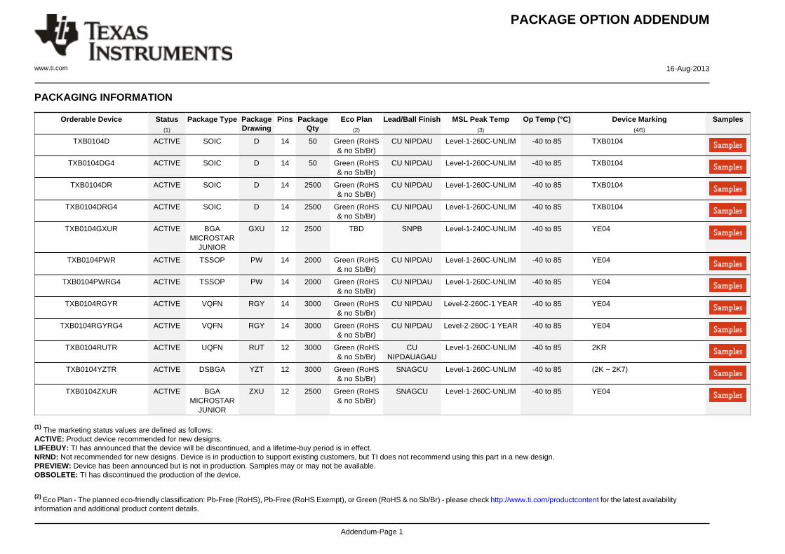
PACKAGING INFORMATION
Orderable Device Status(1)
Package Type PackageDrawing
Pins PackageQty
Eco Plan(2)
Lead/Ball Finish MSL Peak Temp(3)
Op Temp (°C) Device Marking(4/5)
Samples
TXB0104D ACTIVE SOIC D 14 50 Green (RoHS& no Sb/Br)
CU NIPDAU Level-1-260C-UNLIM -40 to 85 TXB0104
TXB0104DG4 ACTIVE SOIC D 14 50 Green (RoHS& no Sb/Br)
CU NIPDAU Level-1-260C-UNLIM -40 to 85 TXB0104
TXB0104DR ACTIVE SOIC D 14 2500 Green (RoHS& no Sb/Br)
CU NIPDAU Level-1-260C-UNLIM -40 to 85 TXB0104
TXB0104DRG4 ACTIVE SOIC D 14 2500 Green (RoHS& no Sb/Br)
CU NIPDAU Level-1-260C-UNLIM -40 to 85 TXB0104
TXB0104GXUR ACTIVE BGAMICROSTAR
JUNIOR
GXU 12 2500 TBD SNPB Level-1-240C-UNLIM -40 to 85 YE04
TXB0104PWR ACTIVE TSSOP PW 14 2000 Green (RoHS& no Sb/Br)
CU NIPDAU Level-1-260C-UNLIM -40 to 85 YE04
TXB0104PWRG4 ACTIVE TSSOP PW 14 2000 Green (RoHS& no Sb/Br)
CU NIPDAU Level-1-260C-UNLIM -40 to 85 YE04
TXB0104RGYR ACTIVE VQFN RGY 14 3000 Green (RoHS& no Sb/Br)
CU NIPDAU Level-2-260C-1 YEAR -40 to 85 YE04
TXB0104RGYRG4 ACTIVE VQFN RGY 14 3000 Green (RoHS& no Sb/Br)
CU NIPDAU Level-2-260C-1 YEAR -40 to 85 YE04
TXB0104RUTR ACTIVE UQFN RUT 12 3000 Green (RoHS& no Sb/Br)
CUNIPDAUAGAU
Level-1-260C-UNLIM -40 to 85 2KR
TXB0104YZTR ACTIVE DSBGA YZT 12 3000 Green (RoHS& no Sb/Br)
SNAGCU Level-1-260C-UNLIM -40 to 85 (2K ~ 2K7)
TXB0104ZXUR ACTIVE BGAMICROSTAR
JUNIOR
ZXU 12 2500 Green (RoHS& no Sb/Br)
SNAGCU Level-1-260C-UNLIM -40 to 85 YE04
(1) The marketing status values are defined as follows:ACTIVE: Product device recommended for new designs.LIFEBUY: TI has announced that the device will be discontinued, and a lifetime-buy period is in effect.NRND: Not recommended for new designs. Device is in production to support existing customers, but TI does not recommend using this part in a new design.PREVIEW: Device has been announced but is not in production. Samples may or may not be available.OBSOLETE: TI has discontinued the production of the device.
(2) Eco Plan - The planned eco-friendly classification: Pb-Free (RoHS), Pb-Free (RoHS Exempt), or Green (RoHS & no Sb/Br) - please check http://www.ti.com/productcontent for the latest availabilityinformation and additional product content details.
PACKAGE OPTION ADDENDUM
www.ti.com 16-Aug-2013
Addendum-Page 2
TBD: The Pb-Free/Green conversion plan has not been defined.Pb-Free (RoHS): TI's terms "Lead-Free" or "Pb-Free" mean semiconductor products that are compatible with the current RoHS requirements for all 6 substances, including the requirement thatlead not exceed 0.1% by weight in homogeneous materials. Where designed to be soldered at high temperatures, TI Pb-Free products are suitable for use in specified lead-free processes.Pb-Free (RoHS Exempt): This component has a RoHS exemption for either 1) lead-based flip-chip solder bumps used between the die and package, or 2) lead-based die adhesive used betweenthe die and leadframe. The component is otherwise considered Pb-Free (RoHS compatible) as defined above.Green (RoHS & no Sb/Br): TI defines "Green" to mean Pb-Free (RoHS compatible), and free of Bromine (Br) and Antimony (Sb) based flame retardants (Br or Sb do not exceed 0.1% by weightin homogeneous material)
(3) MSL, Peak Temp. -- The Moisture Sensitivity Level rating according to the JEDEC industry standard classifications, and peak solder temperature.
(4) There may be additional marking, which relates to the logo, the lot trace code information, or the environmental category on the device.
(5) Multiple Device Markings will be inside parentheses. Only one Device Marking contained in parentheses and separated by a "~" will appear on a device. If a line is indented then it is a continuationof the previous line and the two combined represent the entire Device Marking for that device.
Important Information and Disclaimer:The information provided on this page represents TI's knowledge and belief as of the date that it is provided. TI bases its knowledge and belief on informationprovided by third parties, and makes no representation or warranty as to the accuracy of such information. Efforts are underway to better integrate information from third parties. TI has taken andcontinues to take reasonable steps to provide representative and accurate information but may not have conducted destructive testing or chemical analysis on incoming materials and chemicals.TI and TI suppliers consider certain information to be proprietary, and thus CAS numbers and other limited information may not be available for release.
In no event shall TI's liability arising out of such information exceed the total purchase price of the TI part(s) at issue in this document sold by TI to Customer on an annual basis.
OTHER QUALIFIED VERSIONS OF TXB0104 :
• Automotive: TXB0104-Q1
NOTE: Qualified Version Definitions:
• Automotive - Q100 devices qualified for high-reliability automotive applications targeting zero defects
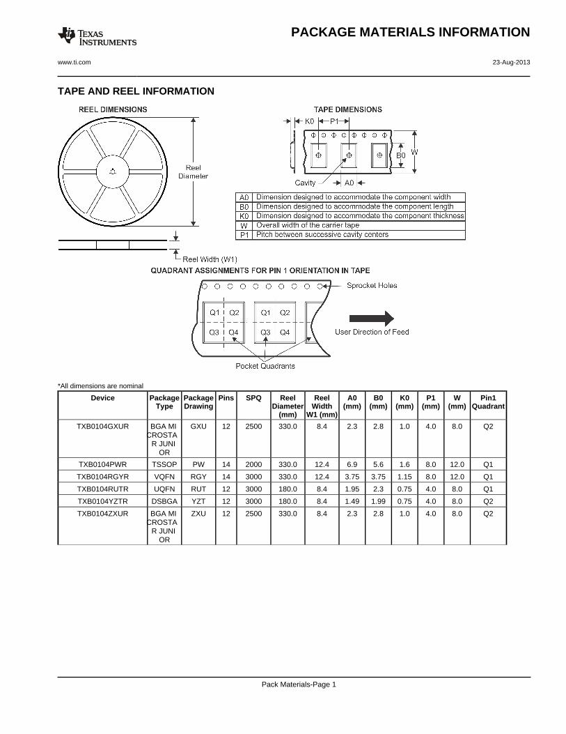
TAPE AND REEL INFORMATION
*All dimensions are nominal
Device PackageType
PackageDrawing
Pins SPQ ReelDiameter
(mm)
ReelWidth
W1 (mm)
A0(mm)
B0(mm)
K0(mm)
P1(mm)
W(mm)
Pin1Quadrant
TXB0104GXUR BGA MI CROSTA
R JUNI OR
GXU 12 2500 330.0 8.4 2.3 2.8 1.0 4.0 8.0 Q2
TXB0104PWR TSSOP PW 14 2000 330.0 12.4 6.9 5.6 1.6 8.0 12.0 Q1
TXB0104RGYR VQFN RGY 14 3000 330.0 12.4 3.75 3.75 1.15 8.0 12.0 Q1
TXB0104RUTR UQFN RUT 12 3000 180.0 8.4 1.95 2.3 0.75 4.0 8.0 Q1
TXB0104YZTR DSBGA YZT 12 3000 180.0 8.4 1.49 1.99 0.75 4.0 8.0 Q2
TXB0104ZXUR BGA MI CROSTA
R JUNI OR
ZXU 12 2500 330.0 8.4 2.3 2.8 1.0 4.0 8.0 Q2
PACKAGE MATERIALS INFORMATION
www.ti.com 23-Aug-2013
Pack Materials-Page 1

*All dimensions are nominal
Device Package Type Package Drawing Pins SPQ Length (mm) Width (mm) Height (mm)
TXB0104GXUR BGA MICROSTARJUNIOR
GXU 12 2500 338.1 338.1 20.6
TXB0104PWR TSSOP PW 14 2000 367.0 367.0 35.0
TXB0104RGYR VQFN RGY 14 3000 367.0 367.0 35.0
TXB0104RUTR UQFN RUT 12 3000 202.0 201.0 28.0
TXB0104YZTR DSBGA YZT 12 3000 182.0 182.0 17.0
TXB0104ZXUR BGA MICROSTARJUNIOR
ZXU 12 2500 338.1 338.1 20.6
PACKAGE MATERIALS INFORMATION
www.ti.com 23-Aug-2013
Pack Materials-Page 2


IMPORTANT NOTICE
Texas Instruments Incorporated and its subsidiaries (TI) reserve the right to make corrections, enhancements, improvements and otherchanges to its semiconductor products and services per JESD46, latest issue, and to discontinue any product or service per JESD48, latestissue. Buyers should obtain the latest relevant information before placing orders and should verify that such information is current andcomplete. All semiconductor products (also referred to herein as “components”) are sold subject to TI’s terms and conditions of salesupplied at the time of order acknowledgment.
TI warrants performance of its components to the specifications applicable at the time of sale, in accordance with the warranty in TI’s termsand conditions of sale of semiconductor products. Testing and other quality control techniques are used to the extent TI deems necessaryto support this warranty. Except where mandated by applicable law, testing of all parameters of each component is not necessarilyperformed.
TI assumes no liability for applications assistance or the design of Buyers’ products. Buyers are responsible for their products andapplications using TI components. To minimize the risks associated with Buyers’ products and applications, Buyers should provideadequate design and operating safeguards.
TI does not warrant or represent that any license, either express or implied, is granted under any patent right, copyright, mask work right, orother intellectual property right relating to any combination, machine, or process in which TI components or services are used. Informationpublished by TI regarding third-party products or services does not constitute a license to use such products or services or a warranty orendorsement thereof. Use of such information may require a license from a third party under the patents or other intellectual property of thethird party, or a license from TI under the patents or other intellectual property of TI.
Reproduction of significant portions of TI information in TI data books or data sheets is permissible only if reproduction is without alterationand is accompanied by all associated warranties, conditions, limitations, and notices. TI is not responsible or liable for such altereddocumentation. Information of third parties may be subject to additional restrictions.
Resale of TI components or services with statements different from or beyond the parameters stated by TI for that component or servicevoids all express and any implied warranties for the associated TI component or service and is an unfair and deceptive business practice.TI is not responsible or liable for any such statements.
Buyer acknowledges and agrees that it is solely responsible for compliance with all legal, regulatory and safety-related requirementsconcerning its products, and any use of TI components in its applications, notwithstanding any applications-related information or supportthat may be provided by TI. Buyer represents and agrees that it has all the necessary expertise to create and implement safeguards whichanticipate dangerous consequences of failures, monitor failures and their consequences, lessen the likelihood of failures that might causeharm and take appropriate remedial actions. Buyer will fully indemnify TI and its representatives against any damages arising out of the useof any TI components in safety-critical applications.
In some cases, TI components may be promoted specifically to facilitate safety-related applications. With such components, TI’s goal is tohelp enable customers to design and create their own end-product solutions that meet applicable functional safety standards andrequirements. Nonetheless, such components are subject to these terms.
No TI components are authorized for use in FDA Class III (or similar life-critical medical equipment) unless authorized officers of the partieshave executed a special agreement specifically governing such use.
Only those TI components which TI has specifically designated as military grade or “enhanced plastic” are designed and intended for use inmilitary/aerospace applications or environments. Buyer acknowledges and agrees that any military or aerospace use of TI componentswhich have not been so designated is solely at the Buyer's risk, and that Buyer is solely responsible for compliance with all legal andregulatory requirements in connection with such use.
TI has specifically designated certain components as meeting ISO/TS16949 requirements, mainly for automotive use. In any case of use ofnon-designated products, TI will not be responsible for any failure to meet ISO/TS16949.
Products Applications
Audio www.ti.com/audio Automotive and Transportation www.ti.com/automotive
Amplifiers amplifier.ti.com Communications and Telecom www.ti.com/communications
Data Converters dataconverter.ti.com Computers and Peripherals www.ti.com/computers
DLP® Products www.dlp.com Consumer Electronics www.ti.com/consumer-apps
DSP dsp.ti.com Energy and Lighting www.ti.com/energy
Clocks and Timers www.ti.com/clocks Industrial www.ti.com/industrial
Interface interface.ti.com Medical www.ti.com/medical
Logic logic.ti.com Security www.ti.com/security
Power Mgmt power.ti.com Space, Avionics and Defense www.ti.com/space-avionics-defense
Microcontrollers microcontroller.ti.com Video and Imaging www.ti.com/video
RFID www.ti-rfid.com
OMAP Applications Processors www.ti.com/omap TI E2E Community e2e.ti.com
Wireless Connectivity www.ti.com/wirelessconnectivity
Mailing Address: Texas Instruments, Post Office Box 655303, Dallas, Texas 75265Copyright © 2013, Texas Instruments Incorporated