Embed Size (px)
Citation preview

DEEP SUBMICRON CMOS DESIGN 4. The inverter
1 E.Sicard, S. Delmas-Bendhia 03/04/03
4 The
Inverter
1. Introduction
The inverter is probably the most important basic logic cell in circuit design. Two logic symbol are often used to
represent the inverter: the "old style" inverter (Left of figure 4-1), and the IEEE symbol (right of figure 4-1). In
DSCH, we preferably use traditional symbol layout. As the logic truth table of figure 4-1 shows, the cell inverts the
logic value of the input In into an output Out.
In Out
0 1
1 0
X X
Fig. 4-1: Symbols used to represent the logic inverter
In the truth table, the symbol 0 represents 0.0V while 1 represents the logic supply, which is 1.2V in 0.12µm. The
symbol X means "undefined". This state is equivalent to an undefined voltage, as for a floating input node without any
input connection. The undefined state appears in gray in the simulations and chronograms.
2. CMOS Inverter

DEEP SUBMICRON CMOS DESIGN 4. The inverter
2 E.Sicard, S. Delmas-Bendhia 03/04/03
The CMOS inverter design is detailed in the figure 4-2. Here one p-channel MOS and one n-channel MOS transistors
are used as switches. Notice that the size of each device is plotted (W accounts for the width, L for the length). The
channel width for pMOS devices is set to twice the channel width for nMOS devices. The reason is described in
details in the next chapters.
Fig. 4-2: The CMOS inverter is based on one n-channel and one p-channel MOS devices
Fig. 4-3: Logic simulation of the CMOS inverter (CmosInv.sch)
When the input signal is logic 0 (Fig. 4-3 left), the nMOS is switched off while the PMOS passes VDD through the
output, which turns to 1. When the input signal is logic 1 (Fig. 4-3 b), the pMOS is switched off while the nMOS
passes VSS to the output, which goes back to 0. In that simulation, the MOS is considered as a simple switch. The n-
channel MOS symbol is a device that allows the current to flow between the source and the drain when the gate
voltage is "1".
To simulate the inverter at logic level, start the software DSCH2, load the file “CmosInv.SCH”, and launch the
simulation by the command Simulate ? Start Simulate. Click inside the button in1. The result is displayed on the
output out1. The red value indicates logic 1, the black value means a logic 0. Click the button “Stop simulation" of the

DEEP SUBMICRON CMOS DESIGN 4. The inverter
3 E.Sicard, S. Delmas-Bendhia 03/04/03
simulation menu to return to the schematic editor. Click the "chronogram" icon to get access to the chronograms of
the previous simulation (Figure 4-4). As seen in the waveform, the output is the logic opposite of the input.
Fig. 4-4 Chronograms of the inverter simulation (CmosInv.SCH)
3. Inverter Layout
In this paragraph, details on the layout of a CMOS inverter are provided. The simplest way to create a CMOS
inverter is to generate both n-channel MOS an p-channel MOS devices using the cell generator provided by
Microwind. The advantage of this approach is to avoid any design rule error. The corresponding menu is reported
below. You can generate a n-channel or p-channel device. A double gate device may also be created for EEPROM
memory devices (See chapter 10). By default the proposed length is the minimum length available in the technology
(2 lambda), and the width is 10 lambda. In 0.12µm technology, where lambda is 0.06µm, the corresponding size is
0.12µm for the length and 0.6µm for the width.
Fig. 4-5 Using the MOS generator to add n-channel and p-channel MOS devices on the layout

DEEP SUBMICRON CMOS DESIGN 4. The inverter
4 E.Sicard, S. Delmas-Bendhia 03/04/03
Pmos width Pmos length
Nmos width Nmos length
Double pmos width
Nmos width
Fig. 4-6 The layout of one nMOS and one pMOS to build the CMOS inverter (invSizing.MSK)
The design starts with the implementation of one nMOS and one pMOS, as shown in figure 4-6. Using the same
default channel width (0.6µm in CMOS 0.12µm) for nMOS and pMOS is not the best idea, as the p-channel MOS
switches half the current of the n-channel MOS. The origin of this mismatch can be seen in the general expression
of the current delivered by n-channel MOS devices (equation 4-1) and p-channel MOS devices (equation 4-2).
Vb)Vs,Vg,f(Vd,LW
TOXµ
ee Ids(Nmos)Nmos
Nmosnr0? (Equ. 4-1)
)VbVs,Vg,f(Vd,LW
TOXµ
ee Ids(Pmos)Pmos
Pmospr0? (Equ. 4-2)
If Wnmos=Wpmos and Lnmos=Lpmos, Ids(Nmos) is proportional to µn while Ids(Pmos) is proportional to µp.
Typical mobility values are:
svmn ./068.0 2?? for electrons
svmp ./025.0 2?? for holes
Consequently, the current delivered by the n-channel MOS device is more than twice the one of the p-channel MOS.
Usually, the inverter is designed with balanced currents to avoid significant switching discrepancies. In other words,
switching from 0 to 1 should take approximately the same time as switching from 1 to 0. Therefore, balanced
current performances are required.
DEEP SUBMICRON CMOS DESIGN 4. The inverter
5 E.Sicard, S. Delmas-Bendhia 03/04/03
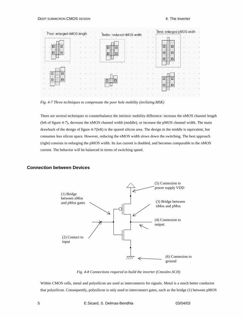
Fig. 4-7 Three techniques to compensate the poor hole mobility (invSizing.MSK)
There are several techniques to counterbalance the intrinsic mobility difference: increase the nMOS channel length
(left of figure 4-7), decrease the nMOS channel width (middle), or increase the pMOS channel width. The main
drawback of the design of figure 4-7(left) is the spared silicon area. The design in the middle is equivalent, but
consumes less silicon space. However, reducing the nMOS width slows down the switching. The best approach
(right) consists in enlarging the pMOS width. Its Ion current is doubled, and becomes comparable to the nMOS
current. The behavior will be balanced in terms of switching speed.
Connection between Devices
(1) Bridge between nMos and pMos gates
(2) Contact to input
(5) Connexion to power supply VDD
(6) Connexion to ground
(4) Connexion to output
(3) Bridge between nMos and pMos
Fig. 4-8 Connections required to build the inverter (CmosInv.SCH)
Within CMOS cells, metal and polysilicon are used as interconnects for signals. Metal is a much better conductor
that polysilicon. Consequently, polysilicon is only used to interconnect gates, such as the bridge (1) between pMOS

DEEP SUBMICRON CMOS DESIGN 4. The inverter
6 E.Sicard, S. Delmas-Bendhia 03/04/03
and nMOS gates, as described in the schematic diagram of figure 4-8. Polysilicon is rarely used for long
interconnects, except if a huge resistance value is expected.
In the layout shown in figure 4-9, the polysilicon bridge links the gate of the n-channel MOS with the gate of the p-
channel MOS device. The polysilicon serves as the gate control and the bridge between MOS gates.
(1) Polysilicon Bridge between pMOS and nMOS gates
2 lambda polysilicon gate size to achieve fastest switching
Fig. 4-9 Polysilicon bridge between nMOS and pMOS devices (InvSteps.MSK)
Useful Editing Tools
The following commands may help you in the layout design and verification processes.
Command Icon/Short cut Menu Description UNDO CTRL+U Edit menu Cancel the last editing operation DELETE
CTRL+X
Edit menu Erase some layout included in the given area or pointed by the mouse.
STRETCH
Edit menu Changes the size of one box, or moves the layout included in the given area.
COPY
CTRL+C
Edit Menu Copy of the layout included in the given area.
VIEW ELECTRICAL NODE
CTRL+N
View Menu Verifies the electrical net connections.
2D CROSS-SECTION
Simulate Menu Shows the aspect of the circuit in vertical cross-section.
Table 4-1: A set of useful editing tools

DEEP SUBMICRON CMOS DESIGN 4. The inverter
7 E.Sicard, S. Delmas-Bendhia 03/04/03
Metal-to-poly
As polysilicon is a poor conductor, metal is preferred to interconnect signals and supplies. Consequently, the input
connection of the inverter is made with metal. Metal and polysilicon are separated by an oxide which prevents from
electrical connection. Therefore, a box of metal drawn across a box of polysilicon do not make an electrical
connection (Figure 4-10). To build an electrical connection, a physical contact is needed. The corresponding layer is
called "contact". You may insert a metal-to-polysilicon contact in the layout using a direct macro situated in the
palette.
Polysilicon (2 ? min)
Metal (4 ? min) Contact (2x2 ? )
Enlarged poly area (4x4 ? )
Fig. 4-10 Physical contact between metal and polysilicon
(2) Contact between polysilicon and the input Polysilicon box between
the contact and the gate
Fig. 4-11 Physical contact between metal and polysilicon (InvSteps.MSK)

DEEP SUBMICRON CMOS DESIGN 4. The inverter
8 E.Sicard, S. Delmas-Bendhia 03/04/03
Metal extension for future interconnection
Metal bridge between nMOS and pMOS gates drains
Fig. 4-12 Adding a poly contact, poly and metal bridges to construct the CMOS inverter (InvSteps.MSK)
The Process Simulator shows the vertical aspect of the layout, as when fabrication has been completed. This feature
is a significant aid to understand the circuit structure and the way layers are stacked on the top of each other. A click
of the mouse at the left side of the n-channel device layout and the release of the mouse at the right side give the
cross-section reported in figure 4-13.
Drain (N+ diffusion)
Source (N+ diffusion)
Thick oxide (SiO2)
NMOS gate (Polysilicon)
Metal 1
Ground polarization
Fig.4-13 The 2D process section of the inverter circuit near the nMOS device (InvSteps.MSK)
Supply Connections

DEEP SUBMICRON CMOS DESIGN 4. The inverter
9 E.Sicard, S. Delmas-Bendhia 03/04/03
The next design step consists in adding supply connections, that is the positive supply VDD and the ground supply
VSS. In figure 4-14, we use the metal2 layer (Second level of metallization) to create horizontal supply connections.
Notice that the metal connections have a large width. This is because a strong current may flow within these supply
interconnects. Enlarging the supply metal lines reduces the resistance and avoids electrical overstress called
electromigration (More details are given in chapter 5 dedicated to interconnects).
VDD supply rail in metal2
Metal 2 over metal
VSS supply rail in metal2
Metal 2 over metal
Fig.4-14 Adding metal2 supply lines and the appropriate vias (InvSteps.MSK)
Metal/Metal2 contact
Fig.4-15 The metal/Metal2 contact in the palette
The metal layers are electrically isolated by a SiO2 dielectric. Consequently, the metal2 supply line floats over the
inverter cell and no physical connection exist down to the MOS source region. The simplest way to build the physical
connection is to add a metal/Metal2 contact that may be found in the palette (Figure 4-15).

DEEP SUBMICRON CMOS DESIGN 4. The inverter
10 E.Sicard, S. Delmas-Bendhia 03/04/03
Metal2 is physically isolated from metal1 by silicon oxide The via plug
connects metal2 to metal1 to build the connection from VSS to the nMOS source
VSS supply line VSS supply line
NMOS NMOS
Fig.4-16 2-D view of the connection built near the nMOS region to connect the source to the VSS supply line
As seen in figure 4-16, the connection is created by a plug called "via" between metal2 and metal layers.
The final layout design step consists in adding polarization contacts. These contacts convey the VSS and VDD voltage
supply close to the bulk regions of the device. We have seen that the MOS behavior is influenced by the bulk
polarization (See equations 3-xxx and characteristics such as in figure 3-xxx). If we ensure a clean supply polarization
near each device (VSS for nMOS, VDD for pMOS), we avoid such variations. Remember that the n-well region
should always be polarized to a high voltage to avoid short-circuit between VDD and VSS.
DEEP SUBMICRON CMOS DESIGN 4. The inverter
11 E.Sicard, S. Delmas-Bendhia 03/04/03
P+/Pwell contact and bridge to VSS
N+/Nwell contact and bridge to VDD
Via to connect metal2 and metal 1
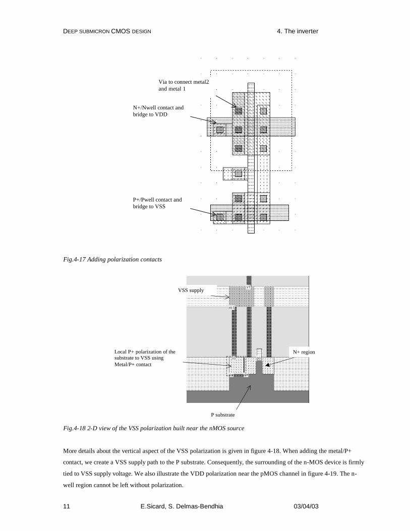
Fig.4-17 Adding polarization contacts
VSS supply
Local P+ polarization of the substrate to VSS using Metal/P+ contact
P substrate
N+ region
Fig.4-18 2-D view of the VSS polarization built near the nMOS source
More details about the vertical aspect of the VSS polarization is given in figure 4-18. When adding the metal/P+
contact, we create a VSS supply path to the P substrate. Consequently, the surrounding of the n-MOS device is firmly
tied to VSS supply voltage. We also illustrate the VDD polarization near the pMOS channel in figure 4-19. The n-
well region cannot be left without polarization.

DEEP SUBMICRON CMOS DESIGN 4. The inverter
12 E.Sicard, S. Delmas-Bendhia 03/04/03
P substrate
N-well polarized to VDD thanks to metal/N+ contact
N+ diffusion
VDD supply
Without polarization -(forbidden)
With polarization (Obligatory)
Possible parasitic path from VDD to VSS when N-well is floating
Fig.4-19 2-D view of the VDD polarization built near the pMOS source
Adding the VDD polarization in the n-well region is a very strict rule. The local polarization built with a metal/N+
diffusion contact, as shown in figure 4-19, is efficient to avoid a floating n-well region, which may result in parasitic
current path from the PMOS source down to the P substrate usually tied to VSS. The current path may be strong
enough to damage the chip. This effect is called latchup <Gloss>.
Process steps to build the Inverter
At that point, it might be interesting to illustrate the steps of fabrication as it would sequenced in a foundry.
Microwind includes a 3D process viewer for that purpose. Click Simulate? Process steps in 3D. The simulation of
the CMOS fabrication process is performed, step by step by a click on Next Step. On figure 4-20, the picture on the
left represents the nMOS device, pMOS device, common polysilicon gate and contacts. The picture on the right
represents the same portion of layout with the metal layers stacked on the top of the active devices.

DEEP SUBMICRON CMOS DESIGN 4. The inverter
13 E.Sicard, S. Delmas-Bendhia 03/04/03
Fig.4-20 The step-by-step fabrication of the Inverter circuit (InvSteps.MSK)
4. Inverter Simulation
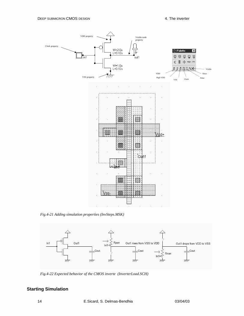
The inverter simulation is conducted as follows. Firstly, a VDD supply source (1.2V) is fixed to the upper metal2
supply line, and a VSS supply source (0.0V) is fixed to the lower metal2 supply line. The properties are located in
the palette menu. Simply click the desired property , and click on the desired location in the layout. Add a clock on
the inverter input node (The default node name clock1 has been changed into Vin)and a visible property on the
output node (The default name out1 has been changed into Vout).
The expected behavior is shown in figure 4-22. The basic phenomenon is the charge and discharge of the output
parasitic capacitor Cout, which is the sum of junction and wire capacitance. When In1 is equal to 0, the pMOS
device is on, and the capacitor Cout is charged until its voltage rises to VDD. When In1 is equal to 1, the nMOS
device is on, and the capacitor Cout is discharged until its voltage reaches VSS.
DEEP SUBMICRON CMOS DESIGN 4. The inverter
14 E.Sicard, S. Delmas-Bendhia 03/04/03
Clock property
VSS property
VDD property Visible nodeproperty
VDD
High VDDVSS Clock Pulse
Sinus
Visible
Fig.4-21 Adding simulation properties (InvSteps.MSK)
Fig.4-22 Expected behavior of the CMOS inverte (InverterLoad.SCH)
Starting Simulation

DEEP SUBMICRON CMOS DESIGN 4. The inverter
15 E.Sicard, S. Delmas-Bendhia 03/04/03
The command Simulate ? Run Simulation gives access to four simulations modes: the Voltage vs. time, voltage and
current vcs. Time, the static transfer function (Voltage vs. voltage) and the frequency versus time. All these
simulation modes are applicable to the inverter simulation.
Fig.4-23 The four simulation modes in Microwind
Due to the fact that the layout InvSteps.MSK not only includes the inverter correctly polarized, but also several other
mos devices without any simulation properties, a warning window appears prior to the analog simulation, as shown in
figure 4-24. In this case, you may click Simulate as it. In normal cases, all n-well regions should be stuck at VDD.
Fig.4-24 Missing polarization in n-well regions provoke a warning prior to simulation (InvSteps.MSK)
Voltage vs. Time
Select the simulation mode Voltage vs. Time. The analog simulation of the circuit is performed. The time domain
waveform, proposed by default, details the evolution of the voltages in1 and out1 versus time. This mode is also
called transient simulation, as shown in figure 4-25.

DEEP SUBMICRON CMOS DESIGN 4. The inverter
16 E.Sicard, S. Delmas-Bendhia 03/04/03
Fig.4-25 Transient simulation of the CMOS inverter (InvSteps.MSK)
The truth-table is verified as follows. A logic zero corresponds to a zero voltage and a logic 1 to a 1.20V. When the
input rises to 1, the output falls to 0, with a 6 Pico-second delay (6.10-12 second).
In Out In (V) Out (V)
0 1 0.0 1.2
1 0 1.2 0.0 Logic table Analog voltage table
Current vs. Time
The inverter consumes power during transitions, due to two separate effects. The first is short circuit power arising
from momentary short-circuit current that flow from VDD to VSS when the transistor functions in the incomplete-
on/off state (Figure 4-26). The second is the charging/discharging power, which depends on the output wire
capacitance. With small loading, the short circuit power loss is dominant. With a huge loading, that is a large output
node capacitance, the loading power is dominant.

DEEP SUBMICRON CMOS DESIGN 4. The inverter
17 E.Sicard, S. Delmas-Bendhia 03/04/03
Short circuit current
Charge/Discharge current
Fig. 4-26: Short circuit current in CMOS inverters (InverterLoad.SCH)
The power consumption occurs briefly during transitions of the output, either from 0 to 1 or from 1 to 0 (Fig. 4-27).
The simulation contains the supply currents in the upper window, and all voltage waveforms in the lower window.
The current consumption is important only during a very short period corresponding to the charge or discharge of
the output node. Without any switching activity, the current is almost equal to zero.
Fig. 4-27: Simulation of the current peaks appearing between VDD and VSS in the CMOS inverter at each output
transition (InvSteps.MSK)
Inverter Delay
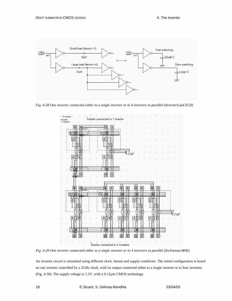
As the number of gates connected to the inverter output node increase, the load capacitance increases. The fanout
<glossary> corresponds to the number of gates connected to the cell output. Physically, a large fanout means a large
number of connections (Figure 4-28), that is a large load capacitance.
DEEP SUBMICRON CMOS DESIGN 4. The inverter
18 E.Sicard, S. Delmas-Bendhia 03/04/03
Fig. 4-28 One inverter connected either to a single inverter or to 4 inverters in parallel (InverterLoad.SCH)
Fig. 4-29 One inverter connected either to a single inverter or to 4 inverters in parallel (InvFanout.MSK)
An inverter circuit is simulated using different clock, fanout and supply conditions. The initial configuration is based
on one inverter controlled by a 2GHz clock, with its output connected either to a single inverter or to four inverters
(Fig. 4-30). The supply voltage is 1.2V, with a 0.12µm CMOS technology.

DEEP SUBMICRON CMOS DESIGN 4. The inverter
19 E.Sicard, S. Delmas-Bendhia 03/04/03
Clock switching
Fanout 1
Fanout 4
Fig. 4-30: Influence of the output capacitance on the current and switching response (InvFanout.MSK)
Now, we connect 4 inverter circuits to the output node, thus increasing the charge capacitance. In the simulation
chronograms reported in figure 4-30, the inverter delay is significantly increased. When we investigate the delay
variation with the output capacitance load, we observe the curve reported in figure 4-31. It can be seen that the gate
delay variation with the loading capacitance is quite linear. A 100fF load leads to around 300ps delay in CMOS
0.12µm technology.
Fig. 4-31: Inverter delay increase with the output capacitance (InvCapa.MSK)

DEEP SUBMICRON CMOS DESIGN 4. The inverter
20 E.Sicard, S. Delmas-Bendhia 03/04/03
In Microwind2, we may obtain directly this type of screen thanks to the command Parametric Analysis. Load the file
InvCapa.MSK, invoke the command Parametric Analysis, click in the output node, and click Start Analysis. By
default, the capacitance of the output node is increased step by step from its default value Cdef to Cdef+100fF. For each
value of the output capacitance, the analog simulation is performed, and the last computed rise time is plotted,
appearing as one single red dot in the graphs. The complete graph is built once all analog simulation have been
completed. The memory button enables to store one curve (rise time evaluation for example) prior to a new parametric
simulation, for comparison purpose. Three main parameters may vary in the parametric analysis: the capacitance as in
figure 4-31, voltage, or temperature. Several analog parameters may be monitored: rise and fall delay, oscillating
frequency, power consumption, final voltage of a node, crosstalk, etc..
5. Power Consumption
The power consumption P is computed by Microwind as the average product of the supply voltage VDD and the
supply current IDD, computed at each iteration step. In other words:
stepsVI
P DDDD??.
(Equ. 4-3)
Three main factors contribute to the power consumption P: the load capacitance C, the supply voltage VDD and the
clock frequency f. For a CMOS inverter, this relation is usually represented by the first-order approximation below.
The equation 4-4 shows a linear dependence of the power consumption P with the total capacitance C and the
operating frequency f. The power consumption is also proportional to the square of the supply voltage VDD.
fC V P DD2.
21 ?? (Equ. 4-4)
Where:
k: technological factor (close from 1)
C: Output load capacitance (Farad)
VDD: supply voltage (V)
f: Clock frequency (Hz)
? : switching activity factor (Between 0 and 1)
Frequency dependence
We can verify the linear dependence of the power consumption with the operating frequency by simulating a CMOS
inverter circuit. At each time-domain analog simulation, we get a value of the power consumption, which is computed
by Microwind as the average product of the supply voltage VDD and the supply current IDD (Equation 4-3).

DEEP SUBMICRON CMOS DESIGN 4. The inverter
21 E.Sicard, S. Delmas-Bendhia 03/04/03
Fig. 4-32: CMOS inverter setup used to simulate of the effect of the clock frequency on the power consumption. A
10fF load is added on the output to represent a typical loading condition in 0.12µm (CmosLoad.MSK)
In the case of figure 4-32, a 1GHz switching of the inverter induces a circuit power dissipation of 15.7µW. When we
change the frequency, we observe linear increase of P with the clock frequency, as forecast in equation 4-4 (Figure 4-
33).

DEEP SUBMICRON CMOS DESIGN 4. The inverter
22 E.Sicard, S. Delmas-Bendhia 03/04/03
1.00.5 1.5
Clock frequency(GHz)
Inverter consumption (µW)
10.0
20.0
30.0
0.00.0
Slope 15.7µW/GHz23.5
7.8
15.7
Fig. 4-33: Power consumption increase with the clock frequency, for an inverter with a 10fF load, in CMOS 0.12µm
(CmosLoad.MSK)
As the power consumption is linearly proportional to the clock frequency, a usual metric found in most cell libraries is
the µW/GHz. In the case of the simple inverter and its 10fF load, we get 15.7µW/GHz.
Supply Voltage dependence It can be considered, as a first-order approximation that the average power consumption is proportional to VDD2
(Equation 4-4). We use the parametric analysis tool in Microwind to control the incremental change of the supply
voltage, from 0.5 to 2.0V. The supply voltage step is 0.1V. In the measurement window, the item "Dissipation " is
selected. The result plotted in the figure 4-44 shows a non-linear dependence of the power dissipation with VDD. The
square law fits with the experimental data from 0.8 to 1.5V. We notice a very important rise of the power
consumption over 1.5V, due to the avalanche effects in n-channel MOS devices. This simulation demonstrates the
interest for a minimum supply operation to achieve optimum low-power operation.

DEEP SUBMICRON CMOS DESIGN 4. The inverter
23 E.Sicard, S. Delmas-Bendhia 03/04/03
Fig. 4-44: Analysis of the power consumption increase with the supply voltage VDD (CmosLoad.MSK)
Minimum Supply Voltage
The question is: what is the supply voltage below which the inverter do not work anymore? The answer can be given
by the parametric analysis, focusing this time on the inverter delay dependence versus the supply voltage. Load the file
CmosLoad.MSK for this study. Invoke the command Parametric Analysis of the Analysis menu. Click the layout
region corresponding to the node VDD. Verify that the Voltage menu is selected in the parametric analysis window.
Verify that the node "VDD" is selected. Modify the VDD voltage range from 0.5 to 1.5V, step 0.1V. Finally, in the
measurement menu, select the item Rise delay and click Start Analysis.
Fig. 4-45: Switching delay dependence with the supply voltage VDD (CmosLoad.MSK)
We observe that the delay is significantly increased as we decrease VDD from its nominal value 1.2V down to 0.6V.
Below 0.7V, the inverter delay is higher than the default transient simulation time (10ns) so that the delay evaluator
do not work anymore.
6. Static Characteristics
The static characteristics of the inverter correspond to the plot of the variation of the output voltage versus the input
voltage. The simulation involves a step by step increase of Vin, and the monitoring of Vout. In the simulation
window, the static characteristics are obtained by a click in the item Voltage vs. Voltage situated in the selection
menu, on the bottom of the chronograms. The curve shown in figure 4-46 appears.

DEEP SUBMICRON CMOS DESIGN 4. The inverter
24 E.Sicard, S. Delmas-Bendhia 03/04/03
in=0 Inv=1
Inv=0 In=1
When Vin=0.54V (called Vc), the inverter output crosses VDD/2
VDD/2
Vc
Fig. 4-46: The static characteristics of the inverter (Inv.MSK)
When Vin is low, Vout is high, which corresponds to one logic state of the inverter. When Vin increases, Vout starts to
decrease slowly, and suddenly crosses the VDD/2 boundary. At that point, the value of Vin is the commutation point
<Glossary> of the inverter, called Vc. Then, when Vin rises to VDD, Vout reaches 0, which corresponds to the other
logic state of the inverter
Modify the commutation point
Several theoretical formulations of the commutation voltage versus layout parameters exist. A simple formula derived
from MOS model 1 is reported in equation 4-5 [Baker]. Although based on an obsolete model, this formulation may
be applied for first order hand calculations. The verification must be performed by simulation.
KVVVK
Vc TPDDTN
????
1.
(Equ. 4-5)
with
LpWp
µ
LnWn
µK
p
n
?

DEEP SUBMICRON CMOS DESIGN 4. The inverter
25 E.Sicard, S. Delmas-Bendhia 03/04/03
µn= mobility of electrons (600 V.cm-2)
µp= mobility of holes (270 V.cm-2)
Wn = n-channel MOS width (in µm)
Ln = n-channel MOS length (in µm)
Wp = p-channel MOS width (in µm)
Lp = p-channel MOS length (in µm)
VDD = supply voltage (1.2V)
VTN = threshold voltage of n-channel device (0.30V)
VTP = threshold voltage of p-channel device (0.30V)
N+ diff
(2) enlarge gates
P+ diff
N+ diff
(1) Initial design
P+ diff
N+ diff
(3) enlarge diffusions
P+ diff
Figure 4-47: Layout modifications that do not change the commutation point
As predicted by the formulation, the sizing of the n-channel and p-channel MOS devices has a strong influence on the
commutation point Vc. Enlarging both the nMOS and pMOS channels do not change the commutation, nor a
supplementary diffusion area (Figure 4-47). As the ratio between the nMOS and pMOS sizes has an effect on Vc, only
one device should be modified.
In figure 4-48, we have designed three inverters with almost identical characteristics. The only change is the n-
channel or p-channel sizing. The inverter on the left uses the default MOS size, that is Wp=16, Lp=2 lambda, Wn=6,
Ln=2 lambda. The large width for the pMOS device compensates the low mobility of holes compared to electrons, in
order to achieve a balanced inverter in terms of switching performances. As a result, the static characteristics are
almost symmetrical. In other words, when Vin is VDD/2, Vout is nearly VDD/2 (Curve inv_1 in figure 4-49).
For the inverter situated in the middle of the layout, the width and length of the n-channel MOS are identical to the
ones of the p-channel MOS. The result is a lower commutation point, as shown in curve inv_2 of figure 4-49. Thanks
to this modification, the nMOS device can drive stronger currents and moves the whole curve towards lower voltages.
Now, if we enlarge the n-channel MOS channel to reduce its current, the opposite result is achieved, with a
commutation point shifted to higher voltages (Curve inv_3).

DEEP SUBMICRON CMOS DESIGN 4. The inverter
26 E.Sicard, S. Delmas-Bendhia 03/04/03
Fig. 4-48: Three different inverter sizing used to investigate its influence on the commutation point Vc
(InvSizing.MSK)
Inv_1
Inv_2Inv_3
Fig. 4-49: Influence of the inverter sizing on the commutation point (InvSizing.MSK)

DEEP SUBMICRON CMOS DESIGN 4. The inverter
27 E.Sicard, S. Delmas-Bendhia 03/04/03
Influence of the model Using the analog simulation with various models, we may obtain significantly different estimations of the switching
characteristics. In figure 4-50, we superimpose the static characteristics of the same inverter using model 3 and
BSIM4. While the simulation with model 3 gives Vc=0.6V, the simulation with BSIM4 gives Vc=0.63V. This
difference is not significant as far as logic behavior is concerned, but may lead to wrong performance estimation in the
case of analog design.
Model BSIM4
Model LEVEL3
Fig. 4-50: Influence of the model on the simulation (Inv.MSK)
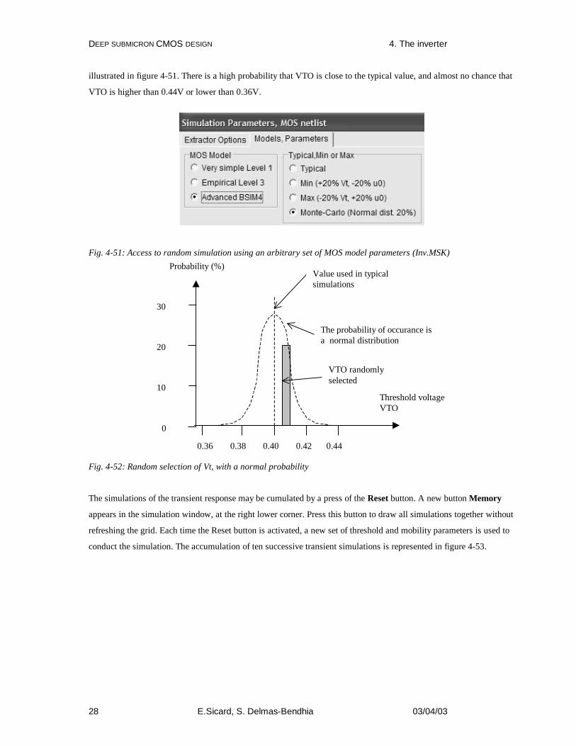
7. Random simulation
As explained in chapter 3, unavoidable process variations may occur during the integrated circuit fabrication, which
may impact the static and dynamic characteristics of the inverter. In the menu Simulate ? Simulation parameters
the default set of parameters corresponds to the "typical" case. We may simulate the inverter in "minimum" or
"maximum" case, as we did for the MOS device. An interesting alternative consists in using the "random" mode, also
called "Monte-Carlo" analysis, where the threshold voltage and the mobility are chosen in a random way, as
DEEP SUBMICRON CMOS DESIGN 4. The inverter
28 E.Sicard, S. Delmas-Bendhia 03/04/03
illustrated in figure 4-51. There is a high probability that VTO is close to the typical value, and almost no chance that
VTO is higher than 0.44V or lower than 0.36V.
Fig. 4-51: Access to random simulation using an arbitrary set of MOS model parameters (Inv.MSK)
Threshold voltage VTO
0.40 0.42 0.36 0.38 0.44
The probability of occurance is a normal distribution
Probability (%)
0
10
20
30
Value used in typical simulations
VTO randomly selected
Fig. 4-52: Random selection of Vt, with a normal probability
The simulations of the transient response may be cumulated by a press of the Reset button. A new button Memory
appears in the simulation window, at the right lower corner. Press this button to draw all simulations together without
refreshing the grid. Each time the Reset button is activated, a new set of threshold and mobility parameters is used to
conduct the simulation. The accumulation of ten successive transient simulations is represented in figure 4-53.

DEEP SUBMICRON CMOS DESIGN 4. The inverter
29 E.Sicard, S. Delmas-Bendhia 03/04/03
The rise delay fluctuates
The fall delay fluctuates
10 successive simulations (Memory on)
Fig. 4-53: The Monte-Carlo simulation of the inverter transient characteristics, using random VTO and UO
parameters (Inv.MSK).
The inverter has a strong probability behave close to the typical value. In some rare case, the switching performances
vary significantly. The min/max simulation is also very interesting to simulate the inverter in extreme situations.
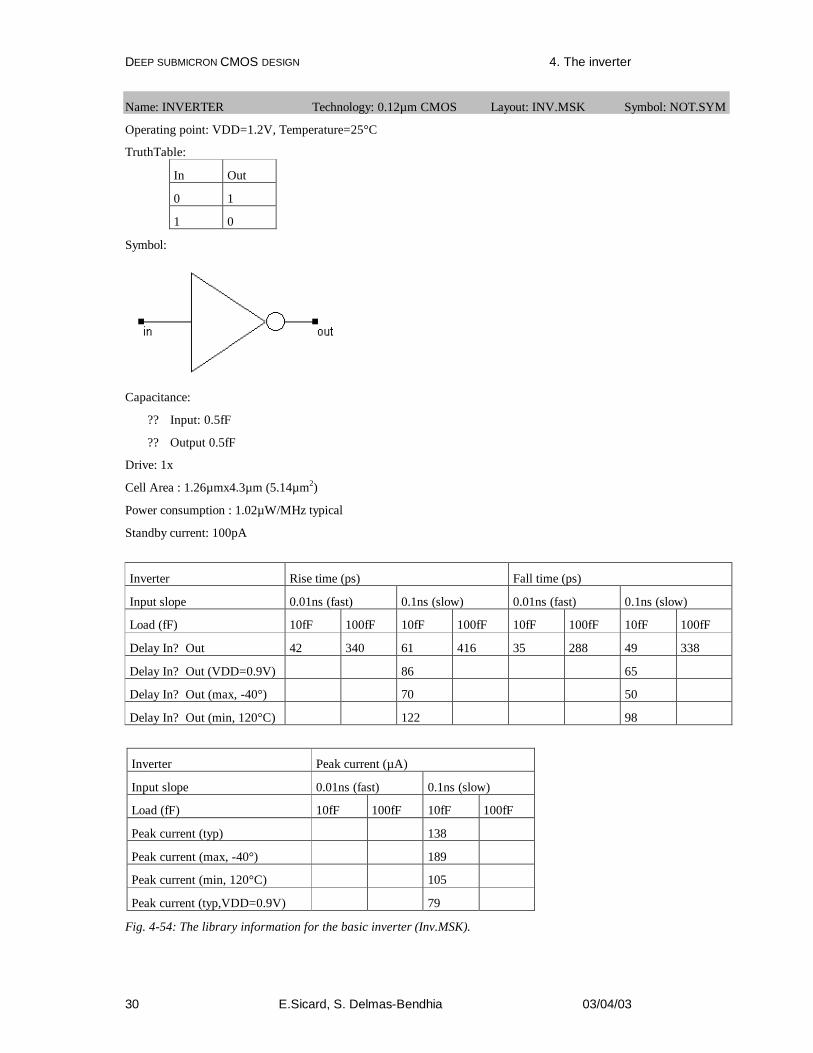
8. The Inverter as a library cell
Generally speaking, the integrated circuit design relies on a library of basic cells. In this library, each basic cell is
described in a very detailed way. The layout information and several static and dynamic aspects are usually included.
Such details are important for choosing the appropriate cell, to evaluate the circuit size, standby parasitic current and
switching performances.
The data-sheet of the inverter usually looks like figure 4-54. Firstly, the header gives the cell name. The mask level
file and symbol files are also listed. The truth table recalls the logic behavior of the cell. The symbol is also provided.
In the case of complex cells such as latches, where numerous versions and options co-exist beyond the same name, the
truth-table is of key importance. The node capacitance is useful for propagation delay prediction, as the switching
performance are linked with the capacitance load.
The operating point recalls the value of the supply with which the characterization has been conducted. Some
information are also given for low supply voltage (See also the switching characteristics at 0.9V).
DEEP SUBMICRON CMOS DESIGN 4. The inverter
30 E.Sicard, S. Delmas-Bendhia 03/04/03
Name: INVERTER Technology: 0.12µm CMOS Layout: INV.MSK Symbol: NOT.SYM
Operating point: VDD=1.2V, Temperature=25°C
TruthTable:
In Out
0 1
1 0
Symbol:
Capacitance:
? ? Input: 0.5fF
? ? Output 0.5fF
Drive: 1x
Cell Area : 1.26µmx4.3µm (5.14µm2)
Power consumption : 1.02µW/MHz typical
Standby current: 100pA
Inverter Rise time (ps) Fall time (ps)
Input slope 0.01ns (fast) 0.1ns (slow) 0.01ns (fast) 0.1ns (slow)
Load (fF) 10fF 100fF 10fF 100fF 10fF 100fF 10fF 100fF
Delay In? Out 42 340 61 416 35 288 49 338
Delay In? Out (VDD=0.9V) 86 65
Delay In? Out (max, -40°) 70 50
Delay In? Out (min, 120°C) 122 98
Inverter Peak current (µA)
Input slope 0.01ns (fast) 0.1ns (slow)
Load (fF) 10fF 100fF 10fF 100fF
Peak current (typ) 138
Peak current (max, -40°) 189
Peak current (min, 120°C) 105
Peak current (typ,VDD=0.9V) 79
Fig. 4-54: The library information for the basic inverter (Inv.MSK).

DEEP SUBMICRON CMOS DESIGN 4. The inverter
31 E.Sicard, S. Delmas-Bendhia 03/04/03
The power consumption is usually described in µW/MHz. To characterize this value, a 1MHz clock is connected to
the input and the total power consumption is computed from the integral of the current. In Microwind, we preferably
use a 1GHz clock, and consequently divide the power estimation by 1000. The cell consumption increase linearly with
frequency. The standby current is a key information in low-power circuits, where the standby parasitic current should
be as small as possible. Depending on the MOS option (normal, high-speed, low leakage), the standby current may
vary in a very significant way.
The keyword "1x" refers to the inverter strength. A cell with 1x strength has small output MOS devices, usually close
from the minimum length and width. A cell with 2x has medium size MOS devices, a cell with drive 4x is used for
high speed signals. Cells with 8x drive or even 16x drive may exist, to propagate very fast signals such as clocks and
bus. However, using cells with high drive means a high power consumption and high risks of signal integrity
problems.
The delay between signals in and out is strongly dependant on the slope of the input signal, the capacitance connected
to the output signal, the temperature, the power supply and the process variations. The goal of the switching delay
table is to summarize the delay in typical conditions as well as extreme conditions. Several design tools such as the
timing analyzer and the power consumption extractor will use these data to guess all possible cases of loading
conditions, temperature variation, etc.
Small load (10fF)
Capacitance
Large load (100fF)
Delay 1
Delay 2
DelayValues in
library
Interpolation performedby timing analysis tools
Typical
Minimum
Maximum
Fig. 4-55: Delay parameters are used by timing analysis tools to predict the cell switching performances for any
capacitance
The current peak details are used to evaluate the power consumption of the circuit. The value of the current changes
significantly depending on the loading conditions, temperature and supply voltage, as expected.
9. 3-State Inverter

DEEP SUBMICRON CMOS DESIGN 4. The inverter
32 E.Sicard, S. Delmas-Bendhia 03/04/03
Until now all the symbols produced the value logic ‘0’ and logic ‘1’. However, if several inverters share the same
node, such as a bus structures (Figure 4-56), conflicts will rise. In order to avoid multiple access at the same time,
specific circuits called 3-state inverters are used, featuring the possibility to remain in a ‘high impedance’ state when
access is not required.
Figure 4-56: If multiple access is required on a single node, 3-state inverters are used for interfacing (Inv3state.SCH)
The 3-state inverter symbol consists of the logic inverter and an enable control circuit. The output remains in ‘high
impedance’ (Logic symbol 'X') as long as the enable En is set to level ‘0’. The truth table is reported below.
NOTIF1
In En Out
0 0 X
0 1 1
1 0 X
1 1 0
x 0 or 1 X
0 or 1 X X
The internal structure of the 3-state inverter is shown in figure 4-57. The basic CMOS inverter is no more connected
to the supply lines VDD and VSS directly. In contrary, pass nMOS and pMOS devices are inserted to disconnect the
inverter when the cell is disabled.

DEEP SUBMICRON CMOS DESIGN 4. The inverter
33 E.Sicard, S. Delmas-Bendhia 03/04/03
Figure 4-57: Schematic diagram and logic symbol for the 3-state inverter (CmosInv3State.SCH)
Unfortunately, a supplementary inverter is needed to generate the /enable signal required to control the pMOS device.
The logic simulation reported in figure 4-58 illustrates two basic situations: one where enable is inactive, and the
output is in high-impedance state <glossary> as no path exists to VDD or VSS, the other where the circuit is
equivalent to an inverter, as the upper and lower pass transistors are enabled.
Figure 4-58: Simulation of the 3-state inverter (CmosInv3State.SCH)
Two versions of layout are proposed in figure 4-59, which correspond to the same design. The cell situated on the left
is the direct implementation of the schematic diagram of the 3-state inverter. The layout implementation is not
optimal as we loose some silicon area due to severe diffusion design rules which require a 4 lambda spacing. The new
arrangement, shown in the right of the figure, is significantly more compact, thanks to an horizontal flip of the
Enable inverter, and the sharing of the ground and supply contacts, as illustrated in figure 4-60. Continuous
diffusions always lead to more compact and faster designs.

DEEP SUBMICRON CMOS DESIGN 4. The inverter
34 E.Sicard, S. Delmas-Bendhia 03/04/03
Figure 4-59: The layout of the 3-state inverter (Inv3State.MSK)
5?
4?
6?
A A
B C
A
B C
Figure 4-60: A permutation technique to achieve more compact layout
The analog simulation reported in figure 4-61 gives an interesting view of the high impedance state. From the
chronograms, we see that when Enable=1 the cell acts as a regular CMOS inverter, while when Enable=0 the output
"floats" in an unpredictable voltage value, which tends to fluctuate at the switching of the input, mainly due to
parasitic leakage and couplings.

DEEP SUBMICRON CMOS DESIGN 4. The inverter
35 E.Sicard, S. Delmas-Bendhia 03/04/03
Figure 4-61: Analog simulation of the 3-state inverter (INV3STATE.MSK)
10. All nMOS Inverters Several other circuits exist to realize the logic inverter function [Baker page 224]. One popular inverter is shown in
figure 4-62. It consists of a normal n-channel MOS device and a strange n-channel MOS device connected as a simple
load. In that case, the nMOS device is used as a resistance. The simulation waveforms are quite unusual as the low
state (In=1) of the output leads to stand-by current which did not appear until now in CMOS circuits. This DC power
waste is a major drawback for this kind of design. Furthermore, the logic level 0 corresponds to 0.3V while the logic
level 1 corresponds to 0.8V. The switching is slow, specifically from 0 to 1, due to a weak nMOS device. However, no
pMOS device is required, which simplifies both the design and the process. All n-MOS inverters were used before
CMOS technology was made available.

DEEP SUBMICRON CMOS DESIGN 4. The inverter
36 E.Sicard, S. Delmas-Bendhia 03/04/03
Figure 4-62: All n-MOS inverter(INVNMOS.MSK)
11. Ring Oscillator
The ring oscillator made from 5 inverters has the property to oscillate naturally. We observe the oscillating output and
measure its corresponding frequency.

DEEP SUBMICRON CMOS DESIGN 4. The inverter
37 E.Sicard, S. Delmas-Bendhia 03/04/03
Figure 4-63: Schematic diagram and layout of the ring oscillator used for simulation (INV5.MSK)
The ring oscillator circuit can be simulated easily at layout level with MICROWIND2 using various technologies. The
time-domain waveform of the output are reported in figure 4-64 for 0.8, 0.12µm and 70nm technologies. Although the
supply voltage (VDD) has been reduced (VDD is 5V in 0.8µm, 1.2V in 0.12µm, and 0.7V in 70nm), the gain in
frequency improvement is significant.
Technology Supply Oscillation Chronograms 0.8 µm 5V 0.76GHz
0.12 µm 1.2V 32GHz
90nm 1.0V 41GHz
Fig. 4-64: Oscillation frequency improvement with the technology scale down (Inv5.MSK)

DEEP SUBMICRON CMOS DESIGN 4. The inverter
38 E.Sicard, S. Delmas-Bendhia 03/04/03
By default the software is configured with 0.12µm technology. Use the command File ? Select Foundry to change
the configuring technology. For example, select cmos08.RUL which corresponds to the CMOS 0.8µm technology, or
the file cmos90nm.RUL which configures Microwind to the CMOS 90nm technology. When you run again the
simulation, you may observe the change of VDD and the significant change in oscillating frequency.
High Speed vs. Low leakage
Let us consider the ring oscillator with an enable circuit, where one inverter has been replaced by a NAND gate to
enable or disable oscillation (Inv5Enable.MSK). The schematic diagram is shown in figure 4-65, as well as its
layout implementation. We analyze the switching performances in high speed and low leakage mode, by changing
the properties of the option layer which surrounds all devices.
Fig. 4-65 The schematic diagram and layout of the ring oscillator used to compare the analog performances in high
speed and low leakage mode (INV5Enable.MSK)

DEEP SUBMICRON CMOS DESIGN 4. The inverter
39 E.Sicard, S. Delmas-Bendhia 03/04/03
Fast oscillation (26GHz)
Strong consumption (1mA max)
High standby current
Fig. 4-66: Simulation of the ring oscillator in high speed mode, using BSIM4 model. The oscillating frequency is fast
but the standby current is high (Inv5Enable.MSK)
Reduced peak current (0.57mA)
Very low standby current
20GHz oscillation
Fig. 4-67: Simulation of the ring oscillator in low voltage mode, using BSIM4 model. The oscillating frequency is
slower but the standby current is very low (Inv5Enable.MSK)

DEEP SUBMICRON CMOS DESIGN 4. The inverter
40 E.Sicard, S. Delmas-Bendhia 03/04/03
Parameter Low leakage mode High Speed mode Imax 0.6 mA 1.0mA I standby <1nA >10nA Oscillating frequency 20GHz 26GHz
Table 4-4: Comparative performances of the ring oscillator (Inv5Enable.MSK)
The option layer which surrounds the oscillator is set to high speed mode by a double click inside that box. In high
speed mode, the circuit works fast (26GHz) but consumes a lot of power (1mA) when on, and a significant standby
current when off (10nA), as shown in the simulation of the voltage and current given figure 4-66. Notice the tick in
front of "Scale I in log" to display the current in logarithmic scale.
In contrast, the low leakage MOS features slower oscillation ( 20GHz in figure 4-67, that is approximately a 25%
speed reduction) , but with 40% less current when ON, and more than one decade less standby current when off
(1nA). In summary, low leakage MOS devices should be used whenever possible. High speed MOS should be used
only when speed is critical, such as communication bus, critical path, etc.. The analog performances are summarized
in table 4-4.
Temperature effects
The main consequence of temperature increase is the decrease of mobility of electrons and holes of the MOS channel,
leading to slower transient performances. Thus, the propagation delay due to the logic gate is increased, as illustrated
in figure 4-68 which concerns the switching characteristics of the 5-inverter ring oscillator. In Microwind2, you can
get access to temperature using the command Simulate ? Simulation Parameters. The temperature is given in °C.
T=27°C
T=120°C
Fig. 4-68. Propagation delay increase with temperature (Inv5Enable.MSK)

DEEP SUBMICRON CMOS DESIGN 4. The inverter
41 E.Sicard, S. Delmas-Bendhia 03/04/03
In the simulation of figure 4-68, we used the BSIM4 model for a temperature set to 25°C and 120°C. We can observe
a 10% decrease of switching speed, which finds its origin in the mobility degradation, which is computed by the
following formulation.
8.1)27( )
300273(00 ?
??? TUU T (eq. 4-4)
We may conduct the parametric analysis of the temperature influence on the oscillating frequency, in order to obtain
the results reported in figure 4-69. It may be seen that the frequency variation from -100°C to +100°C is kept below
15%. The reason of this reduced dependence is that the mobility reduction is compensated by the threshold voltage
decrease, also strongly dependent on the temperature, which tends to limit the overall effects of temperature
variations.
Fig. 4-69: Performances of the ring oscillator versus temperature increase (Inv5Enable.MSK)
A 2.5GHz ring oscillator
The previous ring oscillator operates around 30GHz, which is of no practical use. In contrast, the 2.5GHz frequency is
widely used for a variety of wireless network applications. In this paragraph, we investigate several possibilities for
slowing the oscillator frequency down to 2.5GHz. One immediate idea consists in designing a ring oscillator with
more inverter stages (Around 70). This is a power consuming and silicon area consuming approach. A more attractive
solution consists in the reduction of the MOS current capabilities. Then a new question rises: how should we proceed,

DEEP SUBMICRON CMOS DESIGN 4. The inverter
42 E.Sicard, S. Delmas-Bendhia 03/04/03
as we may increase the channel length, decrease the channel width, or add parasitic capacitance in each switching
node (Figure 4-70)?
Increase the length
Decrease the width
Add parasitic capacitance
Figure 4-70: Reducing the current of the MOS device may be performed by increasing the length or decreasing the
width
One solution is proposed in figure 4-71. It combines the channel length increase, the width decrease to its minimum
value, and the enlarging of drain areas whenever possible to increase the parasitic junction surface, and consequently
its parasitic capacitance. All these layout modification have a sufficient impact to reduce the oscillating frequency to
around 2.5GHz. Notice that this frequency is very sensitive to process parameters, temperature, and supply voltage
variation.
Figure 4-70: The 5-inverter oscillator tuned to 2.5GHz (Inv2,5GHz.MSK)
12. Latch-up effect
The latch-up effect is a parasitic shortcut between VDD and VSS that can lead to the destruction of the integrated
circuits. The origin of latch-up is the activation of a parasitic N/P/N/P device (Also called thyristor) appearing in the
vertical cross-section of the nMOS and pMOS structures as reported in figure 4-71.

DEEP SUBMICRON CMOS DESIGN 4. The inverter
43 E.Sicard, S. Delmas-Bendhia 03/04/03
VDDVSS
Possible parasitic path dueto latch-up
Fig. 4-71. Origin of latch-up
Limiting the latch-up effect
The latch-up effect is almost eliminated if the substrate is locally polarized to ground, and the n-well is locally
polarized to VDD (Figure 4-72). In the upper layout (Figure 4-72a), the situation is extremely dangerous as the n-well
region is floating. If the n-well potential drops around VDD/2 and the local substrate voltage rises to VDD/2, the
latch-up phenomenon is initiated. Most layout tools alert the designer in the case of floating n-well regions. The good
approach consists in inserting a polarization diode N+/N-well and stuck it to the highest possible potential, typically
VDD.

DEEP SUBMICRON CMOS DESIGN 4. The inverter
44 E.Sicard, S. Delmas-Bendhia 03/04/03
Floating n-well
N+ contact to n-well, connected to VDD
Very probable path from VDD to VSS
N+ contact to n-well, connected to VDD
P+ contact to p-substrate connected to VSS
The p-substrate voltage could rise as no polarization exist locally
Possible path from VDD to VSS
(a)
(b)
(c)
Fig. 4-72. Limiting the latch-up effect by polarization diodes
Many designers consider that there exists an « automatic » polarization of the substrate to ground and forget to add a
local P+/P-substrate contact to ground, near the nMOS device (Figure 4-72b). This might be a dangerous assumption
which can cause latch-up: in 0.12µm technologies, several manufacturers use highly resistive p-doped substrate. In
that case, the electrical link between the physical ground (Back of the IC) and the local nMOS area is equivalent to a
resistor of several Kohm. Consequently, what is supposed to be a good 0V reference is a very weak 0V, that can easily
fluctuate and turn on the N/P/N/P device, which may lead to latch-up and possible destruction. This is why it is highly
recommended to add also a P+/P-substrate polarization to ground, which protects the logic cell from latch-up (Figure
4-72c).
13. CONCLUSION
This chapter has described the CMOS inverter, from a logic and analog point of view. The mobility difference
between electrons and holes has been counterbalanced at layout level to obtain symmetrical static and dynamic
characteristics. The effect of MOS model and temperature on the simulation results have also been investigated. The

DEEP SUBMICRON CMOS DESIGN 4. The inverter
45 E.Sicard, S. Delmas-Bendhia 03/04/03
3-state inverter, all n-MOS inverter and ring-oscillator circuits has been designed and simulated. Finally, we
presented the basic polarization techniques to avoid the parasitic latchup effect.
REFERENCES [Weste] N. Weste, K. Eshraghian "Principles of CMOS VLSI design", Addison Wesley, ISBN 0-201-53376-6, 1993
[Baker] R.J. Baker, H. W. Li, D.E. Boyce "CMOS circuit design, layout and simulation", IEEE Press, ISBN 0-7803-
3416-7, 1998
EXERCISES 1. <Complete the INV form>
2. We consider 3 inverters, Inv1 with Wp=Wn, Inv2 with Wp>Wn, Inv3 with Wp<Wn. From the static characteristics
shown in figure 4-xxx, assign the curves to the corresponding inverters.
1
2
3
Vin
Vout
Fig. 4-xxx. Inverter characteristics
<Sonia's other exo>
3. Investigate sensitive to process parameters,
4. Investigate sensitive to temperature.